JP4921913B2 - 基板洗浄方法 - Google Patents
基板洗浄方法 Download PDFInfo
- Publication number
- JP4921913B2 JP4921913B2 JP2006271072A JP2006271072A JP4921913B2 JP 4921913 B2 JP4921913 B2 JP 4921913B2 JP 2006271072 A JP2006271072 A JP 2006271072A JP 2006271072 A JP2006271072 A JP 2006271072A JP 4921913 B2 JP4921913 B2 JP 4921913B2
- Authority
- JP
- Japan
- Prior art keywords
- substrate
- cleaning
- nozzle
- cleaning liquid
- water
- Prior art date
- Legal status (The legal status is an assumption and is not a legal conclusion. Google has not performed a legal analysis and makes no representation as to the accuracy of the status listed.)
- Expired - Fee Related
Links
Images


Classifications
-
- B—PERFORMING OPERATIONS; TRANSPORTING
- B08—CLEANING
- B08B—CLEANING IN GENERAL; PREVENTION OF FOULING IN GENERAL
- B08B3/00—Cleaning by methods involving the use or presence of liquid or steam
- B08B3/02—Cleaning by the force of jets or sprays
- B08B3/024—Cleaning by means of spray elements moving over the surface to be cleaned
-
- H—ELECTRICITY
- H10—SEMICONDUCTOR DEVICES; ELECTRIC SOLID-STATE DEVICES NOT OTHERWISE PROVIDED FOR
- H10P—GENERIC PROCESSES OR APPARATUS FOR THE MANUFACTURE OR TREATMENT OF DEVICES COVERED BY CLASS H10
- H10P72/00—Handling or holding of wafers, substrates or devices during manufacture or treatment thereof
- H10P72/04—Apparatus for manufacture or treatment
- H10P72/0402—Apparatus for fluid treatment
- H10P72/0406—Apparatus for fluid treatment for cleaning followed by drying, rinsing, stripping, blasting or the like
- H10P72/0411—Apparatus for fluid treatment for cleaning followed by drying, rinsing, stripping, blasting or the like for wet cleaning or washing
- H10P72/0414—Apparatus for fluid treatment for cleaning followed by drying, rinsing, stripping, blasting or the like for wet cleaning or washing using mainly spraying means, e.g. nozzles
Landscapes
- Cleaning Or Drying Semiconductors (AREA)
- Exposure Of Semiconductors, Excluding Electron Or Ion Beam Exposure (AREA)
Description
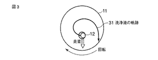
図1は、第1の実施の形態の基板洗浄方法を示す図である。なお、本基板洗浄方法は、基板洗浄装置内の図示しない制御装置の制御により行われる。図1に示すように、半導体ウエハなどの被処理基板11を洗浄する工程において、被処理基板11上方のノズル12から洗浄液13を吐出し、基板11を回転させながら基板11を洗浄、乾燥する。
第2の実施の形態においては、第1の実施の形態と同様の基板に対して同様の材料を積層塗布形成し、ArF液浸露光装置にて液浸露光を行った。
第1の実施の形態においては、基板を液浸露光後に洗浄工程を行ったが、本第3の実施の形態においては液浸露光前にも洗浄工程を行う方法を説明する。
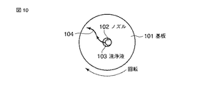
第4の実施の形態は第1の実施の形態と同様の構成であるが、ノズルのスキャン速度Vsがノズルの位置の基板の角速度ωnzと比例関係(Vs∝ωnz)で表されるよう、ノズルを基板の外周に向かって加速しながら洗浄していく方法である。
Claims (5)
- 被処理基板の上方のノズルから洗浄液を吐出し、前記基板を回転させながら前記基板を洗浄する基板洗浄方法であり、前記ノズルから前記洗浄液を前記基板に吐出しながら、前記ノズルを前記基板の中心から前記基板の外側へ走査し、前記洗浄液を前記基板の外側に散逸させる基板洗浄方法において、
前記基板上に滞留している洗浄液が存在する状態で、前記ノズルから吐出された前記洗浄液が前記基板表面に接触した際、前記ノズルから吐出された前記洗浄液が、前記基板上に滞留している前記洗浄液に衝突しないように、前記洗浄液の流量、前記基板の回転数、前記ノズルの走査速度と走査開始位置を制御することを特徴とする基板洗浄方法。 - 前記ノズルの走査速度は、前記ノズルから吐出した前記洗浄液が前記基板上で跳水現象を起こしている領域の半径と前記基板の単位時間あたりの回転数との積と比例関係を持つことを特徴とする請求項1に記載の基板洗浄方法。
- 前記ノズルの走査開始位置は、前記ノズルから吐出した前記洗浄液が前記基板上で跳水現象を起こしている領域の半径と比例の関係で表された位置とすることを特徴とする請求項1に記載の基板洗浄方法。
- 前記洗浄液の流量は、前記ノズルから吐出した前記洗浄液が前記基板上で跳水現象を起こしている領域の半径により決まることを特徴とする請求項1に記載の基板洗浄方法。
- 他のノズルから洗浄液を前記基板の裏面に吐出することを特徴とする請求項1に記載の基板洗浄方法。
Priority Applications (2)
| Application Number | Priority Date | Filing Date | Title |
|---|---|---|---|
| JP2006271072A JP4921913B2 (ja) | 2006-10-02 | 2006-10-02 | 基板洗浄方法 |
| US11/865,901 US20080078427A1 (en) | 2006-10-02 | 2007-10-02 | Substrate cleaning method and semiconductor device manufacturing method |
Applications Claiming Priority (1)
| Application Number | Priority Date | Filing Date | Title |
|---|---|---|---|
| JP2006271072A JP4921913B2 (ja) | 2006-10-02 | 2006-10-02 | 基板洗浄方法 |
Publications (3)
| Publication Number | Publication Date |
|---|---|
| JP2008091637A JP2008091637A (ja) | 2008-04-17 |
| JP2008091637A5 JP2008091637A5 (ja) | 2009-10-08 |
| JP4921913B2 true JP4921913B2 (ja) | 2012-04-25 |
Family
ID=39259935
Family Applications (1)
| Application Number | Title | Priority Date | Filing Date |
|---|---|---|---|
| JP2006271072A Expired - Fee Related JP4921913B2 (ja) | 2006-10-02 | 2006-10-02 | 基板洗浄方法 |
Country Status (2)
| Country | Link |
|---|---|
| US (1) | US20080078427A1 (ja) |
| JP (1) | JP4921913B2 (ja) |
Families Citing this family (9)
| Publication number | Priority date | Publication date | Assignee | Title |
|---|---|---|---|---|
| JP4926678B2 (ja) * | 2006-12-04 | 2012-05-09 | 東京エレクトロン株式会社 | 液浸露光用洗浄装置および洗浄方法、ならびにコンピュータプログラムおよび記憶媒体 |
| JP2009111186A (ja) * | 2007-10-30 | 2009-05-21 | Toshiba Corp | 基板処理方法、基板搬送方法および基板搬送装置 |
| JP5159738B2 (ja) * | 2009-09-24 | 2013-03-13 | 株式会社東芝 | 半導体基板の洗浄方法および半導体基板の洗浄装置 |
| US9698062B2 (en) * | 2013-02-28 | 2017-07-04 | Veeco Precision Surface Processing Llc | System and method for performing a wet etching process |
| JP2017536692A (ja) | 2014-10-31 | 2017-12-07 | ビーコ プリジション サーフェイス プロセシング エルエルシー | ウェット・エッチング・プロセスを実行するための装置および方法 |
| US9870928B2 (en) | 2014-10-31 | 2018-01-16 | Veeco Precision Surface Processing Llc | System and method for updating an arm scan profile through a graphical user interface |
| TWI738757B (zh) | 2016-04-05 | 2021-09-11 | 美商維克儀器公司 | 經由化學的適應性峰化來控制蝕刻速率的裝置和方法 |
| CN106057710B (zh) * | 2016-08-02 | 2019-02-19 | 北京七星华创电子股份有限公司 | 改善气液两相雾化清洗均匀性的装置和方法 |
| EP3590128A1 (en) | 2017-03-03 | 2020-01-08 | Veeco Precision Surface Processing LLC | An apparatus and method for wafer thinning in advanced packaging applications |
Family Cites Families (8)
| Publication number | Priority date | Publication date | Assignee | Title |
|---|---|---|---|---|
| JP2002239434A (ja) * | 2001-02-14 | 2002-08-27 | Tokyo Electron Ltd | 塗布膜形成装置および塗布膜形成方法 |
| JP3655576B2 (ja) * | 2001-07-26 | 2005-06-02 | 株式会社東芝 | 液膜形成方法及び半導体装置の製造方法 |
| US20030192570A1 (en) * | 2002-04-11 | 2003-10-16 | Applied Materials, Inc. | Method and apparatus for wafer cleaning |
| JP2004335542A (ja) * | 2003-04-30 | 2004-11-25 | Toshiba Corp | 基板洗浄方法及び基板乾燥方法 |
| JP2006024715A (ja) * | 2004-07-07 | 2006-01-26 | Toshiba Corp | リソグラフィー装置およびパターン形成方法 |
| JP4324527B2 (ja) * | 2004-09-09 | 2009-09-02 | 東京エレクトロン株式会社 | 基板洗浄方法及び現像装置 |
| JP4459774B2 (ja) * | 2004-10-12 | 2010-04-28 | 東京エレクトロン株式会社 | 基板処理方法、基板処理装置およびコンピュータプログラム |
| US7476616B2 (en) * | 2004-12-13 | 2009-01-13 | Fsi International, Inc. | Reagent activator for electroless plating |
-
2006
- 2006-10-02 JP JP2006271072A patent/JP4921913B2/ja not_active Expired - Fee Related
-
2007
- 2007-10-02 US US11/865,901 patent/US20080078427A1/en not_active Abandoned
Also Published As
| Publication number | Publication date |
|---|---|
| JP2008091637A (ja) | 2008-04-17 |
| US20080078427A1 (en) | 2008-04-03 |
Similar Documents
| Publication | Publication Date | Title |
|---|---|---|
| US20220277968A1 (en) | Substrate cleaning method, substrate cleaning system, and memory medium | |
| US6864187B2 (en) | Method of washing a semiconductor wafer | |
| TWI619190B (zh) | Liquid processing method, memory medium and liquid processing device | |
| US20080078427A1 (en) | Substrate cleaning method and semiconductor device manufacturing method | |
| US7926439B2 (en) | Substrate processing apparatus | |
| JP5680705B2 (ja) | 基板処理方法 | |
| JP2007019161A (ja) | パターン形成方法及び被膜形成装置 | |
| JP2021073739A (ja) | 基板洗浄方法 | |
| JP5276559B2 (ja) | 基板処理方法および基板処理装置 | |
| JP7470785B2 (ja) | 洗浄装置および洗浄方法 | |
| US6090534A (en) | Device and method of decreasing circular defects and charge buildup integrated circuit fabrication | |
| JP4919409B2 (ja) | 半導体装置製造方法 | |
| US9937520B2 (en) | Substrate treating method | |
| JP2008249854A (ja) | フォトマスクの洗浄方法 | |
| JP2006245381A (ja) | 基板洗浄乾燥装置および方法 | |
| US20180226268A1 (en) | Semiconductor manufacturing apparatus and manufacturing method of semiconductor device | |
| CN113823550B (zh) | 一种晶圆边缘上的可旋涂硬掩模去除方法 | |
| JP2008258441A (ja) | 基板処理方法及び基板処理装置 | |
| JP2008016781A (ja) | 基板処理方法および基板処理装置 | |
| JP2008171923A (ja) | ウェハ洗浄装置、ウェハ洗浄方法 | |
| JP4492931B2 (ja) | フォトレジストパターンの形成方法 | |
| KR20060065616A (ko) | 기판 세정 건조 방법 | |
| KR100641540B1 (ko) | 레지스트 코팅 장비 및 이를 세정하는 방법 | |
| KR100744277B1 (ko) | 웨이퍼의 에지 비드 제거장치 | |
| KR102596300B1 (ko) | 기판 세정 장치 |
Legal Events
| Date | Code | Title | Description |
|---|---|---|---|
| A521 | Request for written amendment filed |
Free format text: JAPANESE INTERMEDIATE CODE: A523 Effective date: 20090825 |
|
| A621 | Written request for application examination |
Free format text: JAPANESE INTERMEDIATE CODE: A621 Effective date: 20090825 |
|
| A977 | Report on retrieval |
Free format text: JAPANESE INTERMEDIATE CODE: A971007 Effective date: 20110307 |
|
| A131 | Notification of reasons for refusal |
Free format text: JAPANESE INTERMEDIATE CODE: A131 Effective date: 20110412 |
|
| A521 | Request for written amendment filed |
Free format text: JAPANESE INTERMEDIATE CODE: A523 Effective date: 20110613 |
|
| TRDD | Decision of grant or rejection written | ||
| A01 | Written decision to grant a patent or to grant a registration (utility model) |
Free format text: JAPANESE INTERMEDIATE CODE: A01 Effective date: 20120110 |
|
| A01 | Written decision to grant a patent or to grant a registration (utility model) |
Free format text: JAPANESE INTERMEDIATE CODE: A01 |
|
| A61 | First payment of annual fees (during grant procedure) |
Free format text: JAPANESE INTERMEDIATE CODE: A61 Effective date: 20120203 |
|
| FPAY | Renewal fee payment (event date is renewal date of database) |
Free format text: PAYMENT UNTIL: 20150210 Year of fee payment: 3 |
|
| LAPS | Cancellation because of no payment of annual fees |