JP4876987B2 - 受信回路 - Google Patents
受信回路 Download PDFInfo
- Publication number
- JP4876987B2 JP4876987B2 JP2007062404A JP2007062404A JP4876987B2 JP 4876987 B2 JP4876987 B2 JP 4876987B2 JP 2007062404 A JP2007062404 A JP 2007062404A JP 2007062404 A JP2007062404 A JP 2007062404A JP 4876987 B2 JP4876987 B2 JP 4876987B2
- Authority
- JP
- Japan
- Prior art keywords
- terminal
- potential line
- transistor
- resistor
- resistance
- Prior art date
- Legal status (The legal status is an assumption and is not a legal conclusion. Google has not performed a legal analysis and makes no representation as to the accuracy of the status listed.)
- Active
Links
Images


Classifications
-
- H—ELECTRICITY
- H03—ELECTRONIC CIRCUITRY
- H03F—AMPLIFIERS
- H03F3/00—Amplifiers with only discharge tubes or only semiconductor devices as amplifying elements
- H03F3/04—Amplifiers with only discharge tubes or only semiconductor devices as amplifying elements with semiconductor devices only
- H03F3/08—Amplifiers with only discharge tubes or only semiconductor devices as amplifying elements with semiconductor devices only controlled by light
- H03F3/082—Amplifiers with only discharge tubes or only semiconductor devices as amplifying elements with semiconductor devices only controlled by light with FET's
-
- H—ELECTRICITY
- H03—ELECTRONIC CIRCUITRY
- H03F—AMPLIFIERS
- H03F3/00—Amplifiers with only discharge tubes or only semiconductor devices as amplifying elements
- H03F3/45—Differential amplifiers
- H03F3/45071—Differential amplifiers with semiconductor devices only
- H03F3/45076—Differential amplifiers with semiconductor devices only characterised by the way of implementation of the active amplifying circuit in the differential amplifier
- H03F3/45475—Differential amplifiers with semiconductor devices only characterised by the way of implementation of the active amplifying circuit in the differential amplifier using IC blocks as the active amplifying circuit
-
- H—ELECTRICITY
- H03—ELECTRONIC CIRCUITRY
- H03F—AMPLIFIERS
- H03F2203/00—Indexing scheme relating to amplifiers with only discharge tubes or only semiconductor devices as amplifying elements covered by H03F3/00
- H03F2203/45—Indexing scheme relating to differential amplifiers
- H03F2203/45008—Indexing scheme relating to differential amplifiers the addition of two signals being made by a resistor addition circuit for producing the common mode signal
-
- H—ELECTRICITY
- H03—ELECTRONIC CIRCUITRY
- H03F—AMPLIFIERS
- H03F2203/00—Indexing scheme relating to amplifiers with only discharge tubes or only semiconductor devices as amplifying elements covered by H03F3/00
- H03F2203/45—Indexing scheme relating to differential amplifiers
- H03F2203/45138—Two or more differential amplifiers in IC-block form are combined, e.g. measuring amplifiers
-
- H—ELECTRICITY
- H03—ELECTRONIC CIRCUITRY
- H03F—AMPLIFIERS
- H03F2203/00—Indexing scheme relating to amplifiers with only discharge tubes or only semiconductor devices as amplifying elements covered by H03F3/00
- H03F2203/45—Indexing scheme relating to differential amplifiers
- H03F2203/45561—Indexing scheme relating to differential amplifiers the IC being controlled, e.g. by a signal derived from a non specified place in the dif amp circuit
-
- H—ELECTRICITY
- H03—ELECTRONIC CIRCUITRY
- H03F—AMPLIFIERS
- H03F2203/00—Indexing scheme relating to amplifiers with only discharge tubes or only semiconductor devices as amplifying elements covered by H03F3/00
- H03F2203/45—Indexing scheme relating to differential amplifiers
- H03F2203/45576—Indexing scheme relating to differential amplifiers the IC comprising input impedance adapting or controlling means
Landscapes
- Engineering & Computer Science (AREA)
- Power Engineering (AREA)
- Logic Circuits (AREA)
- Dc Digital Transmission (AREA)
- Cable Transmission Systems, Equalization Of Radio And Reduction Of Echo (AREA)
- Amplifiers (AREA)
Description
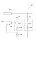
図1は、本発明に係る受信回路の第1実施形態の構成を示す回路図である。同図に示す受信回路1aは、差動信号SDを受信する回路であって、差動信号SDのうち正相信号SPを外部から受信する第1の端子2と、差動信号SDのうち逆相信号SNを外部から受信する第2の端子3と、正相信号SP及び逆相信号SNを増幅して受信信号Sinを生成する増幅器4と、端子2及び増幅器4を互いに結ぶ信号ライン5、並びに端子3及び増幅器4を互いに結ぶ信号ライン6を終端するための終端回路7とを備える。なお、本実施形態の受信回路1aは、一つのICチップ内に集積されることが好ましい。
と表される。
と表される。抵抗値のプロセス変動率(製造誤差)をa(例えば0.7≦a≦1.3、変動無しのとき1.0)とおき、抵抗値Rac及びRdiffにプロセス変動を加味した値をそれぞれRac2及びRdiff2とすると、(2)式は、
となる。本実施形態の終端回路7においては、差動増幅器15による帰還制御によって、抵抗値Rxがプロセス変動に依らず一定となるように制御される。従って、Rac2は、
と表される。(4)式を(3)式に代入すると、
となる。なお、(5)式からわかるように、或る抵抗値Rdiff2を実現するための抵抗値Rab及びRxの組み合わせは複数存在する。従って、例えば差動伝送における一般的な特性インピーダンスである100Ωに抵抗値Rdiff2を設定する場合においても、抵抗値Rab及びRxの任意の組み合わせによってその抵抗値を実現できる。
図3に示すように、グラフG6の場合(すなわちRab=204[Ω]、Rx=102[Ω])では、0.8≦a≦1.2のプロセス変動に対してほぼ−40dB以下のリターンロスを確保できることがわかる。また、グラフG5(Rab=200[Ω]、Rx=100[Ω])の場合、及びグラフG7の場合(Rab=150[Ω]、Rx=112.5[Ω])においても、従来型(グラフG8)と比較してリターンロスが少なくとも0.7≦a≦1.3の範囲で低下していることがわかる。
と表される。(7)式において、μは電子の移動度、COXはゲート絶縁層の容量、Wはゲート幅、Lはゲート長、Vgsはゲート−ソース間電圧、VthはMOS型FETのしきい値電圧である。(7)式より、電流端子間抵抗値を小さくする為には、W/Lを大きくする必要がある(プロセス条件は同一)。しかしながら、W/Lを大きくすると各端子における寄生容量が大きくなってしまい、高周波特性を劣化させることとなる。このことから、本実施形態の終端回路7は、図5に示した従来の終端回路100と比較して高周波特性に優れており、受信回路1aに特に好適であることがわかる。
図4は、本発明に係る受信回路の第2実施形態の構成を示す回路図である。同図に示す受信回路1bは、第1の端子2及び第2の端子3、増幅器4、及び終端回路8を備える。なお、これらのうち、終端回路8を除く他の構成については上記第1実施形態と同様なので詳細な説明を省略する。
Claims (4)
- 差動信号を受信する受信回路であって、
前記差動信号の正相信号を受ける第1の端子及び逆相信号を受ける第2の端子と、
前記第1の端子と前記第2の端子との間に直列に接続され互いに等しい抵抗値を有する第1及び第2の抵抗と、
一方の電流端子が前記第1の端子に接続され、他方の電流端子が第1の定電位線に接続された第1のトランジスタと、
一方の電流端子が前記第2の端子に接続され、他方の電流端子が前記第1の定電位線に接続された第2のトランジスタと、
前記第1の定電位線とは電位が異なる第2の定電位線と前記第1及び第2の抵抗の相互接続点との間に接続された定電流源と、
前記第1及び第2のトランジスタの各制御端子に、前記相互接続点の電位が所定電位に近づくような制御電圧を提供する制御電圧生成部と
を備え、
前記所定電位は、前記第1のトランジスタ及び前記第2のトランジスタの動作抵抗Rxと、前記第1及び前記第2の抵抗が直列に接続された時の抵抗値Rabとが、以下の式
- 前記第1及び第2のトランジスタのそれぞれに直列接続された第3及び第4の抵抗を更に備えることを特徴とする、請求項1に記載の受信回路。
- 前記第1の定電位線が正の電源電位線であり、前記第2の定電位線が接地電位線であり、前記第1及び第2のトランジスタがnチャネルMOS型FETであることを特徴とする、請求項1または2に記載の受信回路。
- 前記第1の定電位線が接地電位線であり、前記第2の定電位線が正の電源電位線であり、前記第1及び第2のトランジスタがnチャネルとは異なるタイプのMOS型FETであることを特徴とする、請求項1または2に記載の受信回路。
Priority Applications (2)
| Application Number | Priority Date | Filing Date | Title |
|---|---|---|---|
| JP2007062404A JP4876987B2 (ja) | 2007-03-12 | 2007-03-12 | 受信回路 |
| US12/073,571 US7843212B2 (en) | 2007-03-12 | 2008-03-06 | Differential circuit with precisely controlled terminator circuit |
Applications Claiming Priority (1)
| Application Number | Priority Date | Filing Date | Title |
|---|---|---|---|
| JP2007062404A JP4876987B2 (ja) | 2007-03-12 | 2007-03-12 | 受信回路 |
Publications (2)
| Publication Number | Publication Date |
|---|---|
| JP2008227857A JP2008227857A (ja) | 2008-09-25 |
| JP4876987B2 true JP4876987B2 (ja) | 2012-02-15 |
Family
ID=39794580
Family Applications (1)
| Application Number | Title | Priority Date | Filing Date |
|---|---|---|---|
| JP2007062404A Active JP4876987B2 (ja) | 2007-03-12 | 2007-03-12 | 受信回路 |
Country Status (2)
| Country | Link |
|---|---|
| US (1) | US7843212B2 (ja) |
| JP (1) | JP4876987B2 (ja) |
Families Citing this family (6)
| Publication number | Priority date | Publication date | Assignee | Title |
|---|---|---|---|---|
| US7439760B2 (en) | 2005-12-19 | 2008-10-21 | Rambus Inc. | Configurable on-die termination |
| GB2486274A (en) * | 2010-12-10 | 2012-06-13 | Microsemi Semiconductor Corp | A programmable bias circuit for the centre node of a balanced receiver termination circuit |
| US9231731B1 (en) * | 2012-04-06 | 2016-01-05 | Rambus Inc. | Common mode calibration |
| CN103199839A (zh) * | 2013-02-22 | 2013-07-10 | 刘德志 | 一种光控防盗装置 |
| US8994399B2 (en) * | 2013-04-29 | 2015-03-31 | Broadcom Corporation | Transmission line driver with output swing control |
| JP6582640B2 (ja) * | 2015-07-07 | 2019-10-02 | 住友電気工業株式会社 | レーザ駆動回路 |
Family Cites Families (21)
| Publication number | Priority date | Publication date | Assignee | Title |
|---|---|---|---|---|
| NL8901170A (nl) * | 1989-05-10 | 1990-12-03 | Philips Nv | Geintegreerde schakeling met een signaalniveauconverter. |
| SE9400657D0 (sv) | 1994-02-25 | 1994-02-25 | Ellemtel Utvecklings Ab | En, en kontrollspänning alstrande, krets |
| DE4445846A1 (de) * | 1994-12-22 | 1996-06-27 | Sel Alcatel Ag | Verfahren und Schaltungsanordnung für den Abschluß einer zu einer integrierten CMOS-Schaltung führenden Leitung |
| TW381218B (en) * | 1998-04-20 | 2000-02-01 | Via Tech Inc | I/O buffer for improving ring back effect |
| JP3420735B2 (ja) * | 1999-04-06 | 2003-06-30 | 松下電器産業株式会社 | 定電流出力回路 |
| US6424169B1 (en) * | 2000-01-24 | 2002-07-23 | Broadcom Corporation | Active termination network |
| US6414512B1 (en) * | 2000-04-04 | 2002-07-02 | Pixelworks, Inc. | On-chip termination circuit |
| US6605958B2 (en) * | 2000-10-11 | 2003-08-12 | Vitesse Semiconductor Corporation | Precision on-chip transmission line termination |
| KR100410536B1 (ko) * | 2001-02-05 | 2003-12-18 | 삼성전자주식회사 | 터미네이션 회로의 임피던스 업데이트 장치 및 방법 |
| US7102200B2 (en) * | 2001-09-04 | 2006-09-05 | Intel Corporation | On-die termination resistor with analog compensation |
| JP2003298395A (ja) * | 2002-04-04 | 2003-10-17 | Mitsubishi Electric Corp | 差動終端抵抗調整回路 |
| US6836142B2 (en) * | 2002-07-12 | 2004-12-28 | Xilinx, Inc. | Asymmetric bidirectional bus implemented using an I/O device with a digitally controlled impedance |
| US6664814B1 (en) * | 2002-07-18 | 2003-12-16 | Cadence Design Systems, Inc. | Output driver for an integrated circuit |
| US6909305B1 (en) * | 2003-08-08 | 2005-06-21 | Ami Semiconductor, Inc. | Digitally controlled impedance driver matching for wide voltage swings at input/output node and having programmable step size |
| TWI304529B (en) * | 2004-01-30 | 2008-12-21 | Realtek Semiconductor Corp | Impedance control circuit and method thereof |
| JP2006060320A (ja) * | 2004-08-17 | 2006-03-02 | Sony Corp | 差動信号駆動回路及び差動信号駆動方法 |
| US7230449B2 (en) * | 2005-02-11 | 2007-06-12 | International Business Machines Corporation | Data receiver with a programmable reference voltage to optimize timing jitter |
| US7375575B1 (en) * | 2005-02-14 | 2008-05-20 | Marvell Israel (Misl) Ltd. | Method and apparatus for controlled voltage level shifting |
| JP2007028330A (ja) * | 2005-07-19 | 2007-02-01 | Nec Electronics Corp | 半導体回路及び抵抗値制御方法 |
| JP4869667B2 (ja) * | 2005-09-29 | 2012-02-08 | ローム株式会社 | 差動信号トランスミッタ回路およびそれを用いた電子機器 |
| US7391231B2 (en) * | 2006-06-19 | 2008-06-24 | International Business Machines Corporation | Switch selectable terminator for differential and pseudo-differential signaling |
-
2007
- 2007-03-12 JP JP2007062404A patent/JP4876987B2/ja active Active
-
2008
- 2008-03-06 US US12/073,571 patent/US7843212B2/en active Active
Also Published As
| Publication number | Publication date |
|---|---|
| US20080240739A1 (en) | 2008-10-02 |
| US7843212B2 (en) | 2010-11-30 |
| JP2008227857A (ja) | 2008-09-25 |
Similar Documents
| Publication | Publication Date | Title |
|---|---|---|
| JP4876987B2 (ja) | 受信回路 | |
| US6504404B2 (en) | Semiconductor integrated circuit | |
| US7619448B2 (en) | Replica bias circuit for high speed low voltage common mode driver | |
| US7940036B2 (en) | Voltage comparison circuit, and semiconductor integrated circuit and electronic device having the same | |
| US6756812B2 (en) | Differential termination resistor adjusting circuit | |
| US8884655B2 (en) | Low-power voltage mode high speed driver | |
| US7733181B2 (en) | Amplifier circuit having dynamically biased configuration | |
| EP3631982A1 (en) | Circuit for and method of implementing a differential input receiver | |
| US20080218238A1 (en) | Input signal detecting circuit | |
| US7825699B2 (en) | Receiver circuit having compensated offset voltage | |
| EP2456152B1 (en) | Integrated circuit for emulating a resistor | |
| JP2005151460A (ja) | Am中間周波可変利得増幅回路、可変利得増幅回路及びその半導体集積回路 | |
| US8022764B2 (en) | Differential amplifier | |
| WO2007043122A1 (ja) | 可変利得増幅器及びその制御方法 | |
| CN104283407B (zh) | 对电力供应变动具有低敏感性的阻抗元件 | |
| US8405460B2 (en) | Circuitry for biasing amplifiers | |
| US20090091357A1 (en) | Low voltage differential signalling driver | |
| JP3535836B2 (ja) | 電力増幅回路 | |
| US20160195890A1 (en) | Constant-current circuit and sensor device having this | |
| US8264252B2 (en) | Termination circuit, semiconductor device, and electronic device | |
| US20140118073A1 (en) | Cancellation of dynamic offset in mos resistors | |
| EP1804375A1 (en) | Differential amplifier circuit operable with wide range of input voltages | |
| JP3784382B2 (ja) | 半導体集積回路 | |
| US20080122493A1 (en) | Semiconductor devices for receiving a current mode signal and methods of operating the same | |
| JP4332522B2 (ja) | 差動増幅回路 |
Legal Events
| Date | Code | Title | Description |
|---|---|---|---|
| A621 | Written request for application examination |
Free format text: JAPANESE INTERMEDIATE CODE: A621 Effective date: 20100218 |
|
| A977 | Report on retrieval |
Free format text: JAPANESE INTERMEDIATE CODE: A971007 Effective date: 20110527 |
|
| A131 | Notification of reasons for refusal |
Free format text: JAPANESE INTERMEDIATE CODE: A131 Effective date: 20110531 |
|
| A521 | Request for written amendment filed |
Free format text: JAPANESE INTERMEDIATE CODE: A523 Effective date: 20110727 |
|
| TRDD | Decision of grant or rejection written | ||
| A01 | Written decision to grant a patent or to grant a registration (utility model) |
Free format text: JAPANESE INTERMEDIATE CODE: A01 Effective date: 20111101 |
|
| A01 | Written decision to grant a patent or to grant a registration (utility model) |
Free format text: JAPANESE INTERMEDIATE CODE: A01 |
|
| A61 | First payment of annual fees (during grant procedure) |
Free format text: JAPANESE INTERMEDIATE CODE: A61 Effective date: 20111114 |
|
| R150 | Certificate of patent or registration of utility model |
Ref document number: 4876987 Country of ref document: JP Free format text: JAPANESE INTERMEDIATE CODE: R150 Free format text: JAPANESE INTERMEDIATE CODE: R150 |
|
| FPAY | Renewal fee payment (event date is renewal date of database) |
Free format text: PAYMENT UNTIL: 20141209 Year of fee payment: 3 |
|
| R250 | Receipt of annual fees |
Free format text: JAPANESE INTERMEDIATE CODE: R250 |
|
| R250 | Receipt of annual fees |
Free format text: JAPANESE INTERMEDIATE CODE: R250 |
|
| R250 | Receipt of annual fees |
Free format text: JAPANESE INTERMEDIATE CODE: R250 |
|
| R250 | Receipt of annual fees |
Free format text: JAPANESE INTERMEDIATE CODE: R250 |
|
| R250 | Receipt of annual fees |
Free format text: JAPANESE INTERMEDIATE CODE: R250 |
|
| R250 | Receipt of annual fees |
Free format text: JAPANESE INTERMEDIATE CODE: R250 |
|
| R250 | Receipt of annual fees |
Free format text: JAPANESE INTERMEDIATE CODE: R250 |
|
| R250 | Receipt of annual fees |
Free format text: JAPANESE INTERMEDIATE CODE: R250 |
|
| R250 | Receipt of annual fees |
Free format text: JAPANESE INTERMEDIATE CODE: R250 |
|
| R250 | Receipt of annual fees |
Free format text: JAPANESE INTERMEDIATE CODE: R250 |
|
| R250 | Receipt of annual fees |
Free format text: JAPANESE INTERMEDIATE CODE: R250 |
|
| R250 | Receipt of annual fees |
Free format text: JAPANESE INTERMEDIATE CODE: R250 |