JP4876987B2 - Receiver circuit - Google Patents
Receiver circuit Download PDFInfo
- Publication number
- JP4876987B2 JP4876987B2 JP2007062404A JP2007062404A JP4876987B2 JP 4876987 B2 JP4876987 B2 JP 4876987B2 JP 2007062404 A JP2007062404 A JP 2007062404A JP 2007062404 A JP2007062404 A JP 2007062404A JP 4876987 B2 JP4876987 B2 JP 4876987B2
- Authority
- JP
- Japan
- Prior art keywords
- terminal
- potential line
- transistor
- resistor
- resistance
- Prior art date
- Legal status (The legal status is an assumption and is not a legal conclusion. Google has not performed a legal analysis and makes no representation as to the accuracy of the status listed.)
- Active
Links
- 238000000034 method Methods 0.000 claims description 19
- 230000008569 process Effects 0.000 claims description 19
- 238000013459 approach Methods 0.000 claims description 9
- 238000010586 diagram Methods 0.000 description 6
- 230000007423 decrease Effects 0.000 description 4
- 230000000694 effects Effects 0.000 description 4
- 238000004891 communication Methods 0.000 description 3
- 238000004519 manufacturing process Methods 0.000 description 2
- 230000009471 action Effects 0.000 description 1
- 230000008901 benefit Effects 0.000 description 1
- 230000005540 biological transmission Effects 0.000 description 1
- 238000006243 chemical reaction Methods 0.000 description 1
- 238000013461 design Methods 0.000 description 1
- 238000012986 modification Methods 0.000 description 1
- 230000004048 modification Effects 0.000 description 1
- 230000003071 parasitic effect Effects 0.000 description 1
Images


Classifications
-
- H—ELECTRICITY
- H03—ELECTRONIC CIRCUITRY
- H03F—AMPLIFIERS
- H03F3/00—Amplifiers with only discharge tubes or only semiconductor devices as amplifying elements
- H03F3/04—Amplifiers with only discharge tubes or only semiconductor devices as amplifying elements with semiconductor devices only
- H03F3/08—Amplifiers with only discharge tubes or only semiconductor devices as amplifying elements with semiconductor devices only controlled by light
- H03F3/082—Amplifiers with only discharge tubes or only semiconductor devices as amplifying elements with semiconductor devices only controlled by light with FET's
-
- H—ELECTRICITY
- H03—ELECTRONIC CIRCUITRY
- H03F—AMPLIFIERS
- H03F3/00—Amplifiers with only discharge tubes or only semiconductor devices as amplifying elements
- H03F3/45—Differential amplifiers
- H03F3/45071—Differential amplifiers with semiconductor devices only
- H03F3/45076—Differential amplifiers with semiconductor devices only characterised by the way of implementation of the active amplifying circuit in the differential amplifier
- H03F3/45475—Differential amplifiers with semiconductor devices only characterised by the way of implementation of the active amplifying circuit in the differential amplifier using IC blocks as the active amplifying circuit
-
- H—ELECTRICITY
- H03—ELECTRONIC CIRCUITRY
- H03F—AMPLIFIERS
- H03F2203/00—Indexing scheme relating to amplifiers with only discharge tubes or only semiconductor devices as amplifying elements covered by H03F3/00
- H03F2203/45—Indexing scheme relating to differential amplifiers
- H03F2203/45008—Indexing scheme relating to differential amplifiers the addition of two signals being made by a resistor addition circuit for producing the common mode signal
-
- H—ELECTRICITY
- H03—ELECTRONIC CIRCUITRY
- H03F—AMPLIFIERS
- H03F2203/00—Indexing scheme relating to amplifiers with only discharge tubes or only semiconductor devices as amplifying elements covered by H03F3/00
- H03F2203/45—Indexing scheme relating to differential amplifiers
- H03F2203/45138—Two or more differential amplifiers in IC-block form are combined, e.g. measuring amplifiers
-
- H—ELECTRICITY
- H03—ELECTRONIC CIRCUITRY
- H03F—AMPLIFIERS
- H03F2203/00—Indexing scheme relating to amplifiers with only discharge tubes or only semiconductor devices as amplifying elements covered by H03F3/00
- H03F2203/45—Indexing scheme relating to differential amplifiers
- H03F2203/45561—Indexing scheme relating to differential amplifiers the IC being controlled, e.g. by a signal derived from a non specified place in the dif amp circuit
-
- H—ELECTRICITY
- H03—ELECTRONIC CIRCUITRY
- H03F—AMPLIFIERS
- H03F2203/00—Indexing scheme relating to amplifiers with only discharge tubes or only semiconductor devices as amplifying elements covered by H03F3/00
- H03F2203/45—Indexing scheme relating to differential amplifiers
- H03F2203/45576—Indexing scheme relating to differential amplifiers the IC comprising input impedance adapting or controlling means
Landscapes
- Engineering & Computer Science (AREA)
- Power Engineering (AREA)
- Dc Digital Transmission (AREA)
- Logic Circuits (AREA)
- Amplifiers (AREA)
- Cable Transmission Systems, Equalization Of Radio And Reduction Of Echo (AREA)
Description
本発明は、受信回路に関するものである。 The present invention relates to a receiving circuit.
近年の通信速度の高速化に伴い、通信回路における終端抵抗にもより高い精度が要求されている。通信回路に適用される終端抵抗の例としては、特許文献1に開示されたものがある。図5は、特許文献1に示された終端回路の構成を示す回路図である。この終端回路100は、信号ライン101を終端するための回路であり、終端抵抗部102と、参照抵抗部103とを備えている。終端抵抗部102は、信号ライン101と接地電位線との間に直列に接続された固定抵抗102a、及び可変抵抗としてのFET102bによって構成されている。また、参照抵抗部103は、電源電位線VDDと接地電位線との間に直列に接続された固定抵抗103a、及び可変抵抗としてのFET103bによって構成されており、参照抵抗部103と接地電位線との間には定電流源104が接続されている。そして、参照抵抗部103と定電流源104との間の電位がオペアンプ105へ入力され、参照電圧VREFとの差がFET102b及び103bのゲートへ入力される。この終端回路100においては、オペアンプ105を含む帰還回路の作用により、参照抵抗部103の抵抗値が所定値に近づくようFET103bのゲート電圧が制御され、このゲート電圧と同じ電圧がFET102bのゲートへ入力されることにより、終端抵抗部102の抵抗値が上記所定値に近づく。
With the recent increase in communication speed, higher accuracy is required for the terminating resistance in the communication circuit. An example of a termination resistor applied to a communication circuit is disclosed in Patent Document 1. FIG. 5 is a circuit diagram showing a configuration of the termination circuit disclosed in Patent Document 1. In FIG. The
なお、上記回路と同様の構成を有する終端回路が、特許文献2に開示されている。
しかしながら、図5に示す終端回路100の構成では、次の理由により終端抵抗の精度が抑えられてしまう。すなわち、終端回路100においては、オペアンプ105を含む帰還回路に終端抵抗部102が含まれていない。従って、製造誤差等によって固定抵抗102a及び103aの抵抗値またはFET102b及び103bの抵抗値が互いに一致しないことにより、或いは信号ライン101の電圧変動により、終端抵抗部102の抵抗値の精度が低下してしまう。
However, in the configuration of the
本発明は、上記した問題点を鑑みてなされたものであり、精度の高い終端回路を備える受信回路を提供することを目的とする。 The present invention has been made in view of the above-described problems, and an object thereof is to provide a receiving circuit including a highly accurate termination circuit.
上記した課題を解決するために、本発明による受信回路は、差動信号を受信する受信回路であって、差動信号の正相信号を受ける第1の端子及び逆相信号を受ける第2の端子と、第1の端子と第2の端子との間に直列に接続された第1及び第2の抵抗と、一方の電流端子が第1の端子に接続され、他方の電流端子が第1の定電位線に接続された第1のトランジスタと、一方の電流端子が第2の端子に接続され、他方の電流端子が第1の定電位線に接続された第2のトランジスタと、第1の定電位線とは電位が異なる第2の定電位線と第1及び第2の抵抗の相互接続点との間に接続された定電流源と、第1及び第2のトランジスタの各制御端子に、相互接続点の電位が所定電位に近づくような制御電圧を提供する制御電圧生成部とを備えることを特徴とする。 In order to solve the above problems, a receiving circuit according to the present invention is a receiving circuit that receives a differential signal, and includes a first terminal that receives a positive-phase signal of the differential signal and a second terminal that receives a negative-phase signal. The first and second resistors connected in series between the terminal, the first terminal and the second terminal, one current terminal connected to the first terminal, and the other current terminal connected to the first terminal. A first transistor connected to the constant potential line, a second transistor having one current terminal connected to the second terminal and the other current terminal connected to the first constant potential line; A constant current source connected between a second constant potential line having a potential different from that of the first constant potential line and the interconnection point of the first and second resistors, and each control terminal of the first and second transistors And a control voltage generation unit that provides a control voltage such that the potential at the interconnection point approaches a predetermined potential. And features.
上記受信回路では、第1のトランジスタが一方の信号ライン(第1の端子)の終端抵抗として機能しており、第2のトランジスタが他方の信号ライン(第2の端子)の終端抵抗として機能しており、第1及び第2の抵抗が信号ライン間の終端抵抗となっている。この受信回路においては、第1のトランジスタ及び第1の抵抗からなる直列抵抗成分と、第2のトランジスタ及び第2の抵抗からなる直列抵抗成分とが、第1の定電位線と相互接続点との間で並列に接続されている。従って、この並列抵抗回路に定電流源による電流が流れる際の電圧降下に相当する電位が、相互接続点の電位となる。すなわち、相互接続点の電位は、第1及び第2のトランジスタの電流端子間の抵抗値を含む終端抵抗値を反映した値となる。上記受信回路では、この相互接続点の電位が所定電位に近づくように制御電圧生成部が第1及び第2のトランジスタへ制御電圧を提供するので、第1及び第2のトランジスタそれぞれの電流端子間の抵抗値を含む終端抵抗値が或る所定値に精度良く制御される。このように、上記受信回路によれば、トランジスタや抵抗素子の誤差、或いは信号ラインの電圧変動に関わらず、精度が高い終端回路を実現することができる。 In the receiving circuit, the first transistor functions as a termination resistor for one signal line (first terminal), and the second transistor functions as a termination resistor for the other signal line (second terminal). The first and second resistors are termination resistors between the signal lines. In this receiving circuit, the series resistance component composed of the first transistor and the first resistor and the series resistance component composed of the second transistor and the second resistance are connected to the first constant potential line and the interconnection point. Are connected in parallel. Therefore, the potential corresponding to the voltage drop when the current from the constant current source flows through the parallel resistance circuit is the potential at the interconnection point. That is, the potential at the interconnection point is a value reflecting the termination resistance value including the resistance value between the current terminals of the first and second transistors. In the receiving circuit, the control voltage generator provides the control voltage to the first and second transistors so that the potential at the interconnection point approaches a predetermined potential. The terminating resistance value including this resistance value is accurately controlled to a predetermined value. As described above, according to the receiving circuit, it is possible to realize a highly accurate termination circuit regardless of errors of transistors and resistance elements or voltage fluctuations of signal lines.
また、受信回路は、第1及び第2のトランジスタのそれぞれに直列接続された第3及び第4の抵抗を更に備えることを特徴としてもよい。これにより、一方の信号ライン(第1の端子)の終端抵抗が第1のトランジスタ及び第3の抵抗によって構成され、他方の信号ライン(第2の端子)の終端抵抗が第2のトランジスタ及び第4の抵抗によって構成されるので、終端抵抗値の可変幅を更に狭くして終端抵抗値をより高精度に制御できる。 The receiving circuit may further include third and fourth resistors connected in series to the first and second transistors, respectively. Thereby, the termination resistance of one signal line (first terminal) is constituted by the first transistor and the third resistance, and the termination resistance of the other signal line (second terminal) is constituted by the second transistor and the second resistance. Therefore, the variable width of the termination resistance value can be further narrowed to control the termination resistance value with higher accuracy.
また、受信回路は、第1の定電位線が正の電源電位線であり、第2の定電位線が接地電位線であることを特徴としてもよい。或いは、第1の定電位線が接地電位線であり、第2の定電位線が正の電源電位線であることを特徴としてもよい。この何れかの構成によって、上記受信回路を好適に実現できる。 The receiving circuit may be characterized in that the first constant potential line is a positive power supply potential line and the second constant potential line is a ground potential line. Alternatively, the first constant potential line may be a ground potential line, and the second constant potential line may be a positive power supply potential line. With any one of these configurations, the receiving circuit can be suitably realized.
本発明によれば、精度の高い終端回路を備える受信回路を提供できる。 ADVANTAGE OF THE INVENTION According to this invention, a receiving circuit provided with a highly accurate termination circuit can be provided.
以下、添付図面を参照しながら本発明による受信回路の実施の形態を詳細に説明する。なお、図面の説明において同一の要素には同一の符号を付し、重複する説明を省略する。 Hereinafter, embodiments of a receiving circuit according to the present invention will be described in detail with reference to the accompanying drawings. In the description of the drawings, the same elements are denoted by the same reference numerals, and redundant description is omitted.
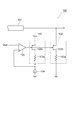
(第1の実施の形態)
図1は、本発明に係る受信回路の第1実施形態の構成を示す回路図である。同図に示す受信回路1aは、差動信号SDを受信する回路であって、差動信号SDのうち正相信号SPを外部から受信する第1の端子2と、差動信号SDのうち逆相信号SNを外部から受信する第2の端子3と、正相信号SP及び逆相信号SNを増幅して受信信号Sinを生成する増幅器4と、端子2及び増幅器4を互いに結ぶ信号ライン5、並びに端子3及び増幅器4を互いに結ぶ信号ライン6を終端するための終端回路7とを備える。なお、本実施形態の受信回路1aは、一つのICチップ内に集積されることが好ましい。
(First embodiment)
FIG. 1 is a circuit diagram showing a configuration of a first embodiment of a receiving circuit according to the present invention. The
終端回路7は、第1の抵抗11a、第2の抵抗11b、第3の抵抗11c、及び第4の抵抗11dと、トランジスタ12a及び12bと、定電流源13と、制御電圧生成部14とを有する。抵抗11a〜11dは、例えばICチップ内に形成されたシート抵抗によって構成されている。
The
抵抗11a及び11bは、第1の端子2と第2の端子3との間(本実施形態では、信号ライン5と信号ライン6との間)に直列に接続されており、第1の端子2と第2の端子3との間の終端抵抗として機能する。抵抗11a及び11bの抵抗値は、互いに同じ値となっている。従って、抵抗11a及び11bの相互接続点Aにおける電位Vmonは、第1の端子2及び第2の端子3の中間の電位となる。なお、第1の端子2及び第2の端子3へ入力されるのが差動信号SD(正相信号SP、逆相信号SN)なので、相互接続点Aの電位Vmonは差動信号SDの状態には殆ど影響されない。
The
トランジスタ12aは、本実施形態における第1のトランジスタであり、第1の端子2と第1の定電位線(正の電源電位線Vcc)との間の可変終端抵抗素子として設けられている。具体的には、トランジスタ12aの一方の電流端子(ドレイン)は信号ライン5に接続されており、他方の電流端子(ソース)は電源電位線Vccに接続されている。本実施形態では抵抗11cがトランジスタ12aに対し直列に接続されており、トランジスタ12aの一方の電流端子(ドレイン)は抵抗11cを介して信号ライン5に接続されている。従って、第1の端子2は、トランジスタ12a及び抵抗11cによって終端される。
The
トランジスタ12bは、本実施形態における第2のトランジスタであり、第2の端子3と第1の定電位線(正の電源電位線Vcc)との間の可変終端抵抗素子として設けられている。具体的には、トランジスタ12bの一方の電流端子(ドレイン)は信号ライン6に接続されている。また、トランジスタ12bの他方の電流端子(ソース)は電源電位線Vccに接続されており、トランジスタ12aの他方の電流端子(ソース)と共通電位となっている。本実施形態では、抵抗11cと等しい抵抗値を有する抵抗11dがトランジスタ12bに対し直列に接続されており、トランジスタ12bの一方の電流端子(ドレイン)は抵抗11dを介して信号ライン6に接続されている。従って、第2の端子3は、トランジスタ12b及び抵抗11dによって終端される。
The
トランジスタ12a及び12bは、そのゲート長やゲート幅といった寸法が互いに等しくなるようにICチップ内に形成されている。また、図1にはトランジスタ12a,12bとしてnチャネルMOS型FETを図示しているが、他のタイプのFETやバイポーラトランジスタを代わりに用いてもよい。また、抵抗11c及び11dは、トランジスタ12a及び12bの他方の電流端子(ソース)側に接続されてもよい。
The
定電流源13は、電源電位線Vccとは電位が異なる第2の定電位線(本実施形態では接地電位線GND)と抵抗11a及び11bの相互接続点Aとの間に接続されており、接地電位線GNDと相互接続点Aとの間に所定の大きさの定電流I1を流す。本実施形態の終端回路7においては、トランジスタ12a、抵抗11a及び11cからなる直列抵抗成分と、トランジスタ12b、抵抗11b及び11dからなる直列抵抗成分とが、電源電位線Vccと相互接続点Aとの間で並列に接続されており、これらの直列抵抗成分の抵抗値は実質的に等しく設定されている。従って、トランジスタ12a、抵抗11a及び11cを流れる電流I2の大きさ、並びにトランジスタ12b、抵抗11b及び11dを流れる電流I3の大きさは、それぞれ定電流I1の1/2となる。なお、定電流I1の大きさは、受信回路1aの温度や電源電圧Vccの大きさに依らず一定であることが好ましい。
The constant
制御電圧生成部14は、トランジスタ12a及び12bの各制御端子(ゲート)に制御電圧Vgを提供する。制御電圧生成部14は、抵抗11a及び11bの相互接続点Aの電位Vmonを入力し、この電位Vmonが所定電位に近づくように制御電圧Vgを生成する。本実施形態の制御電圧生成部14は、差動増幅器15を含む。差動増幅器15の非反転入力端は相互接続点Aに接続されており、反転入力端は参照電圧Vrefを発生する定電圧源16に接続されている。差動増幅器15は、相互接続点Aの電位Vmonと参照電圧Vrefとの電位差を増幅し、制御電圧Vgとしてトランジスタ12a及び12bへ出力する。トランジスタ12a及び12bのドレイン−ソース間抵抗は、この制御電圧Vgが高くなると減少し、低くなると増加する。
The
以上の構成を備える受信回路1aの作用及び効果について説明する。いま、第1の端子2と第2の端子3との間を終端する抵抗11a及び11bの抵抗値をそれぞれRab/2とし、トランジスタ12a及び抵抗11cからなる直列抵抗値をRacとし、トランジスタ12b及び抵抗11dからなる直列抵抗値をRbc(=Rac)とする。この場合、相互接続点Aと電源電位線Vccとの間の抵抗値Rxは、
と表される。
The operation and effect of the receiving
It is expressed.
端子2,3へ入力される信号が差動信号であれば相互接続点Aは仮想接地点となるので、相互接続点Aの電位Vmonに対する受信信号の影響は殆ど無い。従って、トランジスタ12a及び抵抗11a,11cを流れる電流I2、並びにトランジスタ12b及び抵抗11b,11dを流れる電流I3による電圧降下によって相互接続点Aの電位Vmonが定まる。換言すれば、相互接続点Aの電位Vmonは、トランジスタ12a,12bの電流端子間(ソース−ドレイン間)の抵抗値を反映した値となる。終端回路7においては、この電位Vmonと参照電圧Vrefとの差を差動増幅器15により増幅し、差動増幅器15の出力を制御電圧Vgとしてトランジスタ12a,12bの制御端子(ゲート)に帰還させることによって、抵抗値Rac,Rbcの自動制御を実現している。
If the signal input to the
参照電圧Vrefは、電源電位線Vccの電位から目標電圧Vtgtを差し引いた電圧を供給する。目標電圧Vtgtは、抵抗値Rx及び定電流I1の積とほぼ同値になるよう設定される。 As the reference voltage Vref, a voltage obtained by subtracting the target voltage Vtgt from the potential of the power supply potential line Vcc is supplied. The target voltage Vtgt is set to be substantially the same value as the product of the resistance value Rx and the constant current I1.
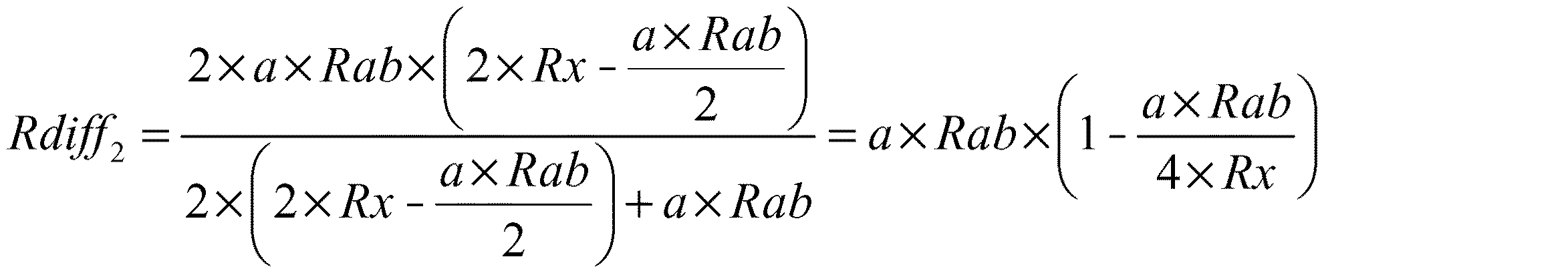
ここで、終端回路7による終端抵抗値Rdiffは、Δ−Y変換公式から
と表される。抵抗値のプロセス変動率(製造誤差)をa(例えば0.7≦a≦1.3、変動無しのとき1.0)とおき、抵抗値Rac及びRdiffにプロセス変動を加味した値をそれぞれRac2及びRdiff2とすると、(2)式は、
となる。本実施形態の終端回路7においては、差動増幅器15による帰還制御によって、抵抗値Rxがプロセス変動に依らず一定となるように制御される。従って、Rac2は、
と表される。(4)式を(3)式に代入すると、
となる。なお、(5)式からわかるように、或る抵抗値Rdiff2を実現するための抵抗値Rab及びRxの組み合わせは複数存在する。従って、例えば差動伝送における一般的な特性インピーダンスである100Ωに抵抗値Rdiff2を設定する場合においても、抵抗値Rab及びRxの任意の組み合わせによってその抵抗値を実現できる。
Here, the termination resistance value Rdiff by the
It is expressed. The process variation rate (manufacturing error) of the resistance value is set to a (for example, 0.7 ≦ a ≦ 1.3, 1.0 when there is no variation), and values obtained by adding process variation to the resistance values Rac and Rdiff are respectively Rac. 2 and Rdiff 2 , the equation (2) is
It becomes. In the
It is expressed. Substituting equation (4) into equation (3),
It becomes. Incidentally, (5) As can be seen from the equation, the combination of the resistance value Rab and Rx for realizing a certain resistance value Rdiff 2 there are a plurality. Therefore, for example, even when the resistance value Rdiff 2 is set to 100Ω, which is a general characteristic impedance in differential transmission, the resistance value can be realized by any combination of the resistance values Rab and Rx.
図2は、プロセス変動を加味した差動入力抵抗値(終端抵抗値)Rdiff2と、プロセス変動率aとの関係((5)式参照)を示している。図2において、グラフG1はRab=200[Ω]、Rx=100[Ω]としたものであり、グラフG2はRab=204[Ω]、Rx=102[Ω]としたものであり、グラフG3はRab=150[Ω]、Rx=112.5[Ω]としたものである。なお、グラフG4は、比較のため、集積回路のシート抵抗のみで終端抵抗を構成した場合を示している。 FIG. 2 shows the relationship between the differential input resistance value (termination resistance value) Rdiff 2 taking into account the process variation and the process variation rate a (see equation (5)). In FIG. 2, a graph G1 is obtained with Rab = 200 [Ω] and Rx = 100 [Ω], and a graph G2 is obtained with Rab = 204 [Ω] and Rx = 102 [Ω]. Are Rab = 150 [Ω] and Rx = 112.5 [Ω]. For comparison, graph G4 shows a case where the termination resistor is configured only by the sheet resistance of the integrated circuit.
グラフG1〜G3を参照すると、グラフG4と比較してプロセス変動による終端抵抗値の変動幅が効果的に狭められていることがわかる。すなわち、グラフG1の場合、0.7≦a≦1.3のプロセス変動に対して終端抵抗値の変動幅が設計値(100Ω)の10%以下であり、プロセス変動による終端抵抗値の変動が極めて効果的に抑えられている。また、グラフG2の場合、0.7≦a≦1.3のプロセス変動に対して終端抵抗値の変動範囲が102Ωを頂点として変化しており、プロセス変動がゼロの場合に終端抵抗値が誤差を含んでしまうが、終端抵抗値の変動幅に関してはグラフG1と同様に小さく抑えられている。また、グラフG3の場合、グラフG1及びG2の場合と比較してその効果は小さいが、従来型(グラフG4)と比較して終端抵抗値の変動幅を小さく抑えることができる。 Referring to the graphs G1 to G3, it can be seen that the variation range of the termination resistance value due to the process variation is effectively narrowed compared to the graph G4. That is, in the case of the graph G1, the variation width of the termination resistance value is 10% or less of the design value (100Ω) with respect to the process variation of 0.7 ≦ a ≦ 1.3. It is very effectively suppressed. In the case of the graph G2, the variation range of the termination resistance value changes with 102Ω as the apex with respect to the process variation of 0.7 ≦ a ≦ 1.3, and when the process variation is zero, the termination resistance value is an error. However, the fluctuation range of the termination resistance value is kept small as in the graph G1. Further, in the case of the graph G3, the effect is small compared to the cases of the graphs G1 and G2, but the fluctuation range of the termination resistance value can be suppressed to be small compared to the conventional type (graph G4).
また、図3は、受信回路1aにおけるリターンロス[dB]とプロセス変動率aとの関係を示している。図3において、グラフG5〜G8は、それぞれ図2のグラフG1〜G4に対応している。なお、リターンロスLOSS[dB]は、次の(6)式によって算出される。(6)式において、Z0は特性インピーダンスであり、Ziは実際の終端抵抗値(図2における縦軸の値)である。
図3に示すように、グラフG6の場合(すなわちRab=204[Ω]、Rx=102[Ω])では、0.8≦a≦1.2のプロセス変動に対してほぼ−40dB以下のリターンロスを確保できることがわかる。また、グラフG5(Rab=200[Ω]、Rx=100[Ω])の場合、及びグラフG7の場合(Rab=150[Ω]、Rx=112.5[Ω])においても、従来型(グラフG8)と比較してリターンロスが少なくとも0.7≦a≦1.3の範囲で低下していることがわかる。
FIG. 3 shows the relationship between the return loss [dB] and the process variation rate a in the receiving
As shown in FIG. 3, in the case of the graph G6 (that is, Rab = 204 [Ω], Rx = 102 [Ω]), a return of approximately −40 dB or less with respect to a process variation of 0.8 ≦ a ≦ 1.2. It can be seen that loss can be secured. In the case of the graph G5 (Rab = 200 [Ω], Rx = 100 [Ω]) and the graph G7 (Rab = 150 [Ω], Rx = 112.5 [Ω]), the conventional type ( It can be seen that the return loss is reduced in the range of at least 0.7 ≦ a ≦ 1.3 compared to graph G8).
本実施形態の受信回路1aの作用効果を端的に述べると、以下のとおりである。受信回路1aにおいては、相互接続点Aの電位Vmonが、トランジスタ12aの電流端子間(ソース−ドレイン間)抵抗、及び抵抗11a,11cからなる直列抵抗値と、トランジスタ12bの電流端子間抵抗、及び抵抗11b,11dからなる直列抵抗値とを反映した値となる。受信回路1aでは、この電位Vmonが所定電位に近づくように制御電圧生成部14(差動増幅器15)がトランジスタ12a,12bへ制御電圧Vgを提供するので、トランジスタ12a,12bの電流端子間の抵抗値が制御され、上記した直列抵抗値が或る所定値に精度良く制御される。このように、本実施形態の受信回路1aによれば、図5に示した回路とは異なり終端抵抗部分が帰還回路に含まれるので、トランジスタや抵抗素子の誤差、或いは信号ラインの電圧変動に関わらず、精度が高い終端回路7を実現することができる。
The operational effects of the receiving
また、本実施形態のように、終端回路7は、トランジスタ12a,12bのそれぞれに直列接続された抵抗11c,11dを備えることが好ましい。これにより、第1の端子2の終端抵抗がトランジスタ12a及び抵抗11cによって構成され、第2の端子3の終端抵抗がトランジスタ12b及び抵抗11dによって構成されるので、終端抵抗値の可変幅を更に狭くして終端抵抗値をより高精度に制御できる。
Further, as in the present embodiment, the
なお、終端回路7の高周波特性に関しては、トランジスタ12a,12bの寸法に依存する。Rxを100Ω、Rabを200Ωに設定した場合、Rac及びRbcはそれぞれ100Ωとなるが、プロセス変動に対するトランジスタ12a,12bの抵抗値の制御範囲を考慮してRac,Rbcの1/2の抵抗値をトランジスタ12a,12bに割り当てた場合、トランジスタ12a,12bに要求される電流端子間抵抗は50Ωとなる。これに対し、図5に示した終端回路100は片相終端回路なので、同様の終端条件(差動で100Ω、片相で50Ω)を実現しようとした場合、同様に50Ωの1/2の抵抗値をトランジスタに割り当てると、トランジスタに要求される電流端子間抵抗は25Ωとなり、更に小さくなってしまう。
The high-frequency characteristics of the
ここで、例えばMOS型FETの深い三極管領域における電流端子間抵抗値Rmosは、
と表される。(7)式において、μは電子の移動度、COXはゲート絶縁層の容量、Wはゲート幅、Lはゲート長、Vgsはゲート−ソース間電圧、VthはMOS型FETのしきい値電圧である。(7)式より、電流端子間抵抗値を小さくする為には、W/Lを大きくする必要がある(プロセス条件は同一)。しかしながら、W/Lを大きくすると各端子における寄生容量が大きくなってしまい、高周波特性を劣化させることとなる。このことから、本実施形態の終端回路7は、図5に示した従来の終端回路100と比較して高周波特性に優れており、受信回路1aに特に好適であることがわかる。
Here, for example, the resistance value Rmos between current terminals in the deep triode region of the MOS FET is:
It is expressed. In Equation (7), μ is the mobility of electrons, C OX is the capacitance of the gate insulating layer, W is the gate width, L is the gate length, Vgs is the gate-source voltage, and Vth is the threshold voltage of the MOS FET. It is. From equation (7), in order to reduce the resistance value between the current terminals, it is necessary to increase W / L (the process conditions are the same). However, when W / L is increased, the parasitic capacitance at each terminal is increased and the high frequency characteristics are deteriorated. From this, it can be seen that the
(第2の実施の形態)
図4は、本発明に係る受信回路の第2実施形態の構成を示す回路図である。同図に示す受信回路1bは、第1の端子2及び第2の端子3、増幅器4、及び終端回路8を備える。なお、これらのうち、終端回路8を除く他の構成については上記第1実施形態と同様なので詳細な説明を省略する。
(Second Embodiment)
FIG. 4 is a circuit diagram showing a configuration of a second embodiment of the receiving circuit according to the present invention. The receiving
終端回路8は、第1実施形態と同様に構成された第1の抵抗11a及び第2の抵抗11bを有する。また、終端回路8は、第1実施形態とは異なる構成の第3の抵抗11e及び第4の抵抗11f、トランジスタ12c及び12d、定電流源17、並びに制御電圧生成部18を有する。
The termination circuit 8 includes a
トランジスタ12cは、本実施形態における第1のトランジスタであり、第1の端子2と第1の定電位線(本実施形態では接地電位線GNDが第1の定電位線となっている)との間の可変終端抵抗素子として設けられている。具体的には、トランジスタ12cの一方の電流端子(ソース)は信号ライン5に接続されており、他方の電流端子(ドレイン)は接地電位線GNDに接続されている。本実施形態では抵抗11eがトランジスタ12cに対し直列に接続されており、トランジスタ12cの他方の電流端子(ドレイン)は抵抗11eを介して接地電位線GNDに接続されている。従って、第1の端子2は、トランジスタ12c及び抵抗11eによって終端される。
The
トランジスタ12dは、本実施形態における第2のトランジスタであり、第2の端子3と第1の定電位線(接地電位線GND)との間の可変終端抵抗素子として設けられている。具体的には、トランジスタ12dの一方の電流端子(ソース)は信号ライン6に接続されており、他方の電流端子(ドレイン)は接地電位線GNDに接続されている。本実施形態では、抵抗11eと等しい抵抗値を有する抵抗11fがトランジスタ12dに対し直列に接続されており、トランジスタ12dの他方の電流端子(ドレイン)は抵抗11fを介して接地電位線GNDに接続されている。従って、第2の端子3は、トランジスタ12d及び抵抗11fによって終端される。
The
なお、トランジスタ12c及び12dは、そのゲート長やゲート幅といった寸法が互いに等しくなるようにICチップ内に形成されている。また、図4にはトランジスタ12c,12dとしてnチャネルMOS型FETを図示しているが、他のタイプのFETやバイポーラトランジスタを代わりに用いてもよい。また、抵抗11e及び11dは、トランジスタ12c及び12dの一方の電流端子(ソース)側に接続されてもよい。
The
定電流源17は、接地電位線GNDとは電位が異なる第2の定電位線(本実施形態では正の電源電位線Vcc)と相互接続点Aとの間に接続されており、電源電位線Vccと相互接続点Aとの間に所定の大きさの定電流I4を流す。本実施形態の終端回路8においては、トランジスタ12c、抵抗11a及び11eからなる直列抵抗成分と、トランジスタ12d、抵抗11b及び11fからなる直列抵抗成分とが、相互接続点Aと接地電位線GNDとの間で並列に接続されており、これらの直列抵抗成分の抵抗値は実質的に等しく設定されている。従って、トランジスタ12c、抵抗11a及び11eを流れる電流I5の大きさ、並びにトランジスタ12d、抵抗11b及び11fを流れる電流I6の大きさは、それぞれ定電流I4の1/2となる。なお、定電流I4の大きさは、受信回路1bの温度や電源電圧Vccの大きさに依らず一定であることが好ましい。
The constant
制御電圧生成部18は、トランジスタ12c及び12dの各制御端子(ゲート)に制御電圧Vgを提供する。制御電圧生成部18は、相互接続点Aの電位Vmonを入力し、この電位Vmonが所定電位に近づくように制御電圧Vgを生成する。本実施形態の制御電圧生成部18は、差動増幅器19を含む。差動増幅器19の非反転入力端は相互接続点Aに接続されており、反転入力端は参照電圧Vrefを発生する定電圧源20に接続されている。差動増幅器19は、相互接続点Aの電位Vmonと参照電圧Vrefとの電位差を増幅し、制御電圧Vgとしてトランジスタ12c及び12dへ出力する。トランジスタ12c及び12dのドレイン−ソース間抵抗は、この制御電圧Vgが高くなると減少し、低くなると増加する。
The
本実施形態の受信回路1bの作用効果について説明する。受信回路1bにおいては、トランジスタ12c及び抵抗11eが第1の端子2の終端抵抗として機能しており、トランジスタ12d及び抵抗11fが第2の端子3の終端抵抗として機能している。この受信回路1bにおいては、トランジスタ12c、抵抗11a及び11eからなる直列抵抗成分と、トランジスタ12d、抵抗11b及び11fからなる直列抵抗成分とが、第1の定電位線(接地電位線GND)と相互接続点Aとの間で並列に接続されている。従って、この並列抵抗回路に定電流I4が流れる際の電圧降下に相当する電位が、相互接続点Aの電位Vmonとなる。
The effect of the receiving
すなわち、相互接続点Aの電位Vmonは、トランジスタ12cの電流端子間(ソース−ドレイン間)抵抗、及び抵抗11a,11eからなる直列抵抗値と、トランジスタ12dの電流端子間抵抗、及び抵抗11b,11fからなる直列抵抗値とを反映した値となる。受信回路1bでは、この電位Vmonが所定電位に近づくように制御電圧生成部18(差動増幅器19)がトランジスタ12c,12dへ制御電圧Vgを提供するので、トランジスタ12c,12dの電流端子間の抵抗値が制御され、上記した直列抵抗値が或る所定値に精度良く制御される。このように、本実施形態の受信回路1bによれば、終端抵抗部分が帰還回路に含まれるので、トランジスタや抵抗素子の誤差、或いは信号ラインの電圧変動に関わらず、精度が高い終端回路8を実現することができる。
That is, the potential Vmon at the interconnection point A is the resistance between the current terminals (source-drain) of the
本発明による受信回路は、上記した実施形態に限られるものではなく、他に様々な変形が可能である。例えば、上記実施形態においては第1及び第2の定電位線をそれぞれ電源電位線及び接地電位線(またはその逆)としているが、互いに電位が異なる定電位線であれば、これらに限られるものではない。また、上記実施形態において、第1及び第2のトランジスタ、第1〜第4の抵抗等は一つのICチップ内に形成されると説明したが、本発明において、これらは個別の部品として存在してもよい。 The receiving circuit according to the present invention is not limited to the above-described embodiment, and various other modifications are possible. For example, in the above embodiment, the first and second constant potential lines are the power supply potential line and the ground potential line (or vice versa), respectively, but the constant potential lines are different as long as they are constant potential lines having different potentials. is not. In the above embodiment, the first and second transistors, the first to fourth resistors, and the like have been described as being formed in one IC chip. However, in the present invention, these exist as individual components. May be.
1a,1b…受信回路、2…第1の端子、3…第2の端子、4…増幅器、5,6…信号ライン、7,8…終端回路、11a〜11f…抵抗、12a〜12d…トランジスタ、13,17…定電流源、14,18…制御電圧生成部、15,19…差動増幅器、16,20…定電圧源、A…相互接続点、SD…差動信号、SN…逆相信号、SP…正相信号、Vg…制御電圧。
DESCRIPTION OF
Claims (4)
前記差動信号の正相信号を受ける第1の端子及び逆相信号を受ける第2の端子と、
前記第1の端子と前記第2の端子との間に直列に接続され互いに等しい抵抗値を有する第1及び第2の抵抗と、
一方の電流端子が前記第1の端子に接続され、他方の電流端子が第1の定電位線に接続された第1のトランジスタと、
一方の電流端子が前記第2の端子に接続され、他方の電流端子が前記第1の定電位線に接続された第2のトランジスタと、
前記第1の定電位線とは電位が異なる第2の定電位線と前記第1及び第2の抵抗の相互接続点との間に接続された定電流源と、
前記第1及び第2のトランジスタの各制御端子に、前記相互接続点の電位が所定電位に近づくような制御電圧を提供する制御電圧生成部と
を備え、
前記所定電位は、前記第1のトランジスタ及び前記第2のトランジスタの動作抵抗Rxと、前記第1及び前記第2の抵抗が直列に接続された時の抵抗値Rabとが、以下の式
A first terminal for receiving a positive phase signal of the differential signal and a second terminal for receiving a negative phase signal;
A first resistor and a second resistor connected in series between the first terminal and the second terminal and having equal resistance values ;
A first transistor having one current terminal connected to the first terminal and the other current terminal connected to a first constant potential line;
A second transistor having one current terminal connected to the second terminal and the other current terminal connected to the first constant potential line;
A constant current source connected between a second constant potential line having a different potential from the first constant potential line and an interconnection point of the first and second resistors;
A control voltage generator for providing a control voltage at each control terminal of the first and second transistors so that the potential at the interconnection point approaches a predetermined potential ;
The predetermined potential is determined by the following equation: an operating resistance Rx of the first transistor and the second transistor, and a resistance value Rab when the first and second resistors are connected in series.
Priority Applications (2)
| Application Number | Priority Date | Filing Date | Title |
|---|---|---|---|
| JP2007062404A JP4876987B2 (en) | 2007-03-12 | 2007-03-12 | Receiver circuit |
| US12/073,571 US7843212B2 (en) | 2007-03-12 | 2008-03-06 | Differential circuit with precisely controlled terminator circuit |
Applications Claiming Priority (1)
| Application Number | Priority Date | Filing Date | Title |
|---|---|---|---|
| JP2007062404A JP4876987B2 (en) | 2007-03-12 | 2007-03-12 | Receiver circuit |
Publications (2)
| Publication Number | Publication Date |
|---|---|
| JP2008227857A JP2008227857A (en) | 2008-09-25 |
| JP4876987B2 true JP4876987B2 (en) | 2012-02-15 |
Family
ID=39794580
Family Applications (1)
| Application Number | Title | Priority Date | Filing Date |
|---|---|---|---|
| JP2007062404A Active JP4876987B2 (en) | 2007-03-12 | 2007-03-12 | Receiver circuit |
Country Status (2)
| Country | Link |
|---|---|
| US (1) | US7843212B2 (en) |
| JP (1) | JP4876987B2 (en) |
Families Citing this family (6)
| Publication number | Priority date | Publication date | Assignee | Title |
|---|---|---|---|---|
| US7439760B2 (en) | 2005-12-19 | 2008-10-21 | Rambus Inc. | Configurable on-die termination |
| GB2486274A (en) * | 2010-12-10 | 2012-06-13 | Microsemi Semiconductor Corp | A programmable bias circuit for the centre node of a balanced receiver termination circuit |
| US9231731B1 (en) * | 2012-04-06 | 2016-01-05 | Rambus Inc. | Common mode calibration |
| CN103199839A (en) * | 2013-02-22 | 2013-07-10 | 刘德志 | Light-operated anti-theft device |
| US8994399B2 (en) * | 2013-04-29 | 2015-03-31 | Broadcom Corporation | Transmission line driver with output swing control |
| JP6582640B2 (en) * | 2015-07-07 | 2019-10-02 | 住友電気工業株式会社 | Laser drive circuit |
Family Cites Families (21)
| Publication number | Priority date | Publication date | Assignee | Title |
|---|---|---|---|---|
| NL8901170A (en) * | 1989-05-10 | 1990-12-03 | Philips Nv | INTEGRATED CIRCUIT WITH A SIGNAL LEVEL CONVERTER. |
| SE9400657D0 (en) * | 1994-02-25 | 1994-02-25 | Ellemtel Utvecklings Ab | One, a control voltage generating, circuit |
| DE4445846A1 (en) * | 1994-12-22 | 1996-06-27 | Sel Alcatel Ag | Method and circuit arrangement for the termination of a line leading to an integrated CMOS circuit |
| TW381218B (en) * | 1998-04-20 | 2000-02-01 | Via Tech Inc | I/O buffer for improving ring back effect |
| JP3420735B2 (en) * | 1999-04-06 | 2003-06-30 | 松下電器産業株式会社 | Constant current output circuit |
| US6424169B1 (en) * | 2000-01-24 | 2002-07-23 | Broadcom Corporation | Active termination network |
| US6414512B1 (en) * | 2000-04-04 | 2002-07-02 | Pixelworks, Inc. | On-chip termination circuit |
| US6605958B2 (en) * | 2000-10-11 | 2003-08-12 | Vitesse Semiconductor Corporation | Precision on-chip transmission line termination |
| KR100410536B1 (en) * | 2001-02-05 | 2003-12-18 | 삼성전자주식회사 | Impedance update apparatus and method of termination circuit |
| US7102200B2 (en) * | 2001-09-04 | 2006-09-05 | Intel Corporation | On-die termination resistor with analog compensation |
| JP2003298395A (en) * | 2002-04-04 | 2003-10-17 | Mitsubishi Electric Corp | Differential terminating resistance adjusting circuit |
| US6836142B2 (en) * | 2002-07-12 | 2004-12-28 | Xilinx, Inc. | Asymmetric bidirectional bus implemented using an I/O device with a digitally controlled impedance |
| US6664814B1 (en) * | 2002-07-18 | 2003-12-16 | Cadence Design Systems, Inc. | Output driver for an integrated circuit |
| US6909305B1 (en) * | 2003-08-08 | 2005-06-21 | Ami Semiconductor, Inc. | Digitally controlled impedance driver matching for wide voltage swings at input/output node and having programmable step size |
| TWI304529B (en) * | 2004-01-30 | 2008-12-21 | Realtek Semiconductor Corp | Impedance control circuit and method thereof |
| JP2006060320A (en) * | 2004-08-17 | 2006-03-02 | Sony Corp | Circuit and method for differential signal driving |
| US7230449B2 (en) * | 2005-02-11 | 2007-06-12 | International Business Machines Corporation | Data receiver with a programmable reference voltage to optimize timing jitter |
| US7375575B1 (en) * | 2005-02-14 | 2008-05-20 | Marvell Israel (Misl) Ltd. | Method and apparatus for controlled voltage level shifting |
| JP2007028330A (en) * | 2005-07-19 | 2007-02-01 | Nec Electronics Corp | Semiconductor circuit and resistance value control method |
| JP4869667B2 (en) * | 2005-09-29 | 2012-02-08 | ローム株式会社 | Differential signal transmitter circuit and electronic device using the same |
| US7391231B2 (en) * | 2006-06-19 | 2008-06-24 | International Business Machines Corporation | Switch selectable terminator for differential and pseudo-differential signaling |
-
2007
- 2007-03-12 JP JP2007062404A patent/JP4876987B2/en active Active
-
2008
- 2008-03-06 US US12/073,571 patent/US7843212B2/en active Active
Also Published As
| Publication number | Publication date |
|---|---|
| JP2008227857A (en) | 2008-09-25 |
| US20080240739A1 (en) | 2008-10-02 |
| US7843212B2 (en) | 2010-11-30 |
Similar Documents
| Publication | Publication Date | Title |
|---|---|---|
| JP4876987B2 (en) | Receiver circuit | |
| US7619448B2 (en) | Replica bias circuit for high speed low voltage common mode driver | |
| US6504404B2 (en) | Semiconductor integrated circuit | |
| US9966908B1 (en) | Circuit for and method of implementing a differential input receiver | |
| US7940036B2 (en) | Voltage comparison circuit, and semiconductor integrated circuit and electronic device having the same | |
| US6756812B2 (en) | Differential termination resistor adjusting circuit | |
| US7733181B2 (en) | Amplifier circuit having dynamically biased configuration | |
| US8884655B2 (en) | Low-power voltage mode high speed driver | |
| US7825699B2 (en) | Receiver circuit having compensated offset voltage | |
| US7633346B2 (en) | Transconductance compensating bias circuit and amplifier | |
| US8022764B2 (en) | Differential amplifier | |
| US20120001663A1 (en) | Mixed-mode input buffer | |
| WO2005050834A1 (en) | Am intermediate frequency variable gain amplifier circuit, variable gain amplifier circuit, and semiconductor integrated circuit thereof | |
| US20090091357A1 (en) | Low voltage differential signalling driver | |
| US20120188016A1 (en) | Circuitry for biasing amplifiers | |
| EP1804375B1 (en) | Differential amplifier circuit operable with wide range of input voltages | |
| JP2009278526A (en) | Semiconductor integrated circuit device | |
| US8723600B1 (en) | Cancellation of dynamic offset in MOS resistors | |
| JP5126355B2 (en) | Termination circuit, semiconductor device, and electronic device | |
| US20150280663A1 (en) | Semiconductor circuit and amplifier circuit | |
| JP3784382B2 (en) | Semiconductor integrated circuit | |
| JP6306413B2 (en) | Regulator circuit | |
| JP2009171338A (en) | Attenuation compensating circuit | |
| JP4332522B2 (en) | Differential amplifier circuit | |
| JP5126221B2 (en) | Amplifier circuit |
Legal Events
| Date | Code | Title | Description |
|---|---|---|---|
| A621 | Written request for application examination |
Free format text: JAPANESE INTERMEDIATE CODE: A621 Effective date: 20100218 |
|
| A977 | Report on retrieval |
Free format text: JAPANESE INTERMEDIATE CODE: A971007 Effective date: 20110527 |
|
| A131 | Notification of reasons for refusal |
Free format text: JAPANESE INTERMEDIATE CODE: A131 Effective date: 20110531 |
|
| A521 | Request for written amendment filed |
Free format text: JAPANESE INTERMEDIATE CODE: A523 Effective date: 20110727 |
|
| TRDD | Decision of grant or rejection written | ||
| A01 | Written decision to grant a patent or to grant a registration (utility model) |
Free format text: JAPANESE INTERMEDIATE CODE: A01 Effective date: 20111101 |
|
| A01 | Written decision to grant a patent or to grant a registration (utility model) |
Free format text: JAPANESE INTERMEDIATE CODE: A01 |
|
| A61 | First payment of annual fees (during grant procedure) |
Free format text: JAPANESE INTERMEDIATE CODE: A61 Effective date: 20111114 |
|
| R150 | Certificate of patent or registration of utility model |
Ref document number: 4876987 Country of ref document: JP Free format text: JAPANESE INTERMEDIATE CODE: R150 Free format text: JAPANESE INTERMEDIATE CODE: R150 |
|
| FPAY | Renewal fee payment (event date is renewal date of database) |
Free format text: PAYMENT UNTIL: 20141209 Year of fee payment: 3 |
|
| R250 | Receipt of annual fees |
Free format text: JAPANESE INTERMEDIATE CODE: R250 |
|
| R250 | Receipt of annual fees |
Free format text: JAPANESE INTERMEDIATE CODE: R250 |
|
| R250 | Receipt of annual fees |
Free format text: JAPANESE INTERMEDIATE CODE: R250 |
|
| R250 | Receipt of annual fees |
Free format text: JAPANESE INTERMEDIATE CODE: R250 |
|
| R250 | Receipt of annual fees |
Free format text: JAPANESE INTERMEDIATE CODE: R250 |
|
| R250 | Receipt of annual fees |
Free format text: JAPANESE INTERMEDIATE CODE: R250 |
|
| R250 | Receipt of annual fees |
Free format text: JAPANESE INTERMEDIATE CODE: R250 |
|
| R250 | Receipt of annual fees |
Free format text: JAPANESE INTERMEDIATE CODE: R250 |
|
| R250 | Receipt of annual fees |
Free format text: JAPANESE INTERMEDIATE CODE: R250 |
|
| R250 | Receipt of annual fees |
Free format text: JAPANESE INTERMEDIATE CODE: R250 |