JP4827618B2 - アンテナの作製方法、半導体装置の作製方法 - Google Patents
アンテナの作製方法、半導体装置の作製方法 Download PDFInfo
- Publication number
- JP4827618B2 JP4827618B2 JP2006149782A JP2006149782A JP4827618B2 JP 4827618 B2 JP4827618 B2 JP 4827618B2 JP 2006149782 A JP2006149782 A JP 2006149782A JP 2006149782 A JP2006149782 A JP 2006149782A JP 4827618 B2 JP4827618 B2 JP 4827618B2
- Authority
- JP
- Japan
- Prior art keywords
- conductive film
- film
- opening
- antenna
- substrate
- Prior art date
- Legal status (The legal status is an assumption and is not a legal conclusion. Google has not performed a legal analysis and makes no representation as to the accuracy of the status listed.)
- Expired - Fee Related
Links
Images


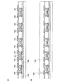

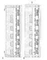


Landscapes
- Electrodes Of Semiconductors (AREA)
- Internal Circuitry In Semiconductor Integrated Circuit Devices (AREA)
- Semiconductor Integrated Circuits (AREA)
- Thin Film Transistor (AREA)
- Details Of Aerials (AREA)
Priority Applications (1)
| Application Number | Priority Date | Filing Date | Title |
|---|---|---|---|
| JP2006149782A JP4827618B2 (ja) | 2005-05-31 | 2006-05-30 | アンテナの作製方法、半導体装置の作製方法 |
Applications Claiming Priority (3)
| Application Number | Priority Date | Filing Date | Title |
|---|---|---|---|
| JP2005160192 | 2005-05-31 | ||
| JP2005160192 | 2005-05-31 | ||
| JP2006149782A JP4827618B2 (ja) | 2005-05-31 | 2006-05-30 | アンテナの作製方法、半導体装置の作製方法 |
Publications (3)
| Publication Number | Publication Date |
|---|---|
| JP2007012042A JP2007012042A (ja) | 2007-01-18 |
| JP2007012042A5 JP2007012042A5 (cg-RX-API-DMAC10.html) | 2009-05-14 |
| JP4827618B2 true JP4827618B2 (ja) | 2011-11-30 |
Family
ID=37750379
Family Applications (1)
| Application Number | Title | Priority Date | Filing Date |
|---|---|---|---|
| JP2006149782A Expired - Fee Related JP4827618B2 (ja) | 2005-05-31 | 2006-05-30 | アンテナの作製方法、半導体装置の作製方法 |
Country Status (1)
| Country | Link |
|---|---|
| JP (1) | JP4827618B2 (cg-RX-API-DMAC10.html) |
Families Citing this family (13)
| Publication number | Priority date | Publication date | Assignee | Title |
|---|---|---|---|---|
| US8816484B2 (en) * | 2007-02-09 | 2014-08-26 | Semiconductor Energy Laboratory Co., Ltd. | Semiconductor device |
| EP2372756A1 (en) | 2007-03-13 | 2011-10-05 | Semiconductor Energy Laboratory Co, Ltd. | Semiconductor device and manufacturing method thereof |
| JP5150618B2 (ja) * | 2007-03-29 | 2013-02-20 | パナソニック株式会社 | アンテナ装置及び携帯端末機器 |
| EP1978472A3 (en) * | 2007-04-06 | 2015-04-22 | Semiconductor Energy Laboratory Co., Ltd. | Semiconductor device and method for manufacturing the same |
| JP4997007B2 (ja) * | 2007-07-19 | 2012-08-08 | トッパン・フォームズ株式会社 | Rf−idメディア及びその製造方法 |
| JP5306705B2 (ja) * | 2008-05-23 | 2013-10-02 | 株式会社半導体エネルギー研究所 | 半導体装置 |
| EP2568417B1 (en) * | 2009-04-21 | 2018-07-04 | Murata Manufacturing Co., Ltd. | Antenna device and method of setting resonant frequency of antenna device |
| US10396451B2 (en) | 2010-11-22 | 2019-08-27 | Ncap Licensing, Llc | Techniques for patch antenna |
| EP2643884A4 (en) | 2010-11-22 | 2014-07-09 | Chamtech Technologies Inc | MATERIAL FOR TRANSFER, EMISSION AND / OR ABSORPTION OF ELECTROMAGNETIC RADIATION |
| JP6560610B2 (ja) * | 2015-12-18 | 2019-08-14 | 株式会社ジャパンディスプレイ | 表示装置 |
| JP2018033031A (ja) | 2016-08-25 | 2018-03-01 | 株式会社ジャパンディスプレイ | 電子機器及び表示装置 |
| KR102158193B1 (ko) * | 2018-03-06 | 2020-09-22 | 동우 화인켐 주식회사 | 필름 안테나 및 이를 포함하는 디스플레이 장치 |
| WO2026133836A1 (ja) * | 2024-12-20 | 2026-06-25 | アルプスアルパイン株式会社 | 透光性部材 |
Family Cites Families (2)
| Publication number | Priority date | Publication date | Assignee | Title |
|---|---|---|---|---|
| CN100492388C (zh) * | 1998-08-14 | 2009-05-27 | 3M创新有限公司 | 射频识别系统应用 |
| JP2005134942A (ja) * | 2003-10-28 | 2005-05-26 | Mitsubishi Materials Corp | Rfidリーダ/ライタ及びアンテナの構造 |
-
2006
- 2006-05-30 JP JP2006149782A patent/JP4827618B2/ja not_active Expired - Fee Related
Also Published As
| Publication number | Publication date |
|---|---|
| JP2007012042A (ja) | 2007-01-18 |
Similar Documents
| Publication | Publication Date | Title |
|---|---|---|
| US7767516B2 (en) | Semiconductor device, manufacturing method thereof, and manufacturing method of antenna | |
| JP4942998B2 (ja) | 半導体装置及び半導体装置の作製方法 | |
| US7685706B2 (en) | Method of manufacturing a semiconductor device | |
| JP5422138B2 (ja) | 半導体装置の作製方法 | |
| US7683838B2 (en) | Semiconductor device | |
| JP5252947B2 (ja) | 半導体装置の作製方法 | |
| JP5415001B2 (ja) | 半導体装置 | |
| US20080191332A1 (en) | Semiconductor device | |
| JP5322408B2 (ja) | 半導体装置及びその作製方法 | |
| JP2007012042A (ja) | 半導体装置およびその作製方法、並びにアンテナの作製方法 | |
| JP5089033B2 (ja) | 半導体装置の作製方法 | |
| JP5337347B2 (ja) | 半導体装置、半導体装置の作製方法 | |
| JP5350616B2 (ja) | 半導体装置 | |
| JP5657069B2 (ja) | 半導体装置 | |
| US20090269886A1 (en) | Manufacturing Method of Semiconductor Device | |
| JP4832185B2 (ja) | 半導体装置の作製方法 | |
| JP5100012B2 (ja) | 半導体装置及びその作製方法 | |
| JP5030470B2 (ja) | 半導体装置の作製方法 | |
| JP5089037B2 (ja) | 半導体装置の作製方法 | |
| JP4908936B2 (ja) | 半導体装置の作製方法 | |
| JP5127176B2 (ja) | 半導体装置の作製方法 | |
| JP5105918B2 (ja) | 半導体装置の作製方法 | |
| JP2007043101A (ja) | 半導体装置の作製方法 | |
| KR20080074800A (ko) | 반도체 장치 |
Legal Events
| Date | Code | Title | Description |
|---|---|---|---|
| A521 | Request for written amendment filed |
Free format text: JAPANESE INTERMEDIATE CODE: A523 Effective date: 20090325 |
|
| A621 | Written request for application examination |
Free format text: JAPANESE INTERMEDIATE CODE: A621 Effective date: 20090325 |
|
| A131 | Notification of reasons for refusal |
Free format text: JAPANESE INTERMEDIATE CODE: A131 Effective date: 20110705 |
|
| A521 | Request for written amendment filed |
Free format text: JAPANESE INTERMEDIATE CODE: A523 Effective date: 20110816 |
|
| TRDD | Decision of grant or rejection written | ||
| A01 | Written decision to grant a patent or to grant a registration (utility model) |
Free format text: JAPANESE INTERMEDIATE CODE: A01 Effective date: 20110906 |
|
| A01 | Written decision to grant a patent or to grant a registration (utility model) |
Free format text: JAPANESE INTERMEDIATE CODE: A01 |
|
| A61 | First payment of annual fees (during grant procedure) |
Free format text: JAPANESE INTERMEDIATE CODE: A61 Effective date: 20110913 |
|
| FPAY | Renewal fee payment (event date is renewal date of database) |
Free format text: PAYMENT UNTIL: 20140922 Year of fee payment: 3 |
|
| R150 | Certificate of patent or registration of utility model |
Ref document number: 4827618 Country of ref document: JP Free format text: JAPANESE INTERMEDIATE CODE: R150 Free format text: JAPANESE INTERMEDIATE CODE: R150 |
|
| FPAY | Renewal fee payment (event date is renewal date of database) |
Free format text: PAYMENT UNTIL: 20140922 Year of fee payment: 3 |
|
| R250 | Receipt of annual fees |
Free format text: JAPANESE INTERMEDIATE CODE: R250 |
|
| R250 | Receipt of annual fees |
Free format text: JAPANESE INTERMEDIATE CODE: R250 |
|
| R250 | Receipt of annual fees |
Free format text: JAPANESE INTERMEDIATE CODE: R250 |
|
| R250 | Receipt of annual fees |
Free format text: JAPANESE INTERMEDIATE CODE: R250 |
|
| R250 | Receipt of annual fees |
Free format text: JAPANESE INTERMEDIATE CODE: R250 |
|
| R250 | Receipt of annual fees |
Free format text: JAPANESE INTERMEDIATE CODE: R250 |
|
| LAPS | Cancellation because of no payment of annual fees |