JP4827294B2 - Film forming apparatus and method for manufacturing light emitting apparatus - Google Patents
Film forming apparatus and method for manufacturing light emitting apparatus Download PDFInfo
- Publication number
- JP4827294B2 JP4827294B2 JP2000358857A JP2000358857A JP4827294B2 JP 4827294 B2 JP4827294 B2 JP 4827294B2 JP 2000358857 A JP2000358857 A JP 2000358857A JP 2000358857 A JP2000358857 A JP 2000358857A JP 4827294 B2 JP4827294 B2 JP 4827294B2
- Authority
- JP
- Japan
- Prior art keywords
- chamber
- liquid phase
- phase film
- substrate
- film
- Prior art date
- Legal status (The legal status is an assumption and is not a legal conclusion. Google has not performed a legal analysis and makes no representation as to the accuracy of the status listed.)
- Expired - Fee Related
Links
- 238000000034 method Methods 0.000 title claims description 67
- 238000004519 manufacturing process Methods 0.000 title claims description 16
- 239000000463 material Substances 0.000 claims description 101
- 239000007791 liquid phase Substances 0.000 claims description 87
- 239000000758 substrate Substances 0.000 claims description 84
- 230000015572 biosynthetic process Effects 0.000 claims description 52
- QVGXLLKOCUKJST-UHFFFAOYSA-N atomic oxygen Chemical compound [O] QVGXLLKOCUKJST-UHFFFAOYSA-N 0.000 claims description 40
- 239000001301 oxygen Substances 0.000 claims description 40
- 229910052760 oxygen Inorganic materials 0.000 claims description 40
- 230000007246 mechanism Effects 0.000 claims description 39
- 238000007254 oxidation reaction Methods 0.000 claims description 35
- 239000007788 liquid Substances 0.000 claims description 34
- 230000003647 oxidation Effects 0.000 claims description 34
- 230000008569 process Effects 0.000 claims description 19
- 230000000737 periodic effect Effects 0.000 claims description 18
- 238000007740 vapor deposition Methods 0.000 claims description 17
- 239000011261 inert gas Substances 0.000 claims description 16
- 238000000151 deposition Methods 0.000 claims description 12
- 230000008021 deposition Effects 0.000 claims description 12
- 239000012298 atmosphere Substances 0.000 claims description 11
- 230000001590 oxidative effect Effects 0.000 claims description 10
- 238000004528 spin coating Methods 0.000 claims description 4
- 239000012808 vapor phase Substances 0.000 claims description 4
- 230000005611 electricity Effects 0.000 claims 1
- 239000010408 film Substances 0.000 description 146
- 238000005401 electroluminescence Methods 0.000 description 137
- 238000000576 coating method Methods 0.000 description 55
- 239000011248 coating agent Substances 0.000 description 54
- 239000011159 matrix material Substances 0.000 description 42
- 229920005989 resin Polymers 0.000 description 20
- 239000011347 resin Substances 0.000 description 20
- 210000004027 cell Anatomy 0.000 description 19
- 238000007789 sealing Methods 0.000 description 18
- 239000003566 sealing material Substances 0.000 description 14
- 239000000243 solution Substances 0.000 description 14
- 239000007800 oxidant agent Substances 0.000 description 12
- 239000000126 substance Substances 0.000 description 12
- 239000007789 gas Substances 0.000 description 11
- 229920000642 polymer Polymers 0.000 description 11
- QVQLCTNNEUAWMS-UHFFFAOYSA-N barium oxide Chemical compound [Ba]=O QVQLCTNNEUAWMS-UHFFFAOYSA-N 0.000 description 10
- 238000002347 injection Methods 0.000 description 9
- 239000007924 injection Substances 0.000 description 9
- 239000002243 precursor Substances 0.000 description 9
- IJGRMHOSHXDMSA-UHFFFAOYSA-N Atomic nitrogen Chemical compound N#N IJGRMHOSHXDMSA-UHFFFAOYSA-N 0.000 description 8
- 229910052782 aluminium Inorganic materials 0.000 description 8
- XAGFODPZIPBFFR-UHFFFAOYSA-N aluminium Chemical compound [Al] XAGFODPZIPBFFR-UHFFFAOYSA-N 0.000 description 8
- 239000002904 solvent Substances 0.000 description 8
- 229910052751 metal Inorganic materials 0.000 description 7
- 239000002184 metal Substances 0.000 description 7
- 239000000945 filler Substances 0.000 description 6
- PQXKHYXIUOZZFA-UHFFFAOYSA-M lithium fluoride Chemical compound [Li+].[F-] PQXKHYXIUOZZFA-UHFFFAOYSA-M 0.000 description 6
- YMWUJEATGCHHMB-UHFFFAOYSA-N Dichloromethane Chemical compound ClCCl YMWUJEATGCHHMB-UHFFFAOYSA-N 0.000 description 5
- 239000002585 base Substances 0.000 description 5
- 239000000284 extract Substances 0.000 description 5
- 238000010438 heat treatment Methods 0.000 description 5
- 239000011368 organic material Substances 0.000 description 5
- 229920003227 poly(N-vinyl carbazole) Polymers 0.000 description 5
- -1 polyparaphenylene vinylene Polymers 0.000 description 5
- 229920001187 thermosetting polymer Polymers 0.000 description 5
- XLOMVQKBTHCTTD-UHFFFAOYSA-N Zinc monoxide Chemical compound [Zn]=O XLOMVQKBTHCTTD-UHFFFAOYSA-N 0.000 description 4
- 150000001875 compounds Chemical class 0.000 description 4
- 238000010586 diagram Methods 0.000 description 4
- 229910001873 dinitrogen Inorganic materials 0.000 description 4
- 229910003437 indium oxide Inorganic materials 0.000 description 4
- PJXISJQVUVHSOJ-UHFFFAOYSA-N indium(iii) oxide Chemical compound [O-2].[O-2].[O-2].[In+3].[In+3] PJXISJQVUVHSOJ-UHFFFAOYSA-N 0.000 description 4
- 239000003960 organic solvent Substances 0.000 description 4
- 238000004544 sputter deposition Methods 0.000 description 4
- DGAQECJNVWCQMB-PUAWFVPOSA-M Ilexoside XXIX Chemical compound C[C@@H]1CC[C@@]2(CC[C@@]3(C(=CC[C@H]4[C@]3(CC[C@@H]5[C@@]4(CC[C@@H](C5(C)C)OS(=O)(=O)[O-])C)C)[C@@H]2[C@]1(C)O)C)C(=O)O[C@H]6[C@@H]([C@H]([C@@H]([C@H](O6)CO)O)O)O.[Na+] DGAQECJNVWCQMB-PUAWFVPOSA-M 0.000 description 3
- YXFVVABEGXRONW-UHFFFAOYSA-N Toluene Chemical compound CC1=CC=CC=C1 YXFVVABEGXRONW-UHFFFAOYSA-N 0.000 description 3
- 239000003795 chemical substances by application Substances 0.000 description 3
- 238000001704 evaporation Methods 0.000 description 3
- RBTKNAXYKSUFRK-UHFFFAOYSA-N heliogen blue Chemical compound [Cu].[N-]1C2=C(C=CC=C3)C3=C1N=C([N-]1)C3=CC=CC=C3C1=NC([N-]1)=C(C=CC=C3)C3=C1N=C([N-]1)C3=CC=CC=C3C1=N2 RBTKNAXYKSUFRK-UHFFFAOYSA-N 0.000 description 3
- 230000002209 hydrophobic effect Effects 0.000 description 3
- 239000004973 liquid crystal related substance Substances 0.000 description 3
- 239000000203 mixture Substances 0.000 description 3
- 238000009832 plasma treatment Methods 0.000 description 3
- 229920000553 poly(phenylenevinylene) Polymers 0.000 description 3
- 229910052708 sodium Inorganic materials 0.000 description 3
- 239000011734 sodium Substances 0.000 description 3
- 229910000838 Al alloy Inorganic materials 0.000 description 2
- ZAMOUSCENKQFHK-UHFFFAOYSA-N Chlorine atom Chemical compound [Cl] ZAMOUSCENKQFHK-UHFFFAOYSA-N 0.000 description 2
- RYGMFSIKBFXOCR-UHFFFAOYSA-N Copper Chemical compound [Cu] RYGMFSIKBFXOCR-UHFFFAOYSA-N 0.000 description 2
- PXGOKWXKJXAPGV-UHFFFAOYSA-N Fluorine Chemical compound FF PXGOKWXKJXAPGV-UHFFFAOYSA-N 0.000 description 2
- FYYHWMGAXLPEAU-UHFFFAOYSA-N Magnesium Chemical compound [Mg] FYYHWMGAXLPEAU-UHFFFAOYSA-N 0.000 description 2
- NIPNSKYNPDTRPC-UHFFFAOYSA-N N-[2-oxo-2-(2,4,6,7-tetrahydrotriazolo[4,5-c]pyridin-5-yl)ethyl]-2-[[3-(trifluoromethoxy)phenyl]methylamino]pyrimidine-5-carboxamide Chemical compound O=C(CNC(=O)C=1C=NC(=NC=1)NCC1=CC(=CC=C1)OC(F)(F)F)N1CC2=C(CC1)NN=N2 NIPNSKYNPDTRPC-UHFFFAOYSA-N 0.000 description 2
- 239000004642 Polyimide Substances 0.000 description 2
- 239000004372 Polyvinyl alcohol Substances 0.000 description 2
- ZLMJMSJWJFRBEC-UHFFFAOYSA-N Potassium Chemical compound [K] ZLMJMSJWJFRBEC-UHFFFAOYSA-N 0.000 description 2
- 229910052783 alkali metal Inorganic materials 0.000 description 2
- 229910052784 alkaline earth metal Inorganic materials 0.000 description 2
- MWPLVEDNUUSJAV-UHFFFAOYSA-N anthracene Chemical class C1=CC=CC2=CC3=CC=CC=C3C=C21 MWPLVEDNUUSJAV-UHFFFAOYSA-N 0.000 description 2
- 230000008901 benefit Effects 0.000 description 2
- 239000000460 chlorine Substances 0.000 description 2
- 229910052801 chlorine Inorganic materials 0.000 description 2
- 229920000547 conjugated polymer Polymers 0.000 description 2
- 229910052802 copper Inorganic materials 0.000 description 2
- 239000010949 copper Substances 0.000 description 2
- 239000002274 desiccant Substances 0.000 description 2
- 230000006866 deterioration Effects 0.000 description 2
- 230000000694 effects Effects 0.000 description 2
- 238000005538 encapsulation Methods 0.000 description 2
- 239000011737 fluorine Substances 0.000 description 2
- 229910052731 fluorine Inorganic materials 0.000 description 2
- 238000005247 gettering Methods 0.000 description 2
- 229910010272 inorganic material Inorganic materials 0.000 description 2
- 239000011147 inorganic material Substances 0.000 description 2
- 230000001678 irradiating effect Effects 0.000 description 2
- 229910052749 magnesium Inorganic materials 0.000 description 2
- 239000011777 magnesium Substances 0.000 description 2
- 238000012423 maintenance Methods 0.000 description 2
- 238000002156 mixing Methods 0.000 description 2
- 239000000178 monomer Substances 0.000 description 2
- 229910052757 nitrogen Inorganic materials 0.000 description 2
- 239000003921 oil Substances 0.000 description 2
- 229920000767 polyaniline Polymers 0.000 description 2
- 229920001721 polyimide Polymers 0.000 description 2
- 229920002451 polyvinyl alcohol Polymers 0.000 description 2
- 229910052700 potassium Inorganic materials 0.000 description 2
- 239000011591 potassium Substances 0.000 description 2
- 238000010926 purge Methods 0.000 description 2
- 230000009467 reduction Effects 0.000 description 2
- 239000000565 sealant Substances 0.000 description 2
- 229910052709 silver Inorganic materials 0.000 description 2
- 239000004332 silver Substances 0.000 description 2
- 238000007711 solidification Methods 0.000 description 2
- 230000008023 solidification Effects 0.000 description 2
- 125000006850 spacer group Chemical group 0.000 description 2
- XOLBLPGZBRYERU-UHFFFAOYSA-N tin dioxide Chemical compound O=[Sn]=O XOLBLPGZBRYERU-UHFFFAOYSA-N 0.000 description 2
- 229910001887 tin oxide Inorganic materials 0.000 description 2
- 239000011787 zinc oxide Substances 0.000 description 2
- POILWHVDKZOXJZ-ARJAWSKDSA-M (z)-4-oxopent-2-en-2-olate Chemical compound C\C([O-])=C\C(C)=O POILWHVDKZOXJZ-ARJAWSKDSA-M 0.000 description 1
- OYPRJOBELJOOCE-UHFFFAOYSA-N Calcium Chemical compound [Ca] OYPRJOBELJOOCE-UHFFFAOYSA-N 0.000 description 1
- OKTJSMMVPCPJKN-UHFFFAOYSA-N Carbon Chemical compound [C] OKTJSMMVPCPJKN-UHFFFAOYSA-N 0.000 description 1
- 229910000881 Cu alloy Inorganic materials 0.000 description 1
- LFQSCWFLJHTTHZ-UHFFFAOYSA-N Ethanol Chemical compound CCO LFQSCWFLJHTTHZ-UHFFFAOYSA-N 0.000 description 1
- WHXSMMKQMYFTQS-UHFFFAOYSA-N Lithium Chemical compound [Li] WHXSMMKQMYFTQS-UHFFFAOYSA-N 0.000 description 1
- 239000004677 Nylon Substances 0.000 description 1
- CBENFWSGALASAD-UHFFFAOYSA-N Ozone Chemical compound [O-][O+]=O CBENFWSGALASAD-UHFFFAOYSA-N 0.000 description 1
- 239000002033 PVDF binder Substances 0.000 description 1
- 229920001609 Poly(3,4-ethylenedioxythiophene) Polymers 0.000 description 1
- 239000004962 Polyamide-imide Substances 0.000 description 1
- NRCMAYZCPIVABH-UHFFFAOYSA-N Quinacridone Chemical compound N1C2=CC=CC=C2C(=O)C2=C1C=C1C(=O)C3=CC=CC=C3NC1=C2 NRCMAYZCPIVABH-UHFFFAOYSA-N 0.000 description 1
- XUIMIQQOPSSXEZ-UHFFFAOYSA-N Silicon Chemical compound [Si] XUIMIQQOPSSXEZ-UHFFFAOYSA-N 0.000 description 1
- BQCADISMDOOEFD-UHFFFAOYSA-N Silver Chemical compound [Ag] BQCADISMDOOEFD-UHFFFAOYSA-N 0.000 description 1
- 239000004809 Teflon Substances 0.000 description 1
- 229920006362 Teflon® Polymers 0.000 description 1
- RTAQQCXQSZGOHL-UHFFFAOYSA-N Titanium Chemical compound [Ti] RTAQQCXQSZGOHL-UHFFFAOYSA-N 0.000 description 1
- QCWXUUIWCKQGHC-UHFFFAOYSA-N Zirconium Chemical compound [Zr] QCWXUUIWCKQGHC-UHFFFAOYSA-N 0.000 description 1
- NIXOWILDQLNWCW-UHFFFAOYSA-N acrylic acid group Chemical group C(C=C)(=O)O NIXOWILDQLNWCW-UHFFFAOYSA-N 0.000 description 1
- 239000000654 additive Substances 0.000 description 1
- 230000000996 additive effect Effects 0.000 description 1
- 150000001340 alkali metals Chemical class 0.000 description 1
- 150000001342 alkaline earth metals Chemical class 0.000 description 1
- 150000001408 amides Chemical class 0.000 description 1
- 229910052788 barium Inorganic materials 0.000 description 1
- DSAJWYNOEDNPEQ-UHFFFAOYSA-N barium atom Chemical compound [Ba] DSAJWYNOEDNPEQ-UHFFFAOYSA-N 0.000 description 1
- 229910052790 beryllium Inorganic materials 0.000 description 1
- ATBAMAFKBVZNFJ-UHFFFAOYSA-N beryllium atom Chemical compound [Be] ATBAMAFKBVZNFJ-UHFFFAOYSA-N 0.000 description 1
- 229910052792 caesium Inorganic materials 0.000 description 1
- TVFDJXOCXUVLDH-UHFFFAOYSA-N caesium atom Chemical compound [Cs] TVFDJXOCXUVLDH-UHFFFAOYSA-N 0.000 description 1
- 229910052791 calcium Inorganic materials 0.000 description 1
- 239000011575 calcium Substances 0.000 description 1
- 150000001716 carbazoles Chemical class 0.000 description 1
- 229910052799 carbon Inorganic materials 0.000 description 1
- 239000000919 ceramic Substances 0.000 description 1
- 230000008859 change Effects 0.000 description 1
- 238000010549 co-Evaporation Methods 0.000 description 1
- 239000004020 conductor Substances 0.000 description 1
- 238000011109 contamination Methods 0.000 description 1
- XCJYREBRNVKWGJ-UHFFFAOYSA-N copper(II) phthalocyanine Chemical compound [Cu+2].C12=CC=CC=C2C(N=C2[N-]C(C3=CC=CC=C32)=N2)=NC1=NC([C]1C=CC=CC1=1)=NC=1N=C1[C]3C=CC=CC3=C2[N-]1 XCJYREBRNVKWGJ-UHFFFAOYSA-N 0.000 description 1
- VBVAVBCYMYWNOU-UHFFFAOYSA-N coumarin 6 Chemical compound C1=CC=C2SC(C3=CC4=CC=C(C=C4OC3=O)N(CC)CC)=NC2=C1 VBVAVBCYMYWNOU-UHFFFAOYSA-N 0.000 description 1
- 210000002858 crystal cell Anatomy 0.000 description 1
- 230000007423 decrease Effects 0.000 description 1
- 239000000428 dust Substances 0.000 description 1
- 238000010894 electron beam technology Methods 0.000 description 1
- 230000008020 evaporation Effects 0.000 description 1
- 230000001747 exhibiting effect Effects 0.000 description 1
- 238000010304 firing Methods 0.000 description 1
- 239000011521 glass Substances 0.000 description 1
- 230000009477 glass transition Effects 0.000 description 1
- 230000005525 hole transport Effects 0.000 description 1
- 230000010354 integration Effects 0.000 description 1
- 229910052744 lithium Inorganic materials 0.000 description 1
- 230000007774 longterm Effects 0.000 description 1
- 238000007726 management method Methods 0.000 description 1
- VOFUROIFQGPCGE-UHFFFAOYSA-N nile red Chemical compound C1=CC=C2C3=NC4=CC=C(N(CC)CC)C=C4OC3=CC(=O)C2=C1 VOFUROIFQGPCGE-UHFFFAOYSA-N 0.000 description 1
- 229920001778 nylon Polymers 0.000 description 1
- 238000000206 photolithography Methods 0.000 description 1
- 239000000049 pigment Substances 0.000 description 1
- 229920002312 polyamide-imide Polymers 0.000 description 1
- 229920002098 polyfluorene Polymers 0.000 description 1
- 238000006116 polymerization reaction Methods 0.000 description 1
- 229920000123 polythiophene Polymers 0.000 description 1
- 238000007781 pre-processing Methods 0.000 description 1
- 239000002994 raw material Substances 0.000 description 1
- YYMBJDOZVAITBP-UHFFFAOYSA-N rubrene Chemical compound C1=CC=CC=C1C(C1=C(C=2C=CC=CC=2)C2=CC=CC=C2C(C=2C=CC=CC=2)=C11)=C(C=CC=C2)C2=C1C1=CC=CC=C1 YYMBJDOZVAITBP-UHFFFAOYSA-N 0.000 description 1
- 229910052706 scandium Inorganic materials 0.000 description 1
- SIXSYDAISGFNSX-UHFFFAOYSA-N scandium atom Chemical compound [Sc] SIXSYDAISGFNSX-UHFFFAOYSA-N 0.000 description 1
- 229910052710 silicon Inorganic materials 0.000 description 1
- 239000010703 silicon Substances 0.000 description 1
- 239000007779 soft material Substances 0.000 description 1
- 239000007787 solid Substances 0.000 description 1
- 239000010935 stainless steel Substances 0.000 description 1
- 229910001220 stainless steel Inorganic materials 0.000 description 1
- 239000010409 thin film Substances 0.000 description 1
- 239000010936 titanium Substances 0.000 description 1
- 229910052719 titanium Inorganic materials 0.000 description 1
- 230000007723 transport mechanism Effects 0.000 description 1
- ODHXBMXNKOYIBV-UHFFFAOYSA-N triphenylamine Chemical class C1=CC=CC=C1N(C=1C=CC=CC=1)C1=CC=CC=C1 ODHXBMXNKOYIBV-UHFFFAOYSA-N 0.000 description 1
- 229910052726 zirconium Inorganic materials 0.000 description 1
Images


Classifications
-
- H—ELECTRICITY
- H10—SEMICONDUCTOR DEVICES; ELECTRIC SOLID-STATE DEVICES NOT OTHERWISE PROVIDED FOR
- H10K—ORGANIC ELECTRIC SOLID-STATE DEVICES
- H10K71/00—Manufacture or treatment specially adapted for the organic devices covered by this subclass
-
- H—ELECTRICITY
- H05—ELECTRIC TECHNIQUES NOT OTHERWISE PROVIDED FOR
- H05B—ELECTRIC HEATING; ELECTRIC LIGHT SOURCES NOT OTHERWISE PROVIDED FOR; CIRCUIT ARRANGEMENTS FOR ELECTRIC LIGHT SOURCES, IN GENERAL
- H05B33/00—Electroluminescent light sources
- H05B33/10—Apparatus or processes specially adapted to the manufacture of electroluminescent light sources
-
- H—ELECTRICITY
- H01—ELECTRIC ELEMENTS
- H01L—SEMICONDUCTOR DEVICES NOT COVERED BY CLASS H10
- H01L21/00—Processes or apparatus adapted for the manufacture or treatment of semiconductor or solid state devices or of parts thereof
- H01L21/67—Apparatus specially adapted for handling semiconductor or electric solid state devices during manufacture or treatment thereof; Apparatus specially adapted for handling wafers during manufacture or treatment of semiconductor or electric solid state devices or components ; Apparatus not specifically provided for elsewhere
- H01L21/67005—Apparatus not specifically provided for elsewhere
- H01L21/67011—Apparatus for manufacture or treatment
- H01L21/6715—Apparatus for applying a liquid, a resin, an ink or the like
-
- H—ELECTRICITY
- H01—ELECTRIC ELEMENTS
- H01L—SEMICONDUCTOR DEVICES NOT COVERED BY CLASS H10
- H01L21/00—Processes or apparatus adapted for the manufacture or treatment of semiconductor or solid state devices or of parts thereof
- H01L21/67—Apparatus specially adapted for handling semiconductor or electric solid state devices during manufacture or treatment thereof; Apparatus specially adapted for handling wafers during manufacture or treatment of semiconductor or electric solid state devices or components ; Apparatus not specifically provided for elsewhere
- H01L21/67005—Apparatus not specifically provided for elsewhere
- H01L21/67011—Apparatus for manufacture or treatment
- H01L21/67155—Apparatus for manufacturing or treating in a plurality of work-stations
- H01L21/67207—Apparatus for manufacturing or treating in a plurality of work-stations comprising a chamber adapted to a particular process
-
- H—ELECTRICITY
- H10—SEMICONDUCTOR DEVICES; ELECTRIC SOLID-STATE DEVICES NOT OTHERWISE PROVIDED FOR
- H10K—ORGANIC ELECTRIC SOLID-STATE DEVICES
- H10K71/00—Manufacture or treatment specially adapted for the organic devices covered by this subclass
- H10K71/10—Deposition of organic active material
- H10K71/12—Deposition of organic active material using liquid deposition, e.g. spin coating
-
- H—ELECTRICITY
- H10—SEMICONDUCTOR DEVICES; ELECTRIC SOLID-STATE DEVICES NOT OTHERWISE PROVIDED FOR
- H10K—ORGANIC ELECTRIC SOLID-STATE DEVICES
- H10K71/00—Manufacture or treatment specially adapted for the organic devices covered by this subclass
- H10K71/40—Thermal treatment, e.g. annealing in the presence of a solvent vapour
- H10K71/441—Thermal treatment, e.g. annealing in the presence of a solvent vapour in the presence of solvent vapors, e.g. solvent vapour annealing
Description
【0001】
【発明の属する技術分野】
本発明は、陽極、陰極及びそれらの間にEL(Electro Luminescence)が得られる発光性材料、特に発光性有機材料(以下、有機EL材料という)を挟んだ構造でなるEL素子の作製に用いる薄膜形成装置及びそれを用いた発光装置の作製方法に関する。
【0002】
【従来の技術】
近年、有機EL材料のEL現象を利用した自発光素子としてEL素子を用いた表示装置(EL表示装置)の開発が進んでいる。EL表示装置は自発光型であるため、液晶表示装置のようなバックライトが不要であり、さらに視野角が広いため、屋外で使用する携帯型機器の表示部として有望視されている。
【0003】
EL表示装置にはパッシブ型(単純マトリクス型)とアクティブ型(アクティブマトリクス型)の二種類があり、どちらも盛んに開発が行われている。特に現在はアクティブマトリクス型EL表示装置が注目されている。また、EL素子の発光層となるEL材料は、有機材料と無機材料があり、さらに有機材料は低分子系(モノマー系)有機EL材料と高分子系(ポリマー系)有機EL材料とに分けられる。両者ともに盛んに研究されているが、低分子系有機EL材料よりも取り扱いが容易で耐熱性の高いポリマー系有機EL材料が注目されている。
【0004】
ところが、有機EL材料は酸化することで容易に分子構造が変化してしまい、発光能力を失ってしまう。即ち、有機EL材料からなる発光層が酸化することによってEL素子が発光能力を失い劣化する。従って、有機EL材料を成膜した後は、有機EL材料の酸化を促進する酸素(O2)を極力排除することが、信頼性の高いEL素子を形成するためには必要である。
【0005】
低分子系有機EL材料の場合、真空下での蒸着法により成膜が行われるため素子中への酸素の混入は殆ど問題とならない。また、有機EL材料を形成したあとは、大気解放しないで密閉空間に封入してしまうため、成膜工程から一貫して外気(大気)に触れさせることなくEL素子を完成させることができる。
【0006】
ところが、高分子系有機EL材料の場合、真空中での成膜が困難であるため、窒素または希ガスといった不活性ガス中でインクジェット法、スピンコート法または印刷法を用いて行われる。また、高分子系有機EL材料は特に酸素に弱く、僅かな酸素の存在によって容易に酸化し、劣化してしまう。不活性ガス中の酸素濃度を1ppm以下とすることでほぼ問題のないレベルにまで劣化を抑制することは可能であるが、さらに長期の信頼性を確保するには問題がある。
【0007】
【発明が解決しようとする課題】
本発明は上記問題点を鑑みてなされたものであり、発光生材料を用いた発光装置の信頼性をさらに高めるための方法を提供することを課題とする。また、そのような信頼性の高い発光装置を形成するための成膜装置を提供することを課題とする。
【0008】
【課題を解決するための手段】
本発明では、EL材料(特に有機EL材料)を成膜するに先だって、成膜室の内部で周期表の1族または2族に属する元素(アルカリ金属元素またはアルカリ土類金属元素)を酸化させ、成膜室の内部の酸素を除去することを特徴とする。即ち、アルカリ金属元素またはアルカリ土類金属元素の非常に酸化し易い性質を利用し、化学的に酸素を除去する(ゲッタリングする)ことを特徴とする。
【0009】
具体的には、成膜室の内部に設けられた酸化用セルに周期表の1族または2族に属する元素を設置し、前記酸化用セルにて周期表の1族または2族に属する元素を酸化させる。このとき、室温で酸化しない元素を用いる場合は酸化用セルを加熱すれば良い。また、室温で酸化する元素を用いる場合はアルコールで保存したりして酸素の供給を絶ったまま酸化用セル内に密閉し、成膜室に搬入してから酸化させる。
【0010】
本発明を実施した場合、周期表の1族または2族に属する元素が酸化している間、成膜室の内部に存在する酸素は周期表の1族または2族に属する元素との酸化反応により消費される。即ち、周期表の1族または2族に属する元素が酸素をゲッタリングすると考えても良い。
【0011】
本発明は、特に高分子系有機EL材料を液相法(インクジェット法、スピンコート法、印刷法またはディスペンス法)により成膜する際の前処理として実施することが有効であるが、低分子系有機EL材料を気相法(蒸着法またはスパッタ法)により成膜する際の前処理として行うことも可能である。
【0012】
以上のように、EL材料を成膜する前処理として、成膜室内において周期表の1族または2族に属する元素と酸素との酸化反応を利用する。これにより成膜室内の酸素濃度を1ppb以下(好ましくは0.1ppb以下)にすることが可能となる。その結果、酸素濃度が1ppb以下(好ましくは0.1ppb以下)の不活性雰囲気でEL材料を成膜することが可能となる。即ち、無酸素に近い状態でEL素子を形成することが可能となり、従来以上に信頼性の高いEL表示装置が得られる。
【0013】
【発明の実施の形態】
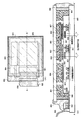
本発明の成膜装置について図1、図2を用いて説明する。図1において、101は搬送室(A)であり、搬送室(A)101には搬送機構(A)102が備えられ、基板103の搬送が行われる。搬送室(A)101は減圧雰囲気にされており、各処理室とはゲートによって遮断されている。各処理室への基板の受け渡しは、ゲートを開けた際に搬送機構(A)102によって行われる。また、搬送室(A)101を減圧するには、油回転ポンプ、メカニカルブースターポンプ、ターボ分子ポンプ若しくはクライオポンプなどの排気ポンプを用いることが可能であるが、水分の除去に効果的なクライオポンプが好ましい。
【0014】
図1の成膜装置では、搬送室(A)101の側面に排気ポート104が設けられ、その下に排気ポンプが設置される。このような構造とすると排気ポンプのメンテナンスが容易になるという利点がある。
【0015】
以下に、各処理室についての説明を行う。なお、搬送室(A)101は減圧雰囲気となるので、搬送室(A)101に直接的に連結された処理室には全て排気ポンプ(図示せず)が備えられている。排気ポンプとしては上述の油回転ポンプ、メカニカルブースターポンプ、ターボ分子ポンプ若しくはクライオポンプが用いられる。
【0016】
まず、105は基板のセッティング(設置)を行うストック室であり、ロードロック室とも呼ばれる。ストック室105はゲート100aにより搬送室(A)101と遮断され、ここに基板103をセットしたキャリア(図示せず)が配置される。なお、ストック室105は基板搬入用と基板搬出用とで部屋が区別されていても良い。また、ストック室105は上述の排気ポンプと高純度の窒素ガスまたは希ガスを導入するためのパージラインを備えている。
【0017】
また、本実施例では基板103を、素子形成面を下向きにしてキャリアにセットする。これは後に気相成膜(スパッタまたは蒸着による成膜)を行う際に、フェイスダウン方式(デポアップ方式ともいう)を行いやすくするためである。フェイスダウン方式とは、基板の素子形成面が下を向いた状態で成膜する方式をいい、この方式によればゴミの付着などを抑えることができる。
【0018】
次に、106は搬送室(B)であり、ストック室105とはゲート100bを介して連結され、搬送機構(B)107を備えている。また、108は焼成室(ベーク室)であり、ゲート100cを介して搬送室(B)106と連結している。なお、焼成室108は基板の面の上下を反転させる機構を有する。即ち、フェイスダウン方式で搬送されてきた基板はここで一旦フェイスアップ方式に切り替わる。これは次の液相成膜室109での処理がフェイスアップ方式で行えるようにするためである。また逆に、液相成膜室109で処理を終えた基板は再び焼成室108に戻ってきて焼成され、再び上下を反転させてフェイスダウン方式に切り替わり、ストック室105へ戻る。
【0019】
ところで液相成膜室109はゲート100dを介して搬送室(B)106と連結している。液相成膜室109はEL材料を含む溶液を基板上に塗布することでEL材料を含む膜を形成する成膜室であり、本発明では液相成膜室109で高分子系(ポリマー系)有機EL材料を成膜する。なお、成膜されるEL材料は、発光層として用いるものだけでなく、電荷注入層または電荷輸送層をも含む。また、公知の如何なる高分子系有機EL材料を用いても良い。
【0020】
発光層となる代表的な有機EL材料としては、PPV(ポリパラフェニレンビニレン)誘導体、PVK(ポリビニルカルバゾール)誘導体またはポリフルオレン誘導体が挙げられる。これはπ共役ポリマーとも呼ばれる。また、電荷注入層としては、PEDOT(ポリチオフェン)またはPAni(ポリアニリン)が挙げられる。
【0021】
ここで液相成膜室109の詳細な説明を、図2を用いて行う。なお、本実施形態では液相成膜室109としてスピンコータ室を用いた例を示す。但し、スピンコータに限定する必要はなく、液相成膜室はディスペンサー、印刷またはインクジェットを用いた成膜室であっても構わない。
【0022】
図2(A)は液相成膜室109を上面から見た図である。201は塗布カップであり、その中心にチャック202が設けられ、搬送されてきた基板203はチャック202に支持される。また、204は塗布ノズルであり、先端部から有機EL材料が吐出される。
【0023】
さらに、本発明では液相成膜室109に酸化セル(酸化室)205が設けられている。本発明では、この酸化セル205内で周期表の1族または2族に属する元素からなる固体(以下、酸化剤という)を酸化(燃焼)させ、液相成膜室109の内部の酸素をゲッタリング(捕獲)する。このとき、ゲート100dを閉めておけば液相成膜室109は密閉空間となるため、効率良く酸素をゲッタリングすることができる。
【0024】
また、図2(B)は液相成膜室109を、図2(A)のA−A’で切断した断面を見た図である。チャック202は回転軸206に連結しており、回転軸206は軸受けとなる制御機構207によって駆動される。また、酸化セル205の下にはヒータ208が設置され、酸化セル205内に設けられた酸化剤209は、ヒータ208によって加熱されて酸化する。なお、酸化セル205自体に電流を流して抵抗加熱により酸化剤209を酸化させても良い。
【0025】
また、酸化セル205の入り口に密閉可能な蓋を設け、その蓋を開閉することで酸化剤209の酸化する時間を調節することもできる。このような方式は室温で自然発火するような元素(代表的にはナトリウム)を用いる場合に有効な手法である。即ち、有機EL材料を成膜する前に所定の時間だけ酸化剤209を酸化させ、蓋を閉めて酸化セル205を密閉して酸素の供給を断つことで酸化を強制的に終了させる。そして、再び基板が搬送されてきたら蓋を開け、酸化剤209を酸化させる。この繰り返しにより複数枚の基板を酸化剤の交換なしで処理することが可能となり、製造スループットを向上させることができる。
【0026】
以上のように、図1に示した成膜装置は液相成膜室109に酸化セル205が備えられており、防塵板210で液相成膜室109を密閉空間とすることができる。そのため、酸化セル205内で周期表の1族または2族に属する元素を酸化させることで容易に成膜雰囲気中の酸素を除去することができる。即ち、酸素濃度が1ppb以下(好ましくは0.1ppb以下)の不活性雰囲気中で有機EL材料を成膜することが可能となる。
【0027】
また、このような不活性雰囲気を与圧(好ましくは2〜3気圧)としておくことで液相成膜室109内の圧力を高め、酸素の混入を極力防ぐ手段をとっても良い。
【0028】
次に、110で示されるのはEL素子の画素電極となる陰極もしくは陽極の表面を処理する処理室(以下、前処理室という)であり、前処理室110はゲート100eにより搬送室(A)101と遮断される。前処理室はEL素子の作製プロセスによって様々に変えることができるが、本実施例では画素電極の表面に紫外光を照射しつつ100〜120℃で加熱できるようにする。このような前処理は、EL素子の陽極表面を処理する際に有効である。
【0029】
次に、111は蒸着法またはスパッタ法により導電膜または有機EL材料を形成するための気相成膜室であり、ゲート100fを介して搬送室(A)101に連結される。本実施形態では気相成膜室111として蒸着室を設けており、内部に複数の蒸着源を設置できる。また、抵抗加熱または電子ビームにより蒸着源を蒸発させ、成膜を行うことができる。
【0030】
この気相成膜室111で形成される導電膜はEL素子の陰極側の電極として設けられる導電膜であり、仕事関数の小さい金属、代表的には周期表の1族もしくは2族に属する元素(代表的にはリチウム、マグネシウム、セシウム、カルシウム、カリウム、バリウム、ナトリウムもしくはベリリウム)またはそれらに近い仕事関数をもつ金属を蒸着できる。また、低抵抗な導電膜としてアルミニウム、銅もしくは銀を蒸着することもできる。さらに、透明導電膜として酸化インジウムと酸化スズとの化合物からなる導電膜や酸化インジウムと酸化亜鉛との化合物からなる導電膜を蒸着法により形成することも可能である。
【0031】
また、気相成膜室111では公知のあらゆるEL材料(特に低分子系有機EL材料)を形成することが可能である。発光層の代表例としてはAlq3(トリス−8−キノリノラトアルミニウム錯体)もしくはDSA(ジスチルアリーレン誘導体)があり、電荷注入層の代表例としてはCuPc(銅フタロシアニン)、LiF(フッ化リチウム)もしくはacacK(カリウムアセチルアセトネート)があり、電荷輸送層の代表例としてはTPD(トリフェニルアミン誘導体)もしくはNPD(アントラセン誘導体)が挙げられる。
【0032】
また、上記EL材料と蛍光物質(代表的には、クマリン6、ルブレン、ナイルレッド、DCM、キナクリドン等)とを共蒸着することも可能である。蛍光物質としては公知の如何なる材料を用いても良い。また、EL材料と周期表の1族または2族に属する元素とを共蒸着して発光層の一部に電荷輸送層または電荷注入層としての役割をもたせることも可能である。なお、共蒸着とは、同時に蒸着源を加熱し、成膜段階で異なる物質を混合する蒸着法をいう。
【0033】
いずれにしてもゲート100fによって搬送室(A)101と遮断され、真空下で有機EL材料または導電膜の成膜が行われる。なお、成膜はフェイスダウン方式(デポアップ方式)で行われる。
【0034】
次に、112は封止室(封入室またはグローブボックスともいう)であり、ゲート100gを介して搬送室(A)101に連結されている。封止室112では、最終的にEL素子を密閉空間に封入するための処理が行われる。この処理は形成されたEL素子を酸素や水分から保護するための処理であり、シーリング材で機械的に封入する、又は熱硬化性樹脂若しくは紫外光硬化性樹脂で封入するといった手段を用いる。
【0035】
シーリング材としては、ガラス、セラミックス、金属などの材料を用いることができるが、シーリング材側に光を出射する場合は透光性でなければならない。また、シーリング材と上記EL素子が形成された基板とは熱硬化性樹脂又は紫外光硬化性樹脂を用いて貼り合わせられ、熱処理又は紫外光照射処理によって樹脂を硬化させて密閉空間を形成する。この密閉空間の中に酸化バリウム等の乾燥剤を設けることも有効である。
【0036】
また、シーリング材とEL素子の形成された基板との空間を熱硬化性樹脂若しくは紫外光硬化性樹脂で充填することも可能である。この場合、熱硬化性樹脂若しくは紫外光硬化性樹脂の中に酸化バリウム等の乾燥剤を添加しておくことは有効である。
【0037】
図1に示した成膜装置では、封止室112の内部に紫外光を照射するための機構(以下、紫外光照射機構という)113が設けられており、この紫外光照射機構113から発した紫外光によって紫外光硬化性樹脂を硬化させる構成となっている。なお、封止室112内の作業は、グローブを用いた手作業であっても構わないが、コンピュータ制御により機械的に行われるような構造となっていることが好ましい。シーリング材を用いる場合には、液晶のセル組み工程で用いられるようなシール剤(ここでは熱硬化性樹脂若しくは紫外光硬化性樹脂)を塗布する機構と、基板を貼り合わせる機構と、シール剤を硬化させる機構とが組み込まれていることが好ましい。
【0038】
また、封止室112の内部は排気ポンプを取り付けることで減圧することも可能である。上記封入工程をロボット操作で機械的に行う場合には、減圧下で行うことで酸素や水分の混入を防ぐことができる。また、逆に封止室112の内部を与圧とすることも可能である。この場合、高純度な窒素ガスや希ガスでパージしつつ与圧とし、外気から酸素等が侵入することを防ぐ。
【0039】
次に、封止室112には受渡室(パスボックス)114が連結される。受渡室114には搬送機構(C)115が設けられ、封止室112でEL素子の封入が完了した基板を受渡室114へと搬送する。受渡室114も排気ポンプを取り付けることで減圧することが可能である。この受渡室114は封止室112を直接外気に晒さないようにするための設備であり、ここから基板を取り出す。
【0040】
以上のように、図1に示した成膜装置を用いることで完全にEL素子を密閉空間に封入するまで外気に晒さずに済む。さらに、液相成膜室109では、酸素濃度が1ppb以下の不活性雰囲気にて有機EL材料の成膜を行うため、殆ど酸素のない状態での成膜が可能となる。以上のことから従来以上に信頼性の高いEL表示装置を作製することが可能となる。
【0041】
【実施例】
〔実施例1〕
本実施例では、図1に示した液相成膜室109とは異なる構造の液相成膜室を設けた例について図3を用いて説明する。図3(A)は液相成膜室301の上面図であり、塗布カップ201、チャック202、基板203及び塗布ノズル204は図2と同様である。図3に示した成膜装置の特徴は、図2の酸化セル205の代わりに酸化炉302を成膜装置の外部に設け、配管303により液相成膜室301と酸化炉302とを連結している点にある。
【0042】
即ち、図3(B)に示すように防塵フード310の一部に配管303の一方の口(吸気口)が取り付けられ、配管303のもう一方の口(排気口)が酸化炉302に取り付けられている。
【0043】
また、図3(C)に示すように酸化炉302は酸化セル304、ヒータ305を有し、酸化セル304の内部には周期表の1族または2族に属する元素からなる酸化剤306が設置される。また、本実施例では酸化セル304への酸素の供給を遮断するシャッタ307も設けられている。
【0044】
本実施例では、酸化炉302の内部で酸化剤306が酸化(燃焼)する。そのとき、消費された酸素は配管303を通じて液相成膜室301から供給され、その結果、液相成膜室301の内部の酸素濃度が減少する。図1の成膜装置と根本的に異なる点は、成膜装置の近くに熱源を備えなくて済む点が挙げられる。液相成膜室301で成膜される高分子系有機EL材料は有機溶媒に溶かして塗布されるため、熱源が遠い方が管理は容易である。
【0045】
なお、本実施例の液相成膜室301は図1に示した成膜装置の成膜室の一つとして用いることが可能である。
【0046】
〔実施例2〕
本実施例では、図1の成膜装置において液相成膜室として赤色、緑色及び青色の発光層をストライプ状に形成する液相成膜室を設けた例を示す。本実施例の液相成膜室について図4を用いて説明する。
【0047】
図4(A)は本実施例の液相成膜室400を側面からみた外観図であり、図4(B)は前面からみた外観図である。図4(A)において、401は支持台、402は搬送ステージであり、その上に基板403が固定される。搬送ステージ402はX方向(横方向)またはY方向(縦方向)に移動が可能である。
【0048】
支持台401には支持柱404、ホルダー405が取り付けられ、搬送ステージ402の上方に塗布ユニット406が設置される。塗布ユニット406は有機EL材料を含む溶液を基板上に塗布するための機構を備えた装置であり、ヘッド部407に圧縮ガス(加圧された不活性ガス)を送ったり、有機EL材料を含む溶液を供給する装置である。このとき、塗布ユニット406にはサックバック機構(サックバックバルブまたはエアオペレーションバルブを備えた機構)を設けることが好ましい。サックバック機構とは、ダイヤフラムゲージ等を用いた容積変化を利用して配管内の圧力を下げることにより、配管等のノズル口に溜まった液滴をノズル内に引き込むための機構である。
【0049】
また、上記塗布ユニット等は支持台401に取り付けられた防塵フード408に覆われている。防塵フード408には基板を搬送するための入り口が設けられているが、その部分にはゲートが設けられ、支持台401と防塵フード408とで密閉空間が形成される。
【0050】
そして、支持台401には酸化セル409、ヒータ410及び酸化剤411が設けられ、有機EL材料を成膜する前に酸化剤411の酸化が行われる。
【0051】
また、図4の液相成膜室400ではヘッド部407が固定され、基板403を載せた搬送ステージ402がX方向またはY方向へと移動する。即ち、搬送ステージが移動することにより相対的にヘッド部407が基板403上を移動するような機構となっている。勿論、ヘッド部407の方を移動させるような機構とすることも可能であるが、基板側を移動させた方が安定性は良い。
【0052】
以上の構成の液相成膜室400は、有機EL材料(厳密には有機EL材料を溶媒に溶かした混合物)の供給口となるノズルを備えたヘッド部407が基板403上を移動することにより、基板の必要箇所へ有機EL材料を塗布していく。ここでヘッド部407により有機EL材料を塗布していく過程を以下に説明する。
【0053】
図5(A)に示したのは、本発明を実施してπ共役系ポリマーでなる有機EL材料を成膜する様子を模式的に示す図である。図5(A)において、510は基板であり、基板510上には画素部511、ソース側駆動回路512、ゲート側駆動回路513がTFTにより形成されている。ソース側駆動回路512に接続された複数のソース配線とゲート側駆動回路513に接続された複数のゲート配線とで囲まれた領域が画素であり、画素内にはTFTと該TFTに電気的に接続されたEL素子が形成される。画素部511はこのような画素がマトリクス状の配列されて形成されている。
【0054】
ここで514aは電圧を加えることで赤色に発光する有機EL材料(以下、有機EL材料(R)という)と溶媒との混合物(以下、塗布液(R)という)、514bは電圧を加えることで緑色に発光する有機EL材料(以下、有機EL材料(G)という)と溶媒との混合物(以下、塗布液(G)という)、514cは電圧を加えることで青色に発光する有機EL材料(以下、有機EL材料(B)という)と溶媒との混合物(以下、塗布液(B)という)である。
【0055】
なお、これらの有機EL材料はポリマー重合したものを直接溶媒に溶かして塗布する方法と、モノマーを溶媒に溶かしたものを成膜した後に加熱重合させてポリマーとする方法とがあるが、本発明はどちらでも構わない。ここではポリマーとなった有機EL材料を溶媒に溶かして塗布した例を示す。
【0056】
本発明の場合、図4に示したヘッド部407からは塗布液(R)514a、塗布液(G)514b、塗布液(B)514cが別々に塗布され、矢印の方向に向かって塗布される。即ち、赤色に発光すべき画素列、緑色に発光すべき画素列及び青色に発光すべき画素列に、同時にストライプ状の発光層(厳密には発光層の前駆体)が形成される。
【0057】
なお、ここでいう画素列とはバンク521に仕切られた画素の列を指し、バンク521はソース配線の上方に形成されている。即ち、ソース配線に沿って複数の画素が直列に並んだ列を画素列と呼んでいる。但し、ここではバンク521がソース配線の上方に形成された場合を説明したが、ゲート配線の上方に設けられていても良い。この場合は、ゲート配線に沿って複数の画素が直列に並んだ列を画素列と呼ぶ。
【0058】
従って、画素部511は、複数のソース配線もしくは複数のゲート配線の上方に設けられたストライプ状のバンクにより分割された複数の画素列の集合体として見ることができる。そのようにして見た場合、画素部511は、赤色に発光するストライプ状の発光層が形成された画素列、緑色に発光するストライプ状の発光層が形成された画素列及び青色に発光するストライプ状の発光層が形成された画素列からなるとも言える。
【0059】
また、上記ストライプ状のバンクは、複数のソース配線もしくは複数のゲート配線の上方に設けられているため、実質的に画素部511は、複数のソース配線もしくは複数のゲート配線により分割された複数の画素列の集合体と見ることもできる。
【0060】
次に、図5(A)に示したヘッド部(塗布部と言っても良い)407の様子を拡大して図5(B)に示す。
【0061】
ヘッド部407には赤色用ノズル516a、緑色用ノズル516b、青色用ノズル516cが取り付けられている。また各々のノズルの内部には塗布液(R)514a、塗布液(G)514b、塗布液(B)514cが蓄えられている。これらの塗布液は、配管517内に充填された圧縮ガスにより加圧されて画素部511上に押し出される。このようなヘッド部407が紙面に垂直な方向に沿って手前方向に移動することで図5(A)に示したような塗布工程が行われる。
【0062】
ここで518で示される塗布部付近の拡大図を図5(C)に示す。基板510上に設けられた画素部511は、複数のTFT519a〜519cと画素電極520a〜520cとでなる複数の画素の集合体である。図5(B)のノズル516a〜516cに圧縮ガスにより圧力がかかると、その圧力により塗布液514a〜514cが押し出される。
【0063】
なお、画素間には樹脂材料で形成されたバンク521が設けられており、隣接する画素間で塗布液が混合されてしまうことを防いでいる。この構造ではバンク521の幅(フォトリソグラフィの解像度で決まる)を狭くすることで画素部の集積度が向上し、高精細な画像を得ることができる。特に塗布液の粘性が1〜30cpの場合に有効である。
【0064】
但し、塗布液の粘性が30cp以上またはゾル状もしくはゲル状であればバンクを用いないことも可能である。即ち、塗布後の塗布液と塗布面との接触角が十分に大きければ必要以上に塗布液が広がることもないので、バンクで堰き止めておく必要もなくなる。その場合は、最終的に発光層が長円形状(長径と短径の比が2以上の細長い楕円形状)、典型的には画素部の一端から他端にまで及ぶ細長い楕円状で形成されることになる。
【0065】
また、バンク521を形成しうる樹脂材料としてはアクリル、ポリイミド、ポリアミド、ポリイミドアミドを用いることができる。この樹脂材料に予めカーボンや黒色顔料等を設けて樹脂材料を黒色化しておくと、バンク521を画素間の遮光膜として用いることも可能となる。
【0066】
また、ノズル516a、516bまたは516cのいずれかの先端付近に光反射を用いたセンサーを取り付ければ、塗布面とノズルとの距離を常に一定に保つように調節することも可能である。さらに、画素ピッチ(画素間の距離)に応じてノズル516a〜516cの間隔を調節する機構を備えることで、どのような画素ピッチのEL表示装置にも対応することが可能である。
【0067】
こうしてノズル516a〜516cから塗布された塗布液514a〜514cは各々画素電極520a〜520cを覆うようにして塗布される。なお、以上のようなヘッド部407の動作は電気的な信号により制御される。
【0068】
塗布液514a〜514cを塗布したら真空中で加熱処理(ベーク処理または焼成処理)することにより塗布液514a〜514cに含まれる有機溶媒を揮発させ、有機EL材料でなる発光層を形成する。このため、有機溶媒は有機EL材料のガラス転移温度(Tg)よりも低い温度で揮発するものを用いる。また、有機EL材料の粘度により最終的に形成される発光層の膜厚が決まる。この場合、有機溶媒の選定または添加物により粘度を調節することができるが、粘度は1〜50cp(好ましくは5〜20cp)とするのが好ましい。
【0069】
以上のような液相成膜室を用いることにより、赤、緑、青の各色に発光する三種類の発光層を同時に形成することができるため、高いスループットでポリマー系有機EL材料でなる発光層を形成することができる。さらに、インクジェット方式と異なり、一つの画素列では切れ間なくストライプ状に塗布していくことができるため、非常にスループットが高い。
【0070】
また、本実施例の液相成膜室を用いる場合においても、本発明により酸素をゲッタリングしておくことで信頼性の高いEL素子を形成することができる。なお、本実施例の液相成膜室は実施例1に示した液相成膜室(スピンコータ室)と併用して用いることも可能である。
【0071】
〔実施例3〕
本実施例では、実施例2の図5に示した液相成膜室のヘッド部の構造を異なるものとした液相成膜室について説明する。なお、図5と同一の符号を用いている部分に関する記載は実施例2を参照すれば良い。
【0072】
図6(A)は本実施例の液相成膜室のヘッド部を示している。ノズル601a〜601cの内部には、各々ノズルと同軸のロッド602a〜602cが設けられている。さらに、ノズル601a〜601cの内部には、塗布液(R)603a、塗布液(G)603b、塗布液(B)603cが蓄えられている。このロッド602a〜602cを設けることにより、塗布液の固化によるノズルの目詰まりを抑制することができる。
【0073】
このとき、ノズル601a〜601cの内壁は塗布液に対して疎水性とし、ロッド602a〜602cの表面は塗布液に対して親水性とすると良い。ノズル601a〜601cの内壁を疎水性とするには形成材料として疎水性を示す材料を用いれば良く、代表的にはテフロン、PVDF(ポリビニリデンフロライド)または金属(代表的にはステンレス、アルミニウム、ジルコニウム)とすれば良い。また、ロッド602a〜602cの表面を親水性とするには形成材料として親水性を示す材料を用いれば良く、代表的にはナイロンまたはPVA(ポリビニルアルコール)とすれば良い。
【0074】
また、ノズル601a〜601cを金属で形成し、ノズル601a〜601cに超音波をかけることで、塗布液(R)603a、塗布液(G)603b、塗布液(B)603cの固化を抑制することも可能である。
【0075】
ところで、塗布液(R)603a、塗布液(G)603b、塗布液(B)603cの塗布はロッド602a〜602cが被成膜面(本実施例では画素電極520a〜520cの表面)に接した状態で行われる。ロッド602a〜602cは非常に柔らかい材料で形成され、被成膜面をなぞるように移動する。この様子を図6(B)に示す。
【0076】
矢印の方向はノズル601aの移動方向であり、ロッド602aは画素電極520aに接している。即ち、塗布液(R)603aはロッド602aを伝って画素電極520aの表面に塗布される。従って、インクジェット法のように塗布液を飛ばす必要がなく、塗布時の位置ずれといった問題を生じない。
【0077】
以上のように、本実施例のヘッド部を設けた液相成膜室はノズルの目詰まりといった問題を解消しつつ、細かいパターンにも対応して有機EL材料を成膜することが可能である。また、本発明と組み合わせることで、信頼性の高いEL素子を形成することができる。
【0078】
なお、本実施例の構成は実施例2に示した液相成膜室のヘッド部として用いることが可能であり、図1の液相成膜室として用いることが可能である。また、実施例1の液相成膜室と併用しても構わない。
【0079】
〔実施例4〕
本実施例では、実施例3に示したノズルの構造をとは異なる構造のノズルを有した液相成膜室について説明する。なお、図7(A)は塗布前後の待機状態を示しており、図7(B)は塗布時の状態を示している。また、図7(C)、(D)はノズルの断面を上から見た図を示している。
【0080】
図7(A)において、701はノズル、702はロッド、703は塗布液である。各々の材料は実施例2、実施例3を参照すれば良い。また、ノズル701の内壁を塗布液に対して疎水性にし、ロッド702を親水性にしても良い。
【0081】
本実施例のノズル701は内壁にロッドストッパ部704a、704bを有し、ロッドストッパ部704aは中央に塗布液を通すための孔が設けられている。また、ロッド702はストッパ部705を有し、ストッパ部705の直径はロッドストッパ部704aに設けられた孔の直径よりも大きい。
【0082】
即ち、図7(A)に示すようにストッパ部705はロッドストッパ部704に引っかかるようになっており、塗布前後の待機状態では塗布液703の移動経路が封じられるような仕組みになっている。その結果、待機状態では塗布液703がノズルの先端から流出しない。
【0083】
また、図7(B)に示すように、塗布液を塗布する際はロッド702の先端部706が被成膜面707に接し、ロッド702がノズル701の内部に押し込まれる。そして、ストッパ部705がロッドストッパ部704bに接した状態でロッド702が止まる。この状態で、塗布液703はロッド702を伝ってノズルから流出し、被成膜面707に塗布される。
【0084】
このとき、ロッドの先端部706は球状としておくことが望ましい。こうすることで被成膜面707を傷つけることを防ぐことができる。
【0085】
以上の構造のノズルを有した本実施例の液相成膜室は、実施例2で説明したサックバック機構を設けなくても塗布液の流出を防ぐことができる。また、本発明と組み合わせることで、信頼性の高いEL素子を形成することができる。なお、本実施例の構成は実施例2に示した液相成膜室のヘッド部として用いることが可能であり、図1の液相成膜室として用いることが可能である。また、実施例1の液相成膜室と併用しても構わない。
【0086】
〔実施例5〕
本実施例では、図1の成膜装置において前処理室110にプラズマ処理を行う機構を備える例を示す。EL素子の陰極表面に前処理を行う場合、金属からなる陰極表面の自然酸化物を除去することが望ましい。本実施例では、フッ素または塩素を含むガスを用いて陰極表面にプラズマ処理を行い、自然酸化物を除去する機構を有する。
【0087】
なお、本実施例の構成は、実施例1〜実施例3に示したいずれの構成とも自由に組み合わせて実施することが可能である。
【0088】
〔実施例6〕
本実施例では、図1の成膜装置において前処理室110にスパッタ処理を行う機構を備える例を示す。EL素子の陰極表面に前処理を行う場合、金属からなる陰極表面の自然酸化物を除去することが望ましい。本実施例では、希ガスや窒素等の不活性ガスを用いて陰極表面に対してスパッタ処理を行い、自然酸化物を除去する機構を有する。
【0089】
なお、本実施例の構成は、実施例1〜実施例3に示したいずれの構成とも自由に組み合わせて実施することが可能である。
【0090】
〔実施例7〕
本実施例では、図1に示した成膜装置を用いて発光装置(具体的にはEL表示装置)を作製する例を示す。
【0091】
まず、基板上に公知の技術によりTFTを作製し、画素部及び駆動回路部とを形成する。本実施例では本出願人による特開平5−107561号公報に記載の技術を用いて同一基板上に画素部及び駆動回路部を形成する。なお、画素部に設けられる画素TFTには透明導電膜からなる画素電極が電気的に接続され、この画素電極がEL素子の陽極となる。
【0092】
TFT及び画素電極の形成までを終えた基板(以下、アクティブマトリクス基板という)が完成したら、そのアクティブマトリクス基板を図1のストック室105に設置する。
【0093】
次に、前処理室110へアクティブマトリクス基板を搬送し、画素電極の表面に対して前処理を行う。本実施例では、オゾン雰囲気において紫外光を照射することで画素電極の表面状態を改善する。
【0094】
次に、気相成膜室111にアクティブマトリクス基板を搬送し、正孔注入層として銅フタロシアニン膜を蒸着法により形成する。本実施例では、膜厚を20nmとするが特に限定はない。
【0095】
次に一旦アクティブマトリクス基板をストック室105に戻し、そのアクティブマトリクス基板を搬送機構(B)107により焼成室108へと搬送する。このとき、焼成室ではアクティブマトリクス基板を反転させ、TFTを形成した面が上を向くようにする。
【0096】
次に、反転させたアクティブマトリクス基板を図2に示される構造の液相成膜室109へ搬送する。なお、液相成膜室109は実施例1〜4のいずれの構造を有していても良い。そして、まず酸化セル205内にて酸化剤(本実施例ではマグネシウム)を酸化させ、液相成膜室109の内部の酸素濃度を1ppb以下にまで低減する。その後、スピンコート法によりジクロロメタンに溶解させたポリフェニレンビニレンの前駆体を塗布する。
【0097】
次に、上記前駆体を塗布したアクティブマトリクス基板を焼成室108へ搬送し、ポリフェニレンビニレンの前駆体を焼成する。こうして前駆体が重合してポリマー化し、ポリフェニレンビニレン膜からなる発光層が形成される。焼成処理が終了したら再度アクティブマトリクス基板を反転させてストック室105へ戻す。
【0098】
次に、アクティブマトリクス基板を気相成膜室111に搬送し、膜厚400nmのアルミニウム膜を蒸着する。このアルミニウム膜がEL素子の陰極として機能する。なお、本実施例で用いるアルミニウム膜はチタン、スカンジウムもしくはシリコンを含むアルミニウム合金膜であっても良い。また、アルミニウム膜の代わりに銅もしくは銅合金または銀からなる導電膜を形成しても良い。
【0099】
次に、アクティブマトリクス基板を不活性ガス(窒素ガスまたは希ガス)で充填された封止室112へ搬送する。ここではアクティブマトリクス基板上にシール材を形成し、EL素子が形成された面を覆うようにカバー材を貼り合わせる。そのため、EL素子が不活性ガスの充填された密閉空間に封入され、完全に外気と遮断される。なお、密閉空間に吸湿性物質(好ましくは酸化バリウム)を設けることは有効である。また、不活性ガスの代わりに樹脂を充填することも可能である。その場合も、樹脂中に吸湿性物質を設けることは有効である。
【0100】
こうしてアクティブマトリクス基板及びカバー材をシール材により張り合わせたら、紫外光照射機構113を用いてシール材に紫外光を照射し硬化させる。以上のようにしてEL素子の封入処理が終了したら、受渡室114へ封入後のアクティブマトリクス基板を搬送する。
【0101】
以上のように、本発明の成膜装置を用いることで極力酸素を排除した環境でEL素子が形成され、完全に外気と遮断された状態となるまでのプロセスを一貫して行うことが可能である。
【0102】
なお、本実施例ではアクティブマトリクス型EL表示装置の作製工程の例を示しているが、本実施例はパッシブマトリクス型EL表示装置の作製工程に対しても実施できる。また、本実施例はバックライト等に用いられる発光装置の作製工程に対しても実施できる。
【0103】
〔実施例8〕
本実施例では、図1に示した成膜装置を用いて実施例7とは異なる構造の発光装置を作製する例を示す。なお、本実施例ではアクティブマトリクス型EL表示装置を例にとって説明する。
【0104】
まず、基板上に特開平5−107561号公報に記載の技術を用いて画素部及び駆動回路部を形成する。なお、本実施例では画素電極としてアルミニウムもしくはアルミニウム合金からなる導電膜を用いる。即ち、本実施例では画素電極がEL素子の陰極となる。
【0105】
アクティブマトリクス基板が完成したら、そのアクティブマトリクス基板を図1のストック室105に設置する。
【0106】
次に、前処理室110へアクティブマトリクス基板を搬送し、画素電極の表面に対して前処理を行う。本実施例では、フッ素または塩素を含むガスを用いて画素電極の表面に対してプラズマ処理を行い、自然酸化物を除去する。
【0107】
次に、気相成膜室111にアクティブマトリクス基板を搬送し、電子注入層としてフッ化リチウム膜を蒸着法により形成する。本実施例では、膜厚を20nmとするが特に限定はない。
【0108】
次に一旦アクティブマトリクス基板をストック室105に戻し、そのアクティブマトリクス基板を搬送機構(B)107により焼成室108へと搬送する。次いでアクティブマトリクス基板を反転させる。
【0109】
次に、反転させたアクティブマトリクス基板を図4に示される構造の液相成膜室109へ搬送する。そして、まず酸化セル409内にて酸化剤(本実施例ではナトリウム)を酸化させ、液相成膜室109の内部の酸素濃度を1ppb以下にまで低減する。その後、図5に示した塗布法によりトルエンに溶解させたポリビニルカルバゾールの前駆体を塗布する。
【0110】
次に、上記前駆体を塗布したアクティブマトリクス基板を焼成室108へ搬送し、ポリビニルカルバゾールの前駆体を焼成する。こうして前駆体が重合してポリマー化し、ポリビニルカルバゾール膜からなる発光層が形成される。焼成処理が終了したら再度アクティブマトリクス基板を反転させてストック室105へ戻す。
【0111】
次に、アクティブマトリクス基板を気相成膜室111に搬送し、膜厚20nmの銅フタロシアニン膜を蒸着し、さらに膜厚200nm透明導電膜(具体的には酸化インジウムと酸化亜鉛との化合物膜)を蒸着する。この透明導電膜がEL素子の陽極として機能する。なお、本実施例で用いる透明導電膜は酸化インジウムと酸化スズとの化合物膜であっても良い。
【0112】
次に、アクティブマトリクス基板を不活性ガス(窒素ガスまたは希ガス)で充填された封止室112へ搬送する。ここではアクティブマトリクス基板上にシール材を形成し、EL素子が形成された面を覆うようにカバー材を貼り合わせる。そのため、EL素子が不活性ガスの充填された密閉空間に封入され、完全に外気と遮断される。なお、密閉空間に吸湿性物質(好ましくは酸化バリウム)を設けることは有効である。また、不活性ガスの代わりに樹脂を充填することも可能である。その場合も、樹脂中に吸湿性物質を設けることは有効である。
【0113】
こうしてアクティブマトリクス基板及びカバー材をシール材により張り合わせたら、紫外光照射機構113を用いてシール材に紫外光を照射し硬化させる。以上のようにしてEL素子の封入処理が終了したら、受渡室114へ封入後のアクティブマトリクス基板を搬送する。
【0114】
以上のように、本発明の成膜装置を用いることで極力酸素を排除した環境でEL素子が形成され、完全に外気と遮断された状態となるまでのプロセスを一貫して行うことが可能である。
【0115】
〔実施例9〕
本実施例では、本発明を用いて作製したアクティブマトリクス型EL表示装置について図8(A)、(B)を用いて説明する。図8(A)は、EL素子の形成されたアクティブマトリクス基板において、EL素子の封入まで行った状態を示す上面図である。点線で示された801はソース側駆動回路、802はゲート側駆動回路、803は画素部である。また、804はカバー材、805は第1シール材、806は第2シール材であり、第1シール材805で囲まれた内側のカバー材とアクティブマトリクス基板との間には充填材807(図8(B)参照)が設けられる。
【0116】
なお、808はソース側駆動回路801、ゲート側駆動回路802及び画素部803に入力される信号を伝達するための接続配線であり、外部機器との接続端子となるFPC(フレキシブルプリントサーキット)809からビデオ信号やクロック信号を受け取る。
【0117】
ここで、図8(A)をA−A’で切断した断面に相当する断面図を図8(B)に示す。なお、図8(A)、(B)では同一の部位に同一の符号を用いている。
【0118】
図8(B)に示すように、基板800上には画素部803、ソース側駆動回路801が形成されており、画素部803はEL素子に流れる電流を制御するためのTFT(以下、電流制御用TFTという)851とそのドレインに電気的に接続された画素電極852を含む複数の画素により形成される。本実施例では電流制御用TFT851をpチャネル型TFTとする。また、ソース側駆動回路801はnチャネル型TFT853とpチャネル型TFT854とを相補的に組み合わせたCMOS回路を用いて形成される。
【0119】
各画素は画素電極の下にカラーフィルタ(R)855、カラーフィルタ(G)856及びカラーフィルタ(B)(図示せず)を有している。ここでカラーフィルタ(R)とは赤色光を抽出するカラーフィルタであり、カラーフィルタ(G)は緑色光を抽出するカラーフィルタ、カラーフィルタ(B)は青色光を抽出するカラーフィルタである。なお、カラーフィルタ(R)855は赤色発光の画素に、カラーフィルタ(G)856は緑色発光の画素に、カラーフィルタ(B)は青色発光の画素に設けられる。
【0120】
これらのカラーフィルタを設けた場合の効果としては、まず発光色の色純度が向上する点が挙げられる。例えば赤色発光の画素からはEL素子から赤色光が放射される(本実施例では画素電極側に向かって放射される)が、この赤色光を、赤色光を抽出するカラーフィルタに通すことにより赤色の純度を向上させることができる。このことは、他の緑色光、青色光の場合においても同様である。
【0121】
また、従来のカラーフィルタを用いない構造ではEL表示装置の外部から侵入した可視光がEL素子の発光層を励起させてしまい、所望の発色が得られない問題が起こりうる。しかしながら、本実施例のようにカラーフィルタを設けることでEL素子には特定の波長の光しか入らないようになる。即ち、外部からの光によりEL素子が励起されてしまうような不具合を防ぐことが可能である。
【0122】
なお、カラーフィルタを設ける構造は従来提案されているが、EL素子は白色発光のものを用いていた。この場合、赤色光を抽出するには他の波長の光をカットしていたため、輝度の低下を招いていた。しかしながら、本実施例では、例えばEL素子から発した赤色光を、赤色光を抽出するカラーフィルタに通すため、輝度の低下を招くようなことがない。
【0123】
次に、画素電極852は透明導電膜で形成され、EL素子の陽極として機能する。また、画素電極852の両端には絶縁膜857が形成され、さらに赤色に発光する発光層858、緑色に発光する発光層859が形成される。なお、図示しないが隣接する画素には青色に発光する発光層を設けられ、赤、緑及び青に対応した画素によりカラー表示が行われる。勿論、青色の発光層が設けられた画素は青色を抽出するカラーフィルタが設けられている。
【0124】
なお、発光層858、859の成膜方法は図1に示した成膜装置を用いて行われる。また、実際に発光層を成膜する液相成膜室は実施例1〜4のいずれの構成を有する液相成膜室であっても良い。また、材料として有機材料だけでなく無機材料を用いることができる。また、発光層だけでなく電子注入層、電子輸送層、正孔輸送層または正孔注入層を組み合わせた積層構造としても良い。
【0125】
また、各発光層の上にはEL素子の陰極860が遮光性を有する導電膜でもって形成される。この陰極860は全ての画素に共通であり、接続配線808を経由してFPC809に電気的に接続されている。
【0126】
次に、第1シール材805をディスペンサー等で形成し、スペーサ(図示せず)を撒布してカバー材804を貼り合わせる。そして、アクティブマトリクス基板、カバー材804及び第1シール材805で囲まれた領域内に充填材807を真空注入法により充填する。
【0127】
また、本実施例では充填材807に予め吸湿性物質861として酸化バリウムを添加しておく。なお、本実施例では吸湿性物質を充填材に添加して用いるが、塊状に分散させて充填材中に封入することもできる。また、図示されていないがスペーサの材料として吸湿性物質を用いることも可能である。
【0128】
次に、充填材807を紫外線照射または加熱により硬化させた後、第1シール材805に形成された開口部(図示せず)を塞ぐ。第1シール材805の開口部を塞いだら、導電性材料862を用いて接続配線808及びFPC809を電気的に接続させる。さらに、第1シール材805の露呈部及びFPC809の一部を覆うように第2シール材806を設ける。第2シール材806は第1シール材807と同様の材料を用いれば良い。
【0129】
以上のような方式を用いてEL素子を充填材807に封入することにより、EL素子を外部から完全に遮断することができ、外部から水分や酸素等の有機材料の酸化を促す物質が侵入することを防ぐことができる。従って、信頼性の高いEL表示装置を作製することができる。
【0130】
また、本発明を用いることで既存の液晶表示装置用の製造ラインを転用させることができるため、整備投資の費用が大幅に削減可能であり、歩留まりの高いプロセスで1枚の基板から複数の発光装置を生産することができるため、大幅に製造コストを低減しうる。
【0131】
なお、本実施例のEL表示装置は実施例1〜7のいずれの構成を組み合わせた成膜装置を用いても作製することができる。
【0132】
〔実施例10〕
本実施例では、実施例9に示したEL表示装置において、EL素子から発する光の放射方向とカラーフィルタの配置を異ならせた場合の例について示す。説明には図9を用いるが、基本的な構造は図8(B)と同様であるので変更部分に新しい符号を付して説明する。
【0133】
本実施例では画素部901には電流制御用TFT902としてnチャネル型TFTが用いられている。また、電流制御用TFT902のドレインには画素電極903が電気的に接続され、この画素電極903は遮光性を有する導電膜で形成されている。本実施例では画素電極903がEL素子の陰極となる。
【0134】
また、本発明を用いて形成された赤色に発光する発光層858、緑色に発光する発光層859の上には各画素に共通な透明導電膜904が形成される。この透明導電膜904はEL素子の陽極となる。
【0135】
さらに、本実施例ではカラーフィルタ(R)905、カラーフィルタ(G)906及びカラーフィルタ(B)(図示せず)がカバー材804に形成されている点に特徴がある。本実施例のEL素子の構造とした場合、発光層から発した光の放射方向がカバー材側に向かうため、図9の構造とすればその光の経路にカラーフィルタを設置することができる。
【0136】
本実施例のようにカラーフィルタ(R)905、カラーフィルタ(G)906及びカラーフィルタ(B)(図示せず)をカバー材804に設けると、アクティブマトリクス基板の工程を少なくすることができ、歩留まり及びスループットの向上を図ることができるという利点がある。
【0137】
なお、本実施例のEL表示装置は実施例1〜8のいずれの構成を組み合わせた成膜装置を用いても作製することができる。
【0138】
【発明の効果】
本発明の成膜装置を用いることで、EL材料からなる発光層の劣化を最小限に抑制することができ、EL素子の信頼性を高めることができる。従って、EL素子を用いた発光装置の信頼性を大幅に向上させることが可能となる。
【図面の簡単な説明】
【図1】 成膜装置の構造を示す図。
【図2】 液相成膜室の構造を示す図。
【図3】 液相成膜室の構造を示す図。
【図4】 液相成膜室の構造を示す図。
【図5】 液相成膜室に備えられたヘッド部の構成を示す図。
【図6】 液相成膜室に備えられたヘッド部の構成を示す図。
【図7】 液相成膜室に備えられたヘッド部の構成を示す図。
【図8】 EL表示装置の断面構造を示す図。
【図9】 EL表示装置の断面構造を示す図。[0001]
BACKGROUND OF THE INVENTION
The present invention relates to an anode, a cathode, and a luminescent material from which EL (Electro Luminescence) is obtained, and in particular, a thin film used for manufacturing an EL element having a structure in which a luminescent organic material (hereinafter referred to as an organic EL material) is sandwiched. The present invention relates to a forming apparatus and a method for manufacturing a light-emitting device using the forming apparatus.
[0002]
[Prior art]
In recent years, a display device (EL display device) using an EL element as a self-luminous element using an EL phenomenon of an organic EL material has been developed. Since the EL display device is a self-luminous type, it does not require a backlight like a liquid crystal display device, and further has a wide viewing angle, and thus is promising as a display unit of a portable device used outdoors.
[0003]
There are two types of EL display devices, a passive type (simple matrix type) and an active type (active matrix type), both of which are actively developed. In particular, active matrix EL display devices are currently attracting attention. In addition, EL materials used as a light emitting layer of an EL element include an organic material and an inorganic material, and the organic material is further classified into a low molecular (monomer) organic EL material and a high molecular (polymer) organic EL material. . Both have been actively studied, but attention has been focused on polymer-based organic EL materials that are easier to handle and have higher heat resistance than low-molecular-weight organic EL materials.
[0004]
However, when an organic EL material is oxidized, the molecular structure is easily changed and the light emitting ability is lost. That is, when the light emitting layer made of the organic EL material is oxidized, the EL element loses its light emitting ability and deteriorates. Therefore, after forming an organic EL material, it is necessary to eliminate oxygen (O 2 ) that promotes oxidation of the organic EL material as much as possible in order to form a highly reliable EL element.
[0005]
In the case of a low molecular weight organic EL material, film formation is performed by a vapor deposition method under vacuum, so that mixing of oxygen into the element hardly causes a problem. In addition, after the organic EL material is formed, it is sealed in a sealed space without being released to the atmosphere, so that the EL element can be completed without being exposed to the outside air (atmosphere) consistently from the film forming process.
[0006]
However, in the case of a high molecular weight organic EL material, it is difficult to form a film in a vacuum, and therefore, an ink jet method, a spin coating method, or a printing method is performed in an inert gas such as nitrogen or a rare gas. In addition, the polymer organic EL material is particularly vulnerable to oxygen, and is easily oxidized and deteriorated by the presence of slight oxygen. Although it is possible to suppress the deterioration to a level with no problem by setting the oxygen concentration in the inert gas to 1 ppm or less, there is a problem in securing long-term reliability.
[0007]
[Problems to be solved by the invention]
This invention is made | formed in view of the said problem, and makes it a subject to provide the method for further improving the reliability of the light-emitting device using a luminescent raw material. It is another object of the present invention to provide a film formation apparatus for forming such a highly reliable light-emitting device.
[0008]
[Means for Solving the Problems]
In the present invention, before forming an EL material (especially an organic EL material), an element (alkali metal element or alkaline earth metal element) belonging to Group 1 or Group 2 of the periodic table is oxidized inside the film formation chamber. The oxygen inside the film formation chamber is removed. That is, oxygen is chemically removed (gettering) using the property of alkali metal elements or alkaline earth metal elements that are very easily oxidized.
[0009]
Specifically, an element belonging to Group 1 or Group 2 of the periodic table is installed in an oxidation cell provided in the film forming chamber, and the element belonging to Group 1 or Group 2 of the periodic table in the oxidation cell. Oxidize. At this time, when an element that does not oxidize at room temperature is used, the oxidation cell may be heated. In the case of using an element that oxidizes at room temperature, it is stored in an alcohol, sealed in an oxidation cell while the supply of oxygen is cut off, and carried into a film formation chamber for oxidation.
[0010]
When the present invention is implemented, oxygen present in the film forming chamber is oxidized with an element belonging to Group 1 or 2 of the periodic table while an element belonging to Group 1 or 2 of the periodic table is oxidized. Is consumed by. That is, it may be considered that an element belonging to Group 1 or Group 2 of the periodic table getters oxygen.
[0011]
The present invention is particularly effective as a pretreatment when a high molecular organic EL material is formed by a liquid phase method (inkjet method, spin coating method, printing method or dispensing method). It is also possible to perform the pretreatment when forming the organic EL material by a vapor phase method (evaporation method or sputtering method).
[0012]
As described above, as a pretreatment for forming an EL material, an oxidation reaction between an element belonging to Group 1 or Group 2 of the periodic table and oxygen is used in the deposition chamber. As a result, the oxygen concentration in the deposition chamber can be reduced to 1 ppb or less (preferably 0.1 ppb or less). As a result, the EL material can be deposited in an inert atmosphere having an oxygen concentration of 1 ppb or less (preferably 0.1 ppb or less). That is, an EL element can be formed in a state close to oxygen-free, and an EL display device with higher reliability than before can be obtained.
[0013]
DETAILED DESCRIPTION OF THE INVENTION
A film forming apparatus of the present invention will be described with reference to FIGS. In FIG. 1,
[0014]
In the film forming apparatus of FIG. 1, an exhaust port 104 is provided on the side surface of the transfer chamber (A) 101, and an exhaust pump is installed therebelow. Such a structure has an advantage that maintenance of the exhaust pump is facilitated.
[0015]
Hereinafter, each processing chamber will be described. Since the transfer chamber (A) 101 is in a reduced pressure atmosphere, all the processing chambers directly connected to the transfer chamber (A) 101 are provided with an exhaust pump (not shown). As the exhaust pump, the above-described oil rotary pump, mechanical booster pump, turbo molecular pump, or cryopump is used.
[0016]
First, reference numeral 105 denotes a stock chamber for setting (installing) a substrate, which is also called a load lock chamber. The stock chamber 105 is cut off from the transfer chamber (A) 101 by the
[0017]
In this embodiment, the substrate 103 is set on the carrier with the element formation surface facing downward. This is for facilitating the face-down method (also referred to as deposition-up method) when performing vapor phase film formation (film formation by sputtering or vapor deposition) later. The face-down method refers to a method in which a film is formed with the element formation surface of the substrate facing down, and according to this method, adhesion of dust can be suppressed.
[0018]
Next, reference numeral 106 denotes a transfer chamber (B), which is connected to the stock chamber 105 through a
[0019]
By the way, the liquid phase film forming chamber 109 is connected to the transfer chamber (B) 106 through the gate 100d. The liquid phase film formation chamber 109 is a film formation chamber for forming a film containing an EL material by applying a solution containing an EL material onto a substrate. In the present invention, the liquid phase film formation chamber 109 is a polymer system (polymer type). ) An organic EL material is deposited. Note that the EL material to be deposited includes not only a light emitting layer but also a charge injection layer or a charge transport layer. Any known polymer organic EL material may be used.
[0020]
As a typical organic EL material to be a light emitting layer, a PPV (polyparaphenylene vinylene) derivative, a PVK (polyvinyl carbazole) derivative, or a polyfluorene derivative can be given. This is also called a π-conjugated polymer. Examples of the charge injection layer include PEDOT (polythiophene) or PAni (polyaniline).
[0021]
Here, the liquid phase film forming chamber 109 will be described in detail with reference to FIG. In this embodiment, an example in which a spin coater chamber is used as the liquid phase film forming chamber 109 is shown. However, it is not necessary to limit to a spin coater, and the liquid phase film forming chamber may be a film forming chamber using a dispenser, printing, or inkjet.
[0022]
FIG. 2A is a view of the liquid phase film forming chamber 109 as viewed from above. Reference numeral 201 denotes a coating cup. A chuck 202 is provided in the center of the coating cup, and the substrate 203 conveyed is supported by the chuck 202. Reference numeral 204 denotes an application nozzle, from which the organic EL material is discharged from the tip.
[0023]
Furthermore, in the present invention, an oxidation cell (oxidation chamber) 205 is provided in the liquid phase film formation chamber 109. In the present invention, a solid (hereinafter referred to as an oxidizer) made of an element belonging to Group 1 or Group 2 of the periodic table is oxidized (burned) in the
[0024]
FIG. 2B is a view of a cross section of the liquid phase film forming chamber 109 taken along line AA ′ in FIG. The chuck 202 is connected to a
[0025]
In addition, it is possible to adjust the time during which the oxidizing agent 209 is oxidized by providing a sealable lid at the entrance of the
[0026]
As described above, the film forming apparatus shown in FIG. 1 includes the
[0027]
In addition, by setting such an inert atmosphere to a pressurized pressure (preferably 2 to 3 atmospheres), a pressure in the liquid phase film forming chamber 109 may be increased to prevent oxygen contamination as much as possible.
[0028]
Next, reference numeral 110 denotes a processing chamber (hereinafter referred to as a preprocessing chamber) for processing the surface of the cathode or anode serving as the pixel electrode of the EL element. 101 is cut off. The pretreatment chamber can be variously changed depending on the manufacturing process of the EL element. In this embodiment, the surface of the pixel electrode can be heated at 100 to 120 ° C. while being irradiated with ultraviolet light. Such pretreatment is effective when the anode surface of the EL element is treated.
[0029]
Next, reference numeral 111 denotes a vapor deposition chamber for forming a conductive film or an organic EL material by vapor deposition or sputtering, and is connected to the transfer chamber (A) 101 via a
[0030]
The conductive film formed in the vapor phase film formation chamber 111 is a conductive film provided as an electrode on the cathode side of the EL element, and is a metal having a small work function, typically an element belonging to Group 1 or Group 2 of the periodic table. (Typically, lithium, magnesium, cesium, calcium, potassium, barium, sodium, or beryllium) or a metal having a work function close to them can be deposited. Alternatively, aluminum, copper, or silver can be deposited as the low resistance conductive film. Further, a conductive film made of a compound of indium oxide and tin oxide or a conductive film made of a compound of indium oxide and zinc oxide can be formed by a vapor deposition method as the transparent conductive film.
[0031]
In the vapor deposition chamber 111, any known EL material (especially a low molecular organic EL material) can be formed. Typical examples of the light emitting layer include Alq 3 (tris-8-quinolinolato aluminum complex) or DSA (distilarylene derivative), and typical examples of the charge injection layer include CuPc (copper phthalocyanine), LiF (lithium fluoride). ) Or acacK (potassium acetylacetonate), and typical examples of the charge transport layer include TPD (triphenylamine derivative) or NPD (anthracene derivative).
[0032]
The EL material and a fluorescent substance (typically, coumarin 6, rubrene, Nile red, DCM, quinacridone, and the like) can be co-evaporated. Any known material may be used as the fluorescent substance. Alternatively, an EL material and an element belonging to Group 1 or Group 2 of the periodic table may be co-evaporated so that a part of the light emitting layer serves as a charge transport layer or a charge injection layer. Note that co-evaporation refers to an evaporation method in which an evaporation source is heated at the same time and different substances are mixed in a film formation stage.
[0033]
In any case, the
[0034]
Next, reference numeral 112 denotes a sealing chamber (also referred to as a sealing chamber or a glove box), which is connected to the transfer chamber (A) 101 via a
[0035]
As the sealing material, materials such as glass, ceramics, and metal can be used. However, when light is emitted to the sealing material side, it must be translucent. The sealing material and the substrate on which the EL element is formed are bonded together using a thermosetting resin or an ultraviolet light curable resin, and the resin is cured by heat treatment or ultraviolet light irradiation treatment to form a sealed space. It is also effective to provide a desiccant such as barium oxide in this sealed space.
[0036]
In addition, the space between the sealing material and the substrate on which the EL element is formed can be filled with a thermosetting resin or an ultraviolet light curable resin. In this case, it is effective to add a desiccant such as barium oxide in the thermosetting resin or ultraviolet light curable resin.
[0037]
In the film forming apparatus shown in FIG. 1, a mechanism (hereinafter referred to as an ultraviolet light irradiation mechanism) 113 for irradiating ultraviolet light is provided inside the sealing chamber 112, and emitted from the ultraviolet light irradiation mechanism 113. An ultraviolet light curable resin is cured by ultraviolet light. Note that the work in the sealing chamber 112 may be a manual work using a glove, but preferably has a structure that is mechanically performed by computer control. When a sealing material is used, a mechanism for applying a sealing agent (here, a thermosetting resin or an ultraviolet light curable resin) as used in a liquid crystal cell assembly process, a mechanism for bonding substrates, and a sealing agent are used. It is preferable that a mechanism for curing is incorporated.
[0038]
Further, the inside of the sealing chamber 112 can be decompressed by attaching an exhaust pump. When the sealing step is mechanically performed by a robot operation, mixing of oxygen and moisture can be prevented by performing it under reduced pressure. Conversely, the inside of the sealing chamber 112 can be pressurized. In this case, the pressure is increased while purging with high-purity nitrogen gas or rare gas to prevent oxygen or the like from entering from the outside air.
[0039]
Next, a delivery chamber (pass box) 114 is connected to the sealing chamber 112. A delivery mechanism (C) 115 is provided in the delivery chamber 114, and the substrate in which the EL element is completely sealed in the sealing chamber 112 is delivered to the delivery chamber 114. The delivery chamber 114 can also be decompressed by attaching an exhaust pump. The delivery chamber 114 is a facility for preventing the sealing chamber 112 from being directly exposed to the outside air, from which the substrate is taken out.
[0040]
As described above, by using the film formation apparatus shown in FIG. 1, it is not necessary to expose the EL element until it is completely enclosed in a sealed space. Furthermore, in the liquid phase film formation chamber 109, the organic EL material is formed in an inert atmosphere having an oxygen concentration of 1 ppb or less, so that the film formation can be performed with almost no oxygen. From the above, it becomes possible to manufacture an EL display device with higher reliability than before.
[0041]
【Example】
[Example 1]
In this embodiment, an example in which a liquid phase film formation chamber having a structure different from that of the liquid phase film formation chamber 109 shown in FIG. 1 is provided will be described with reference to FIG. 3A is a top view of the liquid phase film forming chamber 301, and the coating cup 201, the chuck 202, the substrate 203, and the coating nozzle 204 are the same as those in FIG. The film forming apparatus shown in FIG. 3 is characterized in that an oxidation furnace 302 is provided outside the film forming apparatus in place of the
[0042]
That is, as shown in FIG. 3B, one port (intake port) of the
[0043]
As shown in FIG. 3C, the oxidation furnace 302 includes an
[0044]
In this embodiment, the oxidant 306 is oxidized (burned) inside the oxidation furnace 302. At that time, the consumed oxygen is supplied from the liquid phase film formation chamber 301 through the
[0045]
Note that the liquid phase film formation chamber 301 of this embodiment can be used as one of the film formation chambers of the film formation apparatus shown in FIG.
[0046]
[Example 2]
In this embodiment, an example in which a liquid phase film forming chamber for forming red, green, and blue light emitting layers in a stripe shape is provided as the liquid phase film forming chamber in the film forming apparatus of FIG. The liquid phase film forming chamber of this embodiment will be described with reference to FIG.
[0047]
FIG. 4A is an external view of the liquid phase film forming chamber 400 of this embodiment as viewed from the side, and FIG. 4B is an external view of the liquid phase film forming chamber 400 as viewed from the front. In FIG. 4A, 401 is a support base, 402 is a transfer stage, and a substrate 403 is fixed thereon. The transfer stage 402 can move in the X direction (horizontal direction) or the Y direction (vertical direction).
[0048]
A support column 404 and a holder 405 are attached to the support base 401, and a coating unit 406 is installed above the transfer stage 402. The coating unit 406 is a device having a mechanism for coating a solution containing an organic EL material on a substrate, and sends a compressed gas (pressurized inert gas) to the head unit 407 or includes an organic EL material. An apparatus for supplying a solution. At this time, the coating unit 406 is preferably provided with a suck back mechanism (a mechanism including a suck back valve or an air operation valve). The suck back mechanism is a mechanism for drawing the liquid droplets collected in the nozzle port of the pipe or the like into the nozzle by lowering the pressure in the pipe using a volume change using a diaphragm gauge or the like.
[0049]
The application unit and the like are covered with a dustproof hood 408 attached to a support base 401. The dust-proof hood 408 is provided with an entrance for transporting the substrate, but a gate is provided at that portion, and the support base 401 and the dust-proof hood 408 form a sealed space.
[0050]
The support base 401 is provided with an oxidation cell 409, a heater 410, and an
[0051]
In the liquid phase film forming chamber 400 of FIG. 4, the head unit 407 is fixed, and the transfer stage 402 on which the substrate 403 is placed moves in the X direction or the Y direction. In other words, the mechanism is such that the head unit 407 relatively moves on the substrate 403 as the transfer stage moves. Of course, a mechanism that moves the head portion 407 may be used, but the stability is better when the substrate side is moved.
[0052]
The liquid phase film forming chamber 400 having the above-described configuration is obtained by moving the head unit 407 including a nozzle serving as a supply port for the organic EL material (strictly, a mixture in which the organic EL material is dissolved in the solvent) on the substrate 403. Then, an organic EL material is applied to a necessary portion of the substrate. Here, the process of applying the organic EL material by the head unit 407 will be described below.
[0053]
FIG. 5A schematically shows how the organic EL material made of a π-conjugated polymer is formed by carrying out the present invention. In FIG. 5A,
[0054]
Here, 514a is a mixture of an organic EL material that emits red light when voltage is applied (hereinafter referred to as organic EL material (R)) and a solvent (hereinafter referred to as coating solution (R)), and 514b is applied with voltage. A mixture of an organic EL material that emits green light (hereinafter referred to as organic EL material (G)) and a solvent (hereinafter referred to as coating solution (G)) 514c is an organic EL material that emits blue light when voltage is applied (hereinafter referred to as coating liquid (G)). , Organic EL material (B)) and a solvent (hereinafter referred to as coating solution (B)).
[0055]
These organic EL materials include a method in which a polymer-polymerized material is directly dissolved in a solvent and a method in which the organic EL material is applied in a solvent, and a method in which a polymer in which a monomer is dissolved in a solvent is formed into a polymer by heat polymerization. Can be either. Here, an example in which an organic EL material that has become a polymer is dissolved in a solvent and applied.
[0056]
In the case of the present invention, the coating liquid (R) 514a, the coating liquid (G) 514b, and the coating liquid (B) 514c are separately applied from the head portion 407 shown in FIG. 4 and applied in the direction of the arrow. . That is, a stripe-shaped light emitting layer (precisely, a precursor of the light emitting layer) is simultaneously formed in a pixel column that should emit light in red, a pixel column that should emit light in green, and a pixel column that should emit light in blue.
[0057]
Note that the pixel column here refers to a column of pixels partitioned by a bank 521, and the bank 521 is formed above the source wiring. That is, a column in which a plurality of pixels are arranged in series along the source wiring is called a pixel column. However, although the case where the bank 521 is formed above the source wiring has been described here, it may be provided above the gate wiring. In this case, a column in which a plurality of pixels are arranged in series along the gate wiring is called a pixel column.
[0058]
Accordingly, the
[0059]
Further, since the stripe-shaped bank is provided above the plurality of source wirings or the plurality of gate wirings, the
[0060]
Next, the state of the head portion (which may be referred to as an application portion) 407 illustrated in FIG. 5A is enlarged and illustrated in FIG.
[0061]
A
[0062]
FIG. 5C shows an enlarged view of the vicinity of the application portion indicated by 518 here. A
[0063]
Note that a bank 521 formed of a resin material is provided between the pixels to prevent the coating liquid from being mixed between adjacent pixels. In this structure, by narrowing the width of the bank 521 (determined by the resolution of photolithography), the degree of integration of the pixel portion is improved and a high-definition image can be obtained. This is particularly effective when the viscosity of the coating solution is 1 to 30 cp.
[0064]
However, if the viscosity of the coating solution is 30 cp or more, or a sol or gel, the bank may not be used. In other words, if the contact angle between the coating solution after coating and the coating surface is sufficiently large, the coating solution does not spread more than necessary, so that it is not necessary to dam the bank. In that case, the light emitting layer is finally formed in an oval shape (a long and narrow elliptical shape with a ratio of the major axis to the minor axis of 2 or more), typically an elongated elliptical shape extending from one end to the other end of the pixel portion. It will be.
[0065]
As a resin material that can form the bank 521, acrylic, polyimide, polyamide, or polyimide amide can be used. If the resin material is previously blackened by providing carbon, black pigment, or the like on the resin material, the bank 521 can be used as a light shielding film between pixels.
[0066]
Further, if a sensor using light reflection is attached in the vicinity of the tip of any of the
[0067]
Thus, the
[0068]
When the
[0069]
By using the liquid phase film forming chamber as described above, three types of light emitting layers that emit light of red, green, and blue can be formed at the same time. Therefore, a light emitting layer made of a polymer organic EL material with high throughput. Can be formed. Furthermore, unlike the ink jet method, a single pixel column can be applied in a striped manner without any gaps, and thus the throughput is very high.
[0070]
Even when the liquid phase film formation chamber of this embodiment is used, a highly reliable EL element can be formed by gettering oxygen according to the present invention. Note that the liquid phase film forming chamber of this embodiment can be used in combination with the liquid phase film forming chamber (spin coater chamber) shown in the first embodiment.
[0071]
Example 3
In the present embodiment, a liquid phase film forming chamber in which the structure of the head portion of the liquid phase film forming chamber shown in FIG. In addition, what is necessary is just to refer Example 2 for the description regarding the part which uses the same code | symbol as FIG.
[0072]
FIG. 6A shows the head portion of the liquid phase film forming chamber of this embodiment. Inside the
[0073]
At this time, the inner walls of the
[0074]
Further, the
[0075]
By the way, the coating liquid (R) 603a, the coating liquid (G) 603b, and the coating liquid (B) 603c are coated with the rods 602a to 602c in contact with the film formation surfaces (surfaces of the
[0076]
The direction of the arrow is the moving direction of the
[0077]
As described above, the liquid phase film formation chamber provided with the head portion of this embodiment can form the organic EL material corresponding to a fine pattern while solving the problem of nozzle clogging. . In combination with the present invention, a highly reliable EL element can be formed.
[0078]
Note that the structure of this embodiment can be used as the head portion of the liquid phase film formation chamber shown in Embodiment 2, and can be used as the liquid phase film formation chamber of FIG. Further, it may be used together with the liquid phase film forming chamber of Example 1.
[0079]
Example 4
In this embodiment, a liquid phase film forming chamber having a nozzle having a structure different from that of the nozzle shown in
[0080]
In FIG. 7A, 701 is a nozzle, 702 is a rod, and 703 is a coating solution. Refer to Example 2 and Example 3 for each material. Further, the inner wall of the
[0081]
The
[0082]
That is, as shown in FIG. 7A, the
[0083]
As shown in FIG. 7B, when applying the coating liquid, the
[0084]
At this time, the
[0085]
The liquid phase film forming chamber of the present embodiment having the nozzle having the above structure can prevent the coating liquid from flowing out without providing the suck back mechanism described in the second embodiment. In combination with the present invention, a highly reliable EL element can be formed. Note that the structure of this embodiment can be used as the head portion of the liquid phase film formation chamber shown in Embodiment 2, and can be used as the liquid phase film formation chamber of FIG. Further, it may be used together with the liquid phase film forming chamber of Example 1.
[0086]
Example 5
In this embodiment, an example in which the pretreatment chamber 110 is provided with a mechanism for performing plasma treatment in the film formation apparatus of FIG. When the pretreatment is performed on the cathode surface of the EL element, it is desirable to remove the natural oxide on the cathode surface made of metal. In this embodiment, a plasma treatment is performed on the cathode surface using a gas containing fluorine or chlorine to remove a natural oxide.
[0087]
In addition, the structure of a present Example can be implemented in combination freely with any structure shown in Example 1-3.
[0088]
Example 6
In this embodiment, an example in which a sputtering process is provided in the pretreatment chamber 110 in the film forming apparatus of FIG. When the pretreatment is performed on the cathode surface of the EL element, it is desirable to remove the natural oxide on the cathode surface made of metal. In this embodiment, the cathode surface is sputtered using an inert gas such as a rare gas or nitrogen, and a natural oxide is removed.
[0089]
In addition, the structure of a present Example can be implemented in combination freely with any structure shown in Example 1-3.
[0090]
Example 7
In this embodiment, an example in which a light-emitting device (specifically, an EL display device) is manufactured using the film formation apparatus illustrated in FIG.
[0091]
First, a TFT is manufactured on a substrate by a known technique, and a pixel portion and a drive circuit portion are formed. In this embodiment, the pixel portion and the drive circuit portion are formed on the same substrate by using the technique described in Japanese Patent Laid-Open No. 5-107561 by the applicant. Note that a pixel electrode made of a transparent conductive film is electrically connected to the pixel TFT provided in the pixel portion, and this pixel electrode becomes an anode of the EL element.
[0092]
When a substrate (hereinafter referred to as an active matrix substrate) after the formation of TFTs and pixel electrodes is completed, the active matrix substrate is placed in the stock chamber 105 of FIG.
[0093]
Next, the active matrix substrate is transferred to the pretreatment chamber 110, and pretreatment is performed on the surface of the pixel electrode. In this embodiment, the surface state of the pixel electrode is improved by irradiating ultraviolet light in an ozone atmosphere.
[0094]
Next, the active matrix substrate is transferred to the vapor deposition chamber 111, and a copper phthalocyanine film is formed as a hole injection layer by a vapor deposition method. In this embodiment, the film thickness is 20 nm, but there is no particular limitation.
[0095]
Next, the active matrix substrate is once returned to the stock chamber 105, and the active matrix substrate is transferred to the baking chamber 108 by the transfer mechanism (B) 107. At this time, the active matrix substrate is inverted in the baking chamber so that the surface on which the TFT is formed faces upward.
[0096]
Next, the inverted active matrix substrate is transferred to the liquid phase film forming chamber 109 having the structure shown in FIG. The liquid phase film forming chamber 109 may have any structure of the first to fourth embodiments. First, an oxidizing agent (magnesium in this embodiment) is oxidized in the
[0097]
Next, the active matrix substrate coated with the precursor is transported to the firing chamber 108, and the polyphenylene vinylene precursor is fired. Thus, the precursor is polymerized and polymerized to form a light emitting layer made of a polyphenylene vinylene film. When the baking process is completed, the active matrix substrate is inverted again and returned to the stock chamber 105.
[0098]
Next, the active matrix substrate is transferred to the vapor deposition chamber 111, and an aluminum film having a thickness of 400 nm is deposited. This aluminum film functions as a cathode of the EL element. Note that the aluminum film used in this embodiment may be an aluminum alloy film containing titanium, scandium, or silicon. Further, a conductive film made of copper, a copper alloy, or silver may be formed instead of the aluminum film.
[0099]
Next, the active matrix substrate is transferred to the sealing chamber 112 filled with an inert gas (nitrogen gas or rare gas). Here, a sealing material is formed over the active matrix substrate, and a cover material is bonded so as to cover the surface on which the EL element is formed. Therefore, the EL element is enclosed in a sealed space filled with an inert gas, and is completely shut off from the outside air. It is effective to provide a hygroscopic substance (preferably barium oxide) in the sealed space. It is also possible to fill the resin instead of the inert gas. Even in that case, it is effective to provide a hygroscopic substance in the resin.
[0100]
After the active matrix substrate and the cover material are bonded to each other with the seal material in this way, the ultraviolet light irradiation mechanism 113 is used to irradiate the seal material with ultraviolet light and cure it. When the EL element encapsulation process is completed as described above, the encapsulated active matrix substrate is transferred to the delivery chamber 114.
[0101]
As described above, by using the film forming apparatus of the present invention, an EL element is formed in an environment in which oxygen is eliminated as much as possible, and it is possible to consistently perform a process until it is completely shut off from the outside air. is there.
[0102]
Note that although an example of a manufacturing process of an active matrix EL display device is described in this embodiment, this embodiment can also be applied to a manufacturing process of a passive matrix EL display device. In addition, this embodiment can also be implemented for a manufacturing process of a light-emitting device used for a backlight or the like.
[0103]
Example 8
In this embodiment, an example in which a light-emitting device having a structure different from that in Embodiment 7 is manufactured using the film formation apparatus illustrated in FIG. In this embodiment, an active matrix EL display device will be described as an example.
[0104]
First, a pixel portion and a drive circuit portion are formed on a substrate using a technique described in Japanese Patent Laid-Open No. 5-107561. In this embodiment, a conductive film made of aluminum or an aluminum alloy is used as the pixel electrode. That is, in this embodiment, the pixel electrode becomes the cathode of the EL element.
[0105]
When the active matrix substrate is completed, the active matrix substrate is placed in the stock chamber 105 of FIG.
[0106]
Next, the active matrix substrate is transferred to the pretreatment chamber 110, and pretreatment is performed on the surface of the pixel electrode. In this embodiment, plasma treatment is performed on the surface of the pixel electrode using a gas containing fluorine or chlorine to remove natural oxides.
[0107]
Next, the active matrix substrate is transferred to the vapor deposition chamber 111, and a lithium fluoride film is formed as an electron injection layer by a vapor deposition method. In this embodiment, the film thickness is 20 nm, but there is no particular limitation.
[0108]
Next, the active matrix substrate is once returned to the stock chamber 105, and the active matrix substrate is transferred to the baking chamber 108 by the transfer mechanism (B) 107. Next, the active matrix substrate is inverted.
[0109]
Next, the inverted active matrix substrate is transferred to the liquid phase film formation chamber 109 having the structure shown in FIG. First, an oxidizing agent (sodium in this embodiment) is oxidized in the oxidation cell 409, and the oxygen concentration in the liquid phase film forming chamber 109 is reduced to 1 ppb or less. Thereafter, a polyvinyl carbazole precursor dissolved in toluene is applied by the coating method shown in FIG.
[0110]
Next, the active matrix substrate coated with the precursor is transferred to the baking chamber 108, and the polyvinylcarbazole precursor is baked. Thus, the precursor is polymerized and polymerized to form a light emitting layer made of a polyvinyl carbazole film. When the baking process is completed, the active matrix substrate is inverted again and returned to the stock chamber 105.
[0111]
Next, the active matrix substrate is transported to the vapor deposition chamber 111, a copper phthalocyanine film having a thickness of 20 nm is deposited, and a transparent conductive film having a thickness of 200 nm (specifically, a compound film of indium oxide and zinc oxide). Is vapor-deposited. This transparent conductive film functions as an anode of the EL element. Note that the transparent conductive film used in this embodiment may be a compound film of indium oxide and tin oxide.
[0112]
Next, the active matrix substrate is transferred to the sealing chamber 112 filled with an inert gas (nitrogen gas or rare gas). Here, a sealing material is formed over the active matrix substrate, and a cover material is bonded so as to cover the surface on which the EL element is formed. Therefore, the EL element is enclosed in a sealed space filled with an inert gas, and is completely shut off from the outside air. It is effective to provide a hygroscopic substance (preferably barium oxide) in the sealed space. It is also possible to fill the resin instead of the inert gas. Even in that case, it is effective to provide a hygroscopic substance in the resin.
[0113]
After the active matrix substrate and the cover material are bonded to each other with the seal material in this way, the ultraviolet light irradiation mechanism 113 is used to irradiate the seal material with ultraviolet light and cure it. When the EL element encapsulation process is completed as described above, the encapsulated active matrix substrate is transferred to the delivery chamber 114.
[0114]
As described above, by using the film forming apparatus of the present invention, an EL element is formed in an environment in which oxygen is eliminated as much as possible, and it is possible to consistently perform a process until it is completely shut off from the outside air. is there.
[0115]
Example 9
In this embodiment, an active matrix EL display device manufactured using the present invention will be described with reference to FIGS. FIG. 8A is a top view showing a state in which the EL elements have been sealed in the active matrix substrate on which the EL elements are formed.
[0116]
Note that
[0117]
Here, FIG. 8B is a cross-sectional view corresponding to a cross section of FIG. 8A cut along AA ′. 8A and 8B, the same reference numerals are used for the same parts.
[0118]
As shown in FIG. 8B, a
[0119]
Each pixel has a color filter (R) 855, a color filter (G) 856, and a color filter (B) (not shown) under the pixel electrode. Here, the color filter (R) is a color filter that extracts red light, the color filter (G) is a color filter that extracts green light, and the color filter (B) is a color filter that extracts blue light. Note that the color filter (R) 855 is provided in a red light emitting pixel, the color filter (G) 856 is provided in a green light emitting pixel, and the color filter (B) is provided in a blue light emitting pixel.
[0120]
As an effect when these color filters are provided, first, the color purity of the emission color is improved. For example, red light is emitted from an EL element from a red light emitting pixel (in this embodiment, emitted toward the pixel electrode side). By passing this red light through a color filter that extracts red light, red light is emitted. The purity of can be improved. The same applies to other green light and blue light.
[0121]
Further, in a structure that does not use a conventional color filter, visible light that enters from the outside of the EL display device excites the light emitting layer of the EL element, which may cause a problem that a desired color cannot be obtained. However, by providing a color filter as in this embodiment, only light of a specific wavelength enters the EL element. That is, it is possible to prevent a problem that the EL element is excited by light from the outside.
[0122]
In addition, although the structure which provides a color filter is proposed conventionally, the EL element used the thing of white light emission. In this case, in order to extract red light, light of other wavelengths is cut, which causes a reduction in luminance. However, in this embodiment, for example, red light emitted from an EL element is passed through a color filter that extracts red light, so that there is no reduction in luminance.
[0123]
Next, the
[0124]
Note that the light-emitting
[0125]
Further, a
[0126]
Next, the
[0127]
In this embodiment, barium oxide is previously added as a
[0128]
Next, after the
[0129]
By encapsulating the EL element in the
[0130]
In addition, since the present invention can be used to divert an existing production line for liquid crystal display devices, the cost of maintenance investment can be greatly reduced, and a plurality of light emission from a single substrate can be achieved with a high yield process. Since the device can be produced, the manufacturing cost can be greatly reduced.
[0131]
Note that the EL display device of this example can also be manufactured by using a film forming apparatus in which any of the configurations of Examples 1 to 7 is combined.
[0132]
Example 10
In this embodiment, an example in which the emission direction of light emitted from the EL element and the arrangement of the color filters are different in the EL display device shown in Embodiment 9 will be described. Although FIG. 9 is used for the explanation, the basic structure is the same as that of FIG.
[0133]
In this embodiment, an n-channel TFT is used as the
[0134]
In addition, a transparent
[0135]
Further, this embodiment is characterized in that a color filter (R) 905, a color filter (G) 906, and a color filter (B) (not shown) are formed on the
[0136]
When the color filter (R) 905, the color filter (G) 906, and the color filter (B) (not shown) are provided on the
[0137]
Note that the EL display device of this example can also be manufactured by using a film formation device in which any of the configurations of Examples 1 to 8 is combined.
[0138]
【The invention's effect】
By using the film formation apparatus of the present invention, the deterioration of the light emitting layer made of an EL material can be suppressed to the minimum, and the reliability of the EL element can be improved. Therefore, the reliability of the light emitting device using the EL element can be significantly improved.
[Brief description of the drawings]
FIG. 1 shows a structure of a film forming apparatus.
FIG. 2 is a view showing a structure of a liquid phase film forming chamber.
FIG. 3 is a diagram showing a structure of a liquid phase film forming chamber.
FIG. 4 is a view showing a structure of a liquid phase film forming chamber.
FIG. 5 is a diagram showing a configuration of a head unit provided in a liquid phase film forming chamber.
FIG. 6 is a diagram showing a configuration of a head unit provided in a liquid phase film forming chamber.
FIG. 7 is a diagram showing a configuration of a head unit provided in a liquid phase film forming chamber.
FIG. 8 illustrates a cross-sectional structure of an EL display device.
FIG 9 illustrates a cross-sectional structure of an EL display device.
Claims (12)
前記液相成膜室の内部に存在する酸素によって、前記液相成膜室に設置された周期表の1族または2族に属する元素を酸化させる機構が備えられており、
前記液相成膜室には不活性ガスを充填した与圧に保持される機構が備えられていることを特徴とする成膜装置。A stock chamber for carrying in or out the substrate, a transfer chamber including a mechanism for transferring the substrate, and a liquid phase film formation chamber connected to the transfer chamber via a gate,
By oxygen present in the interior of the liquid phase film chamber is provided with a mechanism to oxidize the elemental belonging to Group 1 or 2 of the installed periodic table in the liquid phase film chamber,
It said liquid phase film chamber deposition apparatus, characterized in that is provided with a mechanism that is held in a pressurized filled with an inert gas.
前記液相成膜室の内部に存在する酸素によって、前記液相成膜室に設置された周期表の1族または2族に属する元素を酸化させる機構が配管を介して備えられており、
前記液相成膜室には不活性ガスを充填した与圧に保持される機構が備えられていることを特徴とする成膜装置。A stock chamber for carrying in or out the substrate, a transfer chamber including a mechanism for transferring the substrate, and a liquid phase film formation chamber connected to the transfer chamber via a gate,
By oxygen present in the interior of the liquid phase film chamber, mechanism of oxidizing the elemental belonging to Group 1 or 2 of the installed periodic table in the liquid phase film chamber it is provided through the pipe,
It said liquid phase film chamber deposition apparatus, characterized in that is provided with a mechanism that is held in a pressurized filled with an inert gas.
前記液相成膜室の内部に存在する酸素によって、前記液相成膜室に設置された周期表の1族または2族に属する元素を酸化させる機構が備えられており、
前記搬送室の前記一方は減圧に保持される機構が備えられており、
前記液相成膜室には不活性ガスを充填した与圧に保持される機構が備えられていることを特徴とする成膜装置。A stock chamber for carrying in or out a substrate, two transfer chambers connected to the stock chamber via a gate, a vapor deposition chamber connected to one of the two transfer chambers via a gate, and the two A liquid deposition chamber connected to the other of the transfer chambers via a gate;
By oxygen present in the interior of the liquid phase film chamber is provided with a mechanism to oxidize the elemental belonging to Group 1 or 2 of the installed periodic table in the liquid phase film chamber,
The one of the transfer chambers is provided with a mechanism that is held at a reduced pressure,
It said liquid phase film chamber deposition apparatus, characterized in that is provided with a mechanism that is held in a pressurized filled with an inert gas.
前記液相成膜室の内部に存在する酸素によって、前記液相成膜室に設置された周期表の1族または2族に属する元素を酸化させる機構が配管を介して備えられており、
前記搬送室の前記一方は減圧に保持される機構が備えられており、
前記液相成膜室には不活性ガスを充填した与圧に保持される機構が備えられていることを特徴とする成膜装置。A stock chamber for carrying in or out a substrate, two transfer chambers connected to the stock chamber via a gate, a vapor deposition chamber connected to one of the two transfer chambers via a gate, and the two A liquid deposition chamber connected to the other of the transfer chambers via a gate;
By oxygen present in the interior of the liquid phase film chamber, mechanism of oxidizing the elemental belonging to Group 1 or 2 of the installed periodic table in the liquid phase film chamber it is provided through the pipe,
The one of the transfer chambers is provided with a mechanism that is held at a reduced pressure,
It said liquid phase film chamber deposition apparatus, characterized in that is provided with a mechanism that is held in a pressurized filled with an inert gas.
Priority Applications (1)
| Application Number | Priority Date | Filing Date | Title |
|---|---|---|---|
| JP2000358857A JP4827294B2 (en) | 1999-11-29 | 2000-11-27 | Film forming apparatus and method for manufacturing light emitting apparatus |
Applications Claiming Priority (4)
| Application Number | Priority Date | Filing Date | Title |
|---|---|---|---|
| JP11-337190 | 1999-11-29 | ||
| JP1999337190 | 1999-11-29 | ||
| JP33719099 | 1999-11-29 | ||
| JP2000358857A JP4827294B2 (en) | 1999-11-29 | 2000-11-27 | Film forming apparatus and method for manufacturing light emitting apparatus |
Related Child Applications (1)
| Application Number | Title | Priority Date | Filing Date |
|---|---|---|---|
| JP2010250808A Division JP2011049182A (en) | 1999-11-29 | 2010-11-09 | El display device |
Publications (3)
| Publication Number | Publication Date |
|---|---|
| JP2001223077A JP2001223077A (en) | 2001-08-17 |
| JP2001223077A5 JP2001223077A5 (en) | 2008-01-17 |
| JP4827294B2 true JP4827294B2 (en) | 2011-11-30 |
Family
ID=37529376
Family Applications (5)
| Application Number | Title | Priority Date | Filing Date |
|---|---|---|---|
| JP2000358857A Expired - Fee Related JP4827294B2 (en) | 1999-11-29 | 2000-11-27 | Film forming apparatus and method for manufacturing light emitting apparatus |
| JP2010250808A Withdrawn JP2011049182A (en) | 1999-11-29 | 2010-11-09 | El display device |
| JP2011251411A Withdrawn JP2012074389A (en) | 1999-11-29 | 2011-11-17 | El display device |
| JP2012248558A Expired - Fee Related JP5463406B2 (en) | 1999-11-29 | 2012-11-12 | Method for manufacturing light emitting device |
| JP2013247602A Expired - Lifetime JP5604581B2 (en) | 1999-11-29 | 2013-11-29 | Method for manufacturing light emitting device |
Family Applications After (4)
| Application Number | Title | Priority Date | Filing Date |
|---|---|---|---|
| JP2010250808A Withdrawn JP2011049182A (en) | 1999-11-29 | 2010-11-09 | El display device |
| JP2011251411A Withdrawn JP2012074389A (en) | 1999-11-29 | 2011-11-17 | El display device |
| JP2012248558A Expired - Fee Related JP5463406B2 (en) | 1999-11-29 | 2012-11-12 | Method for manufacturing light emitting device |
| JP2013247602A Expired - Lifetime JP5604581B2 (en) | 1999-11-29 | 2013-11-29 | Method for manufacturing light emitting device |
Country Status (3)
| Country | Link |
|---|---|
| US (1) | US20100255184A1 (en) |
| JP (5) | JP4827294B2 (en) |
| KR (1) | KR100664662B1 (en) |
Families Citing this family (37)
| Publication number | Priority date | Publication date | Assignee | Title |
|---|---|---|---|---|
| US6940223B2 (en) | 2000-07-10 | 2005-09-06 | Semiconductor Energy Laboratory Co., Ltd. | Film forming apparatus and method of manufacturing light emitting device |
| JP4889883B2 (en) * | 2000-07-10 | 2012-03-07 | 株式会社半導体エネルギー研究所 | Film forming method and film forming apparatus |
| US6879110B2 (en) | 2000-07-27 | 2005-04-12 | Semiconductor Energy Laboratory Co., Ltd. | Method of driving display device |
| JP4318455B2 (en) | 2000-10-12 | 2009-08-26 | 三洋電機株式会社 | Color filter forming method, light emitting element layer forming method, color display device manufacturing method using the same, or color display device |
| JP2003208977A (en) * | 2002-01-11 | 2003-07-25 | Seiko Epson Corp | Manufacturing method of organic el device and its equipment, electrooptic equipment, and electronic device |
| US7109653B2 (en) * | 2002-01-15 | 2006-09-19 | Seiko Epson Corporation | Sealing structure with barrier membrane for electronic element, display device, electronic apparatus, and fabrication method for electronic element |
| JP4366896B2 (en) * | 2002-01-24 | 2009-11-18 | セイコーエプソン株式会社 | Light emitting device manufacturing equipment |
| JP3979135B2 (en) * | 2002-03-20 | 2007-09-19 | セイコーエプソン株式会社 | Chamber device, electro-optical device and organic EL device including the same |
| JP4165145B2 (en) * | 2002-08-07 | 2008-10-15 | 株式会社日立製作所 | Organic light emitting display |
| EP1596637A4 (en) | 2003-02-20 | 2007-09-05 | Fujifilm Corp | Organic el element and production method therefor |
| TWI228384B (en) * | 2003-06-26 | 2005-02-21 | Ind Tech Res Inst | Active matrix organic light emitting diode |
| KR100543004B1 (en) * | 2003-09-18 | 2006-01-20 | 삼성에스디아이 주식회사 | Flat Panel Display |
| CN100581309C (en) * | 2004-04-27 | 2010-01-13 | 富士胶片株式会社 | Organic EL device and process for producing the same |
| JP2007122914A (en) | 2005-10-25 | 2007-05-17 | Sharp Corp | Manufacturing method of organic electroluminescence display and manufacturing apparatus used therefor |
| JP5116978B2 (en) * | 2006-02-27 | 2013-01-09 | 大日本スクリーン製造株式会社 | Coating method and coating apparatus |
| JP5034812B2 (en) * | 2007-09-19 | 2012-09-26 | セイコーエプソン株式会社 | Organic EL device |
| JP2009231278A (en) * | 2008-02-29 | 2009-10-08 | Mitsubishi Chemicals Corp | Method for manufacturing organic el element, organic el display, and organic el lighting |
| US10434804B2 (en) | 2008-06-13 | 2019-10-08 | Kateeva, Inc. | Low particle gas enclosure systems and methods |
| US9048344B2 (en) | 2008-06-13 | 2015-06-02 | Kateeva, Inc. | Gas enclosure assembly and system |
| GB0819450D0 (en) * | 2008-10-23 | 2008-12-03 | Cambridge Display Tech Ltd | Oled driver chiplet integration |
| FR2947097B1 (en) * | 2009-06-23 | 2011-11-25 | Riber Sa | APPARATUS FOR MANUFACTURING SEMICONDUCTOR ROLLERS AND APPARATUS FOR DEPOSITING EVAPORATION OF MOLECULAR JET MATERIALS |
| KR101107160B1 (en) * | 2009-07-10 | 2012-01-25 | 삼성모바일디스플레이주식회사 | Organic light emitting diode display and method for manufacturing the same |
| WO2011096509A1 (en) * | 2010-02-05 | 2011-08-11 | 住友化学株式会社 | Organic electroluminescent element, method for producing same, and device for producing same |
| US9721998B2 (en) | 2011-11-04 | 2017-08-01 | Semiconductor Energy Laboratory Co., Ltd. | Display device and driving method thereof |
| KR101903226B1 (en) * | 2013-03-13 | 2018-10-01 | 카티바, 인크. | Gas enclosure systems and methods utilizing an auxiliary enclosure |
| JP6220171B2 (en) * | 2013-07-03 | 2017-10-25 | 株式会社ジャパンディスプレイ | Organic electroluminescence display device |
| JP6232880B2 (en) * | 2013-09-26 | 2017-11-22 | 日本精機株式会社 | Organic EL panel manufacturing apparatus and organic EL panel manufacturing method. |
| CN105900258A (en) | 2013-12-26 | 2016-08-24 | 科迪华公司 | Thermal treatment of electronic devices |
| US9343678B2 (en) | 2014-01-21 | 2016-05-17 | Kateeva, Inc. | Apparatus and techniques for electronic device encapsulation |
| KR102307190B1 (en) * | 2014-01-21 | 2021-09-30 | 카티바, 인크. | Apparatus and techniques for electronic device encapsulation |
| CN110265326B (en) * | 2014-04-30 | 2024-03-08 | 科迪华公司 | Air cushion apparatus and techniques for substrate coating |
| US9969094B2 (en) * | 2014-10-06 | 2018-05-15 | Edgewell Personal Care Brands, Llc | Method of shaping a surface coating on a razor blade using centrifugal force |
| KR102456654B1 (en) | 2014-11-26 | 2022-10-18 | 가부시키가이샤 한도오따이 에네루기 켄큐쇼 | Display device and electronic device |
| JP6560923B2 (en) * | 2015-07-27 | 2019-08-14 | 東レエンジニアリング株式会社 | Sealing film forming apparatus and sealing film forming method |
| CN205645818U (en) * | 2016-05-18 | 2016-10-12 | 武汉华星光电技术有限公司 | OLED (Organic light emitting diode) display panel |
| US10661223B2 (en) | 2017-06-02 | 2020-05-26 | Applied Materials, Inc. | Anneal chamber with getter |
| US20200294827A1 (en) * | 2019-03-15 | 2020-09-17 | Intel Corporation | Needle dispenser for dispensing and collecting an underfill encapsulant |
Family Cites Families (63)
| Publication number | Priority date | Publication date | Assignee | Title |
|---|---|---|---|---|
| US3649215A (en) * | 1969-09-18 | 1972-03-14 | Universal Oil Prod Co | Catalytic exhaust converter construction |
| JPS4816204B1 (en) * | 1969-10-08 | 1973-05-21 | ||
| JPS5315466B2 (en) * | 1973-04-28 | 1978-05-25 | ||
| US4029747A (en) * | 1974-11-26 | 1977-06-14 | Molecular Energy Research Co., Inc. | Method of preparing inorganic monomeric and polymeric complexes and products so produced |
| US4272259A (en) * | 1976-07-21 | 1981-06-09 | Union Carbide Corporation | Gas gettering system |
| US4118542A (en) * | 1977-01-17 | 1978-10-03 | Wall Colmonoy Corporation | Controlled atmosphere and vacuum processes |
| DE2702582C3 (en) * | 1977-01-22 | 1980-12-04 | Bayer Ag, 5090 Leverkusen | Process for the preparation of trimethylolalkanes |
| US4225805A (en) * | 1978-12-22 | 1980-09-30 | Gte Products Corporation | Cathode ray tube getter sealing structure |
| US4357557A (en) * | 1979-03-16 | 1982-11-02 | Sharp Kabushiki Kaisha | Glass sealed thin-film electroluminescent display panel free of moisture and the fabrication method thereof |
| JPS598039B2 (en) * | 1979-12-27 | 1984-02-22 | シャープ株式会社 | Thin film EL panel |
| US4322230A (en) * | 1980-09-08 | 1982-03-30 | Donaldson Company, Inc. | Unitized gas-particulate filter and housing |
| US4405487A (en) * | 1982-04-29 | 1983-09-20 | Harrah Larry A | Combination moisture and hydrogen getter |
| JPS58213868A (en) * | 1982-06-04 | 1983-12-12 | Toyota Central Res & Dev Lab Inc | Method and device for ionic nitridation of aluminum or aluminum alloy |
| EP0139764B1 (en) * | 1983-03-31 | 1989-10-18 | Matsushita Electric Industrial Co., Ltd. | Method of manufacturing thin-film integrated devices |
| US4579723A (en) * | 1985-03-28 | 1986-04-01 | The Boc Group, Inc. | Methods for purifying inert gas streams |
| JPH02272568A (en) * | 1989-04-14 | 1990-11-07 | Canon Inc | Production of electrophotographic sensitive body |
| EP0408216A3 (en) * | 1989-07-11 | 1991-09-18 | Hitachi, Ltd. | Method for processing wafers and producing semiconductor devices and apparatus for producing the same |
| US5310410A (en) * | 1990-04-06 | 1994-05-10 | Sputtered Films, Inc. | Method for processing semi-conductor wafers in a multiple vacuum and non-vacuum chamber apparatus |
| JP2784615B2 (en) * | 1991-10-16 | 1998-08-06 | 株式会社半導体エネルギー研究所 | Electro-optical display device and driving method thereof |
| US6759680B1 (en) * | 1991-10-16 | 2004-07-06 | Semiconductor Energy Laboratory Co., Ltd. | Display device having thin film transistors |
| US7071910B1 (en) * | 1991-10-16 | 2006-07-04 | Semiconductor Energy Laboratory Co., Ltd. | Electrooptical device and method of driving and manufacturing the same |
| JP2811248B2 (en) * | 1991-12-13 | 1998-10-15 | 東京エレクトロン株式会社 | Processing equipment |
| US5328336A (en) * | 1992-12-09 | 1994-07-12 | Praxair Technology, Inc. | Getter capsule |
| JPH06206031A (en) * | 1993-01-11 | 1994-07-26 | Matsushita Electric Ind Co Ltd | Viscous material coating apparatus and method |
| JP2821347B2 (en) * | 1993-10-12 | 1998-11-05 | 日本電気株式会社 | Current control type light emitting element array |
| JPH07124510A (en) * | 1993-11-05 | 1995-05-16 | Dainippon Printing Co Ltd | Simultaneous multilayer coating method and coating machine for the same |
| US5465780A (en) * | 1993-11-23 | 1995-11-14 | Alliedsignal Inc. | Laser machining of ceramic cores |
| JPH07226294A (en) * | 1994-02-14 | 1995-08-22 | Tec Corp | Manufacture of el (electroluminescent) unit |
| US5821003A (en) * | 1994-03-16 | 1998-10-13 | Sumitomo Electric Industries, Ltd. | Organic electroluminescent device |
| KR100246496B1 (en) * | 1994-03-16 | 2000-04-01 | 구라우치 노리타카 | Organic electroluminescent device |
| IT233246Y1 (en) * | 1994-04-13 | 2000-01-26 | Sagitta Off Mec | CONTINUOUS DISPENSING DEVICE OF DENSE AND / OR VISCOUS SUBSTANCES WITH COAXIAL SLIDING CYLINDRICAL ROD |
| JP3120168B2 (en) * | 1994-05-30 | 2000-12-25 | 東京エレクトロン株式会社 | Processing method and processing apparatus |
| US5911560A (en) * | 1994-10-31 | 1999-06-15 | Saes Pure Gas, Inc. | Getter pump module and system |
| US5972183A (en) * | 1994-10-31 | 1999-10-26 | Saes Getter S.P.A | Getter pump module and system |
| JPH08321380A (en) * | 1995-05-25 | 1996-12-03 | Chisso Corp | Organic electroluminescent element |
| US5935395A (en) * | 1995-11-08 | 1999-08-10 | Mitel Corporation | Substrate processing apparatus with non-evaporable getter pump |
| JPH09307146A (en) * | 1996-05-14 | 1997-11-28 | Matsushita Electric Works Ltd | Manufacture of thermoelectric conversion element |
| US5817366A (en) * | 1996-07-29 | 1998-10-06 | Tdk Corporation | Method for manufacturing organic electroluminescent element and apparatus therefor |
| JPH10134959A (en) * | 1996-10-29 | 1998-05-22 | Sharp Corp | Thin film electroluminescent panel |
| JPH10223138A (en) * | 1996-12-04 | 1998-08-21 | Dainippon Printing Co Ltd | Phosphor-filling device |
| JP3162313B2 (en) * | 1997-01-20 | 2001-04-25 | 工業技術院長 | Thin film manufacturing method and thin film manufacturing apparatus |
| US6049167A (en) * | 1997-02-17 | 2000-04-11 | Tdk Corporation | Organic electroluminescent display device, and method and system for making the same |
| JP2845856B2 (en) * | 1997-03-10 | 1999-01-13 | 出光興産株式会社 | Method for manufacturing organic electroluminescence device |
| US6051326A (en) * | 1997-04-26 | 2000-04-18 | Cabot Corporation | Valve metal compositions and method |
| JP3393534B2 (en) * | 1997-05-16 | 2003-04-07 | タツモ株式会社 | Processing liquid supply nozzle system |
| JPH1145779A (en) * | 1997-07-25 | 1999-02-16 | Tdk Corp | Method and device for manufacturing organic el element |
| JP3475051B2 (en) * | 1997-08-25 | 2003-12-08 | シャープ株式会社 | Thin-film EL panel |
| JP3885303B2 (en) * | 1997-08-29 | 2007-02-21 | セイコーエプソン株式会社 | Manufacturing method of light emitting substrate |
| US6124215A (en) * | 1997-10-06 | 2000-09-26 | Chartered Semiconductor Manufacturing Ltd. | Apparatus and method for planarization of spin-on materials |
| IT1295340B1 (en) * | 1997-10-15 | 1999-05-12 | Getters Spa | HIGH SPEED GAS ABSORPTION GETTER PUMP |
| CA2306948C (en) * | 1997-10-17 | 2004-09-07 | The Regents Of The University Of California | Process for fabricating organic semiconductor devices using ink-jet printing technology and device and system employing same |
| JP3722629B2 (en) * | 1997-12-05 | 2005-11-30 | 大日本スクリーン製造株式会社 | Developer discharge nozzle and developer supply apparatus |
| IT1297013B1 (en) * | 1997-12-23 | 1999-08-03 | Getters Spa | GETTER SYSTEM FOR THE PURIFICATION OF THE WORKING ATMOSPHERE IN PHYSICAL STEAM DEPOSITION PROCESSES |
| DE19812258A1 (en) * | 1998-03-20 | 1999-09-23 | Bayer Ag | Electroluminescent system for use in illumination and display devices, e.g. light-emitting diodes |
| JPH11297477A (en) * | 1998-04-08 | 1999-10-29 | Tdk Corp | Organic el color display |
| JP3775048B2 (en) * | 1998-04-14 | 2006-05-17 | 松下電器産業株式会社 | Organic light emitting device |
| JPH11312581A (en) * | 1998-04-27 | 1999-11-09 | Hokuriku Electric Ind Co Ltd | El element and its manufacture |
| US6566153B1 (en) * | 1998-10-14 | 2003-05-20 | The Regents Of The University Of California | Process for fabricating organic semiconductor devices using ink-jet printing technology and device and system employing same |
| JP3782245B2 (en) * | 1998-10-28 | 2006-06-07 | Tdk株式会社 | Manufacturing apparatus and manufacturing method of organic EL display device |
| US6873098B2 (en) * | 1998-12-22 | 2005-03-29 | Alton O. Christensen, Sr. | Electroluminescent devices and displays with integrally fabricated address and logic devices fabricated by printing or weaving |
| US6317286B1 (en) * | 1999-01-29 | 2001-11-13 | Seagate Technology Llc | Diaphragm-sealed disc drive |
| TW504941B (en) * | 1999-07-23 | 2002-10-01 | Semiconductor Energy Lab | Method of fabricating an EL display device, and apparatus for forming a thin film |
| JP4472056B2 (en) * | 1999-07-23 | 2010-06-02 | 株式会社半導体エネルギー研究所 | Electroluminescence display device and manufacturing method thereof |
-
2000
- 2000-11-27 JP JP2000358857A patent/JP4827294B2/en not_active Expired - Fee Related
- 2000-11-28 KR KR1020000071138A patent/KR100664662B1/en not_active IP Right Cessation
-
2010
- 2010-04-14 US US12/759,776 patent/US20100255184A1/en not_active Abandoned
- 2010-11-09 JP JP2010250808A patent/JP2011049182A/en not_active Withdrawn
-
2011
- 2011-11-17 JP JP2011251411A patent/JP2012074389A/en not_active Withdrawn
-
2012
- 2012-11-12 JP JP2012248558A patent/JP5463406B2/en not_active Expired - Fee Related
-
2013
- 2013-11-29 JP JP2013247602A patent/JP5604581B2/en not_active Expired - Lifetime
Also Published As
| Publication number | Publication date |
|---|---|
| KR20010061975A (en) | 2001-07-07 |
| US20100255184A1 (en) | 2010-10-07 |
| JP2012074389A (en) | 2012-04-12 |
| KR100664662B1 (en) | 2007-01-04 |
| JP2011049182A (en) | 2011-03-10 |
| JP5463406B2 (en) | 2014-04-09 |
| JP2013033761A (en) | 2013-02-14 |
| JP2014089963A (en) | 2014-05-15 |
| JP5604581B2 (en) | 2014-10-08 |
| JP2001223077A (en) | 2001-08-17 |
Similar Documents
| Publication | Publication Date | Title |
|---|---|---|
| JP5604581B2 (en) | Method for manufacturing light emitting device | |
| JP4827290B2 (en) | Thin film forming equipment | |
| US7641533B2 (en) | Electroluminescent display device, method for manufacturing the same, and electronic equipment | |
| US8105855B2 (en) | Method of manufacturing light emitting device | |
| US8197295B2 (en) | Production apparatus and method of producing a light-emitting device by using the same apparatus | |
| KR100941129B1 (en) | Light emitting device and method of manufacturing the same | |
| JP4493926B2 (en) | Manufacturing equipment | |
| JP4651916B2 (en) | Method for manufacturing light emitting device | |
| JP2003249375A (en) | Display device, electronic equipment and method for manufacturing display device | |
| US7449252B2 (en) | Organic electroluminescent device, manufacturing method thereof, and electronic apparatus | |
| JP2004259696A (en) | Electroluminescent device and manufacturing method of the same, and electronic device | |
| JP2007207543A (en) | Method and apparatus for manufacturing organic electroluminescence device | |
| KR20050103168A (en) | A method for manufacturing a semiconductor device |
Legal Events
| Date | Code | Title | Description |
|---|---|---|---|
| A521 | Request for written amendment filed |
Free format text: JAPANESE INTERMEDIATE CODE: A523 Effective date: 20071126 |
|
| A621 | Written request for application examination |
Free format text: JAPANESE INTERMEDIATE CODE: A621 Effective date: 20071126 |
|
| A977 | Report on retrieval |
Free format text: JAPANESE INTERMEDIATE CODE: A971007 Effective date: 20100512 |
|
| A131 | Notification of reasons for refusal |
Free format text: JAPANESE INTERMEDIATE CODE: A131 Effective date: 20100928 |
|
| A521 | Request for written amendment filed |
Free format text: JAPANESE INTERMEDIATE CODE: A523 Effective date: 20101110 |
|
| A131 | Notification of reasons for refusal |
Free format text: JAPANESE INTERMEDIATE CODE: A131 Effective date: 20110510 |
|
| A521 | Request for written amendment filed |
Free format text: JAPANESE INTERMEDIATE CODE: A523 Effective date: 20110518 |
|
| TRDD | Decision of grant or rejection written | ||
| A01 | Written decision to grant a patent or to grant a registration (utility model) |
Free format text: JAPANESE INTERMEDIATE CODE: A01 Effective date: 20110906 |
|
| A01 | Written decision to grant a patent or to grant a registration (utility model) |
Free format text: JAPANESE INTERMEDIATE CODE: A01 |
|
| A61 | First payment of annual fees (during grant procedure) |
Free format text: JAPANESE INTERMEDIATE CODE: A61 Effective date: 20110913 |
|
| FPAY | Renewal fee payment (event date is renewal date of database) |
Free format text: PAYMENT UNTIL: 20140922 Year of fee payment: 3 |
|
| R150 | Certificate of patent or registration of utility model |
Ref document number: 4827294 Country of ref document: JP Free format text: JAPANESE INTERMEDIATE CODE: R150 Free format text: JAPANESE INTERMEDIATE CODE: R150 |
|
| FPAY | Renewal fee payment (event date is renewal date of database) |
Free format text: PAYMENT UNTIL: 20140922 Year of fee payment: 3 |
|
| R250 | Receipt of annual fees |
Free format text: JAPANESE INTERMEDIATE CODE: R250 |
|
| R250 | Receipt of annual fees |
Free format text: JAPANESE INTERMEDIATE CODE: R250 |
|
| R250 | Receipt of annual fees |
Free format text: JAPANESE INTERMEDIATE CODE: R250 |
|
| R250 | Receipt of annual fees |
Free format text: JAPANESE INTERMEDIATE CODE: R250 |
|
| R250 | Receipt of annual fees |
Free format text: JAPANESE INTERMEDIATE CODE: R250 |
|
| R250 | Receipt of annual fees |
Free format text: JAPANESE INTERMEDIATE CODE: R250 |
|
| LAPS | Cancellation because of no payment of annual fees |