JP4776183B2 - 複数のバスを駆動するマルチバス駆動装置 - Google Patents
複数のバスを駆動するマルチバス駆動装置 Download PDFInfo
- Publication number
- JP4776183B2 JP4776183B2 JP2004183964A JP2004183964A JP4776183B2 JP 4776183 B2 JP4776183 B2 JP 4776183B2 JP 2004183964 A JP2004183964 A JP 2004183964A JP 2004183964 A JP2004183964 A JP 2004183964A JP 4776183 B2 JP4776183 B2 JP 4776183B2
- Authority
- JP
- Japan
- Prior art keywords
- data
- bus
- byte
- divided
- unit
- Prior art date
- Legal status (The legal status is an assumption and is not a legal conclusion. Google has not performed a legal analysis and makes no representation as to the accuracy of the status listed.)
- Expired - Fee Related
Links
Images


Classifications
-
- G—PHYSICS
- G06—COMPUTING; CALCULATING OR COUNTING
- G06F—ELECTRIC DIGITAL DATA PROCESSING
- G06F13/00—Interconnection of, or transfer of information or other signals between, memories, input/output devices or central processing units
- G06F13/38—Information transfer, e.g. on bus
- G06F13/40—Bus structure
-
- H—ELECTRICITY
- H03—ELECTRONIC CIRCUITRY
- H03K—PULSE TECHNIQUE
- H03K17/00—Electronic switching or gating, i.e. not by contact-making and –breaking
- H03K17/51—Electronic switching or gating, i.e. not by contact-making and –breaking characterised by the components used
- H03K17/56—Electronic switching or gating, i.e. not by contact-making and –breaking characterised by the components used by the use, as active elements, of semiconductor devices
- H03K17/687—Electronic switching or gating, i.e. not by contact-making and –breaking characterised by the components used by the use, as active elements, of semiconductor devices the devices being field-effect transistors
- H03K17/693—Switching arrangements with several input- or output-terminals, e.g. multiplexers, distributors
Landscapes
- Engineering & Computer Science (AREA)
- General Engineering & Computer Science (AREA)
- Theoretical Computer Science (AREA)
- Computer Hardware Design (AREA)
- Physics & Mathematics (AREA)
- General Physics & Mathematics (AREA)
- Bus Control (AREA)
- Logic Circuits (AREA)
- Electronic Switches (AREA)
Description
204 符号拡張器
206 制御ロジック
208 バス選択回路
Claims (13)
- 複数のバスを駆動するためのバス駆動装置において、
所定の制御信号とバス選択信号を生成して出力する制御ロジックと、
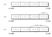
データソースからのデータをバイト単位に分割し、前記バスにローディングするためのデータが、バイト単位であるか、ハーフワード単位であるか、又はワード単位であるかに従って前記分割されたデータのうち、選択されたバイト単位のデータの順序を変換し、選択されないバイト単位のデータを前記変換されたデータに付加して、出力するバイトローテータと、
前記制御信号に応答して前記バイトローテータから入力されるデータのうち前記分割されたデータの前記選択され、順序を変換されたデータを出力し、前記選択されないデータに対しては所定の符号値に変換して出力する符号拡張器と、
前記バス選択信号に応答して前記複数のバスのうち所定のバスを選択し、前記符号拡張器から入力される前記選択されたデータと、前記所定の符号値に変換された出力とを前記選択されたバスにローディングするバス選択回路と、を含むことを特徴とするバス駆動装置。 - 前記選択されるデータの単位はバイト単位、ハーフワード単位及びワード単位のうち一つであることを特徴とする請求項1に記載のバス駆動装置。
- 前記バイトローテータは前記分割されたデータの順序を変換する動作によって前記選択されたバイト単位のデータを全体のデータの下位に位置させることを特徴とする請求項1に記載のバス駆動装置。
- 前記バス選択回路は前記複数のバスと前記符号拡張器との間に連結されて、前記バス選択信号に応答して前記バスを連結、または遮断させるスイッチング素子を含むことを特徴とする請求項1に記載のバス駆動装置。
- 前記スイッチング素子はPMOSトランジスタで構成されることを特徴とする請求項4に記載のバス駆動装置。
- 前記符号拡張器は、前記制御ロジックからの第1選択制御信号に応答して前記バイトローテータから入力されるデータのうち下位一番目のバイトの出力を制御する第1制御回路と、
前記制御ロジックからの第2選択制御信号に応答して前記バイトローテータから入力されるデータのうち下位二番目のバイトの出力を制御する第2制御回路と、
前記制御ロジックからの第3選択制御信号に応答して前記バイトローテータから入力される上位二つのバイトの出力を制御する第3制御回路と、
前記制御ロジックからの符号化制御信号に応答して前記選択されないデータを符号化させる符号化回路とを含むことを特徴とする請求項1に記載のバス駆動装置。 - 前記第1制御回路と前記第2制御回路、前記第3制御回路及び前記符号化回路の最終出力端は前記バスに連結されたNMOSトランジスタを含むことを特徴とする請求項6に記載のバス駆動装置。
- 前記符号化回路は、前記選択されないデータを、前記選択されたデータの最上位のビット値に変換させるか、または全部‘0’の値に符号変換させることを特徴とする請求項6に記載のバス駆動装置。
- 複数のバスを駆動するためのバス駆動方法において、
複数の制御信号とバス選択信号を生成する段階と、
データソースから受信されたデータをバイト単位に分割し、前記バスにローディングするためのデータが、バイト単位であるか、ハーフワード単位であるか、又はワード単位であるかに従って前記分割されたデータのうち、選択されたバイト単位のデータの順序を変換し、選択されないバイト単位のデータを前記変換されたデータに付加して、出力する段階と、
前記制御信号に応答して前記分割されたデータの前記選択され、順序を変換されたデータを出力し、前記選択されないデータに対しては所定の符号値に変換して出力する段階と、
前記バス選択信号に応答して前記複数のバスのうち一つのバスを選択し、前記選択されたバイト単位のデータを前記選択されたバスにローディングする段階とを具備することを特徴とするバス駆動方法。 - 複数のバスを駆動するためのバス駆動装置に使用され、データソースから受信されたデータをバイト単位に分割し、前記バスにローディングするためのデータが、バイト単位であるか、ハーフワード単位であるか、又はワード単位であるかに従って前記分割されたデータのうち、選択されたバイト単位のデータの順序を変換し、選択されないバイト単位のデータを前記変換されたデータに付加して、出力されたデータを入力し、制御ロジックからの制御信号により前記選択されたデータを出力する符号拡張器において、
複数のバイトに分割されたデータのうち下位の一番目のバイトのデータを制御するための第1選択制御信号により制御される第1制御回路と、
複数のバイトに分割された前記データのうち下位二番目のバイトのデータを制御するための第2選択制御信号により制御される第2制御回路と、
複数のバイトに分割された前記データのうち下位三番目のバイトのデータを制御するための第3選択制御信号により制御される第3制御回路と、
前記選択されないバイト単位のデータを符号化させる少なくとも一つの以上の符号化回路とを含むことを特徴とする符号拡張器。 - 前記少なくとも一つの符号化回路は、前記分割されたデータの順序を変換する動作によって選択されたデータの最上位のビット値に前記選択されないデータを変換することを特徴とする請求項10に記載の符号拡張器。
- 前記少なくとも一つの符号化回路は、前記分割されたデータの順序を変換する動作によって前記選択されないデータを全部‘0’の値に変換することを特徴とする請求項10に記載の符号拡張器。
- 前記第1制御回路と前記第2制御回路、前記第3制御回路及び前記符号化回路の最終の出力端は前記バスに連結された少なくとも一つのNMOSトランジスタを含むことを特徴とする請求項10に記載の符号拡張器。
Applications Claiming Priority (2)
| Application Number | Priority Date | Filing Date | Title |
|---|---|---|---|
| KR10-2003-0055076A KR100487569B1 (ko) | 2003-08-08 | 2003-08-08 | 복수의 버스를 구동하는 다중 버스 구동 장치 |
| KR2003-055076 | 2003-08-08 |
Publications (2)
| Publication Number | Publication Date |
|---|---|
| JP2005063410A JP2005063410A (ja) | 2005-03-10 |
| JP4776183B2 true JP4776183B2 (ja) | 2011-09-21 |
Family
ID=34114316
Family Applications (1)
| Application Number | Title | Priority Date | Filing Date |
|---|---|---|---|
| JP2004183964A Expired - Fee Related JP4776183B2 (ja) | 2003-08-08 | 2004-06-22 | 複数のバスを駆動するマルチバス駆動装置 |
Country Status (3)
| Country | Link |
|---|---|
| US (1) | US7263563B2 (ja) |
| JP (1) | JP4776183B2 (ja) |
| KR (1) | KR100487569B1 (ja) |
Family Cites Families (20)
| Publication number | Priority date | Publication date | Assignee | Title |
|---|---|---|---|---|
| US4495598A (en) * | 1982-09-29 | 1985-01-22 | Mcdonnell Douglas Corporation | Computer rotate function |
| US4999808A (en) * | 1986-09-26 | 1991-03-12 | At&T Bell Laboratories | Dual byte order data processor |
| US5265237A (en) * | 1988-12-07 | 1993-11-23 | Xycom, Inc. | Byte swapping apparatus for selectively reordering bytes of an N-bit word communicated between an at computer and VME bus |
| JPH0528107A (ja) | 1991-07-24 | 1993-02-05 | Nec Corp | データバス転送回路 |
| US5410677A (en) * | 1991-12-30 | 1995-04-25 | Apple Computer, Inc. | Apparatus for translating data formats starting at an arbitrary byte position |
| US5585740A (en) * | 1993-12-10 | 1996-12-17 | Ncr Corporation | CMOS low output voltage bus driver with controlled clamps |
| US5751614A (en) * | 1994-03-08 | 1998-05-12 | Exponential Technology, Inc. | Sign-extension merge/mask, rotate/shift, and boolean operations executed in a vectored mux on an ALU |
| US5781457A (en) * | 1994-03-08 | 1998-07-14 | Exponential Technology, Inc. | Merge/mask, rotate/shift, and boolean operations from two instruction sets executed in a vectored mux on a dual-ALU |
| JPH0863267A (ja) * | 1994-08-19 | 1996-03-08 | Hitachi Ltd | 入出力インタフェース回路装置 |
| US5907865A (en) * | 1995-08-28 | 1999-05-25 | Motorola, Inc. | Method and data processing system for dynamically accessing both big-endian and little-endian storage schemes |
| US5646558A (en) * | 1995-09-27 | 1997-07-08 | Intel Corporation | Plurality of distinct multiplexers that operate as a single multiplexer |
| KR0155924B1 (ko) | 1995-11-14 | 1998-11-16 | 김광호 | 버스드라이버 수를 절감한 버스드라이브 회로 |
| JP3462060B2 (ja) * | 1997-11-26 | 2003-11-05 | 株式会社東芝 | 符号拡張回路 |
| KR100295640B1 (ko) * | 1998-01-23 | 2001-08-07 | 김영환 | 버스상호간의데이터제어장치 |
| US6351750B1 (en) * | 1998-10-16 | 2002-02-26 | Softbook Press, Inc. | Dynamic conversion of byte ordering for use on different processor platforms |
| US6347326B1 (en) * | 1999-03-02 | 2002-02-12 | Philips Electronics North America Corporation | N bit by M bit multiplication of twos complement numbers using N/2+1 X M/2+1 bit multipliers |
| US6683530B1 (en) * | 1999-09-08 | 2004-01-27 | Sun Microsystems, Inc. | Method and apparatus for performing a floating point compare operation |
| JP2001195349A (ja) * | 2000-01-14 | 2001-07-19 | Hitachi Ltd | バスアダプタおよびディスク制御装置 |
| US6687262B1 (en) * | 2000-02-21 | 2004-02-03 | Hewlett-Packard Development Company, L.P. | Distributed MUX scheme for bi-endian rotator circuit |
| US6819141B1 (en) * | 2000-03-14 | 2004-11-16 | International Business Machines Corporation | High speed, static digital multiplexer |
-
2003
- 2003-08-08 KR KR10-2003-0055076A patent/KR100487569B1/ko not_active IP Right Cessation
-
2004
- 2004-05-11 US US10/842,522 patent/US7263563B2/en not_active Expired - Fee Related
- 2004-06-22 JP JP2004183964A patent/JP4776183B2/ja not_active Expired - Fee Related
Also Published As
| Publication number | Publication date |
|---|---|
| US20050033868A1 (en) | 2005-02-10 |
| JP2005063410A (ja) | 2005-03-10 |
| KR20050017766A (ko) | 2005-02-23 |
| KR100487569B1 (ko) | 2005-05-03 |
| US7263563B2 (en) | 2007-08-28 |
Similar Documents
| Publication | Publication Date | Title |
|---|---|---|
| JP6207748B2 (ja) | アドレスデコードおよびアクセス線選択のための装置、メモリおよび方法 | |
| KR100530930B1 (ko) | 낸드 플래시 메모리 장치의 멀티-i/o 리페어 방법 및그의 낸드 플래시 메모리 장치 | |
| US7449917B2 (en) | Level shifting circuit for semiconductor device | |
| CN109923611B (zh) | 用于功率高效驱动电路的设备及方法 | |
| JP6158367B2 (ja) | フル・スイング・メモリ・アレイを読み出すための方法及び装置 | |
| JPH10190751A (ja) | 双方向遷移数削減インターフェース回路 | |
| US5224065A (en) | Arithmetic operation unit having bit inversion function | |
| JPH03226016A (ja) | プライオリティ・エンコーダ | |
| JP2009296119A (ja) | 双方向バッファ回路及び信号レベル変換回路 | |
| US6788106B2 (en) | Integrated circuit devices having data inversion circuits therein that reduce simultaneous switching noise and support interleaving of parallel data | |
| KR100298029B1 (ko) | 배럴시프터 | |
| US5416731A (en) | High-speed barrel shifter | |
| JP4776183B2 (ja) | 複数のバスを駆動するマルチバス駆動装置 | |
| US6675182B1 (en) | Method and apparatus for performing rotate operations using cascaded multiplexers | |
| EP0458362B1 (en) | Low power consumption precharge type programmable logic array (PLA) | |
| KR970051273A (ko) | 워드라인 구동 장치 | |
| JPH07153279A (ja) | 多重一致検出装置 | |
| JP3578077B2 (ja) | バレルシフト回路 | |
| US6038229A (en) | Tree switching with fast reconfiguration | |
| KR100411023B1 (ko) | 출력 회로 | |
| US6822486B1 (en) | Multiplexer methods and apparatus | |
| US5724302A (en) | High density decoder | |
| KR100427712B1 (ko) | 트윈컬럼디코더를갖는반도체메모리장치 | |
| JP4687819B2 (ja) | ポストチャージロジックを備えるデータ伝達装置 | |
| JP3393966B2 (ja) | ダイナミック型プライオリティ・エンコーダ |
Legal Events
| Date | Code | Title | Description |
|---|---|---|---|
| A621 | Written request for application examination |
Free format text: JAPANESE INTERMEDIATE CODE: A621 Effective date: 20070316 |
|
| A977 | Report on retrieval |
Free format text: JAPANESE INTERMEDIATE CODE: A971007 Effective date: 20100210 |
|
| A131 | Notification of reasons for refusal |
Free format text: JAPANESE INTERMEDIATE CODE: A131 Effective date: 20100302 |
|
| A521 | Written amendment |
Free format text: JAPANESE INTERMEDIATE CODE: A523 Effective date: 20100531 |
|
| A131 | Notification of reasons for refusal |
Free format text: JAPANESE INTERMEDIATE CODE: A131 Effective date: 20101005 |
|
| A521 | Written amendment |
Free format text: JAPANESE INTERMEDIATE CODE: A523 Effective date: 20101228 |
|
| TRDD | Decision of grant or rejection written | ||
| A01 | Written decision to grant a patent or to grant a registration (utility model) |
Free format text: JAPANESE INTERMEDIATE CODE: A01 Effective date: 20110607 |
|
| A01 | Written decision to grant a patent or to grant a registration (utility model) |
Free format text: JAPANESE INTERMEDIATE CODE: A01 |
|
| A61 | First payment of annual fees (during grant procedure) |
Free format text: JAPANESE INTERMEDIATE CODE: A61 Effective date: 20110628 |
|
| R150 | Certificate of patent or registration of utility model |
Free format text: JAPANESE INTERMEDIATE CODE: R150 |
|
| FPAY | Renewal fee payment (event date is renewal date of database) |
Free format text: PAYMENT UNTIL: 20140708 Year of fee payment: 3 |
|
| LAPS | Cancellation because of no payment of annual fees |