JP4743839B2 - 撮像装置 - Google Patents
撮像装置 Download PDFInfo
- Publication number
- JP4743839B2 JP4743839B2 JP2005038321A JP2005038321A JP4743839B2 JP 4743839 B2 JP4743839 B2 JP 4743839B2 JP 2005038321 A JP2005038321 A JP 2005038321A JP 2005038321 A JP2005038321 A JP 2005038321A JP 4743839 B2 JP4743839 B2 JP 4743839B2
- Authority
- JP
- Japan
- Prior art keywords
- signal
- photoelectric conversion
- conversion unit
- semiconductor region
- reset
- Prior art date
- Legal status (The legal status is an assumption and is not a legal conclusion. Google has not performed a legal analysis and makes no representation as to the accuracy of the status listed.)
- Expired - Fee Related
Links
Images


Classifications
-
- H—ELECTRICITY
- H04—ELECTRIC COMMUNICATION TECHNIQUE
- H04N—PICTORIAL COMMUNICATION, e.g. TELEVISION
- H04N25/00—Circuitry of solid-state image sensors [SSIS]; Control thereof
- H04N25/50—Control of the SSIS exposure
- H04N25/53—Control of the integration time
- H04N25/533—Control of the integration time by using differing integration times for different sensor regions
-
- H—ELECTRICITY
- H04—ELECTRIC COMMUNICATION TECHNIQUE
- H04N—PICTORIAL COMMUNICATION, e.g. TELEVISION
- H04N25/00—Circuitry of solid-state image sensors [SSIS]; Control thereof
- H04N25/50—Control of the SSIS exposure
- H04N25/57—Control of the dynamic range
-
- H—ELECTRICITY
- H04—ELECTRIC COMMUNICATION TECHNIQUE
- H04N—PICTORIAL COMMUNICATION, e.g. TELEVISION
- H04N25/00—Circuitry of solid-state image sensors [SSIS]; Control thereof
- H04N25/50—Control of the SSIS exposure
- H04N25/57—Control of the dynamic range
- H04N25/58—Control of the dynamic range involving two or more exposures
- H04N25/587—Control of the dynamic range involving two or more exposures acquired sequentially, e.g. using the combination of odd and even image fields
-
- H—ELECTRICITY
- H04—ELECTRIC COMMUNICATION TECHNIQUE
- H04N—PICTORIAL COMMUNICATION, e.g. TELEVISION
- H04N25/00—Circuitry of solid-state image sensors [SSIS]; Control thereof
- H04N25/70—SSIS architectures; Circuits associated therewith
- H04N25/76—Addressed sensors, e.g. MOS or CMOS sensors
Landscapes
- Engineering & Computer Science (AREA)
- Multimedia (AREA)
- Signal Processing (AREA)
- Transforming Light Signals Into Electric Signals (AREA)
- Solid State Image Pick-Up Elements (AREA)
Description
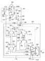
画素構成以外の構成例は実施形態1と同様である。また、駆動シーケンスにおいても実施形態1と同様であるが、φTX2とφRESはφTX2は必ずしも同一の時間帯を持つ必要はない。
301 画素
302 フォトダイオード(光電変換部)
303 転送スイッチ
304 フローティングディフュージョン部(電荷電圧変換部)
305 増幅MOSアンプ
306 選択スイッチ
307 リセットスイッチ
308 転送スイッチ制御部
309 定電流源
310 読み出し部
311 信号読み出し部
312 飽和検出部
313 リセットレベル読み出しスイッチ
314 リセットレベル蓄積容量
315 水平選択スイッチ
316 信号レベル読み出しスイッチ
317 信号レベル蓄積容量
318 水平選択スイッチ
319 差動アンプ
320 比較回路
321 第1比較結果転送スイッチ
322 第1比較メモリ
323 比較結果転送スイッチ
324 第2比較結果転送スイッチ
325 第2比較メモリ
326 第1比較メモリ出力スイッチ
327 第2比較メモリ出力スイッチ
328 飽和検出信号選択回路
329 信号選択回路
330 出力線350 転送制御部
360 垂直信号線
Claims (17)
- 光電変換部と、前記光電変換部で発生した電荷を一時的に蓄積する半導体領域と、前記光電変換部から前記半導体領域に前記電荷を転送する転送スイッチと、前記半導体領域をリセットするリセットスイッチとを備えた少なくとも1つの画素と、
前記半導体領域から信号を読み出す信号読み出し部と、
前記光電変換部の露光期間において、前記転送スイッチがオフの状態で前記光電変換部から前記半導体領域に漏れこんだ電荷量が所定基準量よりも多い場合に、前記転送スイッチと前記リセットスイッチをそれぞれオンすることで前記光電変換部と前記半導体領域をリセットするように制御し、前記光電変換部の露光期間において前記光電変換部から前記半導体領域に漏れ込む電荷量が前記所定基準量よりも少ない場合に、前記転送スイッチをオンしないで前記リセットスイッチをオンすることで前記光電変換部をリセットしないで前記半導体領域をリセットするように制御する制御部と、
を有することを特徴とする撮像装置。 - 前記制御部は、1つの露光期間において、前記半導体領域に生じた信号と基準電位とを比較する比較器による比較動作を少なくとも2回行うように構成されていることを特徴とする請求項1に記載の撮像装置。
- 前記信号読み出し部は、前記転送スイッチによる転送動作に応じて前記半導体領域から読み出される信号と前記転送スイッチによる転送動作前に前記半導体領域から読み出されるリセットレベル信号との差分を画素信号として読み出すように構成され、
前記制御部は、前記比較器による少なくとも2回の比較動作のうち最後の比較動作をリセットレベル信号の読み出し後に行い、前記比較器による少なくとも2回の比較動作のうち最後の比較動作以外の比較動作の結果に応じて前記光電変換部をリセットするように構成されていることを特徴とする請求項2に記載の撮像装置。 - 前記制御部は、前記比較器による比較結果を蓄積するメモリを含むことを特徴とする請求項2又は請求項3に記載の撮像装置。
- 前記制御部は、前記比較器による少なくとも2回の比較動作の結果をそれぞれ蓄積するメモリを含むことを特徴とする請求項2又は請求項3に記載の撮像装置。
- 前記比較器による比較結果を出力する出力回路を更に備えることを特徴とする請求項2乃至請求項5のいずれか1項に記載の撮像装置。
- 前記出力回路は、前記信号読み出し部によって読み出される画素信号と前記比較器による比較結果とを同一の信号線に対して互いに異なる期間に出力するように構成されていることを特徴とする請求項6に記載の撮像装置。
- 前記出力回路は、前記信号読み出し部が1画素の画素信号を出力する期間と次の1画素の画素信号を出力する期間との間の期間において、前記比較器による比較結果を出力するように構成されていることを特徴とする請求項7に記載の撮像装置。
- 前記基準電位を設定可能に構成されていることを特徴とする請求項2乃至請求項8のいずれか1項に記載の撮像装置。
- 前記制御部が前記光電変換部をリセットするタイミングを設定可能に構成されていることを特徴とする請求項1乃至請求項9のいずれか1項に記載の撮像装置。
- 前記制御部は、前記転送スイッチがオフの状態で前記光電変換部から前記半導体領域に漏れこんだ電荷量が前記所定基準量よりも多いことを示す信号と露光期間を制御する転送パルスとの論理和を演算してその演算結果によって前記転送スイッチを制御する転送スイッチ制御部を含むことを特徴とする請求項1乃至請求項10のいずれか1項に記載の撮像装置。
- 前記制御部は、前記転送スイッチと並列に配置された第2転送スイッチを含み、前記転送スイッチは、露光期間を制御する転送パルスによって制御され、前記第2転送スイッチは、前記転送スイッチがオフの状態で前記光電変換部から前記半導体領域に漏れこんだ電荷量が前記所定基準量よりも多いことを示す信号によって制御されることを特徴とする請求項1乃至請求項10のいずれか1項に記載の撮像装置。
- 前記信号読み出し部から出力される信号を処理する信号処理回路を更に備えることを特徴とする請求項1に記載の撮像装置。
- 前記信号処理回路は、前記光電変換部の露光期間において前記光電変換部から前記半導体領域に漏れ込んだ電荷が前記所定基準量よりも多い場合に、前記光電変換部と前記半導体領域のリセット後に前記光電変換部で発生し前記半導体領域に転送された電荷に対応して前記信号読み出し部から出力される信号を補正することを特徴とする請求項13に記載の撮像装置。
- 前記信号処理回路は、前記光電変換部の露光期間において前記光電変換部から前記半導体領域に漏れ込んだ電荷が前記所定基準量よりも多い場合に、前記光電変換部と前記半導体領域のリセット後に前記光電変換部で発生し前記半導体領域に転送された電荷に対応して前記信号読み出し部から出力される信号にゲインを掛けることを特徴とする請求項13に記載の撮像装置。
- 前記信号処理回路は、前記光電変換部の露光期間において前記光電変換部から前記半導体領域に漏れ込む電荷が前記所定基準量よりも多い場合に、前記光電変換部のリセットによる露光期間の短縮分を補うように、前記光電変換部と前記半導体領域のリセット後に前記光電変換部で発生し前記半導体領域に転送された電荷に対応して前記信号読み出し部から出力される信号にゲインを掛けることを特徴とする請求項15に記載の撮像装置。
- 前記信号読み出し部から出力される信号を処理する信号処理回路を更に備え、前記信号処理回路は、前記比較器による少なくとも2回の比較動作のうち最後の比較動作以外の比較動作の結果が、前記光電変換部の露光期間において前記光電変換部から前記半導体領域に漏れ込む電荷が所定基準量よりも多いことを示している場合に、前記光電変換部のリセットによる露光期間の短縮分を補うように、前記光電変換部と前記半導体領域のリセット後に前記光電変換部で発生し前記半導体領域に転送された電荷に対応して前記信号読み出し部から出力される信号にゲインを掛け、前記最後の比較動作の結果が、前記光電変換部の露光期間において前記光電変換部から前記半導体領域に漏れ込む電荷が前記所定基準量よりも多いことを示している場合に、前記光電変換部と前記半導体領域のリセット後に前記光電変換部で発生し前記半導体領域に転送された電荷に対応して前記信号読み出し部から出力される信号を飽和信号によって置き換えることを特徴とする請求項2に記載の撮像装置。
Priority Applications (2)
| Application Number | Priority Date | Filing Date | Title |
|---|---|---|---|
| JP2005038321A JP4743839B2 (ja) | 2005-02-15 | 2005-02-15 | 撮像装置 |
| US11/353,721 US7830439B2 (en) | 2005-02-15 | 2006-02-13 | Image sensing element and processing apparatus |
Applications Claiming Priority (1)
| Application Number | Priority Date | Filing Date | Title |
|---|---|---|---|
| JP2005038321A JP4743839B2 (ja) | 2005-02-15 | 2005-02-15 | 撮像装置 |
Publications (3)
| Publication Number | Publication Date |
|---|---|
| JP2006229362A JP2006229362A (ja) | 2006-08-31 |
| JP2006229362A5 JP2006229362A5 (ja) | 2008-04-03 |
| JP4743839B2 true JP4743839B2 (ja) | 2011-08-10 |
Family
ID=36815235
Family Applications (1)
| Application Number | Title | Priority Date | Filing Date |
|---|---|---|---|
| JP2005038321A Expired - Fee Related JP4743839B2 (ja) | 2005-02-15 | 2005-02-15 | 撮像装置 |
Country Status (2)
| Country | Link |
|---|---|
| US (1) | US7830439B2 (ja) |
| JP (1) | JP4743839B2 (ja) |
Families Citing this family (18)
| Publication number | Priority date | Publication date | Assignee | Title |
|---|---|---|---|---|
| US8184191B2 (en) * | 2006-08-09 | 2012-05-22 | Tohoku University | Optical sensor and solid-state imaging device |
| US7821559B2 (en) * | 2006-10-04 | 2010-10-26 | Canon Kabushiki Kaisha | Photoelectric conversion apparatus provided with arrangement of plurality of pixels each having plurality of photoelectric conversion devices and accumulating unit for temporarily accumulating charges accumulated in plurality of photoelectric conversion devices |
| JP5013811B2 (ja) * | 2006-10-26 | 2012-08-29 | キヤノン株式会社 | 撮像装置及び補正方法 |
| US8203629B2 (en) | 2006-10-26 | 2012-06-19 | Canon Kabushiki Kaisha | Image sensing apparatus and correction method |
| JP5013812B2 (ja) * | 2006-10-26 | 2012-08-29 | キヤノン株式会社 | 撮像装置及び補正方法 |
| JP2008283565A (ja) * | 2007-05-11 | 2008-11-20 | Canon Inc | 撮像素子及び撮像装置 |
| KR101338353B1 (ko) * | 2007-05-30 | 2013-12-06 | 삼성전자주식회사 | 영상 촬상 장치 및 방법 |
| JP4931231B2 (ja) * | 2007-06-25 | 2012-05-16 | キヤノン株式会社 | 撮像装置及びその制御方法 |
| US8063350B2 (en) * | 2007-08-03 | 2011-11-22 | Cognex Corporation | Circuits and methods allowing for pixel array exposure pattern control |
| JP5094324B2 (ja) * | 2007-10-15 | 2012-12-12 | キヤノン株式会社 | 撮像装置 |
| KR101478248B1 (ko) * | 2008-04-11 | 2014-12-31 | 삼성전자주식회사 | 두 개의 게이트로 이루어진 센싱 트랜지스터를 구비한 이미지 센서의 구동방법 |
| FR2943199B1 (fr) * | 2009-03-13 | 2012-12-28 | E2V Semiconductors | Procede de lecture de signal de capteur d'image et capteur d'image. |
| JP5554313B2 (ja) | 2011-11-30 | 2014-07-23 | 富士フイルム株式会社 | 放射線検出器、放射線画像撮影装置、及び放射線画像撮影システム |
| EP2840780A4 (en) * | 2012-04-19 | 2015-08-05 | Univ Tohoku | SEMICONDUCTOR SHOOTING DEVICE |
| EP2874388B1 (en) * | 2013-11-15 | 2019-05-15 | Sony Depthsensing Solutions | Method for avoiding pixel saturation |
| US9342161B2 (en) * | 2014-04-01 | 2016-05-17 | Pixart Imaging Inc. | Optical pointing device and corresponding method for concurrently performing gain control and image capturing for navigation of optical pointing device during one LED turned-on time period |
| US9864437B2 (en) * | 2016-03-22 | 2018-01-09 | Pixart Imaging (Penang) Sdn. Bhd. | Circuit and method for detecting working and resting states for optical mouse |
| CN112887571B (zh) * | 2021-01-27 | 2022-06-10 | 维沃移动通信有限公司 | 图像传感器、摄像模组和电子设备 |
Family Cites Families (22)
| Publication number | Priority date | Publication date | Assignee | Title |
|---|---|---|---|---|
| US4967249A (en) * | 1989-03-17 | 1990-10-30 | Loral Fairchild Corporation | Gain compression photodetector array |
| JP2722784B2 (ja) * | 1990-06-12 | 1998-03-09 | 松下電器産業株式会社 | カラー撮像装置 |
| JP2799072B2 (ja) * | 1990-11-22 | 1998-09-17 | 富士通株式会社 | 撮像装置 |
| JP3166776B2 (ja) * | 1990-11-30 | 2001-05-14 | キヤノン株式会社 | 撮像装置及び撮像方法 |
| JP3484252B2 (ja) * | 1995-02-15 | 2004-01-06 | 日本放送協会 | 固体撮像デバイス |
| US5892541A (en) * | 1996-09-10 | 1999-04-06 | Foveonics, Inc. | Imaging system and method for increasing the dynamic range of an array of active pixel sensor cells |
| JP3724188B2 (ja) | 1998-04-30 | 2005-12-07 | コニカミノルタホールディングス株式会社 | 固体撮像装置 |
| JP3308904B2 (ja) * | 1998-06-24 | 2002-07-29 | キヤノン株式会社 | 固体撮像装置 |
| JP3927696B2 (ja) | 1998-08-05 | 2007-06-13 | キヤノン株式会社 | 撮像装置 |
| WO2000024190A1 (en) * | 1998-10-19 | 2000-04-27 | Ben-Gurion University Of The Negev | Optical imager using a method for adaptive real-time expanding of the dynamic range |
| JP3592107B2 (ja) * | 1998-11-27 | 2004-11-24 | キヤノン株式会社 | 固体撮像装置およびカメラ |
| US6850278B1 (en) * | 1998-11-27 | 2005-02-01 | Canon Kabushiki Kaisha | Solid-state image pickup apparatus |
| JP3517614B2 (ja) | 1998-12-25 | 2004-04-12 | 株式会社東芝 | 固体撮像装置 |
| JP3667220B2 (ja) | 1999-10-05 | 2005-07-06 | キヤノン株式会社 | 固体撮像装置、撮像システム及び固体撮像装置の駆動方法 |
| US6307195B1 (en) * | 1999-10-26 | 2001-10-23 | Eastman Kodak Company | Variable collection of blooming charge to extend dynamic range |
| US6710804B1 (en) * | 2000-01-18 | 2004-03-23 | Eastman Kodak Company | CMOS active pixel image sensor with extended dynamic range and sensitivity |
| JP2002158928A (ja) * | 2000-11-22 | 2002-05-31 | Victor Co Of Japan Ltd | 固体撮像装置 |
| JP3827146B2 (ja) | 2001-09-12 | 2006-09-27 | ソニー株式会社 | 固体撮像装置および固体撮像装置の駆動方法 |
| JP3827145B2 (ja) * | 2001-07-03 | 2006-09-27 | ソニー株式会社 | 固体撮像装置 |
| JP4019409B2 (ja) * | 2001-11-02 | 2007-12-12 | ソニー株式会社 | 固体撮像素子 |
| JP4336544B2 (ja) * | 2003-07-18 | 2009-09-30 | パナソニック株式会社 | 固体撮像装置 |
| JP4389766B2 (ja) * | 2004-11-22 | 2009-12-24 | セイコーエプソン株式会社 | 撮像装置 |
-
2005
- 2005-02-15 JP JP2005038321A patent/JP4743839B2/ja not_active Expired - Fee Related
-
2006
- 2006-02-13 US US11/353,721 patent/US7830439B2/en not_active Expired - Fee Related
Also Published As
| Publication number | Publication date |
|---|---|
| US20060181628A1 (en) | 2006-08-17 |
| US7830439B2 (en) | 2010-11-09 |
| JP2006229362A (ja) | 2006-08-31 |
Similar Documents
| Publication | Publication Date | Title |
|---|---|---|
| US10771718B2 (en) | Imaging device and imaging system | |
| JP4743839B2 (ja) | 撮像装置 | |
| US9894295B2 (en) | Imaging device and imaging system | |
| US9509927B2 (en) | Solid-state imaging device, method of driving the same, signal processing method for the same, and imaging apparatus | |
| US10038868B2 (en) | Solid-state image sensing device and electronic device | |
| US9363450B2 (en) | Imaging systems and methods for image signal gain adjustment | |
| US8294801B2 (en) | Solid-state imaging device, imaging apparatus, pixel driving voltage adjustment apparatus, and pixel driving voltage adjustment method | |
| US9794497B2 (en) | Solid-state imaging device controlling read-out of signals from pixels in first and second areas | |
| US10313588B2 (en) | Image capturing system and control method of image capturing system | |
| US7889247B2 (en) | Solid-state imaging device, method of driving solid-state imaging device, and imaging apparatus | |
| US8179460B2 (en) | System, method, and apparatus for variable rate pixel data transfer and storage | |
| KR101867345B1 (ko) | 픽셀의 구동방법 및 이를 이용하는 cmos 이미지센서 | |
| JP6574653B2 (ja) | 撮像装置及び撮像システム | |
| JP5451052B2 (ja) | 撮像装置 | |
| JP2006191397A (ja) | 固体撮像装置 | |
| JP2009021889A (ja) | 固体撮像装置及びその駆動方法 | |
| JP2011142434A (ja) | 固体撮像装置 | |
| JP4840992B2 (ja) | 光電変換装置及びその制御方法並びに撮像装置 | |
| KR101867344B1 (ko) | 픽셀의 구동방법 및 이를 이용하는 cmos 이미지센서 | |
| US12457434B2 (en) | Image capturing apparatus and control method thereof, image processing apparatus and storage medium | |
| US12425751B2 (en) | Image pickup apparatus in which global shutter driving of image pickup device is performed | |
| JP4840991B2 (ja) | 光電変換装置及びその制御方法並びに撮像装置 | |
| JP2017028513A (ja) | 撮像装置、撮像システム及び信号処理方法 | |
| JP2023111020A (ja) | 撮像素子の制御方法、撮像素子及びプログラム |
Legal Events
| Date | Code | Title | Description |
|---|---|---|---|
| A521 | Request for written amendment filed |
Free format text: JAPANESE INTERMEDIATE CODE: A523 Effective date: 20080214 |
|
| A621 | Written request for application examination |
Free format text: JAPANESE INTERMEDIATE CODE: A621 Effective date: 20080214 |
|
| A977 | Report on retrieval |
Free format text: JAPANESE INTERMEDIATE CODE: A971007 Effective date: 20100525 |
|
| A131 | Notification of reasons for refusal |
Free format text: JAPANESE INTERMEDIATE CODE: A131 Effective date: 20100531 |
|
| A521 | Request for written amendment filed |
Free format text: JAPANESE INTERMEDIATE CODE: A523 Effective date: 20100726 |
|
| TRDD | Decision of grant or rejection written | ||
| A01 | Written decision to grant a patent or to grant a registration (utility model) |
Free format text: JAPANESE INTERMEDIATE CODE: A01 Effective date: 20110428 |
|
| A01 | Written decision to grant a patent or to grant a registration (utility model) |
Free format text: JAPANESE INTERMEDIATE CODE: A01 |
|
| A61 | First payment of annual fees (during grant procedure) |
Free format text: JAPANESE INTERMEDIATE CODE: A61 Effective date: 20110509 |
|
| FPAY | Renewal fee payment (event date is renewal date of database) |
Free format text: PAYMENT UNTIL: 20140520 Year of fee payment: 3 |
|
| R150 | Certificate of patent or registration of utility model |
Free format text: JAPANESE INTERMEDIATE CODE: R150 |
|
| LAPS | Cancellation because of no payment of annual fees |