JP4666783B2 - Method for manufacturing semiconductor device - Google Patents
Method for manufacturing semiconductor device Download PDFInfo
- Publication number
- JP4666783B2 JP4666783B2 JP2001022703A JP2001022703A JP4666783B2 JP 4666783 B2 JP4666783 B2 JP 4666783B2 JP 2001022703 A JP2001022703 A JP 2001022703A JP 2001022703 A JP2001022703 A JP 2001022703A JP 4666783 B2 JP4666783 B2 JP 4666783B2
- Authority
- JP
- Japan
- Prior art keywords
- insulating film
- film
- gate electrode
- semiconductor
- transistor
- Prior art date
- Legal status (The legal status is an assumption and is not a legal conclusion. Google has not performed a legal analysis and makes no representation as to the accuracy of the status listed.)
- Expired - Fee Related
Links
- 239000004065 semiconductor Substances 0.000 title claims description 224
- 238000000034 method Methods 0.000 title claims description 69
- 238000004519 manufacturing process Methods 0.000 title claims description 54
- 230000015654 memory Effects 0.000 claims description 305
- 239000012535 impurity Substances 0.000 claims description 43
- 238000010438 heat treatment Methods 0.000 claims description 16
- OAICVXFJPJFONN-UHFFFAOYSA-N Phosphorus Chemical compound [P] OAICVXFJPJFONN-UHFFFAOYSA-N 0.000 claims description 14
- 229910052698 phosphorus Inorganic materials 0.000 claims description 14
- 239000011574 phosphorus Substances 0.000 claims description 14
- 239000003054 catalyst Substances 0.000 claims description 7
- 230000001681 protective effect Effects 0.000 claims description 7
- 238000005530 etching Methods 0.000 claims description 5
- 230000003197 catalytic effect Effects 0.000 claims description 4
- 239000010408 film Substances 0.000 description 249
- 239000010410 layer Substances 0.000 description 138
- 239000000758 substrate Substances 0.000 description 49
- 229910021417 amorphous silicon Inorganic materials 0.000 description 39
- PXHVJJICTQNCMI-UHFFFAOYSA-N nickel Substances [Ni] PXHVJJICTQNCMI-UHFFFAOYSA-N 0.000 description 22
- 230000015572 biosynthetic process Effects 0.000 description 19
- 230000002093 peripheral effect Effects 0.000 description 19
- XUIMIQQOPSSXEZ-UHFFFAOYSA-N Silicon Chemical compound [Si] XUIMIQQOPSSXEZ-UHFFFAOYSA-N 0.000 description 18
- 230000008569 process Effects 0.000 description 18
- 229910052710 silicon Inorganic materials 0.000 description 18
- 239000010703 silicon Substances 0.000 description 18
- VYPSYNLAJGMNEJ-UHFFFAOYSA-N silicon dioxide Inorganic materials O=[Si]=O VYPSYNLAJGMNEJ-UHFFFAOYSA-N 0.000 description 16
- 239000012298 atmosphere Substances 0.000 description 14
- 238000010586 diagram Methods 0.000 description 13
- 229910052581 Si3N4 Inorganic materials 0.000 description 11
- 238000005247 gettering Methods 0.000 description 11
- HQVNEWCFYHHQES-UHFFFAOYSA-N silicon nitride Chemical compound N12[Si]34N5[Si]62N3[Si]51N64 HQVNEWCFYHHQES-UHFFFAOYSA-N 0.000 description 11
- ZOXJGFHDIHLPTG-UHFFFAOYSA-N Boron Chemical compound [B] ZOXJGFHDIHLPTG-UHFFFAOYSA-N 0.000 description 9
- 229910052796 boron Inorganic materials 0.000 description 9
- 229910052736 halogen Inorganic materials 0.000 description 9
- 150000002367 halogens Chemical class 0.000 description 9
- 239000010453 quartz Substances 0.000 description 9
- 229910052715 tantalum Inorganic materials 0.000 description 9
- 239000010409 thin film Substances 0.000 description 9
- 239000013078 crystal Substances 0.000 description 8
- 229910021419 crystalline silicon Inorganic materials 0.000 description 8
- 239000011229 interlayer Substances 0.000 description 8
- 239000011159 matrix material Substances 0.000 description 8
- 238000004544 sputter deposition Methods 0.000 description 8
- 239000010936 titanium Substances 0.000 description 8
- 229910052721 tungsten Inorganic materials 0.000 description 8
- 239000010937 tungsten Substances 0.000 description 8
- UFHFLCQGNIYNRP-UHFFFAOYSA-N Hydrogen Chemical compound [H][H] UFHFLCQGNIYNRP-UHFFFAOYSA-N 0.000 description 7
- 229910001362 Ta alloys Inorganic materials 0.000 description 7
- 239000011651 chromium Substances 0.000 description 7
- 150000001875 compounds Chemical class 0.000 description 7
- 238000002425 crystallisation Methods 0.000 description 7
- 230000000694 effects Effects 0.000 description 7
- 239000001257 hydrogen Substances 0.000 description 7
- 229910052739 hydrogen Inorganic materials 0.000 description 7
- 239000004973 liquid crystal related substance Substances 0.000 description 7
- 229910052814 silicon oxide Inorganic materials 0.000 description 7
- 238000003860 storage Methods 0.000 description 7
- WFKWXMTUELFFGS-UHFFFAOYSA-N tungsten Chemical compound [W] WFKWXMTUELFFGS-UHFFFAOYSA-N 0.000 description 7
- 229910052751 metal Inorganic materials 0.000 description 6
- 229910052759 nickel Inorganic materials 0.000 description 6
- GUVRBAGPIYLISA-UHFFFAOYSA-N tantalum atom Chemical compound [Ta] GUVRBAGPIYLISA-UHFFFAOYSA-N 0.000 description 6
- VYZAMTAEIAYCRO-UHFFFAOYSA-N Chromium Chemical compound [Cr] VYZAMTAEIAYCRO-UHFFFAOYSA-N 0.000 description 5
- ZOKXTWBITQBERF-UHFFFAOYSA-N Molybdenum Chemical compound [Mo] ZOKXTWBITQBERF-UHFFFAOYSA-N 0.000 description 5
- 229910052804 chromium Inorganic materials 0.000 description 5
- 238000005516 engineering process Methods 0.000 description 5
- 238000005984 hydrogenation reaction Methods 0.000 description 5
- 229910052750 molybdenum Inorganic materials 0.000 description 5
- 239000011733 molybdenum Substances 0.000 description 5
- 238000007254 oxidation reaction Methods 0.000 description 5
- LEVVHYCKPQWKOP-UHFFFAOYSA-N [Si].[Ge] Chemical compound [Si].[Ge] LEVVHYCKPQWKOP-UHFFFAOYSA-N 0.000 description 4
- 230000006866 deterioration Effects 0.000 description 4
- 229910052738 indium Inorganic materials 0.000 description 4
- APFVFJFRJDLVQX-UHFFFAOYSA-N indium atom Chemical compound [In] APFVFJFRJDLVQX-UHFFFAOYSA-N 0.000 description 4
- 230000003647 oxidation Effects 0.000 description 4
- 238000005268 plasma chemical vapour deposition Methods 0.000 description 4
- GYHNNYVSQQEPJS-UHFFFAOYSA-N Gallium Chemical compound [Ga] GYHNNYVSQQEPJS-UHFFFAOYSA-N 0.000 description 3
- VEXZGXHMUGYJMC-UHFFFAOYSA-N Hydrochloric acid Chemical compound Cl VEXZGXHMUGYJMC-UHFFFAOYSA-N 0.000 description 3
- XEEYBQQBJWHFJM-UHFFFAOYSA-N Iron Chemical compound [Fe] XEEYBQQBJWHFJM-UHFFFAOYSA-N 0.000 description 3
- KDLHZDBZIXYQEI-UHFFFAOYSA-N Palladium Chemical compound [Pd] KDLHZDBZIXYQEI-UHFFFAOYSA-N 0.000 description 3
- RTAQQCXQSZGOHL-UHFFFAOYSA-N Titanium Chemical compound [Ti] RTAQQCXQSZGOHL-UHFFFAOYSA-N 0.000 description 3
- 230000001133 acceleration Effects 0.000 description 3
- 229910052782 aluminium Inorganic materials 0.000 description 3
- XAGFODPZIPBFFR-UHFFFAOYSA-N aluminium Chemical compound [Al] XAGFODPZIPBFFR-UHFFFAOYSA-N 0.000 description 3
- 238000000137 annealing Methods 0.000 description 3
- QVGXLLKOCUKJST-UHFFFAOYSA-N atomic oxygen Chemical compound [O] QVGXLLKOCUKJST-UHFFFAOYSA-N 0.000 description 3
- 230000008025 crystallization Effects 0.000 description 3
- 238000001312 dry etching Methods 0.000 description 3
- 229910052733 gallium Inorganic materials 0.000 description 3
- 239000007789 gas Substances 0.000 description 3
- 238000005224 laser annealing Methods 0.000 description 3
- 239000002184 metal Substances 0.000 description 3
- 239000001301 oxygen Substances 0.000 description 3
- 229910052760 oxygen Inorganic materials 0.000 description 3
- BASFCYQUMIYNBI-UHFFFAOYSA-N platinum Chemical compound [Pt] BASFCYQUMIYNBI-UHFFFAOYSA-N 0.000 description 3
- 229910052719 titanium Inorganic materials 0.000 description 3
- 229910000838 Al alloy Inorganic materials 0.000 description 2
- 230000004913 activation Effects 0.000 description 2
- 230000002411 adverse Effects 0.000 description 2
- 229910045601 alloy Inorganic materials 0.000 description 2
- 239000000956 alloy Substances 0.000 description 2
- 238000004458 analytical method Methods 0.000 description 2
- 229910052785 arsenic Inorganic materials 0.000 description 2
- RQNWIZPPADIBDY-UHFFFAOYSA-N arsenic atom Chemical compound [As] RQNWIZPPADIBDY-UHFFFAOYSA-N 0.000 description 2
- IVHJCRXBQPGLOV-UHFFFAOYSA-N azanylidynetungsten Chemical compound [W]#N IVHJCRXBQPGLOV-UHFFFAOYSA-N 0.000 description 2
- 239000000969 carrier Substances 0.000 description 2
- 239000000460 chlorine Substances 0.000 description 2
- 239000010949 copper Substances 0.000 description 2
- 230000007547 defect Effects 0.000 description 2
- 239000010931 gold Substances 0.000 description 2
- 239000002784 hot electron Substances 0.000 description 2
- 229910000041 hydrogen chloride Inorganic materials 0.000 description 2
- IXCSERBJSXMMFS-UHFFFAOYSA-N hydrogen chloride Substances Cl.Cl IXCSERBJSXMMFS-UHFFFAOYSA-N 0.000 description 2
- 239000011261 inert gas Substances 0.000 description 2
- 238000009413 insulation Methods 0.000 description 2
- 239000012212 insulator Substances 0.000 description 2
- 150000002500 ions Chemical group 0.000 description 2
- 239000000463 material Substances 0.000 description 2
- 229910052754 neon Inorganic materials 0.000 description 2
- GKAOGPIIYCISHV-UHFFFAOYSA-N neon atom Chemical compound [Ne] GKAOGPIIYCISHV-UHFFFAOYSA-N 0.000 description 2
- 150000004767 nitrides Chemical class 0.000 description 2
- 230000003287 optical effect Effects 0.000 description 2
- 230000001590 oxidative effect Effects 0.000 description 2
- 238000000059 patterning Methods 0.000 description 2
- 238000005498 polishing Methods 0.000 description 2
- 239000011347 resin Substances 0.000 description 2
- 229920005989 resin Polymers 0.000 description 2
- 229910021332 silicide Inorganic materials 0.000 description 2
- FVBUAEGBCNSCDD-UHFFFAOYSA-N silicide(4-) Chemical compound [Si-4] FVBUAEGBCNSCDD-UHFFFAOYSA-N 0.000 description 2
- 239000002356 single layer Substances 0.000 description 2
- 239000000243 solution Substances 0.000 description 2
- 238000004528 spin coating Methods 0.000 description 2
- 239000012808 vapor phase Substances 0.000 description 2
- 238000001039 wet etching Methods 0.000 description 2
- 229910052724 xenon Inorganic materials 0.000 description 2
- FHNFHKCVQCLJFQ-UHFFFAOYSA-N xenon atom Chemical compound [Xe] FHNFHKCVQCLJFQ-UHFFFAOYSA-N 0.000 description 2
- ZAMOUSCENKQFHK-UHFFFAOYSA-N Chlorine atom Chemical compound [Cl] ZAMOUSCENKQFHK-UHFFFAOYSA-N 0.000 description 1
- RYGMFSIKBFXOCR-UHFFFAOYSA-N Copper Chemical compound [Cu] RYGMFSIKBFXOCR-UHFFFAOYSA-N 0.000 description 1
- YCKRFDGAMUMZLT-UHFFFAOYSA-N Fluorine atom Chemical compound [F] YCKRFDGAMUMZLT-UHFFFAOYSA-N 0.000 description 1
- 229910021586 Nickel(II) chloride Inorganic materials 0.000 description 1
- GRYLNZFGIOXLOG-UHFFFAOYSA-N Nitric acid Chemical compound O[N+]([O-])=O GRYLNZFGIOXLOG-UHFFFAOYSA-N 0.000 description 1
- NRTOMJZYCJJWKI-UHFFFAOYSA-N Titanium nitride Chemical compound [Ti]#N NRTOMJZYCJJWKI-UHFFFAOYSA-N 0.000 description 1
- 229910001080 W alloy Inorganic materials 0.000 description 1
- 239000002253 acid Substances 0.000 description 1
- 230000009471 action Effects 0.000 description 1
- 230000004888 barrier function Effects 0.000 description 1
- 230000008901 benefit Effects 0.000 description 1
- 239000000919 ceramic Substances 0.000 description 1
- 229910052801 chlorine Inorganic materials 0.000 description 1
- 239000010941 cobalt Substances 0.000 description 1
- 229910017052 cobalt Inorganic materials 0.000 description 1
- GUTLYIVDDKVIGB-UHFFFAOYSA-N cobalt atom Chemical group [Co] GUTLYIVDDKVIGB-UHFFFAOYSA-N 0.000 description 1
- 239000000470 constituent Substances 0.000 description 1
- 238000011109 contamination Methods 0.000 description 1
- 229910052802 copper Inorganic materials 0.000 description 1
- 238000000354 decomposition reaction Methods 0.000 description 1
- 238000005401 electroluminescence Methods 0.000 description 1
- 230000001747 exhibiting effect Effects 0.000 description 1
- 229910052731 fluorine Inorganic materials 0.000 description 1
- 239000011737 fluorine Substances 0.000 description 1
- 230000006870 function Effects 0.000 description 1
- 229910052732 germanium Inorganic materials 0.000 description 1
- GNPVGFCGXDBREM-UHFFFAOYSA-N germanium atom Chemical compound [Ge] GNPVGFCGXDBREM-UHFFFAOYSA-N 0.000 description 1
- 239000011521 glass Substances 0.000 description 1
- PCHJSUWPFVWCPO-UHFFFAOYSA-N gold Chemical compound [Au] PCHJSUWPFVWCPO-UHFFFAOYSA-N 0.000 description 1
- 229910052737 gold Inorganic materials 0.000 description 1
- 150000002366 halogen compounds Chemical group 0.000 description 1
- 238000002513 implantation Methods 0.000 description 1
- 238000002347 injection Methods 0.000 description 1
- 239000007924 injection Substances 0.000 description 1
- 238000005468 ion implantation Methods 0.000 description 1
- 229910052742 iron Inorganic materials 0.000 description 1
- 230000014759 maintenance of location Effects 0.000 description 1
- 238000005259 measurement Methods 0.000 description 1
- 229910001507 metal halide Inorganic materials 0.000 description 1
- 150000005309 metal halides Chemical class 0.000 description 1
- QMMRZOWCJAIUJA-UHFFFAOYSA-L nickel dichloride Chemical compound Cl[Ni]Cl QMMRZOWCJAIUJA-UHFFFAOYSA-L 0.000 description 1
- 229910017604 nitric acid Inorganic materials 0.000 description 1
- 239000012299 nitrogen atmosphere Substances 0.000 description 1
- 229910052763 palladium Inorganic materials 0.000 description 1
- 229910052697 platinum Inorganic materials 0.000 description 1
- 230000004044 response Effects 0.000 description 1
- 230000000630 rising effect Effects 0.000 description 1
- 238000009751 slip forming Methods 0.000 description 1
- 239000000126 substance Substances 0.000 description 1
- 239000000725 suspension Substances 0.000 description 1
- MZLGASXMSKOWSE-UHFFFAOYSA-N tantalum nitride Chemical compound [Ta]#N MZLGASXMSKOWSE-UHFFFAOYSA-N 0.000 description 1
- 229910021341 titanium silicide Inorganic materials 0.000 description 1
- WQJQOUPTWCFRMM-UHFFFAOYSA-N tungsten disilicide Chemical compound [Si]#[W]#[Si] WQJQOUPTWCFRMM-UHFFFAOYSA-N 0.000 description 1
- -1 tungsten nitride Chemical class 0.000 description 1
- 229910021342 tungsten silicide Inorganic materials 0.000 description 1
Images


Landscapes
- Liquid Crystal (AREA)
- Non-Volatile Memory (AREA)
- Thin Film Transistor (AREA)
- Read Only Memory (AREA)
- Devices For Indicating Variable Information By Combining Individual Elements (AREA)
- Semiconductor Memories (AREA)
Description
【0001】
【発明が属する技術分野】
本願発明はSOI(Silicon On Insulator)技術を用いて形成される薄膜トランジスタ(以下TFTという)で構成された不揮発性メモリおよびその作製方法に関する。特に、その駆動回路などの周辺回路と共に絶縁表面を有する基板上に一体形成された不揮発性メモリ、特にEEPROM(Electrically Erasable and Programmable Read Only Memory)に関する。また、薄膜トランジスタ(TFT)で構成された任意の回路と共に絶縁表面を有する基板上に一体形成された不揮発性メモリを具備する半導体装置に関する。
【0002】
なお、本願明細書において半導体装置とは、半導体特性を利用することで機能する装置全般を指し、例えば、液晶表示装置およびEL表示装置に代表される電気光学装置および電気光学装置を搭載した電子機器をその範疇に含んでいる。
【0003】
【従来の技術】
近年、急速に半導体装置の多機能化、高機能化かつ小型化が進んでおり、それに伴い、様々な半導体装置におけるメモリ使用頻度が増大してきている。そして、そのような需要を背景として、高性能、高記憶容量、高信頼性、かつ小型のメモリが要求されてきた。
【0004】
現在、半導体装置の記憶装置としては、磁気ディスクやバルクシリコンで作製された半導体不揮発性メモリが最もよく用いられている。
【0005】
磁気ディスクは、半導体装置に用いられる記憶装置の中で、最も記憶容量が大きいものの一つであるが、小型化が困難で、かつ、書き込み/読み出し速度が遅いという欠点がある。
【0006】
一方、半導体不揮発性メモリは、現在記憶容量に関しては磁気ディスクに劣るものの、その書き込み/読み出し速度は、磁気ディスクの数十倍である。また、半導体不揮発性メモリは、書き換え回数やデータ保持時間に関しても十分な性能を有するものが開発されてきている。このような背景から、最近半導体メモリを磁気ディスクの代替品として用いる動きが高まってきた。
【0007】
【発明が解決しようとする課題】
従来の半導体不揮発性メモリは、バルクシリコンを用いて作製され、パッケージに収められているため、このような半導体不揮発性メモリを半導体装置に搭載する場合、工程が増加し、かつそのパッケージサイズのために半導体装置の小型化に支障をきたしていた。
【0008】
本願発明は、上記の事情を鑑みてなされたものであり、他の半導体装置の部品と一体形成され得、小型化が可能な不揮発性メモリを提供することを課題とする。また、小型化が可能な、不揮発性メモリを具備する半導体装置を提供することを課題とする。
【0009】
【課題を解決するための手段】
上記課題を解決するための手段として、本願発明では、不揮発性メモリをSOI(Silicon On Insulator)技術を用いて形成される薄膜トランジスタ(TFT)を用いて構成する。
【0010】
本願発明により、不揮発性メモリは、薄膜トランジスタ(TFT)で構成された任意の回路と共に絶縁基板上に一体形成が可能となる。特に、メモリセル、その駆動回路(代表的には、アドレスデコーダ)およびその他の周辺回路とを絶縁基板上に一体形成することにより、小型化が可能な不揮発性メモリを提供することが可能となる。またさらに、他の半導体装置を構成する、TFTで構成された任意の回路と共に絶縁基板上に一体形成することにより、小型化が可能な、不揮発性メモリを備えた半導体装置を提供することが可能となる。
【0011】
具体的には、本願発明の不揮発性メモリは、メモリセルがマトリクス状に配置されたメモリセルアレイを有し、各メモリセルはメモリTFTとスイッチングTFTとを含む。また、メモリセルの駆動回路およびその他の周辺回路を含んでいてもよい。
【0012】
本願発明において、各メモリセルを構成するメモリTFTとスイッチングTFTの半導体活性層は、連続的につながっている。言い換えると、各メモリセルが有するメモリTFTとスイッチングTFTは、同じ半導体活性層上に形成される。このような構造をとることにより、各メモリセルを構成するメモリTFTとスイッチングTFTとを別々の半導体活性層上に形成した場合と比べて、メモリセル面積の縮小を図ることができる。
【0013】
また、メモリTFTの半導体活性層は、スイッチングTFTの半導体活性層よりも薄く、或は、膜厚が1〜100nm(好ましくは1〜50nm、より好ましくは10〜40nm)となるように形成される。このようにメモリTFTの半導体活性層を薄く形成することにより、膜厚が厚い場合と比べて効率的な書き込みが可能となる。このことはまた、より低駆動電圧での書き込みが可能であることを意味し、同時に、より多い書き換え回数に耐え得る構造となる。
【0014】
また、本願発明の不揮発性メモリの作製工程には、絶縁基板上に第1の非晶質半導体層と、第2の非晶質半導体層とを形成する工程と、これらの非晶質半導体層を結晶化させ、第1の膜厚を有する領域と第2の膜厚を有する領域とからなる結晶性半導体層を形成する工程と、が含まれる。
【0015】
このように形成された結晶性半導体層内において、第1の膜厚を有する領域を半導体活性層とするメモリTFTを形成し、第2の膜厚を有する領域を半導体活性層とするスイッチングTFTを形成することにより、メモリTFTとスイッチングTFTの半導体活性層が連続的につながったメモリセルを有する、不揮発性メモリを作製することが可能となる。さらに、第1の膜厚を第2の膜厚より薄く、あるいは、第1の膜厚が1〜100nm(好ましくは1〜50nm、より好ましくは10〜40nm)となるように形成することにより、本願発明の不揮発性メモリを作製することが可能となる。
【0016】
以下に、本願発明の構成を示す。
【0017】
メモリTFTとスイッチングTFTとから成るメモリセルがマトリクス状に配置されたメモリセルアレイを少なくとも備えた不揮発性メモリであって、
前記メモリTFTは、絶縁基板上に形成される第1の半導体活性層と、第1の絶縁膜と、フローティングゲート電極と、第2の絶縁膜と、コントロールゲート電極と、を少なくとも備えており、
前記スイッチングTFTは、前記絶縁基板上に形成される第2の半導体活性層と、ゲート絶縁膜と、ゲート電極と、を少なくとも備えており、
前記メモリTFTと前記スイッチングTFTとは、前記絶縁基板上に一体形成され、
前記第1の半導体活性層と前記第2の半導体活性層とは、連続的につながっており、
前記第1の半導体活性層の厚さは、前記第2の半導体活性層の厚さよりも薄いことを特徴とする不揮発性メモリが提供される。
【0018】
前記第1及び第2の半導体活性層の厚さは、1〜150nmであることが好ましい。
【0019】
メモリTFTとスイッチングTFTとから成るメモリセルがマトリクス状に配置された不揮発性メモリであって、
前記メモリTFTは、絶縁基板上に形成される第1の半導体活性層と、第1の絶縁膜と、フローティングゲート電極と、第2の絶縁膜と、コントロールゲート電極と、を少なくとも備えており、
前記スイッチングTFTは、前記絶縁基板上に形成される第2の半導体活性層と、ゲート絶縁膜と、ゲート電極と、を少なくとも備えており、
前記メモリTFTと前記スイッチングTFTとは、前記絶縁基板上に一体形成され、
前記第1の半導体活性層と前記第2の半導体活性層とは、連続的につながっており、
前記第1の半導体活性層の厚さは、1〜100nmであり、前記第2の半導体活性層の厚さは、1〜150nmであることを特徴とする不揮発性メモリが提供される。
【0020】
前記第1の半導体活性層の厚さは1〜50nmであり、前記第2の半導体活性層の厚さは10〜100nmであることが好ましい。
【0021】
前記第1の半導体活性層の厚さは10〜40nmであることがより好ましい。
【0022】
前記第1の半導体活性層は、前記第2の半導体活性層よりも、インパクトイオン化が起こりやすい厚さを有することが好ましい。
【0023】
前記メモリTFTのフローティングゲート電極と第1の半導体活性層との間に流れる第1のトンネル電流は、前記スイッチングTFTのゲート電極と第2の半導体活性層との間に流れる第2のトンネル電流の2倍以上であることが好ましい。
【0024】
前記メモリTFT及び前記スイッチングTFTは、pチャネル型TFTであることが好ましい。
【0025】
メモリセルの駆動回路を少なくとも備えており、前記メモリセルアレイと前記メモリセルの駆動回路とは、前記絶縁基板上に一体形成されることを特徴とする不揮発性メモリが提供される。
【0026】
絶縁基板上に複数の画素TFTがマトリクス状に配置された画素回路と、前記複数の画素TFTを駆動するTFTで構成された駆動回路と、前記不揮発性メモリと、を少なくとも備えた半導体装置であって、
前記画素回路と前記駆動回路と前記不揮発性メモリとは、前記絶縁基板上に一体形成される半導体装置が提供される。
【0027】
前記半導体装置として、液晶表示装置、或いはEL(electroluminescence)表示装置等が提供される。EL表示装置とは発光装置または発光ダイオードとも呼ばれる。また、本明細書のEL装置はトリプレット及びシングレットの発光装置も含まれる。
【0028】
前記半導体装置として、ディスプレイ、ビデオカメラ、ヘッドマウントディスプレイ、DVDプレーヤー、ゴーグル型ディスプレイ、パーソナルコンピュータ、携帯電話、カーオーディオ等が提供される。
【0029】
メモリTFTとスイッチングTFTとから成るメモリセルがマトリクス状に配置されたメモリセルアレイを少なくとも備えた不揮発性メモリの作製方法であって、
絶縁基板上に第1の非晶質半導体層と、第2の非晶質半導体層とを形成する工程と、
前記第1の非晶質半導体層と、前記第2の非晶質半導体層とを結晶化させ、第1の膜厚を有する領域と第2の膜厚を有する領域とからなる結晶性半導体層を形成する工程と、
前記結晶性半導体層内において、前記第1の膜厚を有する領域を第1の半導体活性層とするメモリTFTを形成する工程と、前記第2の膜厚を有する領域を第2の半導体活性層とするスイッチングTFTを形成する工程と、
を含む不揮発性メモリの作製方法であって、
前記第1の膜厚は、前記第2の膜厚よりも薄いことを特徴とする不揮発性メモリの作製方法が提供される。
【0030】
前記不揮発性メモリの作製方法において、前記第1及び第2の膜厚は、1〜150nmであることが好ましい。
【0031】
メモリTFTとスイッチングTFTとから成るメモリセルがマトリクス状に配置されたメモリセルアレイを少なくとも備えた不揮発性メモリの作製方法であって、
絶縁基板上に第1の非晶質半導体層と、第2の非晶質半導体層とを形成する工程と、
前記第1の非晶質半導体層と、前記第2の非晶質半導体層とを結晶化させ、第1の膜厚を有する領域と第2の膜厚を有する領域とからなる結晶性半導体層を形成する工程と、
前記結晶性半導体層内において、前記第1の膜厚を有する領域を第1の半導体活性層とするメモリTFTを形成する工程と、
前記第2の膜厚を有する領域を第2の半導体活性層とするスイッチングTFTを形成する工程と、
を含む不揮発性メモリの作製方法であって、
前記第1の膜厚は、1〜100nmであり、前記第2の膜厚は、1〜150nmであることを特徴とする不揮発性メモリの作製方法が提供される。
【0032】
前記不揮発性メモリの作製方法において、前記第1の膜厚は1〜50nmであり、前記第2の膜厚は10〜100nmであることが好ましい。
【0033】
前記不揮発性メモリの作製方法において、前記第1の膜厚は10〜40nmであることがより好ましい。
【0034】
前記不揮発性メモリの作製方法において、前記第1の半導体活性層は、前記第2の半導体活性層よりも、インパクトイオン化が起こりやすい厚さを有することが好ましい。
【0035】
前記不揮発性メモリの作製方法において、前記メモリTFTのフローティングゲート電極と第1の半導体活性層との間に流れる第1のトンネル電流は、前記スイッチングTFTのゲート電極と第2の半導体活性層との間に流れる第2のトンネル電流の2倍以上であることが好ましい。
【0036】
前記不揮発性メモリの作製方法において、前記メモリTFT及び前記スイッチングTFTは、pチャネル型TFTであることが好ましい。
【0037】
メモリセルの駆動回路を少なくとも備えており、前記メモリセルアレイと前記メモリセルの駆動回路とは、前記絶縁基板上に一体形成されることを特徴とする不揮発性メモリの作製方法が提供される。
【0038】
前期不揮発性メモリの作製方法を用いる半導体装置の作製方法であって、
前記半導体装置は、画素部と、前記画素部を駆動する駆動回路と、前記不揮発性メモリの作製方法によって作製される不揮発性メモリと、を少なくとも備えており、
前記画素部と前記駆動回路と前記不揮発性メモリとは、絶縁基板上に一体形成されることを特徴とする半導体装置の作製方法が提供される。
【0039】
前記半導体装置の作製方法として、液晶表示装置、或いはEL表示装置等の作製方法が提供される。
【0040】
前記半導体装置の作製方法として、ディスプレイ、ビデオカメラ、ヘッドマウントディスプレイ、DVDプレーヤー、ゴーグル型ディスプレイ、パーソナルコンピュータ、携帯電話、カーオーディオ等の作製方法が提供される。
【0041】
【発明の実施の形態】
以下に、本願発明の不揮発性メモリの回路図及びその駆動方法を、m×nビットの場合について説明する。また、不揮発性メモリを構成するメモリセルの上面構造、及び断面構造についても、例を挙げて説明する。
【0042】
また、本願発明の不揮発性メモリの作製方法についても簡単に説明する。なお、作製方法については実施例1及び2で詳しく説明する。
【0043】
なお、本実施の形態における不揮発性メモリは、その駆動回路(本実施の形態では、アドレスデコーダ)、および他の周辺回路と共に、さらに場合によっては、半導体装置の他の部品と共に、絶縁基板上に一体形成される。また、本実施の形態では、不揮発性メモリとして、特にEEPROM(Electrically Erasable and Programmable Read Only Memory)について述べる。
【0044】
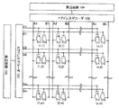
図1に本願発明におけるm×nビット不揮発性メモリの回路図を示す。本実施の形態において、m×nビット不揮発性メモリは、複数の電気的消去可能なメモリTFT(メモリ素子、記憶素子)Tr1、複数のスイッチングTFTTr2、Xアドレスデコーダ101、Yアドレスデコーダ102、および他の周辺回路103、104によって構成される。他の周辺回路には、アドレスバッファ回路やコントロールロジック回路などが含まれ、必要に応じて設けられる。メモリTFTTr1は、フローティングゲートを有するTFTであり、1ビットのデータが記録される。また、本願発明において、メモリTFTTr1とスイッチングTFTTr2とは、同じ導電型TFTであることが必要である。なお、メモリTFTTr1とスイッチングTFTTr2はnチャネル型またはpチャネル型のいずれの導電型TFTでも良いが、pチャネル型TFTであることが好ましい。
【0045】
メモリTFTTr1のソース電極と、スイッチングTFTTr2のドレイン電極は電気的に接続されており、この2個のTFTの直列接続回路によって1ビットのメモリセルが構成される。本実施の形態では、このメモリセルが縦m個×横n個のマトリクス状に配列されている(m、nはそれぞれ1以上の整数)。各メモリセルは1ビットの情報を記憶することができるので、本実施の形態の不揮発性メモリは、m×nビットの記憶容量を有する。
【0046】
図1に示されるように、m×nビット不揮発性メモリを構成する各メモリセルには、(1、1)、(2、1)〜(n、m)という符号が付けられている。そして、各列に配置されているメモリセルは、A1、B1〜An、Bnという符号が付けられている信号線にその両端が接続されており、各行に配列されているメモリセルには、信号線C1、D1〜Cm、Dmが接続されている。具体的には、i番目の列に配置されている各メモリセル(i、1)、(i、2)〜(i、m)が有するメモリTFTTr1のドレイン電極に信号線Aiが接続され、スイッチングTFTのソース電極に信号線Biが接続されている(iは1以上n以下の整数)。また、j番目の行に配置されているメモリセル(1、j)、(2、j)〜(n、j)が有するメモリTFTTr1のコントロールゲート電極に信号線Cjが接続され、スイッチングTFTTr2のゲート電極に信号線Djが接続されている(jは1以上m以下の整数)。
【0047】
各信号線A1、B1〜An、Bn、およびC1、D1〜Cm、Dmは、それぞれXアドレスデコーダ101、およびYアドレスデコーダ102に接続されている。このXアドレスデコーダ101およびYアドレスデコーダ102によって、特定のメモリセルが指定され、データの書き込み、読み出し、および消去が行われる。
【0048】
ここで、本実施の形態の不揮発性メモリの動作について、図1におけるメモリセル(1、1)を例にとって説明する。
【0049】
まず、メモリTFTTr1にデータを書き込む場合は、信号線D1を介して、スイッチングTFTTr2をオンの状態にする。また、信号線A1とB1を介して、メモリTFTTr1のドレイン電極とスイッチングTFTTr2のソース電極の間に適度な電位差を与える。そして、信号線C1を介してメモリTFTTr1コントロールゲートに正の高電圧(例えば20V)を印加するとメモリTFTTr1のチャネル形成領域を移動するキャリア(この場合はホール)が加速され、弱いアバランシェ崩壊またはインパクトイオン化が起こり、多数の高エネルギー状態の電子(ホットエレクトロン)が発生する。そして、ホットエレクトロンはゲート絶縁膜のエネルギー障壁を乗り越え、フローティングゲート電極に注入される。このようにしてフローティングゲート電極に電荷が蓄積され、書き込みが行われる。メモリTFTTr1のしきい値電圧は、フローティングゲート電極に蓄積された電荷量に依存して変化する。
【0050】
メモリセルからデータを読み出す場合は、例えば、信号線D1を介してスイッチングTFTTr2をオンの状態にし、信号線C1を介してメモリTFTTr1のコントロールゲートに0Vを印加し、信号線B1を介してスイッチングTFTTr2のソースをGNDにおとすとよい。その結果、メモリTFTTr1のフローティングゲート電極に蓄積された電荷に応じて、メモリTFTTr1の導通または非導通が決まり、メモリセルに記憶されているデータが信号線A1から読み出される。
【0051】
次に、メモリTFTTr1に記憶されているデータを消去する場合、信号線D1を介してスイッチングTFTTr2をオンの状態にし、信号線B1介してスイッチングTFTTR1のソース電極をGNDにおとす。そして、信号線C1に負の高電圧(例えば−20V)を印加すると、フローティングゲート電極にトラップされている電子がトンネル電流によってドレイン領域へ放出される。その結果、記憶されていたデータが消去される。
【0052】
表1に、上述した動作に基づいて、信号線A1、B1、C1およびD1に印加される電圧の具体例を示す。なお、メモリTFTTr1とスイッチングTFTTr2はいずれもpチャネル型TFTであるとする。
【0053】
【表1】

なお、表1に示した信号線に印加される電圧は、一例であって、表1の値に限られるわけではない。例えば、メモリTFTに印加される電圧は、メモリTFTの半導体活性層の膜厚やコントロールゲート電極とフローティングゲート電極との間の容量等に依存する。そしてメモリTFTの動作電圧もそれに従って変化する。
【0055】
また、メモリTFTTr1とスイッチングTFTTr2がnチャネル型TFTであってもよい。その場合は、例えば、信号線D1に印加する電圧を全て+5Vとすればよい。なお、メモリTFTにnチャネル型TFTを用いた場合には、pチャネル型TFTを用いた場合よりも、書き込み時に大きな電流が流れ、劣化がはやい場合がある。従って、本実施の形態においては、メモリTFTTr1はpチャネル型であることが好ましい。
【0056】
また、本実施の形態において、メモリTFTの書き込み/消去を行う場合、メモリTFTのコントロ─ルゲート電極に一度に+20/−20Vの電圧を印加するのではなく、これよりも低い電圧を複数回のパルスで印加してもよい。この場合、TFTの劣化をある程度抑えることが出来る。
【0057】
次に、本願発明の不揮発性メモリを構成するメモリセルの上面構造、及び断面構造について、図7及び図2を用いて説明する。
【0058】
まず、本願発明の不揮発性メモリを構成するメモリセルの上面図の一例を示す。図7には、4つのメモリセル(1、1)、(1、2)、(2、1)、(2、2)(図1参照)を含む領域の上面図が示されている。
【0059】
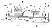
図7において、領域701〜704は半導体活性層であり、メモリTFTTr1およびスイッチングTFTTr2を同一の半導体活性層上に構成している。第1の配線層711〜714のうち、配線713、714はスイッチングTFTTr2のゲート電極および信号線C1、C2として用いられ、また配線711、712は、信号線D1、D2として用いられる。なお、メモリTFTTr1のフローティングゲート電極715〜718は、第1の配線層711〜714と同時に形成される。第2の配線層731〜738のうち、配線731、732は、メモリTFTTr1のソース領域に接続される信号線A1、A2として用いられ、配線733、734はスイッチングTFTTr2のドレイン領域に接続される信号線B1、B2として用いられる。また、配線735〜738はメモリTFTTr1のコントロールゲート電極721〜724と信号線D1、D2とを接続する配線として用いられる。また、図中において、黒く塗りつぶされている部分は、その下部の配線あるいは半導体層とコンタクトをとっていることを示している。なお、図中において同一柄の配線は全て同一の配線層である。
【0060】
次に、本願発明の不揮発性メモリを構成するメモリセルの断面図を示す。図2は、図7に示したメモリセルの断面構造(例えばメモリセル(1、2)におけるA−A' の断面構造)を表したものである。
【0061】
図2において、左側のTFTがメモリTFTTr1であり、右側のTFTがスイッチングTFTTr2である。メモリTFTTr1およびスイッチングTFTTr2を形成する半導体活性層は、ソース・ドレイン領域201、202、203およびチャネル形成領域204、205を含む。絶縁膜206、210および207は、それぞれメモリTFTの第1のゲート絶縁膜、第2のゲート絶縁膜およびスイッチングTFTのゲート絶縁膜であり、電極208、211および209は、それぞれメモリTFTのフローティングゲート電極、コントロールゲート電極およびスイッチングTFTのゲート電極である。絶縁膜212は層間絶縁膜であり、配線213、214および215は、それぞれメモリTFTTr1のドレイン配線、スイッチングTFTTr2のソース配線、およびメモリTFTTr1のコントロールゲート配線である。
【0062】
図2(および図7)に示すように、本願発明においては、メモリTFTTr1の半導体活性層とスイッチングTFTTr2の半導体活性層は直接つながっている。言い換えると、メモリTFTTr1のソース領域とスイッチングTFTTr2のドレイン領域は、半導体活性層を共有することで、電気的に接続されている。このような構造とすることで、メモリTFTTr1とスイッチングTFTTr2とを別々の半導体活性層上に形成する場合と比べて、メモリセルの面積の大幅な縮小が可能となり、その結果、不揮発性メモリ、および不揮発性メモリを備えた半導体装置の小型化が可能となる。
【0063】
また図2に示すように、メモリTFTTr1の半導体活性層(厚さd1)は、スイッチングTFTTr2の半導体活性層(厚さd2)よりも薄く形成されている。つまり、d1<d2が成り立っている。このような構造にすることで、メモリTFTTr1の半導体活性層ではインパクトイオン化(impact ionization、インパクトイオナイゼイション、あるいは衝突電離)がより起こりやすくなり、その結果、メモリTFTTr1のフローティングゲート電極への電荷の注入が起こりやすくなる。なお、Xアドレスデコーダ101、Yアドレスデコーダ102、および他の周辺回路を構成するTFTの半導体活性層の厚さは、スイッチングTFTTr2の厚さd2と同様とすればよい。
【0064】
また、メモリTFTTr1のソース領域202とフローティングゲート領域208とはゲート絶縁膜206を介して一部重なっており、消去時トンネル電流を確保している。メモリTFTTr1の半導体活性層に流れるトンネル電流は、スイッチングTFTTr2の半導体活性層に流れるトンネル電流の2倍以上であることが好ましい。
【0065】
メモリセルの断面構造の例については、本実施の形態の他にも、実施例2を参照することができる。このように、本願発明では、メモリTFTTr1の半導体活性層は、アドレスデコーダやその他の周辺回路を構成するTFTおよびスイッチングTFTの半導体活性層よりも薄く、あるいは、膜厚が1〜100nm(好ましくは1〜50nm、より好ましくは10〜40nm)となるように形成される。
【0066】
不揮発性メモリは、書き換え可能な回数と情報保持時間が重要である。そして書き換え可能な回数を向上するために、メモリTFTのコントロールゲート電極に印加される電圧を小さくすることが要求される。本願発明の不揮発性メモリでは、上述したように、メモリTFTの半導体活性層が薄く形成されるため、インパクトイオン化が起こりやすく、メモリTFTの書き込み及び消去を低電圧で行うことが出来る。これは、従来バルクシリコンで作製された不揮発性メモリでは、ゲート絶縁膜が比較的薄い為に、ゲート絶縁膜の劣化が生じていた事、あるいはフロ─ティングゲート電極に蓄積されていたキャリアが温度の上昇により流出してしまう事、に対する革新的な解決方法である。
【0067】
次に、本願発明の不揮発性メモリの作製方法について簡単に説明する。なお、詳しい作製方法については実施例1および実施例2を参照することができる。
【0068】
まず、絶縁基板上に第1の非晶質半導体層を形成しパターニングした後に、第2の非晶質半導体層とを形成する。そして、2つの非晶質半導体層を結晶化させ、第1の膜厚を有する領域と第2の膜厚を有する領域とからなる結晶性半導体層を形成する。メモリセルの駆動回路および他の周辺回路を絶縁基板上に一体形成する場合は、その領域に第2の膜厚を有する結晶性半導体層を形成する。
【0069】
なお、本願明細書において非晶質半導体膜とは、非晶質構造を含む半導体膜全体を指し、いわゆる非晶質半導体膜および微結晶半導体膜を含む。さらに非晶質シリコンゲルマニウム膜などの非晶質構造を含む化合物半導体膜を用いても良い。
【0070】
また、本願明細書において結晶性半導体層とは、結晶構造を含む半導体層全体を指し、いわゆる単結晶半導体膜も多結晶半導体膜も含まれる。また、特に結晶性の優れた多結晶半導体膜として特開平10−247735号公報記載の技術によって作製される、棒状結晶が集まって並んだ結晶構造でなる半導体膜(実施例1参照)を含む。
【0071】
その後、第1の膜厚を有する領域を半導体活性層とするメモリTFT、および第2の膜厚を有する領域を半導体活性層とするスイッチングTFTを形成することにより、メモリTFTとスイッチングTFTの半導体活性層が連続的につながったメモリセルを有する、不揮発性メモリを作製することが可能となる。また、第2の膜厚を有する結晶性半導体層を半導体活性層とするCMOS回路を同時に形成することにより、メモリセルの駆動回路および他の周辺回路を一体形成することが可能となる。
【0072】
もちろん、第1の膜厚と第2の膜厚とは、装置の許す範囲内で自由に設定することが可能であり、第1の膜厚を第2の膜厚より薄く、あるいは、第1の膜厚を1〜100nm(好ましくは1〜50nm、より好ましくは10〜40nm)となるように形成することにより、本願発明の不揮発性メモリを作製することが可能となる。
【0073】
上記の不揮発性メモリの作製方法によって、本発明の不揮発性メモリは、薄膜技術を用いて作製され得るいかなる半導体装置の部品とも一体形成され得る。
【0074】
また、実施例1に示す作製方法を用いると、高特性を示すTFTを作製することが可能である。その結果、移動度、しきい値電圧等において高特性を示すTFTが要求される周辺回路および半導体装置の部品と一体形することにより、多様な不揮発性メモリ、及び不揮発性メモリを備えた半導体装置を実現することが可能となる。
【0075】
【実施例】
(実施例1)
本実施例では、本願発明を用いた、不揮発性メモリの作製方法を図3〜図6を用いて説明する。なお、図3〜図6には、本実施例の不揮発性メモリを構成するTFTとして、メモリセルを構成するメモリTFT(pチャネル型TFT)およびスイッチングTFT(pチャネル型TFT)、ならびにアドレスデコーダやその他の周辺回路を構成する回路として代表的なCMOS回路を構成する2つのTFT(pチャネル型TFTおよびnチャネル型TFT)を例にとって説明する。
【0076】
また、以下に示す不揮発性メモリの作製方法によると、本発明の不揮発性メモリは、薄膜技術を用いて作製され得るいかなる半導体装置の部品とも、一体形成され得ることが理解される。
【0077】
なお、メモリセル、アドレスデコーダおよびその他のTFTで構成される回路を同じ絶縁基板上に有する不揮発性メモリおよび半導体装置を実現するためには、移動度、しきい値電圧等において高特性を有するTFTが要求される。特に、従来よく用いられている非晶質珪素の半導体活性層を備えたTFTだけでは十分ではない。以下の作製方法によると、高特性のTFTを作製することができ、本願発明の不揮発性メモリおよび半導体装置を実現することが可能となる。
【0078】
図3を参照する。まず、絶縁表面を有する基板として石英基板301を準備する。石英基板の代わりに熱酸化膜を形成したシリコン基板を用いることもできる。また、石英基板上に一旦非晶質珪素膜を形成し、それを完全に熱酸化して絶縁膜とする様な方法をとっても良い。さらに、絶縁膜として窒化珪素膜を形成した石英基板、セラミックス基板を用いても良い。
【0079】
次に、厚さ25nmの非晶質珪素膜302を公知の成膜法で形成する(図3(A))。なお、非晶質珪素膜に限定する必要はなく、非晶質半導体膜(微結晶半導体膜、および非晶質シリコンゲルマニウム膜などの非晶質構造を含む化合物半導体膜を含む)であれば良い。
【0080】
次に、レジスト膜を形成し、パターニングすることによってマスク311を形成する(図3(B))。その後、非晶質珪素膜302をエッチングし、基板上に部分的に形成された非晶質珪素膜321を形成する(図3(C))。なお、非晶質珪素膜321のエッチングには、ドライエッチングあるいはウエットエッチングのいずれを行ってもよい。ドライエッチングの場合には、例えばCF4+O2を用いるとよく、ウエットエッチングの場合には、フッ素酸+硝酸等のエッチング液を用いるとよい。
【0081】
次に、再び上述した方法で非晶質珪素膜を厚さ50nmに形成し、図3(D)に示すような非晶質珪素膜331、332を形成する。ここでは、最終的な膜厚が、非晶質珪素膜331は50nm、かつ非晶質珪素膜332が75nmとなるように調節した。なお、ここでも非晶質珪素膜に限定する必要はなく、非晶質半導体膜(微結晶半導体膜、および非晶質シリコンゲルマニウム膜などの非晶質構造を含む化合物半導体膜を含む)であれば良い。
【0082】
なお、2度目の非晶質珪素膜の形成の前には、非晶質珪素膜321および石英基板301の表面を清浄化しておくことが望ましい。
【0083】
また、非晶質珪素膜331、332の形成にあたっては、別の方法を用いてもよい。例えば、上述した方法によって非晶質珪素膜を全体に75nmに形成し、部分的にマスクを形成し、上述したエッチングによって部分的に膜厚を減少させた非晶質珪素膜を得ることもできる。
【0084】
なお、非晶質珪素膜331は、後にメモリTFTの半導体活性層となり、非晶質珪素膜332は、後にスイッチングTFTおよび周辺のCMOS回路等の半導体活性層となる。
【0085】
なお、最終的な半導体活性層の厚さが150nm以上、特に200nm以上の場合は、SOI特有のインパクトイオン化の発生がきわめて少なく、バルクシリコンを用いた不揮発性メモリで発生するケースと殆ど変わらなくなってしまう。よってSOI技術による不揮発性メモリの特性を引き出すことができない。このため、本発明においては、最終的な半導体活性層の厚さは、共に1〜150nmであることが好ましい。
【0086】
また、本実施例では、上述したようにメモリTFTの非晶質珪素膜331の最終的な膜厚を50nm、スイッチングTFTおよび周辺のCMOS回路等の非晶質珪素膜332の最終的な膜厚を75nmとしたが、それぞれ1〜100nm(好ましくは1〜50nm、さらに好ましくは10〜40nm)、1〜150nm(好ましくは10〜100nm)の範囲に形成すればよく、本実施例の膜厚に限定されるわけではない。
【0087】
次に、非晶質珪素膜331、332の結晶化工程を行う。ここから図4(B)までの工程は本出願人による特開平10−247735号公報を完全に引用することができる。同公報ではNi等の元素を触媒として用いた半導体膜の結晶化方法に関する技術を開示している。
【0088】
まず、開口部404、405を有する保護膜400〜402を形成する。本実施例では150nm厚の酸化珪素膜を用いる。そして、保護膜400〜402の上にスピンコート法によりニッケル(Ni)を含有する層(Ni含有層)403を形成する。このNi含有層の形成に関しては、前記公報を参考にすれば良い(図4(A))。
【0089】
なお、触媒元素としてはニッケル以外にも、コバルト(Co)、鉄(Fe)、パラジウム(Pd)、白金(Pt)、銅(Cu)、金(Au)、ゲルマニウム(Ge)、鉛(Pb)、インジウム(In)等を用いることができる。
【0090】
また、上記触媒元素の添加工程はスピンコート法に限らず、レジストマスクを利用したイオン注入法、プラズマドーピング法またはスパッタ法を用いることもできる。この場合、添加領域の占有面積の低減、結晶成長距離の制御が容易となるので、微細化した回路を構成する際に有効な技術となる。
【0091】
次に、図4(B)に示すように、不活性雰囲気中で570℃、14時間の加熱処理を加え、非晶質珪素膜331、332の結晶化を行う。この際、Niが接した領域(以下、Ni添加領域という)411、412を起点として、基板と概略平行に結晶化が進行し、棒状結晶が集まって並んだ結晶構造でなる結晶性珪素膜413が形成される。結晶性珪素膜413は、個々の結晶が比較的揃った状態で集合しているため、全体的な結晶性に優れるという利点がある。なお、加熱処理温度は、好ましくは500〜700℃(代表的には550〜650℃)とし、処理時間は、好ましくは4〜24時間とすればよい。
【0092】
次に、図4(C)に示すように、保護膜400〜402をそのままマスクとして15族に属する元素(好ましくはリン)をNi添加領域411、412に添加する。こうして高濃度にリンが添加された領域(以下、リン添加領域という)421、422が形成される。
【0093】
次に、図4(C)に示すように、不活性雰囲気中で600℃、12時間の加熱処理を加える。この熱処理により結晶性珪素膜423中に存在するNiは移動し、最終的には殆ど全て矢印が示すようにリン添加領域421、422に捕獲されてしまう。これはリンによる金属元素(本実施例ではNi)のゲッタリング効果による現象であると考えられる。
【0094】
この工程により結晶性珪素膜423中に残るNiの濃度はSIMS(質量二次イオン分析)による測定値で少なくとも2×10¹⁷atoms/cm3にまで低減される。Niは半導体にとってライフタイムキラーであるが、この程度まで低減されるとTFT特性には何ら悪影響を与えることはない。また、この濃度は殆ど現状のSIMS分析の測定限界であるので、実際にはさらに低い濃度(2×1017atoms /cm3以下)であると考えられる。
【0095】
こうして触媒を用いて結晶化され、且つ、その触媒がTFTの動作に支障を与えないレベルにまで低減された結晶性珪素膜423が得られる。その後、保護膜400〜402を除去し、リン添加領域421、422を含まない、結晶性珪素膜423のみを用いた島状半導体層(活性層)431〜433をパターニング工程により形成する。この時、島状半導体活性層431は非晶質珪素膜331、332を結晶化して得られる厚さの異なる2つの活性領域を含むようにする(図4(D))。なお、島状半導体活性層431のうち、非晶質珪素膜331を結晶化して得られる薄い活性領域は、メモリTFTの半導体活性層となり、非晶質珪素膜332を結晶化して得られる厚い活性領域は、スイッチングTFTの半導体活性層となる。
【0096】
次に、島状半導体活性層431のうち、後にメモリTFTのソース領域となる領域503以外をレジストマスクで覆い、p型を付与する不純物元素(p型不純物元素ともいう)の添加を行う(図5(A))。本実施例では、ボロン(B)を不純物元素として用い、不純物添加時の加速電圧は、10keV程度とする。この工程により形成されるp型不純物領域503には、p型不純物元素が1×10²⁰〜1×10²¹atoms/cm3(代表的には2×1020〜5×1020atoms /cm3)の濃度で含まれるようにドーズ量を調節する。また、p型不純物元素としては、ボロン(B)の他に、ガリウム(Ga)、インジウム(In)などを用いてもよい。なお、この工程により形成されるp型不純物領域503は、後に形成されるメモリTFTのフローティングゲート電極の一部と、ゲート絶縁膜を介して重なる領域を有するように形成すればよい。よって、レジストマスクで覆われる領域は、本実施例(図5(A))に限定されるわけではなく、島状半導体活性層431のうちの少なくとも、後にメモリTFT及びスイッチングTFTのチャネル形成領域となる領域、および島状半導体活性層432、433を含めばよい。
【0097】
その結果、島状半導体活性層431のうち、後にメモリTFTのソース領域となる領域503が形成される。島状半導体活性層431の残りの領域および、島状半導体活性層432、433は、レジストマスク501、502で覆われているので、不純物は添加されない。
【0098】
その後、レジストマスク501、502を除去し、珪素を含む絶縁膜でなるゲート絶縁膜511を形成する(図5(B))。ゲート絶縁膜511の膜厚は後の熱酸化工程による増加分も考慮して10〜250nmの範囲で調節すれば良い。なお、メモリTFTの島状半導体活性層のゲート絶縁膜の厚さを10〜50nmとし、他のゲート絶縁膜の厚さを50〜250nmとしてもよい。また、成膜方法は公知の気相法(プラズマCVD法、スパッタ法等)を用いれば良い。本実施例では、50nm厚の窒化酸化シリコン膜をプラズマCVD法により形成する。
【0099】
次に、酸化雰囲気中で950℃、1時間の加熱処理を加え、熱酸化工程を行う。なお、酸化雰囲気は酸素雰囲気でも良いし、ハロゲン元素を添加した酸素雰囲気でも良い。この熱酸化工程では活性層と上記窒化酸化シリコン膜との界面で酸化が進行し、熱酸化膜の分だけゲート絶縁膜511の膜厚は増加する。この様にして熱酸化膜を形成すると、非常に界面準位の少ない半導体/絶縁膜界面を得ることができる。また、活性層端部における熱酸化膜の形成不良(エッジシニング)を防ぐ効果もある。
【0100】
次に、200〜400nmの導電膜を形成し、パターニングを行いゲート電極521〜524を形成する(図5(C))。このゲート電極521〜524の線幅によってCMOS回路を構成する2つのTFT及びスイッチングTFTのチャネル長が決定する。またこの時、メモリTFTのゲート電極521(後にフローティングゲート電極となる)は、p型不純物領域503とゲート絶縁膜511を介して一部重なるように形成する。この重なった領域は、メモリTFTが消去を行うときに流れるトンネル電流を十分に確保するための領域である。
【0101】
なお、ゲート電極は単層の導電膜で形成しても良いが、必要に応じて二層、三層といった積層膜とすることが好ましい。ゲート電極の材料としては公知の導電膜を用いることができる。具体的には、タンタル(Ta)、チタン(Ti)、モリブデン(Mo)、タングステン(W)、クロム(Cr)、シリコン(Si)から選ばれた元素でなる膜、または前記元素の窒化物でなる膜(代表的には窒化タンタル膜、窒化タングステン膜、窒化チタン膜)、または前記元素を組み合わせた合金膜(代表的にはMo−W合金、Mo−Ta合金)、または前記元素のシリサイド膜(代表的にはタングステンシリサイド膜、チタンシリサイド膜)を用いることができる。
【0102】
本実施例では、50nm厚の窒化タングステン(WN)膜と、350nm厚のタングステン(W)膜とでなる積層膜を用いる。これはスパッタ法で形成すれば良い。また、スパッタガスとしてキセノン(Xe)、ネオン(Ne)等の不活性ガスを添加すると応力による膜はがれを防止することができる。
【0103】
次に、一導電性を付与する不純物元素の添加工程を行う。不純物元素としてはn型ならばリン(P)または砒素(As)、p型ならばボロン(B)、ガリウム(Ga)またはインジウム(In)などを用いれば良い。
【0104】
まず、図5(D)に示すように、ゲート電極521〜524をマスクとして自己整合的にn型不純物元素(本実施例ではリン)を添加し、低濃度不純物領域(n-領域)を形成する。この低濃度不純物領域は、リンの濃度が1×10¹⁷atoms/cm3〜1×1019atoms/cm3となるように調節する。また、加速電圧は80keV程度とすればよい。
【0105】
次にゲート電極521〜524をマスクとしてゲート絶縁膜511をドライエッチング法によりエッチングし、601〜604にパターニングする(図6(A))。
【0106】
次に、図6(A)に示すように、pチャネル型TFTの全体、およびnチャネル型TFTの一部を覆う形でレジストマスク605、606を形成し、n型不純物元素を添加して高濃度にリンを含む不純物領域607、608を形成する。この時、n型不純物元素の濃度は1×10²⁰〜1×10²¹atoms/cm3(代表的には2×1020〜5×1020atoms/cm3)となるように調節する。本実施例では、リン(P)を不純物元素として用い、不純物添加時の加速電圧は、10keV程度とする。
【0107】
この工程によってnチャネル型TFTのソース・ドレイン領域607、608が形成される。特に、nチャネル型TFTは、図5(D)の工程で形成した低濃度不純物領域(n-領域)536の一部が残る。この残された領域が、nチャネル型TFTのLDD領域となる。よって、nチャネル型TFTのソース・ドレイン領域607、608、LDD領域609、およびチャネル形成領域610が形成される。
【0108】
次に、図6(B)に示すように、レジストマスク605、606を除去し、新たにレジストマスク617を形成する。そして、p型不純物元素(本実施例ではボロン)を添加し、高濃度にボロンを含む不純物領域611〜615を形成する。ここではジボラン(B2H6)を用いたイオンドープ法により1×10²⁰〜1×10²¹atoms/cm3(代表的には2×1020〜5×1020atoms/cm3)の濃度となるようにボロンを添加する。
【0109】
こうしてpチャネル型TFTのソース・ドレイン領域611〜616(フローティングゲート電極と、ゲート絶縁膜を介して一部重なるソース領域を含む)、およびチャネル形成領域618〜620が形成される(図6(B))。
【0110】
次に、図6(C)に示すように、レジストマスク617を除去した後、珪素を含む絶縁膜621を形成する(図6(C))。この絶縁膜621は、メモリTFTにおいて、フローティングゲート電極とコントロールゲート電極の間のゲート絶縁膜となる。絶縁膜621の膜厚は10〜250nmとすれば良い。また、成膜方法は公知の気相法(プラズマCVD法、スパッタ法等)を用いれば良い。なお、本実施例では、50nm厚の窒化酸化珪素膜をプラズマCVD法により形成する。
【0111】
その後、それぞれの濃度で添加されたn型またはp型不純物元素を活性化する。活性化手段としては、ファーネスアニール、レーザーアニール、ランプアニール等を組み合わせるとよい。本実施例では電熱炉において窒素雰囲気中、550℃、4時間の熱処理を行う。またこの時、添加工程で受けた活性層の損傷も修復される。活性化手段としては、ファーネスアニール法が好ましい。
【0112】
次に、200〜400nmの導電膜を形成し、パターニングを行いコントロールゲート電極622を形成する(図6(C))。コントロールゲート電極622は、絶縁膜621を介してフローティングゲート電極の一部または全体と重なるように形成する。
【0113】
なお、コントロールゲート電極は単層の導電膜で形成しても良いが、必要に応じて二層、三層といった積層膜とすることが好ましい。ゲート電極の材料としては公知の導電膜を用いることができる。具体的には、タンタル(Ta)、チタン(Ti)、モリブデン(Mo)、タングステン(W)、クロム(Cr)、シリコン(Si)から選ばれた元素でなる膜、または前記元素の窒化物でなる膜、または前記元素を組み合わせた合金膜、または前記元素のシリサイド膜を用いることができる。
【0114】
本実施例では、50nm厚の窒化タングステン(WN)膜と、350nm厚のタングステン(W)膜とでなる積層膜をスパッタ法で形成する。スパッタガスとしてキセノン(Xe)、ネオン(Ne)等の不活性ガスを添加すると応力による膜はがれを防止することができる。
【0115】
次に、層間絶縁膜631を形成する。層間絶縁膜631としては珪素を含む絶縁膜、有機性樹脂膜、或いはその中で組み合わせた積層膜を用れば良い。また、膜厚は400nm〜1.5mmとすれば良い。本実施例では、500nm厚の窒化酸化珪素膜とする。
【0116】
次に、図6(D)に示すように、層間絶縁膜631、及び絶縁膜621に対してコンタクトホールを形成し、ソース・ドレイン配線632〜636及びコントロールゲート配線637を形成する。なお、本実施例ではこの配線を、Ti膜を100nm、Tiを含むアルミニウム膜を300nm、Ti膜150nmをスパッタ法で連続形成した3層構造の積層膜とする。勿論、他の導電膜でも良い。
【0117】
最後に、3〜100%の水素を含む雰囲気中で、300〜450℃で1〜12時間の熱処理を行い水素化処理を行う。この工程は熱的に励起された水素により半導体膜の不対結合手を水素終端する工程である。本実施例では、350℃の水素雰囲気で2時間の熱処理を行い水素化処理を行う。また、水素化の他の手段として、プラズマ水素化(プラズマにより励起された水素を用いる)を行っても良い。また、水素化処理はコンタクトホールを形成する前に行っても良い。
【0118】
以上の工程によって、図6(D)に示す様な構造のTFTを作製することができる。
【0119】
(実施例2)
本実施例では、逆スタガー型のTFTによって不揮発性メモリを構成する場合について図9〜図11を用いて説明する。なお、図9〜図11には、本実施例の不揮発性メモリを構成するTFTとして、メモリセルを構成するメモリTFT(pチャネル型TFT)およびスイッチングTFT(pチャネル型TFT)、ならびにアドレスデコーダやその他の周辺回路を構成する回路として代表的なCMOS回路を構成する2つのTFT(pチャネル型TFTおよびnチャネル型TFT)を例にとって説明する。
【0120】
図9を参照する。まず、ガラス基板901上に酸化珪素膜でなる下地膜902を設け、その上にゲート電極903〜906を形成する。ゲート電極903は、後にメモリTFTのコントロールゲート電極になり、ゲート電極904は、後にスイッチングTFTのゲート電極となる。本実施例では、ゲート電極903〜906として200〜400nmの厚さのクロム膜を使用するが、アルミニウム合金、タンタル、タングステン、モリブデン、導電性を付与した珪素膜等を用いてもよい。
【0121】
次に、ゲート電極903〜906上にゲート絶縁膜907を100〜200nmの厚さに形成する。ゲート絶縁膜907としては、酸化珪素膜、窒化珪素膜、酸化珪素膜と窒化珪素膜との積層膜等を用いる。
【0122】
また、このメモリTFT側のゲート絶縁膜は、次の工程で形成するフローティングゲート電極とコントロールゲート電極との間の容量を規定するものであり、その膜厚を変えることによりフローティングゲート電極に印加される電圧を調整することが可能である。よって、ゲート絶縁膜907の厚さは、上記の範囲に限られるわけではなく、また、部分的に膜厚を変えてもよい。
【0123】
次に、フローティングゲート電極911を形成する(図9(B))。本実施例では、フローティングゲート電極としてクロム膜を使用するが、アルミニウム合金、タンタル、タングステン、モリブデン、導電性を付与した珪素膜等を用いてもよい。
【0124】
次に、絶縁膜912を10〜50nmの厚さに形成する。絶縁膜912としては、酸化珪素膜、窒化珪素膜、酸化珪素膜と窒化珪素膜との積層膜等を用いる。
【0125】
次に、非晶質珪素膜921、922を実施例1の図3(A)〜(D)に示した方法によって形成する(図9(C))。なお、本実施例では、メモリTFTの非晶質珪素膜921の最終的な膜厚を50nm、スイッチングTFTの非晶質珪素膜922の最終的な膜厚を75nmとしたが、それぞれ1〜100nm(好ましくは1〜50nm、より好ましくは10〜40nm)、1〜150nm(好ましくは10〜100nm)の範囲に形成すればよく、本実施例の膜厚に限定されるわけではない。また、アドレスデコーダや周辺回路を構成するTFTの非晶質珪素膜の膜厚は、スイッチングTFTと同じ膜厚とする。
【0126】
また、非晶質珪素膜に限定する必要はなく、非晶質半導体膜(微結晶半導体膜、および非晶質シリコンゲルマニウム膜などの非晶質構造を含む化合物半導体膜を含む)であれば良い。
【0127】
次に、非晶質珪素膜921、922をレーザー光あるいはレーザー光と同等の強度を持つ強光の照射を行い、非晶質珪素膜の結晶化を行う(図9(D))。レーザー光としては、エキシマレーザー光が好ましい。エキシマレーザーとしては、KrF、ArF,XeClを光源としたパルスレーザを利用すればよい。
【0128】
また、レーザー光と同等の強度を持つ強光としては、ハロゲンランプまたはメタルハライドランプからの強光、赤外光または紫外光ランプからの強光を利用することができる。
【0129】
本実施例では、線状に加工されたエキシマレーザー光を基板の一端から他端へ走査し、非晶質珪素膜の全面を結晶化する。この時、レーザー光のスウィープ速度は1.2mm/s、処理温度は室温、パルス周波数は30Hz、レーザーエネルギーは300〜315mJ/cm2とする。この工程によって結晶性珪素膜が得られる。
【0130】
なお、本実施例の非晶質半導体膜の結晶化法として、実施例1で用いられた結晶化方法を用いても良い。また逆に、実施例1の非晶質半導体膜の結晶化法として、本実施例の結晶化方法を用いることも可能である。
【0131】
次に図10を参照する。まず、結晶性珪素膜をパターンニングして、活性層1001〜1003を形成する(図10(A))。
【0132】
次に、一導電性を付与する不純物元素の添加を行う。不純物元素としてはn型ならばリン(P)または砒素(As)、p型ならばボロン(B)、ガリウム(Ga)またはインジウム(In)などを用いれば良い。
【0133】
最初にレジストマスク1011〜1014を形成し、p型を付与する不純物元素(p型不純物元素ともいう)の添加を行う(図10(B))。その結果、pチャネル型TFTのソース領域・ドレイン領域1015〜1019及びチャネル形成領域1020〜1022が形成される。なお、本実施例では、p型不純物元素としてボロンを用い、ボロン濃度が1×10²⁰〜1×10²¹atoms /cm3(代表的には2×1020〜5×1020atoms/cm3)となるように調節する。
【0134】
次に、レジストマスク1011〜1014を除去し、レジストマスク1031および1032を形成する。そして、n型不純物元素(本実施例ではリンを用いる。)を添加して、1×10¹⁷〜1×10¹⁹atoms/cm3程度の低濃度不純物領域1033、および1034を形成する(図10(C))。
【0135】
次に、レジストマスク1031および1032を除去し、レジストマスク1041および1042を形成する。そして、再びn型不純物元素を図10(C)の工程よりも高濃度(1×10²⁰〜1×10²¹atoms/cm3)に添加してN型TFTのソース・ドレイン領域1043および1044を形成する。なお、領域1045は低濃度不純物領域、領域1046はチャネル形成領域である(図10(D))。
【0136】
次に、レジストマスク1041および1042を除去した後、エキシマレーザー光を照射する(レーザーアニール)ことによって、不純物元素注入時のダメージの回復と添加した不純物の活性化を行う(図11(A))。
【0137】
レーザーアニールが終了したら、層間絶縁膜1111を300〜500nmに形成する(図11(B))。層間絶縁膜1111は、酸化珪素膜、窒化珪素膜、窒化酸化珪素膜、有機性樹脂、あるいはそれらの積層膜によって構成される。
【0138】
次に、層間絶縁膜1111にコンタクトホールを形成し、金属薄膜で成るソース・ドレイン電極1112〜1116形成する。この金属薄膜としては、アルミニウム、タンタル、チタン、タングステン、モリブデン、またはそれらの積層膜を用いればよい(図11(B))。
【0139】
最後に、全体に対して水素雰囲気中、350℃で2時間程度の加熱処理を行い、膜中(特にチャネル形成領域)の不対結合手を水素終端する。以上の工程によって図11(B)に示すような構造のTFTを作製することができる。
【0140】
(実施例3)
図2に示したメモリセルの断面図では、メモリTFTの半導体活性層(厚さd1)は、スイッチングTFTの半導体活性層(厚さd2)よりも薄い構造としているが、d1が1〜100nm(好ましくは1〜50nm、より好ましくは10〜40nm)、d2が1〜150nm(好ましくは10〜100nm)の範囲に形成されればよい。特に、メモリTFTの半導体活性層とスイッチングTFTの半導体活性層は同じ厚さであっても構わない。
【0141】
なお、メモリセルの駆動回路および他の周辺回路を構成するTFTの半導体活性層は、メモリTFTの半導体活性層と同じ厚さに形成しても、回路の駆動周波数が低下しない範囲でメモリTFTの半導体活性層よりも厚く形成しても構わない。
【0142】
本実施例は、実施例1及び2の作製方法を用いることが可能である。その場合、異なる膜厚を有する半導体活性層を形成する必要がなく、作製工程は簡略化される。
【0143】
(実施例4)
本実施例では、図1に示した不揮発性メモリにおけるメモリセルの回路図とは異なる例を図8を用いて説明する。図8は、メモリセルをマトリクス状に配置したメモリセルアレイのうち、同じ行に配置された、となりあうメモリセルの回路図である。図8では、2つのとなりあうメモリセルで、スイッチングTFTのソース電極に接続する信号線(信号線Bと呼ぶ)を共有した構造となっている。
【0144】
具体的には、信号線AおよびA'はそれぞれ左右のメモリTFTTr1及びTr1’のドレイン電極に接続されており、信号線BはスイッチングTFTTr2およびTr2'のソース電極に接続されている。また、信号線CはメモリTFTTr1、Tr1'のコントロールゲート電極に接続され、信号線DはスイッチングTFTTr2、Tr2'のゲート電極に接続されている。そして、2つのメモリセル内では、信号線Bに対して左右対称にメモリTFTとスイッチングTFTが設けられた構造となっている。
【0145】
このような構造をとることにより、図1に示した構成と比べて、信号線Bの数を減らすことができ、メモリセルをより高密度に配置することが可能となる。その結果、不揮発性メモリの小型化あるいは大容量化が可能となる。
【0146】
なお、本実施例は、実施例1〜3のいずれの構成とも組み合わせることが可能である。
【0147】
(実施例5)
本実施例では、まず安価な低級グレードの石英基板を用意する。次に、その石英基板をCMP(化学機械研磨)等の手法により理想状態(凹凸部の差の平均値が5nm以内、代表的には3nm以内、好ましくは2nm以内)にまで研磨する。
【0148】
この様に、安価な石英基板であっても研磨によって優れた平坦性を有する絶縁性基板として利用することができる。石英基板を用いると非常に下地が緻密となるので下地/半導体薄膜界面の安定度が高い。また、基板からの汚染の影響も殆どないので非常に利用価値が高い。
【0149】
なお、本実施例は、実施例1〜4のいずれの構成とも組み合わせることが可能である。
【0150】
(実施例6)
実施例1及び実施例2では、珪素の結晶化を助長する触媒元素をゲッタリングする工程において15族に属する元素(実施例1および2ではリン)を用いる例を示した。本願発明では、触媒元素のゲッタリング工程にハロゲン元素を用いることも可能である。
【0151】
本実施例では、半導体活性層上にゲート絶縁膜を形成(図5(A)参照)した後の加熱処理において、ハロゲン元素を含んだ処理雰囲気を用いることによって、触媒元素のゲッタリング工程を行う。
【0152】
なお、ハロゲン元素によるゲッタリング効果を十分に得るためには、上記加熱処理を700℃を超える温度で行うことが好ましい。この温度以下では処理雰囲気中のハロゲン化合物の分解が困難となり、ゲッタリング効果が得られなくなる恐れがある。そのため加熱処理温度を好ましくは800〜1000℃(代表的には950℃)とし、処理時間は0.1〜6時間、代表的には0.5〜1時間とする。
【0153】
代表的な実施例としては酸素雰囲気中に対して塩化水素(HCl)を0.5〜10体積%(本実施例では3体積%)の濃度で含有させた雰囲気中において、950℃、30分の加熱処理を行えば良い。HCl濃度を上記濃度以上とすると、半導体活性層の表面に膜厚程度の凹凸が生じてしまうため好ましくない。
【0154】
また、ハロゲン元素を含む化合物してはHClガス以外にもHF、NF3、HBr、Cl2、ClF3、BCl3、F2、Br2等のハロゲン元素を含む化合物から選ばれた一種または複数種のものを用いることが出来る。
【0155】
この工程においては、半導体活性層中のニッケルが塩素の作用によりゲッタリングされ、揮発性の塩化ニッケルとなって大気中へ離脱して除去される。そして、この工程により半導体活性層中のニッケルの濃度は5×10¹⁷atoms /cm3以下(代表的には2×1017atoms/cm3以下)にまで低減される。なお、本発明者らの経験によれば、ニッケル濃度が1×1018atoms/cm3以下(好ましくは5×1017atoms/cm3以下)であればTFT特性に悪影響はでない。
【0156】
また、上記ゲッタリング処理はニッケル以外の他の金属元素にも効果的である。珪素膜中に混入しうる金属元素としては、主に成膜チャンバーの構成元素(代表的にはアルミニウム、鉄、クロム等)が考えられるが、上記ゲッタリング処理を行えば、それら金属元素の濃度も5×10¹⁷atoms/cm3以下(好ましくは2×1017atoms/cm3以下)にすることが可能である。
【0157】
なお、上記ゲッタリング処理を行うと、半導体活性層中にはゲッタリング処理に使用したハロゲン元素が1×10¹⁶〜1×10²⁰atoms/cm3の濃度で残存する。
【0158】
また、上記加熱処理により半導体活性層とゲート絶縁膜との界面では熱酸化反応が進行し、熱酸化膜の分だけゲート絶縁膜の膜厚は増加する。この様にして熱酸化膜を形成すると、非常に界面準位の少ない半導体/絶縁膜界面を得ることができる。また、活性層端部における熱酸化膜の形成不良(エッジシニング)を防ぐ効果もある。
【0159】
以上のようにして、ハロゲン元素を用いた触媒元素のゲッタリング工程が実施される。なお、その他の工程については、実施例1または実施例2に示す作製工程に従えば良い。その結果、実施例1または実施例2と同じ特徴を有する不揮発性メモリが得られる。
【0160】
なお、本実施例は、実施例3〜5のいずれの構成とも組み合わせることが可能である。
【0161】
(実施例7)
本実施例では、実施例1又は実施例2で説明した作製方法において、ゲート電極にタンタル(Ta)またはTa合金を用い、メモリTFTのフローティングゲート電極とコントロールゲート電極の間の絶縁膜として、TaまたはTa合金からなるゲート電極の熱酸化膜を用いる場合について説明する。
【0162】
実施例1で説明した作製方法の場合、メモリTFTのフローティングゲート電極にTaまたはTa合金を用い、これを熱酸化するとよい。また、実施例2で説明した作製方法では、コントロールゲート電極にTaまたはTa合金を用い、これを熱酸化するとよい。
【0163】
TaまたはTa合金をゲート電極に用いた場合、約450℃から約600℃で熱酸化することができ、Ta2O3等の膜質の良い酸化膜がゲート電極上に形成される。
【0164】
このようにして形成された絶縁膜の比誘電率は、例えばTa2O3の場合は11.6前後と、珪素を含む絶縁膜と比較して大きく、同じ膜厚を用いた場合に、フローティングゲートとコントロールゲートの間に、より大きな容量が形成される。その結果、TaまたはTa合金の熱酸化膜を用いることによって、珪素を含む絶縁膜と比較して、フローティングゲートに電荷が注入されやすい構造の不揮発性メモリを作製することが可能となる。
【0165】
また、本実施例は、実施例3〜6のいずれの構成とも組み合わせることが可能である。
【0166】
(実施例8)
本願発明の不揮発性メモリには、様々な用途がある。本実施例では、特に本願発明の不揮発性メモリをメモリ部として備えた電気光学装置(代表的には、液晶表示装置およびEL表示装置)について説明する。
【0167】
まず、本願発明の不揮発性メモリと、画素部と、画素部を駆動する駆動回路と、γ(ガンマ)補正回路とを少なくとも有する電機光学装置の例を図12を用いて説明する。
【0168】
γ補正回路とはγ補正を行うための回路である。γ補正とは画像信号に適切な電圧を付加することによって、画素電極に印加される電圧とその上の液晶又はEL層の透過光強度との間に線形関係を作るための補正である。
【0169】
なお、本実施例では、画素部を駆動する駆動回路として、ソース配線駆動回路およびゲート配線駆動回路をそれぞれ1つずつ設けているが、それぞれ複数の駆動回路を設けても構わない。また、画素部、画素部を駆動する駆動回路、およびγ(ガンマ)補正回路については、公知の回路構造を用いれば良い。
【0170】
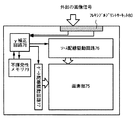
本実施例の電気光学装置は、絶縁基板上に形成されたTFTによって構成され、本願発明の不揮発性メモリの作製方法を用いることによって作製することができる。なお、液晶またはEL層の形成等のTFT形成後の工程については公知の方法を用いて作製すれば良い。
【0171】
図12は上記電気光学装置のブロック図である。画素部75の周辺にソース配線駆動回路76、ゲート配線駆動回路77が設けられ、さらにγ補正回路78、不揮発性メモリ79が設けられている。また、画像信号、クロック信号若しくは同期信号等は、FPC(フレキシブルプリントサーキット)80を経由して送られてくる。
【0172】
不揮発性メモリ79には、パソコン本体やテレビ受信アンテナ等から送られてきた画像信号にγ補正をかけるための補正データが格納(記憶)されており、その補正データを参照してγ補正回路78が画像信号に対してγ補正を行う。
【0173】
γ補正のためのデータは電気光学装置を出荷する前に一度格納しておけば良いが、定期的に補正データを書き換えることも可能である。また、同じように作成した電気光学装置であっても、微妙に液晶の光学応答特性(先の透過光強度と印加電圧の関係など)が異なる場合がある。その場合も、本実施例では電気光学装置毎に異なるγ補正データを格納しておくことが可能なので、常に同じ画質を得ることが可能である。
【0174】
なお、不揮発性メモリ79に対してγ補正の補正データを格納する際、本出願人による特願平10−156696号に記載された手段を用いることは好ましい。また、γ補正に関する説明も同出願になされている。
【0175】
また、不揮発性メモリに格納する補正データはデジタル信号であるので、必要に応じてD/Aコンバータ若しくはA/Dコンバータを同一基板上に形成することが望ましい。
【0176】
次に、本願発明の不揮発性メモリと、画素部と、画素部を駆動する駆動回路と、メモリコントローラ回路とを少なくとも有する電気光学装置の例を図13を用いて説明する。
【0177】
本実施例におけるメモリコントローラ回路とは不揮発性メモリに画像データを格納したり読み出したりという動作を制御するための制御回路である。
【0178】
なお、本実施例では、画素部を駆動する駆動回路として、ソース配線駆動回路およびゲート配線駆動回路をそれぞれ1つずつ設けているが、それぞれ複数の駆動回路を設けても構わない。また、画素部、画素部を駆動する駆動回路、およびメモリコントローラ回路については、公知の回路構造を用いれば良い。
【0179】
本実施例の電気光学装置は、絶縁基板上に形成されたTFTによって構成され、本願発明の不揮発性メモリの作製方法を用いることによって作製することができる。なお、液晶またはEL層の形成等のTFT形成後の工程については公知の方法を用いて作製すれば良い。
【0180】
図13は本実施例の電気光学装置のブロック図である。画素部81の周辺にソース配線駆動回路82、ゲート配線駆動回路83が設けられ、さらにメモリコントローラ回路84、本願発明の不揮発性メモリ85が設けられている。また、画像信号、クロック信号若しくは同期信号等は、FPC(フレキシブルプリントサーキット)86を経由して送られてくる。
【0181】
不揮発性メモリ85には、パソコン本体やテレビ受信アンテナ等から送られてきた画像信号が1フレーム毎に格納(記憶)されており、その画像信号を順次画素部に入力して表示を行う。不揮発性メモリ85には画素部81に表示される画像1フレーム分の画像情報が記憶される。例えば、6ビットのデジタル信号が画像信号として送られてくる場合、画素数×6ビットに相当するメモリ容量を必要とする。
【0182】
なお、不揮発性メモリに格納する補正データはデジタル信号であるので、必要に応じてD/Aコンバータ若しくはA/Dコンバータを同一基板上に形成することが望ましい。
【0183】
本実施例の構成とし、画素部81に表示された画像を常に不揮発性メモリ85に記憶することで、画像の一時停止などの動作を容易に行うことができる。即ち、メモリコントローラ回路84により不揮発性メモリ85に格納された画像信号を常に画素部81へ送るようにすることで、ビデオデッキ等に録画することなくテレビ放送を自由に一時停止することが可能となる。
【0184】
また、本実施例では1フレーム分を格納する例を示したが、さらに数百フレーム、数千フレーム分といった画像情報を格納しうる程度まで不揮発性メモリ85のメモリ容量を増やすことができたならば、一時停止だけでなく、数秒若しくは数分前の画像を再生(リプレイ)することも可能となる。
【0185】
なお、本実施例の構成は、実施例1〜7のいずれの構成とも自由に組み合わせて実施することができる。
【0186】
(実施例9)
本願発明の不揮発性メモリには、様々な用途がある。本実施例では、これらの不揮発性メモリを用いた電子機器について説明する。
【0187】
その様な電子機器としては、ビデオカメラ、デジタルカメラ、プロジェクター(リア型またはフロント型)、ヘッドマウントディスプレイ、ゴーグル型ディスプレイ、ゲーム機、カーナビゲーション、パーソナルコンピュータ、携帯情報端末(モバイルコンピュータ、携帯電話または電子書籍等)、DVDプレーヤーなどが挙げられる。それらの一例を図14、15に示す。
【0188】
図14(A)はディスプレイであり、筐体2001、支持台2002、表示部2003等を含む。本願発明の不揮発性メモリは、表示部2003やその他の信号制御回路と一体形成されてもよい。
【0189】
図14(B)はビデオカメラであり、本体2101、表示部2102、音声入力部2103、操作スイッチ2104、バッテリー2105、受像部2106で構成される。本願発明の不揮発性メモリは、表示部2102やその他の信号制御回路と一体形成されてもよい。
【0190】
図14(C)はヘッドマウントディスプレイの一部(右片側)であり、本体2201、信号ケーブル2202、頭部固定バンド2203、表示部2204、光学系2205、表示部2206等を含む。本願発明の不揮発性メモリは表示部2206やその他の信号制御回路と一体形成されてもよい。
【0191】
図14(D)は記録媒体を備えた画像再生装置(具体的にはDVD再生装置)であり、本体2301、記録媒体2302、操作スイッチ2303、表示部2304、2305等で構成される。なお、この装置は記録媒体としてDVD(Digital Versatile Disc)、CD等を用い、音楽鑑賞や映画鑑賞やゲームやインターネットを行うことができる。本願発明の不揮発性メモリは表示部2304やその他の信号制御回路と一体形成されてもよい。
【0192】
図14(E)はゴーグル型ディスプレイであり、本体2401、表示部2402、アーム部2403を含む。本願発明の不揮発性メモリは表示部2402やその他の信号制御回路と一体形成されてもよい。
【0193】
図14(F)はパーソナルコンピュータであり、本体2501、筐体2502、表示部2503、キーボード2504等で構成される。本願発明の不揮発性メモリは、表示部2503やその他の信号制御回路と一体形成されてもよい。
【0194】
図15(A)は携帯電話であり、本体2601、音声出力部2602、音声入力部2603、表示部2604、操作スイッチ2605、アンテナ2606を含む。本願発明の不揮発性メモリは表示部2604やその他の信号制御回路と一体形成されてもよい。
【0195】
図15(B)は音響再生装置、具体的にはカーオーディオであり、本体2701、表示部2702、操作スイッチ2703、2704を含む。本願発明の不揮発性メモリは表示部2702やその他の信号制御回路と一体形成されてもよい。また、本実施例では車載用オーディオを示すが、携帯型や家庭用の音響再生装置に用いても良い。
【0196】
以上の様に、本願発明の適用範囲は極めて広く、あらゆる分野の電子機器に適用することが可能である。また、本実施例の電子機器は実施例1〜8のどのような組み合わせからなる構成を用いても実現することができる。
【0197】
【発明の効果】
本願発明によると、不揮発性メモリが、その駆動回路および他の周辺回路と共に絶縁基板上に一体形成され、小型化を図ることができる。
【0198】
また、本願発明によると、不揮発性メモリを構成する各メモリセルにおいて、メモリTFTとスイッチングTFTが同一の半導体活性層上に形成されるため、不揮発性メモリの小型化を図ることができる。
【0199】
また、本願発明によると、不揮発性メモリの半導体活性層の膜厚が比較的薄いので、インパクトイオン化が起こりやすく、低電圧駆動でかつ劣化の少ない不揮発性メモリが実現される。
【0200】
さらに、本願発明の不揮発性メモリは、TFTで構成された任意の回路と絶縁基板上に一体形成することにより、不揮発性メモリを具備する半導体装置の小型化を図ることができる。
【図面の簡単な説明】
【図1】 本願発明の不揮発性メモリの回路構成を示す図。
【図2】 本願発明の不揮発性メモリを構成するメモリセルの断面図。
【図3】 実施例1の不揮発性メモリの作製工程を示す図。
【図4】 実施例1の不揮発性メモリの作製工程を示す図。
【図5】 実施例1の不揮発性メモリの作製工程を示す図。
【図6】 実施例1の不揮発性メモリの作製工程を示す図。
【図7】 本願発明の不揮発性メモリを構成するメモリセルの上面図。
【図8】 実施例4の不揮発性メモリを構成するメモリセルの回路図。
【図9】 実施例2の不揮発性メモリの作製工程を示す図。
【図10】 実施例2の不揮発性メモリの作製工程を示す図。
【図11】 実施例2の不揮発性メモリの作製工程を示す図。
【図12】 実施例8の不揮発性メモリを用いた電気光学装置。
【図13】 実施例8の不揮発性メモリを用いた電気光学装置。
【図14】 実施例9の不揮発性メモリを用いた電子機器。
【図15】 実施例9の不揮発性メモリを用いた電子機器。
【符号の説明】
101 Xアドレスデコーダ
102 Yアドレスデコーダ
103、104 周辺回路
201、202、203 ソース・ドレイン領域
204、205 チャネル形成領域
206 第1のゲート絶縁膜
207 ゲート絶縁膜
208 フローティングゲート電極
209 ゲート電極
210 第2のゲート絶縁膜
211 コントロールゲート電極
212 層間絶縁膜
213、214 ソース・ドレイン配線
215 コントロールゲート配線
Tr1 メモリTFT
Tr2 スイッチングTFT[0001]
[Technical field to which the invention belongs]
The present invention relates to a nonvolatile memory composed of thin film transistors (hereinafter referred to as TFTs) formed using SOI (Silicon On Insulator) technology and a method for manufacturing the same. In particular, the present invention relates to a nonvolatile memory, particularly an EEPROM (Electrically Erasable and Programmable Read Only Memory) integrally formed on a substrate having an insulating surface together with peripheral circuits such as a driving circuit. The present invention also relates to a semiconductor device including a nonvolatile memory integrally formed over a substrate having an insulating surface together with an arbitrary circuit formed of a thin film transistor (TFT).
[0002]
Note that in this specification, a semiconductor device refers to all devices that function by utilizing semiconductor characteristics, for example, an electro-optical device typified by a liquid crystal display device and an EL display device, and an electronic apparatus equipped with the electro-optical device. Is included in the category.
[0003]
[Prior art]
In recent years, semiconductor devices are rapidly becoming multifunctional, highly functional, and miniaturized, and accordingly, the frequency of memory use in various semiconductor devices is increasing. Against this background, high performance, high storage capacity, high reliability, and a small memory have been demanded.
[0004]
Currently, a semiconductor nonvolatile memory made of a magnetic disk or bulk silicon is most often used as a storage device of a semiconductor device.
[0005]
The magnetic disk is one of the largest storage capacities among the storage devices used in the semiconductor device, but has the disadvantages that it is difficult to reduce the size and the writing / reading speed is slow.
[0006]
On the other hand, the semiconductor nonvolatile memory is currently inferior to the magnetic disk in terms of storage capacity, but its writing / reading speed is several tens of times that of the magnetic disk. Semiconductor non-volatile memories have been developed that have sufficient performance with respect to the number of rewrites and data retention time. Against this background, there has recently been an increasing trend to use semiconductor memory as an alternative to magnetic disks.
[0007]
[Problems to be solved by the invention]
Since the conventional semiconductor nonvolatile memory is manufactured using bulk silicon and housed in a package, when such a semiconductor nonvolatile memory is mounted on a semiconductor device, the number of processes is increased and the package size is increased. In particular, this has hindered the miniaturization of semiconductor devices.
[0008]
The present invention has been made in view of the above circumstances, and an object of the present invention is to provide a non-volatile memory that can be integrally formed with components of other semiconductor devices and can be miniaturized. It is another object of the present invention to provide a semiconductor device including a nonvolatile memory that can be reduced in size.
[0009]
[Means for Solving the Problems]
As means for solving the above problems, in the present invention, the nonvolatile memory is configured by using a thin film transistor (TFT) formed by using SOI (Silicon On Insulator) technology.
[0010]
According to the present invention, the nonvolatile memory can be integrally formed on an insulating substrate together with an arbitrary circuit formed of a thin film transistor (TFT). In particular, it is possible to provide a non-volatile memory that can be reduced in size by integrally forming a memory cell, its drive circuit (typically, an address decoder) and other peripheral circuits on an insulating substrate. . Furthermore, it is possible to provide a semiconductor device including a non-volatile memory that can be reduced in size by being integrally formed on an insulating substrate together with an arbitrary circuit formed of TFTs that constitute another semiconductor device. It becomes.
[0011]
Specifically, the nonvolatile memory of the present invention has a memory cell array in which memory cells are arranged in a matrix, and each memory cell includes a memory TFT and a switching TFT. Further, it may include a memory cell driving circuit and other peripheral circuits.
[0012]
In the present invention, the memory TFTs constituting the memory cells and the semiconductor active layers of the switching TFTs are continuously connected. In other words, the memory TFT and the switching TFT included in each memory cell are formed on the same semiconductor active layer. By adopting such a structure, the memory cell area can be reduced as compared with the case where the memory TFT and the switching TFT constituting each memory cell are formed on separate semiconductor active layers.
[0013]
Further, the semiconductor active layer of the memory TFT is thinner than the semiconductor active layer of the switching TFT, or is formed to have a film thickness of 1 to 100 nm (preferably 1 to 50 nm, more preferably 10 to 40 nm). . Thus, by forming the semiconductor active layer of the memory TFT thinly, it becomes possible to write more efficiently than when the film thickness is large. This also means that writing with a lower driving voltage is possible, and at the same time, the structure can withstand a larger number of rewrites.
[0014]
The nonvolatile memory manufacturing process of the present invention includes a step of forming a first amorphous semiconductor layer and a second amorphous semiconductor layer on an insulating substrate, and these amorphous semiconductor layers. And crystallizing and forming a crystalline semiconductor layer comprising a region having a first thickness and a region having a second thickness.
[0015]
In the crystalline semiconductor layer thus formed, a memory TFT having a region having the first thickness as a semiconductor active layer is formed, and a switching TFT having a region having the second thickness as a semiconductor active layer is formed. By forming it, it becomes possible to manufacture a nonvolatile memory having memory cells in which the memory TFT and the semiconductor active layer of the switching TFT are continuously connected. Furthermore, by forming the first film thickness to be thinner than the second film thickness or to the first film thickness of 1 to 100 nm (preferably 1 to 50 nm, more preferably 10 to 40 nm), The nonvolatile memory of the present invention can be manufactured.
[0016]
The configuration of the present invention is shown below.
[0017]
A non-volatile memory including at least a memory cell array in which memory cells including memory TFTs and switching TFTs are arranged in a matrix,
The memory TFT includes at least a first semiconductor active layer formed on an insulating substrate, a first insulating film, a floating gate electrode, a second insulating film, and a control gate electrode,
The switching TFT includes at least a second semiconductor active layer formed on the insulating substrate, a gate insulating film, and a gate electrode,
The memory TFT and the switching TFT are integrally formed on the insulating substrate,
The first semiconductor active layer and the second semiconductor active layer are continuously connected,
A nonvolatile memory is provided in which the thickness of the first semiconductor active layer is thinner than the thickness of the second semiconductor active layer.
[0018]
The thickness of the first and second semiconductor active layers is preferably 1 to 150 nm.
[0019]
A nonvolatile memory in which memory cells including memory TFTs and switching TFTs are arranged in a matrix,
The memory TFT includes at least a first semiconductor active layer formed on an insulating substrate, a first insulating film, a floating gate electrode, a second insulating film, and a control gate electrode,
The switching TFT includes at least a second semiconductor active layer formed on the insulating substrate, a gate insulating film, and a gate electrode,
The memory TFT and the switching TFT are integrally formed on the insulating substrate,
The first semiconductor active layer and the second semiconductor active layer are continuously connected,
A nonvolatile memory is provided in which the thickness of the first semiconductor active layer is 1 to 100 nm, and the thickness of the second semiconductor active layer is 1 to 150 nm.
[0020]
Preferably, the first semiconductor active layer has a thickness of 1 to 50 nm, and the second semiconductor active layer has a thickness of 10 to 100 nm.
[0021]
More preferably, the thickness of the first semiconductor active layer is 10 to 40 nm.
[0022]
The first semiconductor active layer preferably has a thickness that is more likely to cause impact ionization than the second semiconductor active layer.
[0023]
The first tunnel current that flows between the floating gate electrode of the memory TFT and the first semiconductor active layer is the second tunnel current that flows between the gate electrode of the switching TFT and the second semiconductor active layer. It is preferably 2 times or more.
[0024]
The memory TFT and the switching TFT are preferably p-channel TFTs.
[0025]
There is provided a nonvolatile memory including at least a memory cell driving circuit, wherein the memory cell array and the memory cell driving circuit are integrally formed on the insulating substrate.
[0026]
A semiconductor device comprising at least a pixel circuit in which a plurality of pixel TFTs are arranged in a matrix on an insulating substrate, a drive circuit composed of TFTs for driving the plurality of pixel TFTs, and the nonvolatile memory. And
A semiconductor device is provided in which the pixel circuit, the driving circuit, and the nonvolatile memory are integrally formed on the insulating substrate.
[0027]
As the semiconductor device, a liquid crystal display device, an EL (electroluminescence) display device, or the like is provided. The EL display device is also called a light emitting device or a light emitting diode. The EL device of this specification also includes triplet and singlet light emitting devices.
[0028]
As the semiconductor device, a display, a video camera, a head mounted display, a DVD player, a goggle type display, a personal computer, a mobile phone, a car audio, and the like are provided.
[0029]
A non-volatile memory manufacturing method including at least a memory cell array in which memory cells each including a memory TFT and a switching TFT are arranged in a matrix,
Forming a first amorphous semiconductor layer and a second amorphous semiconductor layer on an insulating substrate;
A crystalline semiconductor layer comprising a region having a first thickness and a region having a second thickness by crystallizing the first amorphous semiconductor layer and the second amorphous semiconductor layer Forming a step;
A step of forming a memory TFT having a region having the first film thickness as a first semiconductor active layer in the crystalline semiconductor layer; and a region having the second film thickness as a second semiconductor active layer. Forming a switching TFT,
A method for producing a non-volatile memory including:
There is provided a method for manufacturing a nonvolatile memory, wherein the first film thickness is thinner than the second film thickness.
[0030]
In the method for manufacturing the nonvolatile memory, the first and second film thicknesses are preferably 1 to 150 nm.
[0031]
A non-volatile memory manufacturing method including at least a memory cell array in which memory cells each including a memory TFT and a switching TFT are arranged in a matrix,
Forming a first amorphous semiconductor layer and a second amorphous semiconductor layer on an insulating substrate;
A crystalline semiconductor layer comprising a region having a first thickness and a region having a second thickness by crystallizing the first amorphous semiconductor layer and the second amorphous semiconductor layer Forming a step;
Forming a memory TFT having a region having the first film thickness as a first semiconductor active layer in the crystalline semiconductor layer;
Forming a switching TFT having a region having the second film thickness as a second semiconductor active layer;
A method for producing a non-volatile memory including:
There is provided a method for manufacturing a nonvolatile memory, wherein the first film thickness is 1 to 100 nm, and the second film thickness is 1 to 150 nm.
[0032]
In the method for manufacturing a nonvolatile memory, it is preferable that the first film thickness is 1 to 50 nm and the second film thickness is 10 to 100 nm.
[0033]
In the method for manufacturing the nonvolatile memory, the first film thickness is more preferably 10 to 40 nm.
[0034]
In the method for manufacturing a nonvolatile memory, it is preferable that the first semiconductor active layer has a thickness that allows impact ionization to occur more easily than the second semiconductor active layer.
[0035]
In the non-volatile memory manufacturing method, the first tunnel current flowing between the floating gate electrode of the memory TFT and the first semiconductor active layer is generated between the gate electrode of the switching TFT and the second semiconductor active layer. It is preferably at least twice the second tunnel current flowing between them.
[0036]
In the method for manufacturing the nonvolatile memory, the memory TFT and the switching TFT are preferably p-channel TFTs.
[0037]
There is provided a method for manufacturing a nonvolatile memory, comprising at least a memory cell driving circuit, wherein the memory cell array and the memory cell driving circuit are integrally formed on the insulating substrate.
[0038]
A method for manufacturing a semiconductor device using a method for manufacturing a nonvolatile memory in the previous period,
The semiconductor device includes at least a pixel portion, a drive circuit that drives the pixel portion, and a nonvolatile memory manufactured by the method for manufacturing the nonvolatile memory,
There is provided a method for manufacturing a semiconductor device, wherein the pixel portion, the driver circuit, and the nonvolatile memory are formed over an insulating substrate.
[0039]
As a method for manufacturing the semiconductor device, a method for manufacturing a liquid crystal display device, an EL display device, or the like is provided.
[0040]
As a method for manufacturing the semiconductor device, a method for manufacturing a display, a video camera, a head mounted display, a DVD player, a goggle type display, a personal computer, a mobile phone, a car audio, or the like is provided.
[0041]
DETAILED DESCRIPTION OF THE INVENTION
Hereinafter, a circuit diagram of the nonvolatile memory of the present invention and a driving method thereof will be described in the case of m × n bits. In addition, an upper surface structure and a cross-sectional structure of a memory cell included in the nonvolatile memory will be described with examples.
[0042]
A method for manufacturing a nonvolatile memory according to the present invention will also be briefly described. A manufacturing method will be described in detail in Examples 1 and 2.
[0043]
Note that the nonvolatile memory in this embodiment is formed over an insulating substrate together with its driving circuit (in this embodiment, an address decoder) and other peripheral circuits, and in some cases, with other components of the semiconductor device. It is integrally formed. In this embodiment, an EEPROM (Electrically Erasable and Programmable Read Only Memory) is particularly described as a nonvolatile memory.
[0044]
FIG. 1 shows a circuit diagram of an m × n-bit nonvolatile memory according to the present invention. In the present embodiment, the m × n-bit nonvolatile memory includes a plurality of electrically erasable memory TFTs (memory elements, storage elements) Tr1, a plurality of switching TFTs Tr2, an X address decoder 101, a Y address decoder 102, and others. Peripheral circuits 103 and 104. Other peripheral circuits include an address buffer circuit and a control logic circuit, and are provided as necessary. The memory TFT Tr1 is a TFT having a floating gate, and records 1-bit data. In the present invention, the memory TFT Tr1 and the switching TFT Tr2 need to be the same conductivity type TFT. Note that the memory TFT Tr1 and the switching TFT Tr2 may be either n-channel or p-channel type TFTs, but are preferably p-channel TFTs.
[0045]
The source electrode of the memory TFT Tr1 and the drain electrode of the switching TFT Tr2 are electrically connected, and a 1-bit memory cell is constituted by a series connection circuit of these two TFTs. In this embodiment, the memory cells are arranged in a matrix of m vertical × n horizontal (m and n are integers of 1 or more, respectively). Since each memory cell can store 1-bit information, the nonvolatile memory of this embodiment has a storage capacity of m × n bits.
[0046]
As shown in FIG. 1, the memory cells constituting the m × n-bit nonvolatile memory are denoted by (1, 1), (2, 1) to (n, m). The memory cells arranged in each column are connected at both ends to signal lines labeled A1, B1 to An, Bn, and the memory cells arranged in each row have a signal. Lines C1, D1 to Cm, and Dm are connected. Specifically, the signal line Ai is connected to the drain electrode of the memory TFT Tr1 included in each of the memory cells (i, 1), (i, 2) to (i, m) arranged in the i-th column, and switching is performed. A signal line Bi is connected to the source electrode of the TFT (i is an integer from 1 to n). Further, the signal line Cj is connected to the control gate electrode of the memory TFT Tr1 included in the memory cells (1, j), (2, j) to (n, j) arranged in the jth row, and the gate of the switching TFT Tr2. A signal line Dj is connected to the electrode (j is an integer from 1 to m).
[0047]
The signal lines A1, B1 to An, Bn, and C1, D1 to Cm, and Dm are connected to the X address decoder 101 and the Y address decoder 102, respectively. A specific memory cell is designated by the X address decoder 101 and the Y address decoder 102, and data is written, read, and erased.
[0048]
Here, the operation of the nonvolatile memory according to the present embodiment will be described using the memory cell (1, 1) in FIG. 1 as an example.
[0049]
First, when data is written to the memory TFT Tr1, the switching TFT Tr2 is turned on via the signal line D1. Further, an appropriate potential difference is applied between the drain electrode of the memory TFT Tr1 and the source electrode of the switching TFT Tr2 via the signal lines A1 and B1. When a positive high voltage (for example, 20 V) is applied to the memory TFT Tr1 control gate via the signal line C1, carriers (in this case, holes) moving in the channel formation region of the memory TFT Tr1 are accelerated, and weak avalanche collapse or impact ionization is performed. And a number of high energy electrons (hot electrons) are generated. Then, hot electrons get over the energy barrier of the gate insulating film and are injected into the floating gate electrode. In this way, charges are accumulated in the floating gate electrode and writing is performed. The threshold voltage of the memory TFT Tr1 changes depending on the amount of charge accumulated in the floating gate electrode.
[0050]
When reading data from the memory cell, for example, the switching TFT Tr2 is turned on via the signal line D1, 0V is applied to the control gate of the memory TFT Tr1 via the signal line C1, and the switching TFT Tr2 is established via the signal line B1. You should put the source of this in GND. As a result, the conduction or non-conduction of the memory TFT Tr1 is determined according to the charge accumulated in the floating gate electrode of the memory TFT Tr1, and the data stored in the memory cell is read from the signal line A1.
[0051]
Next, when erasing data stored in the memory TFT Tr1, the switching TFT Tr2 is turned on via the signal line D1, and the source electrode of the switching TFT TR1 is set to GND via the signal line B1. When a negative high voltage (for example, −20 V) is applied to the signal line C1, electrons trapped in the floating gate electrode are emitted to the drain region by a tunnel current. As a result, the stored data is erased.
[0052]
Table 1 shows specific examples of voltages applied to the signal lines A1, B1, C1, and D1 based on the above-described operation. Note that both the memory TFT Tr1 and the switching TFT Tr2 are p-channel TFTs.
[0053]
[Table 1]
The voltage applied to the signal line shown in Table 1 is an example, and is not limited to the values in Table 1. For example, the voltage applied to the memory TFT depends on the thickness of the semiconductor active layer of the memory TFT, the capacitance between the control gate electrode and the floating gate electrode, and the like. The operating voltage of the memory TFT also changes accordingly.
[0055]
Further, the memory TFT Tr1 and the switching TFT Tr2 may be n-channel TFTs. In that case, for example, all voltages applied to the signal line D1 may be + 5V. Note that when an n-channel TFT is used as the memory TFT, a larger current flows at the time of writing than in the case where a p-channel TFT is used, and deterioration may be quick. Therefore, in the present embodiment, the memory TFT Tr1 is preferably a p-channel type.
[0056]
In this embodiment, when writing / erasing the memory TFT, a voltage of + 20 / -20 V is not applied to the control gate electrode of the memory TFT at a time, but a voltage lower than this voltage is applied several times. You may apply with a pulse. In this case, deterioration of the TFT can be suppressed to some extent.
[0057]
Next, a top structure and a cross-sectional structure of a memory cell constituting the nonvolatile memory of the present invention will be described with reference to FIGS.
[0058]
First, an example of a top view of a memory cell constituting the nonvolatile memory of the present invention is shown. FIG. 7 shows a top view of a region including four memory cells (1, 1), (1, 2), (2, 1), (2, 2) (see FIG. 1).
[0059]
In FIG. 7,
[0060]
Next, a cross-sectional view of a memory cell constituting the nonvolatile memory of the present invention is shown. FIG. 2 shows a cross-sectional structure of the memory cell shown in FIG. 7 (for example, a cross-sectional structure of AA ′ in the memory cells (1, 2)).
[0061]
In FIG. 2, the left TFT is the memory TFT Tr1, and the right TFT is the switching TFT Tr2. The semiconductor active layer forming the memory TFT Tr1 and the switching TFT Tr2 includes source /
[0062]
As shown in FIG. 2 (and FIG. 7), in the present invention, the semiconductor active layer of the memory TFT Tr1 and the semiconductor active layer of the switching TFT Tr2 are directly connected. In other words, the source region of the memory TFT Tr1 and the drain region of the switching TFT Tr2 are electrically connected by sharing the semiconductor active layer. With such a structure, the area of the memory cell can be greatly reduced as compared with the case where the memory TFT Tr1 and the switching TFT Tr2 are formed on separate semiconductor active layers. A semiconductor device including a nonvolatile memory can be miniaturized.
[0063]
As shown in FIG. 2, the semiconductor active layer (thickness d1) of the memory TFT Tr1 is formed thinner than the semiconductor active layer (thickness d2) of the switching TFT Tr2. That is, d1 <d2 holds. With such a structure, impact ionization (impact ionization, impact ionization, or impact ionization) is more likely to occur in the semiconductor active layer of the memory TFT Tr1, and as a result, charge to the floating gate electrode of the memory TFT Tr1 is reduced. Injection tends to occur. Note that the thicknesses of the semiconductor active layers of the TFTs constituting the X address decoder 101, the Y address decoder 102, and other peripheral circuits may be the same as the thickness d2 of the switching TFT Tr2.
[0064]
Further, the
[0065]
In addition to this embodiment, Example 2 can be referred to for an example of a cross-sectional structure of the memory cell. Thus, in the present invention, the semiconductor active layer of the memory TFT Tr1 is thinner than the semiconductor active layers of the TFTs and switching TFTs constituting the address decoder and other peripheral circuits, or has a film thickness of 1 to 100 nm (preferably 1 To 50 nm, more preferably 10 to 40 nm).
[0066]
In the nonvolatile memory, the rewritable number of times and the information holding time are important. In order to improve the number of rewritable times, it is required to reduce the voltage applied to the control gate electrode of the memory TFT. In the nonvolatile memory of the present invention, as described above, since the semiconductor active layer of the memory TFT is formed thin, impact ionization easily occurs, and writing and erasing of the memory TFT can be performed at a low voltage. This is because the conventional non-volatile memory made of bulk silicon has a relatively thin gate insulating film, which causes deterioration of the gate insulating film, or the temperature of carriers accumulated in the floating gate electrode is low. It is an innovative solution to the spill of rising.
[0067]
Next, a method for manufacturing the nonvolatile memory of the present invention will be briefly described. Note that Example 1 and Example 2 can be referred to for a detailed manufacturing method.
[0068]
First, after forming and patterning a first amorphous semiconductor layer on an insulating substrate, a second amorphous semiconductor layer is formed. Then, the two amorphous semiconductor layers are crystallized to form a crystalline semiconductor layer including a region having a first thickness and a region having a second thickness. When the driver circuit for the memory cell and other peripheral circuits are formed integrally on the insulating substrate, a crystalline semiconductor layer having a second thickness is formed in that region.
[0069]
Note that in this specification, an amorphous semiconductor film refers to an entire semiconductor film including an amorphous structure, and includes a so-called amorphous semiconductor film and a microcrystalline semiconductor film. Further, a compound semiconductor film including an amorphous structure such as an amorphous silicon germanium film may be used.
[0070]
In this specification, a crystalline semiconductor layer refers to an entire semiconductor layer including a crystal structure, and includes a so-called single crystal semiconductor film and a polycrystalline semiconductor film. In addition, a semiconductor film (see Example 1) having a crystal structure in which rod-like crystals are gathered and produced by the technique described in Japanese Patent Laid-Open No. 10-247735 is included as a polycrystalline semiconductor film having particularly excellent crystallinity.
[0071]
Thereafter, by forming a memory TFT having a region having the first film thickness as a semiconductor active layer and a switching TFT having a region having the second film thickness as a semiconductor active layer, the semiconductor activity of the memory TFT and the switching TFT is formed. A nonvolatile memory having memory cells in which layers are continuously connected can be manufactured. Further, by simultaneously forming a CMOS circuit in which the crystalline semiconductor layer having the second film thickness is a semiconductor active layer, it is possible to integrally form a drive circuit for a memory cell and other peripheral circuits.
[0072]
Of course, the first film thickness and the second film thickness can be freely set within the range allowed by the apparatus, and the first film thickness is smaller than the second film thickness, or the first film thickness The non-volatile memory of the present invention can be manufactured by forming the film thickness of 1 to 100 nm (preferably 1 to 50 nm, more preferably 10 to 40 nm).
[0073]
By the above method for manufacturing a nonvolatile memory, the nonvolatile memory of the present invention can be formed integrally with any part of a semiconductor device that can be manufactured using thin film technology.
[0074]
In addition, when the manufacturing method described in
[0075]
【Example】
Example 1
In this embodiment, a method for manufacturing a nonvolatile memory using the present invention will be described with reference to FIGS. 3 to 6, as the TFTs constituting the nonvolatile memory of this embodiment, the memory TFT (p-channel TFT) and the switching TFT (p-channel TFT) constituting the memory cell, the address decoder, Description will be made by taking two TFTs (p-channel TFT and n-channel TFT) constituting a typical CMOS circuit as an example of other peripheral circuit.
[0076]
Further, according to the method for manufacturing a nonvolatile memory described below, it is understood that the nonvolatile memory of the present invention can be integrally formed with any part of a semiconductor device that can be manufactured using a thin film technology.
[0077]
In order to realize a non-volatile memory and a semiconductor device having a circuit composed of a memory cell, an address decoder and other TFTs on the same insulating substrate, a TFT having high characteristics in mobility, threshold voltage, etc. Is required. In particular, a TFT provided with a semiconductor active layer of amorphous silicon, which is often used conventionally, is not sufficient. According to the following manufacturing method, a TFT with high characteristics can be manufactured, and the nonvolatile memory and the semiconductor device of the present invention can be realized.
[0078]
Please refer to FIG. First, a quartz substrate 301 is prepared as a substrate having an insulating surface. A silicon substrate on which a thermal oxide film is formed can be used instead of the quartz substrate. Alternatively, a method may be employed in which an amorphous silicon film is once formed on a quartz substrate and is completely thermally oxidized to form an insulating film. Further, a quartz substrate or a ceramic substrate on which a silicon nitride film is formed as an insulating film may be used.
[0079]
Next, an amorphous silicon film 302 having a thickness of 25 nm is formed by a known film formation method (FIG. 3A). Note that it is not necessary to limit the amorphous silicon film, and any amorphous semiconductor film (including a microcrystalline semiconductor film and a compound semiconductor film including an amorphous structure such as an amorphous silicon germanium film) may be used. .
[0080]
Next, a resist film is formed and patterned to form a mask 311 (FIG. 3B). After that, the amorphous silicon film 302 is etched to form an amorphous silicon film 321 partially formed on the substrate (FIG. 3C). Note that the amorphous silicon film 321 may be etched by either dry etching or wet etching. In the case of dry etching, for example, CF Four + O 2 In the case of wet etching, an etching solution such as fluorine acid + nitric acid is preferably used.
[0081]
Next, an amorphous silicon film is again formed to a thickness of 50 nm by the method described above, and amorphous silicon films 331 and 332 as shown in FIG. 3D are formed. Here, the final film thickness was adjusted to 50 nm for the amorphous silicon film 331 and 75 nm for the amorphous silicon film 332. Note that the amorphous silicon film is not limited to the amorphous silicon film (including a microcrystalline semiconductor film and a compound semiconductor film including an amorphous structure such as an amorphous silicon germanium film). It ’s fine.
[0082]
Note that it is desirable to clean the surfaces of the amorphous silicon film 321 and the quartz substrate 301 before the second formation of the amorphous silicon film.
[0083]
Another method may be used for forming the amorphous silicon films 331 and 332. For example, an amorphous silicon film can be obtained by forming an amorphous silicon film as a whole to 75 nm by the above-described method, partially forming a mask, and partially reducing the film thickness by the above-described etching. .
[0084]
The amorphous silicon film 331 later becomes a semiconductor active layer of the memory TFT, and the amorphous silicon film 332 later becomes a semiconductor active layer such as a switching TFT and a peripheral CMOS circuit.
[0085]
When the final semiconductor active layer has a thickness of 150 nm or more, particularly 200 nm or more, the impact ionization peculiar to SOI is very little, which is almost the same as the case of non-volatile memory using bulk silicon. End up. Therefore, the characteristics of the nonvolatile memory based on the SOI technology cannot be extracted. Therefore, in the present invention, the final thickness of the semiconductor active layer is preferably 1 to 150 nm.
[0086]
In the present embodiment, as described above, the final film thickness of the amorphous silicon film 331 of the memory TFT is 50 nm, and the final film thickness of the amorphous silicon film 332 such as the switching TFT and the peripheral CMOS circuit. However, the film thickness may be set to 1 to 100 nm (preferably 1 to 50 nm, more preferably 10 to 40 nm) and 1 to 150 nm (preferably 10 to 100 nm). It is not limited.
[0087]
Next, a crystallization process of the amorphous silicon films 331 and 332 is performed. The process from here to FIG. 4 (B) can be completely cited in Japanese Patent Application Laid-Open No. 10-247735 by the present applicant. This publication discloses a technique related to a method for crystallizing a semiconductor film using an element such as Ni as a catalyst.
[0088]
First,
[0089]
In addition to nickel, the catalytic element is cobalt (Co), iron (Fe), palladium (Pd), platinum (Pt), copper (Cu), gold (Au), germanium (Ge), lead (Pb). Indium (In) or the like can be used.
[0090]
The catalyst element addition step is not limited to the spin coating method, and an ion implantation method using a resist mask, a plasma doping method, or a sputtering method can also be used. In this case, since the occupied area of the added region can be reduced and the crystal growth distance can be easily controlled, this is an effective technique for configuring a miniaturized circuit.
[0091]
Next, as shown in FIG. 4B, heat treatment is performed at 570 ° C. for 14 hours in an inert atmosphere to crystallize the amorphous silicon films 331 and 332. At this time, the
[0092]
Next, as shown in FIG. 4C, an element belonging to Group 15 (preferably phosphorus) is added to the Ni-added
[0093]
Next, as shown in FIG. 4C, heat treatment is performed in an inert atmosphere at 600 ° C. for 12 hours. By this heat treatment, Ni existing in the
[0094]
The concentration of Ni remaining in the
[0095]
Thus, a
[0096]
Next, in the island-shaped semiconductor
[0097]
As a result, a
[0098]
After that, the resist
[0099]
Next, heat treatment is performed in an oxidizing atmosphere at 950 ° C. for 1 hour to perform a thermal oxidation process. Note that the oxidizing atmosphere may be an oxygen atmosphere or an oxygen atmosphere to which a halogen element is added. In this thermal oxidation process, oxidation proceeds at the interface between the active layer and the silicon nitride oxide film, and the thickness of the
[0100]
Next, a conductive film with a thickness of 200 to 400 nm is formed and patterned to form
[0101]
Note that although the gate electrode may be formed of a single-layer conductive film, it is preferably a stacked film of two layers or three layers as necessary. A known conductive film can be used as the material of the gate electrode. Specifically, a film made of an element selected from tantalum (Ta), titanium (Ti), molybdenum (Mo), tungsten (W), chromium (Cr), and silicon (Si), or a nitride of the element. A film (typically a tantalum nitride film, a tungsten nitride film, a titanium nitride film), an alloy film (typically a Mo—W alloy or a Mo—Ta alloy), or a silicide film of the element. (Typically, a tungsten silicide film or a titanium silicide film) can be used.
[0102]
In this embodiment, a stacked film including a tungsten nitride (WN) film having a thickness of 50 nm and a tungsten (W) film having a thickness of 350 nm is used. This may be formed by sputtering. Further, when an inert gas such as xenon (Xe) or neon (Ne) is added as a sputtering gas, peeling of the film due to stress can be prevented.
[0103]
Next, an impurity element adding step for imparting one conductivity is performed. As the impurity element, phosphorus (P) or arsenic (As) may be used for n-type, and boron (B), gallium (Ga), indium (In), or the like may be used for p-type.
[0104]
First, as shown in FIG. 5D, an n-type impurity element (phosphorus in this embodiment) is added in a self-aligning manner using the
[0105]
Next, the
[0106]
Next, as shown in FIG. 6A, resist
[0107]
By this step, source /
[0108]
Next, as shown in FIG. 6B, the resist
[0109]
Thus, source /
[0110]
Next, as shown in FIG. 6C, after the resist
[0111]
Thereafter, the n-type or p-type impurity element added at each concentration is activated. As the activation means, furnace annealing, laser annealing, lamp annealing or the like may be combined. In this embodiment, heat treatment is performed in an electric furnace in a nitrogen atmosphere at 550 ° C. for 4 hours. At this time, damage to the active layer received in the addition process is also repaired. As the activation means, a furnace annealing method is preferable.
[0112]
Next, a conductive film having a thickness of 200 to 400 nm is formed and patterned to form a control gate electrode 622 (FIG. 6C). The
[0113]
Note that the control gate electrode may be formed of a single-layer conductive film, but is preferably a stacked film of two layers or three layers as necessary. A known conductive film can be used as the material of the gate electrode. Specifically, a film made of an element selected from tantalum (Ta), titanium (Ti), molybdenum (Mo), tungsten (W), chromium (Cr), and silicon (Si), or a nitride of the element. Or an alloy film in which the above elements are combined, or a silicide film of the above elements.
[0114]
In this embodiment, a laminated film including a tungsten nitride (WN) film having a thickness of 50 nm and a tungsten (W) film having a thickness of 350 nm is formed by a sputtering method. When an inert gas such as xenon (Xe) or neon (Ne) is added as a sputtering gas, film peeling due to stress can be prevented.
[0115]
Next, an
[0116]
Next, as shown in FIG. 6D, contact holes are formed in the
[0117]
Finally, hydrogenation is performed by heat treatment at 300 to 450 ° C. for 1 to 12 hours in an atmosphere containing 3 to 100% hydrogen. This step is a step in which the dangling bonds of the semiconductor film are terminated with hydrogen by thermally excited hydrogen. In this embodiment, hydrogenation is performed by performing heat treatment for 2 hours in a hydrogen atmosphere at 350 ° C. Further, as another means of hydrogenation, plasma hydrogenation (using hydrogen excited by plasma) may be performed. Further, the hydrogenation treatment may be performed before the contact hole is formed.
[0118]
Through the above steps, a TFT having a structure as shown in FIG. 6D can be manufactured.
[0119]
(Example 2)
In this embodiment, the case where a non-volatile memory is formed by inverted staggered TFTs will be described with reference to FIGS. 9 to 11 show, as TFTs constituting the nonvolatile memory of this embodiment, a memory TFT (p-channel TFT) and a switching TFT (p-channel TFT) constituting a memory cell, an address decoder, Description will be made by taking two TFTs (p-channel TFT and n-channel TFT) constituting a typical CMOS circuit as an example of other peripheral circuit.
[0120]
Please refer to FIG. First, a
[0121]
Next, a
[0122]
The gate insulating film on the memory TFT side defines the capacitance between the floating gate electrode and the control gate electrode to be formed in the next step, and is applied to the floating gate electrode by changing the film thickness. The voltage can be adjusted. Therefore, the thickness of the
[0123]
Next, a floating
[0124]
Next, an insulating
[0125]
Next,
[0126]
Further, it is not necessary to limit to an amorphous silicon film, and any amorphous semiconductor film (including a compound semiconductor film including an amorphous structure such as a microcrystalline semiconductor film and an amorphous silicon germanium film) may be used. .
[0127]
Next, the
[0128]
As strong light having the same intensity as laser light, strong light from a halogen lamp or a metal halide lamp, or strong light from an infrared light or ultraviolet light lamp can be used.
[0129]
In this embodiment, excimer laser light processed into a linear shape is scanned from one end to the other end of the substrate to crystallize the entire surface of the amorphous silicon film. At this time, the sweep speed of the laser beam is 1.2 mm / s, the processing temperature is room temperature, the pulse frequency is 30 Hz, and the laser energy is 300 to 315 mJ / cm. 2 And A crystalline silicon film is obtained by this process.
[0130]
Note that the crystallization method used in
[0131]
Reference is now made to FIG. First, the crystalline silicon film is patterned to form
[0132]
Next, an impurity element imparting one conductivity is added. As the impurity element, phosphorus (P) or arsenic (As) may be used for n-type, and boron (B), gallium (Ga), indium (In), or the like may be used for p-type.
[0133]
First, resist
[0134]
Next, the resist
[0135]
Next, the resist
[0136]
Next, after removing the resist
[0137]
After the laser annealing is finished, an
[0138]
Next, contact holes are formed in the
[0139]
Finally, the whole is subjected to heat treatment at 350 ° C. for about 2 hours in a hydrogen atmosphere, and the dangling bonds in the film (particularly the channel formation region) are terminated with hydrogen. Through the above steps, a TFT having a structure as shown in FIG. 11B can be manufactured.
[0140]
(Example 3)
In the cross-sectional view of the memory cell shown in FIG. 2, the semiconductor active layer (thickness d1) of the memory TFT is thinner than the semiconductor active layer (thickness d2) of the switching TFT, but d1 is 1 to 100 nm ( (Preferably 1 to 50 nm, more preferably 10 to 40 nm) and d2 may be formed in the range of 1 to 150 nm (preferably 10 to 100 nm). In particular, the semiconductor active layer of the memory TFT and the semiconductor active layer of the switching TFT may have the same thickness.
[0141]
Even if the semiconductor active layer of the TFT constituting the drive circuit of the memory cell and other peripheral circuits is formed to the same thickness as the semiconductor active layer of the memory TFT, the drive frequency of the memory TFT is not reduced within a range. It may be formed thicker than the semiconductor active layer.
[0142]
In this embodiment, the manufacturing methods of
[0143]
Example 4
In this embodiment, an example different from the circuit diagram of the memory cell in the nonvolatile memory shown in FIG. 1 will be described with reference to FIG. FIG. 8 is a circuit diagram of adjacent memory cells arranged in the same row in a memory cell array in which memory cells are arranged in a matrix. In FIG. 8, two adjacent memory cells share a signal line (referred to as signal line B) connected to the source electrode of the switching TFT.
[0144]
Specifically, the signal lines A and A ′ are connected to the drain electrodes of the left and right memory TFTs Tr1 and Tr1 ′, respectively, and the signal line B is connected to the source electrodes of the switching TFTs Tr2 and Tr2 ′. The signal line C is connected to the control gate electrodes of the memory TFTs Tr1 and Tr1 ′, and the signal line D is connected to the gate electrodes of the switching TFTs Tr2 and Tr2 ′. In the two memory cells, the memory TFT and the switching TFT are provided symmetrically with respect to the signal line B.
[0145]
By adopting such a structure, the number of signal lines B can be reduced as compared with the configuration shown in FIG. 1, and memory cells can be arranged at a higher density. As a result, the nonvolatile memory can be reduced in size or increased in capacity.
[0146]
In addition, a present Example can be combined with any structure of Examples 1-3.
[0147]
(Example 5)
In this embodiment, an inexpensive low-grade quartz substrate is first prepared. Next, the quartz substrate is polished to an ideal state (average value of the uneven portion difference is within 5 nm, typically within 3 nm, preferably within 2 nm) by a technique such as CMP (Chemical Mechanical Polishing).
[0148]
Thus, even an inexpensive quartz substrate can be used as an insulating substrate having excellent flatness by polishing. When a quartz substrate is used, the substrate becomes very dense and the stability of the substrate / semiconductor thin film interface is high. Further, since there is almost no influence of contamination from the substrate, the utility value is very high.
[0149]
In addition, a present Example can be combined with any structure of Examples 1-4.
[0150]
(Example 6)
In Examples 1 and 2, an example in which an element belonging to Group 15 (phosphorus in Examples 1 and 2) is used in the process of gettering the catalytic element that promotes crystallization of silicon has been described. In the present invention, it is also possible to use a halogen element in the catalyst element gettering step.
[0151]
In this embodiment, a catalytic element gettering step is performed by using a treatment atmosphere containing a halogen element in the heat treatment after the gate insulating film is formed over the semiconductor active layer (see FIG. 5A). .
[0152]
Note that the heat treatment is preferably performed at a temperature higher than 700 ° C. in order to obtain a sufficient gettering effect by the halogen element. Below this temperature, decomposition of the halogen compound in the processing atmosphere becomes difficult, and the gettering effect may not be obtained. Therefore, the heat treatment temperature is preferably 800 to 1000 ° C. (typically 950 ° C.), and the treatment time is 0.1 to 6 hours, typically 0.5 to 1 hour.
[0153]
As a typical example, in an atmosphere containing hydrogen chloride (HCl) at a concentration of 0.5 to 10% by volume (in this example, 3% by volume) with respect to an oxygen atmosphere, 950 ° C., 30 minutes. The heat treatment may be performed. If the HCl concentration is equal to or higher than the above concentration, the surface of the semiconductor active layer is not preferable because unevenness of about the film thickness occurs.
[0154]
In addition, as a compound containing a halogen element, HF and NF can be used in addition to HCl gas. Three , HBr, Cl 2 , ClF Three , BCl Three , F 2 , Br 2 One or a plurality of compounds selected from compounds containing a halogen element such as the above can be used.
[0155]
In this step, nickel in the semiconductor active layer is gettered by the action of chlorine, and becomes volatile nickel chloride which is released into the atmosphere and removed. And by this process, the concentration of nickel in the semiconductor active layer is 5 × 10 5. 17 atoms / cm Three The following (typically 2 × 10 17 atoms / cm Three Or less). According to the experiences of the present inventors, the nickel concentration is 1 × 10 18 atoms / cm Three Below (preferably 5 × 10 17 atoms / cm Three If the following), TFT characteristics are not adversely affected.
[0156]
The gettering process is also effective for metal elements other than nickel. The metal elements that can be mixed into the silicon film are mainly constituent elements of the film formation chamber (typically aluminum, iron, chromium, etc.). If the gettering process is performed, the concentration of these metal elements is considered. 5 × 10 17 atoms / cm Three The following (preferably 2 × 10 17 atoms / cm Three The following is possible:
[0157]
When the gettering process is performed, 1 × 10 6 halogen elements used for the gettering process are present in the semiconductor active layer. 16 ~ 1x10 20 atoms / cm Three Remain at a concentration of
[0158]
In addition, a thermal oxidation reaction proceeds at the interface between the semiconductor active layer and the gate insulating film by the heat treatment, and the thickness of the gate insulating film increases by the thermal oxide film. When the thermal oxide film is formed in this way, a semiconductor / insulating film interface with very few interface states can be obtained. In addition, there is an effect of preventing formation defects (edge thinning) of the thermal oxide film at the end portion of the active layer.
[0159]
As described above, the catalyst element gettering step using the halogen element is performed. Note that the other steps may be performed in accordance with the manufacturing steps shown in Example 1 or Example 2. As a result, a non-volatile memory having the same characteristics as those of Example 1 or Example 2 is obtained.
[0160]
In addition, a present Example can be combined with any structure of Examples 3-5.
[0161]
(Example 7)
In this example, in the manufacturing method described in Example 1 or Example 2, tantalum (Ta) or a Ta alloy is used for the gate electrode, and Ta is used as an insulating film between the floating gate electrode and the control gate electrode of the memory TFT. A case where a thermal oxide film of a gate electrode made of a Ta alloy is used will be described.
[0162]
In the case of the manufacturing method described in
[0163]
When Ta or Ta alloy is used for the gate electrode, it can be thermally oxidized at about 450 ° C. to about 600 ° C. 2 O Three An oxide film having a good quality such as a film is formed on the gate electrode.
[0164]
The dielectric constant of the insulating film thus formed is, for example, Ta 2 O Three In this case, the capacitance is approximately 11.6, which is larger than that of the insulating film containing silicon. When the same film thickness is used, a larger capacitance is formed between the floating gate and the control gate. As a result, by using a thermal oxide film of Ta or Ta alloy, it is possible to manufacture a nonvolatile memory having a structure in which charges are easily injected into the floating gate as compared with an insulating film containing silicon.
[0165]
In addition, this embodiment can be combined with any of the configurations of Embodiments 3 to 6.
[0166]
(Example 8)
The nonvolatile memory of the present invention has various uses. In this embodiment, an electro-optical device (typically, a liquid crystal display device and an EL display device) including the nonvolatile memory of the present invention as a memory portion will be described.
[0167]
First, an example of an electro-optical device having at least a nonvolatile memory according to the present invention, a pixel portion, a drive circuit for driving the pixel portion, and a γ (gamma) correction circuit will be described with reference to FIG.
[0168]
The γ correction circuit is a circuit for performing γ correction. The γ correction is a correction for creating a linear relationship between the voltage applied to the pixel electrode and the transmitted light intensity of the liquid crystal or EL layer thereon by applying an appropriate voltage to the image signal.
[0169]
In this embodiment, one source wiring driving circuit and one gate wiring driving circuit are provided as driving circuits for driving the pixel portion, but a plurality of driving circuits may be provided. A known circuit structure may be used for the pixel portion, the drive circuit that drives the pixel portion, and the γ (gamma) correction circuit.
[0170]
The electro-optical device of this embodiment is constituted by TFTs formed on an insulating substrate, and can be manufactured by using the method for manufacturing a nonvolatile memory of the present invention. In addition, what is necessary is just to produce about the process after TFT formation, such as formation of a liquid crystal or an EL layer, using a well-known method.
[0171]
FIG. 12 is a block diagram of the electro-optical device. A source wiring driving circuit 76 and a gate wiring driving circuit 77 are provided around the pixel portion 75, and a γ correction circuit 78 and a nonvolatile memory 79 are further provided. An image signal, a clock signal, a synchronization signal, or the like is sent via an FPC (flexible printed circuit) 80.
[0172]
The nonvolatile memory 79 stores (stores) correction data for applying γ correction to an image signal transmitted from a personal computer main body, a television receiving antenna, or the like. The γ correction circuit 78 is referred to the correction data. Performs γ correction on the image signal.
[0173]
Data for γ correction may be stored once before the electro-optical device is shipped, but the correction data can be rewritten periodically. Further, even an electro-optical device produced in the same way may have slightly different optical response characteristics (such as the relationship between the transmitted light intensity and the applied voltage). Also in this case, in this embodiment, different γ correction data can be stored for each electro-optical device, so that the same image quality can always be obtained.
[0174]
When storing correction data for γ correction in the non-volatile memory 79, it is preferable to use the means described in Japanese Patent Application No. 10-156696 by the present applicant. Further, the application regarding the γ correction is also made in the same application.
[0175]
Since the correction data stored in the nonvolatile memory is a digital signal, it is desirable to form a D / A converter or an A / D converter on the same substrate as necessary.
[0176]
Next, an example of an electro-optical device including at least a nonvolatile memory according to the present invention, a pixel portion, a driving circuit for driving the pixel portion, and a memory controller circuit will be described with reference to FIG.
[0177]
The memory controller circuit in this embodiment is a control circuit for controlling operations such as storing and reading image data in a nonvolatile memory.
[0178]
In this embodiment, one source wiring driving circuit and one gate wiring driving circuit are provided as driving circuits for driving the pixel portion, but a plurality of driving circuits may be provided. A known circuit structure may be used for the pixel portion, the driver circuit that drives the pixel portion, and the memory controller circuit.
[0179]
The electro-optical device of this embodiment is constituted by TFTs formed on an insulating substrate, and can be manufactured by using the method for manufacturing a nonvolatile memory of the present invention. In addition, what is necessary is just to produce about the process after TFT formation, such as formation of a liquid crystal or an EL layer, using a well-known method.
[0180]
FIG. 13 is a block diagram of the electro-optical device of this embodiment. A source wiring driving circuit 82 and a gate wiring driving circuit 83 are provided around the pixel portion 81, and a memory controller circuit 84 and a nonvolatile memory 85 of the present invention are also provided. An image signal, a clock signal, a synchronization signal, or the like is sent via an FPC (flexible printed circuit) 86.
[0181]
The nonvolatile memory 85 stores (stores) image signals sent from a personal computer main body, a television receiving antenna or the like for each frame, and sequentially inputs the image signals to the pixel portion for display. The nonvolatile memory 85 stores image information for one frame displayed on the pixel unit 81. For example, when a 6-bit digital signal is sent as an image signal, a memory capacity corresponding to the number of pixels × 6 bits is required.
[0182]
Since the correction data stored in the nonvolatile memory is a digital signal, it is desirable to form a D / A converter or an A / D converter on the same substrate as necessary.
[0183]
By adopting the configuration of this embodiment and always storing the image displayed on the pixel portion 81 in the nonvolatile memory 85, operations such as temporary suspension of the image can be easily performed. That is, the image signal stored in the non-volatile memory 85 is always sent to the pixel unit 81 by the memory controller circuit 84, so that the television broadcast can be freely paused without recording on a video deck or the like. Become.
[0184]
Further, in this embodiment, an example of storing one frame is shown. However, if the memory capacity of the nonvolatile memory 85 can be increased to such an extent that image information such as several hundred frames or thousands frames can be stored. For example, it is possible to reproduce (replay) an image several seconds or several minutes ago, in addition to pausing.
[0185]
In addition, the structure of a present Example can be implemented in combination with any structure of Examples 1-7 freely.
[0186]
Example 9
The nonvolatile memory of the present invention has various uses. In this embodiment, electronic devices using these nonvolatile memories will be described.
[0187]
Such electronic devices include video cameras, digital cameras, projectors (rear type or front type), head mounted displays, goggles type displays, game consoles, car navigation systems, personal computers, personal digital assistants (mobile computers, mobile phones or Electronic books), DVD players, and the like. Examples of these are shown in FIGS.
[0188]
FIG. 14A illustrates a display, which includes a
[0189]
FIG. 14B shows a video camera, which includes a main body 2101, a display portion 2102, an
[0190]
FIG. 14C shows a part (right side) of the head mounted display, which includes a main body 2201, a signal cable 2202, a
[0191]
FIG. 14D shows an image reproducing apparatus (specifically, a DVD reproducing apparatus) provided with a recording medium, which includes a main body 2301, a
[0192]
FIG. 14E illustrates a goggle type display, which includes a main body 2401, a
[0193]
FIG. 14F illustrates a personal computer, which includes a main body 2501, a housing 2502, a display portion 2503, a
[0194]
FIG. 15A illustrates a mobile phone, which includes a
[0195]
FIG. 15B shows a sound reproducing device, specifically a car audio, which includes a
[0196]
As described above, the application range of the present invention is extremely wide and can be applied to electronic devices in various fields. Moreover, the electronic apparatus of a present Example is realizable even if it uses the structure which consists of what combination of Examples 1-8.
[0197]
【The invention's effect】
According to the present invention, the non-volatile memory is integrally formed on the insulating substrate together with the drive circuit and other peripheral circuits, and the size can be reduced.
[0198]
In addition, according to the present invention, since the memory TFT and the switching TFT are formed on the same semiconductor active layer in each memory cell constituting the nonvolatile memory, the nonvolatile memory can be reduced in size.
[0199]
Further, according to the present invention, since the semiconductor active layer of the nonvolatile memory is relatively thin, impact ionization is likely to occur, and a nonvolatile memory that is driven at a low voltage and has little deterioration is realized.
[0200]
Furthermore, the nonvolatile memory according to the present invention can be downsized by integrally forming an arbitrary circuit formed of TFTs on an insulating substrate, so that the semiconductor device including the nonvolatile memory can be downsized.
[Brief description of the drawings]
FIG. 1 is a diagram showing a circuit configuration of a nonvolatile memory according to the present invention.
FIG. 2 is a cross-sectional view of a memory cell constituting a nonvolatile memory according to the present invention.
3 is a diagram showing a manufacturing process of the nonvolatile memory according to
4 is a diagram showing a manufacturing process of the nonvolatile memory according to
5A and 5B illustrate a manufacturing process of a nonvolatile memory according to Example 1;
6 is a diagram showing a manufacturing process of the nonvolatile memory of Example 1. FIG.
FIG. 7 is a top view of a memory cell constituting the nonvolatile memory of the present invention.
8 is a circuit diagram of a memory cell constituting the nonvolatile memory according to Embodiment 4. FIG.
9 is a diagram showing manufacturing steps of the nonvolatile memory according to
10 is a diagram showing a manufacturing process of the nonvolatile memory according to
11 shows a manufacturing process of the nonvolatile memory according to
12 is an electro-optical device using the nonvolatile memory according to Embodiment 8. FIG.
13 is an electro-optical device using the nonvolatile memory according to Embodiment 8. FIG.
14 is an electronic device using the nonvolatile memory according to Embodiment 9. FIG.
15 is an electronic device using the nonvolatile memory according to Embodiment 9. FIG.
[Explanation of symbols]
101 X address decoder
102 Y address decoder
103, 104 peripheral circuit
201, 202, 203 Source / drain regions
204, 205 channel formation region
206 First gate insulating film
207 Gate insulation film
208 Floating gate electrode
209 Gate electrode
210 Second gate insulating film
211 Control gate electrode
212 Interlayer insulation film
213, 214 Source / drain wiring
215 Control gate wiring
Tr1 memory TFT
Tr2 switching TFT
Claims (2)
第2の半導体層と、前記第2の半導体層上の第2のゲート絶縁膜と、前記第2のゲート絶縁膜上の第2のゲート電極と、を有する第2のトランジスタと、A second transistor comprising: a second semiconductor layer; a second gate insulating film on the second semiconductor layer; and a second gate electrode on the second gate insulating film;
第3の半導体層と、前記第3の半導体層上の第3のゲート絶縁膜と、前記第3のゲート絶縁膜上の第3のゲート電極と、を有する第3のトランジスタと、A third transistor having a third semiconductor layer, a third gate insulating film on the third semiconductor layer, and a third gate electrode on the third gate insulating film;
第4の半導体層と、前記第4の半導体層上の第4のゲート絶縁膜と、前記第4のゲート絶縁膜上の第4のゲート電極と、前記第4のゲート電極上の第5のゲート絶縁膜と、前記第5のゲート絶縁膜上の第5のゲート電極と、を有する第4のトランジスタと、を有し、A fourth semiconductor layer; a fourth gate insulating film on the fourth semiconductor layer; a fourth gate electrode on the fourth gate insulating film; and a fifth gate electrode on the fourth gate electrode. A fourth transistor having a gate insulating film and a fifth gate electrode on the fifth gate insulating film;
前記第4のゲート電極は、フローティングゲート電極であり、The fourth gate electrode is a floating gate electrode;
前記第5のゲート電極は、コントロールゲート電極であり、The fifth gate electrode is a control gate electrode;
前記第1のトランジスタはLDD領域を有するNチャネル型のトランジスタであり、The first transistor is an N-channel transistor having an LDD region,
前記第2のトランジスタはPチャネル型のトランジスタであり、The second transistor is a P-channel transistor;
前記第3のトランジスタはPチャネル型のスイッチングトランジスタであり、The third transistor is a P-channel switching transistor,
前記第4のトランジスタはPチャネル型のメモリトランジスタであり、The fourth transistor is a P-channel type memory transistor;
前記第3の半導体層と前記第4の半導体層とが連続的につながっている半導体装置の作製方法であって、A method of manufacturing a semiconductor device in which the third semiconductor layer and the fourth semiconductor layer are continuously connected,
前記第1乃至第4の半導体層を形成し、Forming the first to fourth semiconductor layers;
前記第1乃至第3の半導体層上及び前記第4の半導体層の一部上に第1のレジストマスクを形成し、Forming a first resist mask on the first to third semiconductor layers and a part of the fourth semiconductor layer;
前記第1のレジストマスクをマスクとして、前記第4のトランジスタのソース領域となる領域及び前記第4のゲート電極の一部と重なる領域に第1のP型不純物元素を添加し、Using the first resist mask as a mask, a first P-type impurity element is added to a region to be a source region of the fourth transistor and a region overlapping with a part of the fourth gate electrode,
前記第1のレジストマスクを除去し、Removing the first resist mask;
前記第1乃至第4の半導体層上に絶縁膜を形成し、Forming an insulating film on the first to fourth semiconductor layers;
前記絶縁膜上に前記第1乃至第4のゲート電極を形成し、Forming the first to fourth gate electrodes on the insulating film;
前記第1乃至第4のゲート電極をマスクとして、前記第1乃至第4の半導体層に自己整合的に第1のN型不純物元素を添加し、Using the first to fourth gate electrodes as a mask, a first N-type impurity element is added to the first to fourth semiconductor layers in a self-aligning manner,
前記第1乃至第4のゲート電極をマスクとして、前記絶縁膜をエッチングして、前記第1乃至第4のゲート絶縁膜を形成し、Etching the insulating film using the first to fourth gate electrodes as a mask to form the first to fourth gate insulating films;
前記第2乃至第4のゲート電極上、前記第2乃至第4の半導体層上、前記第1のゲート電極の一部上、及び前記第1のトランジスタの前記LDD領域となる領域上に第2のレジストマスクを形成し、Second on the second to fourth gate electrodes, on the second to fourth semiconductor layers, on a part of the first gate electrode, and on a region to be the LDD region of the first transistor. Of resist mask,
前記第2のレジストマスクをマスクとして、前記第1のトランジスタのソース領域及びドレイン領域となる領域に第2のN型不純物元素を添加し、Using the second resist mask as a mask, a second N-type impurity element is added to a region to be a source region and a drain region of the first transistor,
前記第2のレジストマスクを除去し、Removing the second resist mask;
前記第1の半導体層上及び前記第1のゲート電極上に第3のレジストマスクを形成し、Forming a third resist mask on the first semiconductor layer and on the first gate electrode;
前記第3のレジストマスクをマスクとして、前記第2乃至第4の半導体層に第2のP型不純物元素を添加し、Using the third resist mask as a mask, a second P-type impurity element is added to the second to fourth semiconductor layers,
前記第3のレジストマスクを除去し、Removing the third resist mask;
前記第1乃至第4のゲート電極上に前記第5のゲート絶縁膜を形成し、Forming the fifth gate insulating film on the first to fourth gate electrodes;
前記第5のゲート絶縁膜上に前記第5のゲート電極を形成することを特徴とする半導体装置の作製方法。A method for manufacturing a semiconductor device, wherein the fifth gate electrode is formed over the fifth gate insulating film.
第2の半導体層と、前記第2の半導体層上の第2のゲート絶縁膜と、前記第2のゲート絶縁膜上の第2のゲート電極と、を有する第2のトランジスタと、A second transistor comprising: a second semiconductor layer; a second gate insulating film on the second semiconductor layer; and a second gate electrode on the second gate insulating film;
第3の半導体層と、前記第3の半導体層上の第3のゲート絶縁膜と、前記第3のゲート絶縁膜上の第3のゲート電極と、を有する第3のトランジスタと、A third transistor having a third semiconductor layer, a third gate insulating film on the third semiconductor layer, and a third gate electrode on the third gate insulating film;
第4の半導体層と、前記第4の半導体層上の第4のゲート絶縁膜と、前記第4のゲート絶縁膜上の第4のゲート電極と、前記第4のゲート電極上の第5のゲート絶縁膜と、前記第5のゲート絶縁膜上の第5のゲート電極と、を有する第4のトランジスタと、を有し、A fourth semiconductor layer; a fourth gate insulating film on the fourth semiconductor layer; a fourth gate electrode on the fourth gate insulating film; and a fifth gate electrode on the fourth gate electrode. A fourth transistor having a gate insulating film and a fifth gate electrode on the fifth gate insulating film;
前記第4のゲート電極は、フローティングゲート電極であり、The fourth gate electrode is a floating gate electrode;
前記第5のゲート電極は、コントロールゲート電極であり、The fifth gate electrode is a control gate electrode;
前記第1のトランジスタはLDD領域を有するNチャネル型のトランジスタであり、The first transistor is an N-channel transistor having an LDD region,
前記第2のトランジスタはPチャネル型のトランジスタであり、The second transistor is a P-channel transistor;
前記第3のトランジスタはPチャネル型のスイッチングトランジスタであり、The third transistor is a P-channel switching transistor,
前記第4のトランジスタはPチャネル型のメモリトランジスタであり、The fourth transistor is a P-channel type memory transistor;
前記第3の半導体層と前記第4の半導体層とが連続的につながっている半導体装置の作製方法であって、A method of manufacturing a semiconductor device in which the third semiconductor layer and the fourth semiconductor layer are continuously connected,
半導体膜を形成し、Forming a semiconductor film,
前記半導体膜上に複数の開口部を有する保護膜を形成し、Forming a protective film having a plurality of openings on the semiconductor film;
前記複数の開口部内に触媒元素を添加し、Adding a catalytic element into the plurality of openings,
第1の加熱処理を行い前記半導体膜を結晶化させ、Performing a first heat treatment to crystallize the semiconductor film;
前記保護膜をマスクとして、前記複数の開口部内にリンを添加してリン添加領域を形成し、Using the protective film as a mask, phosphorus is added into the plurality of openings to form a phosphorus-added region,
第2の加熱処理を行うことにより、前記リン添加領域に前記触媒元素を移動させ、By performing the second heat treatment, the catalyst element is moved to the phosphorus addition region,
前記保護膜を除去し、Removing the protective film,
少なくとも前記リン添加領域が除去されるように前記半導体膜をエッチングして、前記第1乃至第4の半導体層を形成し、Etching the semiconductor film so that at least the phosphorus-added region is removed to form the first to fourth semiconductor layers;
前記第1乃至第3の半導体層上及び前記第4の半導体層の一部上に第1のレジストマスクを形成し、Forming a first resist mask on the first to third semiconductor layers and a part of the fourth semiconductor layer;
前記第1のレジストマスクをマスクとして、前記第4のトランジスタのソース領域となる領域及び前記第4のゲート電極の一部と重なる領域に第1のP型不純物元素を添加し、Using the first resist mask as a mask, a first P-type impurity element is added to a region to be a source region of the fourth transistor and a region overlapping with a part of the fourth gate electrode,
前記第1のレジストマスクを除去し、Removing the first resist mask;
前記第1乃至第4の半導体層上に絶縁膜を形成し、Forming an insulating film on the first to fourth semiconductor layers;
前記絶縁膜上に前記第1乃至第4のゲート電極を形成し、Forming the first to fourth gate electrodes on the insulating film;
前記第1乃至第4のゲート電極をマスクとして、前記第1乃至第4の半導体層に自己整合的に第1のN型不純物元素を添加し、Using the first to fourth gate electrodes as a mask, a first N-type impurity element is added to the first to fourth semiconductor layers in a self-aligning manner,
前記第1乃至第4のゲート電極をマスクとして、前記絶縁膜をエッチングして、前記第1乃至第4のゲート絶縁膜を形成し、Etching the insulating film using the first to fourth gate electrodes as a mask to form the first to fourth gate insulating films;
前記第2乃至第4のゲート電極上、前記第2乃至第4の半導体層上、前記第1のゲート電極の一部上、及び前記第1のトランジスタの前記LDD領域となる領域上に第2のレジストマスクを形成し、Second on the second to fourth gate electrodes, on the second to fourth semiconductor layers, on a part of the first gate electrode, and on a region to be the LDD region of the first transistor. Of resist mask,
前記第2のレジストマスクをマスクとして、前記第1のトランジスタのソース領域及びドレイン領域となる領域に第2のN型不純物元素を添加し、Using the second resist mask as a mask, a second N-type impurity element is added to a region to be a source region and a drain region of the first transistor,
前記第2のレジストマスクを除去し、Removing the second resist mask;
前記第1の半導体層上及び前記第1のゲート電極上に第3のレジストマスクを形成し、Forming a third resist mask on the first semiconductor layer and on the first gate electrode;
前記第3のレジストマスクをマスクとして、前記第2乃至第4の半導体層に第2のP型不純物元素を添加し、Using the third resist mask as a mask, a second P-type impurity element is added to the second to fourth semiconductor layers,
前記第3のレジストマスクを除去し、Removing the third resist mask;
前記第1乃至第4のゲート電極上に前記第5のゲート絶縁膜を形成し、Forming the fifth gate insulating film on the first to fourth gate electrodes;
前記第5のゲート絶縁膜上に前記第5のゲート電極を形成することを特徴とする半導体装置の作製方法。A method for manufacturing a semiconductor device, wherein the fifth gate electrode is formed over the fifth gate insulating film.
Priority Applications (1)
| Application Number | Priority Date | Filing Date | Title |
|---|---|---|---|
| JP2001022703A JP4666783B2 (en) | 2000-02-01 | 2001-01-31 | Method for manufacturing semiconductor device |
Applications Claiming Priority (3)
| Application Number | Priority Date | Filing Date | Title |
|---|---|---|---|
| JP2000023656 | 2000-02-01 | ||
| JP2000-23656 | 2000-02-01 | ||
| JP2001022703A JP4666783B2 (en) | 2000-02-01 | 2001-01-31 | Method for manufacturing semiconductor device |
Publications (3)
| Publication Number | Publication Date |
|---|---|
| JP2001298100A JP2001298100A (en) | 2001-10-26 |
| JP2001298100A5 JP2001298100A5 (en) | 2008-03-13 |
| JP4666783B2 true JP4666783B2 (en) | 2011-04-06 |
Family
ID=26584612
Family Applications (1)
| Application Number | Title | Priority Date | Filing Date |
|---|---|---|---|
| JP2001022703A Expired - Fee Related JP4666783B2 (en) | 2000-02-01 | 2001-01-31 | Method for manufacturing semiconductor device |
Country Status (1)
| Country | Link |
|---|---|
| JP (1) | JP4666783B2 (en) |
Families Citing this family (10)
| Publication number | Priority date | Publication date | Assignee | Title |
|---|---|---|---|---|
| JP4498685B2 (en) * | 2002-03-22 | 2010-07-07 | 株式会社半導体エネルギー研究所 | Method for manufacturing semiconductor memory element |
| WO2004006264A2 (en) * | 2002-07-08 | 2004-01-15 | Koninklijke Philips Electronics N.V. | Erasable and programmable non-volatile cell |
| WO2007138754A1 (en) * | 2006-05-31 | 2007-12-06 | Sharp Kabushiki Kaisha | Semiconductor device, method for manufacturing same, and display |
| US7791172B2 (en) * | 2007-03-19 | 2010-09-07 | Semiconductor Energy Laboratory Co., Ltd. | Nonvolatile semiconductor memory device |
| KR100873705B1 (en) | 2007-06-22 | 2008-12-12 | 삼성모바일디스플레이주식회사 | Organic elcetroluminescence display and making method thereof |
| KR101420603B1 (en) | 2007-06-29 | 2014-07-17 | 가부시키가이샤 한도오따이 에네루기 켄큐쇼 | Semiconductor device and manufacturing method thereof |
| JP5297610B2 (en) * | 2007-08-10 | 2013-09-25 | 株式会社半導体エネルギー研究所 | Method for manufacturing semiconductor device |
| JP4592739B2 (en) * | 2007-11-15 | 2010-12-08 | シャープ株式会社 | Display device, portable device |
| US9082652B2 (en) | 2010-03-23 | 2015-07-14 | Sharp Kabushiki Kaisha | Semiconductor device, active matrix substrate, and display device |
| KR102021808B1 (en) * | 2012-12-04 | 2019-09-17 | 삼성전자주식회사 | Nonvolatile memory including memory cell array having 3-dimensional structure |
Citations (2)
| Publication number | Priority date | Publication date | Assignee | Title |
|---|---|---|---|---|
| JP2000252373A (en) * | 1999-03-04 | 2000-09-14 | Toshiba Corp | Non-volatile semiconductor memory, display provided therewith and its manufacture |
| JP2000294658A (en) * | 1999-04-02 | 2000-10-20 | Matsushita Electronics Industry Corp | Nonvolatile semiconductor storage device and method for driving the same |
Family Cites Families (4)
| Publication number | Priority date | Publication date | Assignee | Title |
|---|---|---|---|---|
| JP2887506B2 (en) * | 1990-07-13 | 1999-04-26 | カシオ計算機株式会社 | Thin film transistor memory |
| US5471422A (en) * | 1994-04-11 | 1995-11-28 | Motorola, Inc. | EEPROM cell with isolation transistor and methods for making and operating the same |
| JPH09135030A (en) * | 1995-11-08 | 1997-05-20 | Hitachi Ltd | Semiconductor integrated circuit device, computer system using the device and manufacturing method for the semiconductor integrated circuit device |
| JP3943245B2 (en) * | 1997-09-20 | 2007-07-11 | 株式会社半導体エネルギー研究所 | Semiconductor device |
-
2001
- 2001-01-31 JP JP2001022703A patent/JP4666783B2/en not_active Expired - Fee Related
Patent Citations (2)
| Publication number | Priority date | Publication date | Assignee | Title |
|---|---|---|---|---|
| JP2000252373A (en) * | 1999-03-04 | 2000-09-14 | Toshiba Corp | Non-volatile semiconductor memory, display provided therewith and its manufacture |
| JP2000294658A (en) * | 1999-04-02 | 2000-10-20 | Matsushita Electronics Industry Corp | Nonvolatile semiconductor storage device and method for driving the same |
Also Published As
| Publication number | Publication date |
|---|---|
| JP2001298100A (en) | 2001-10-26 |
Similar Documents
| Publication | Publication Date | Title |
|---|---|---|
| US7858985B2 (en) | Integrated circuit, semiconductor device comprising the same, electronic device having the same, and driving method of the same | |
| JP3943245B2 (en) | Semiconductor device | |
| JP4776801B2 (en) | Memory circuit | |
| US6646288B2 (en) | Electro-optical device and electronic equipment | |
| US6577531B2 (en) | Nonvolatile memory and semiconductor device | |
| JP3980178B2 (en) | Nonvolatile memory and semiconductor device | |
| JP5046464B2 (en) | Method for manufacturing semiconductor memory element | |
| US20020113268A1 (en) | Nonvolatile memory, semiconductor device and method of manufacturing the same | |
| US6337235B1 (en) | Semiconductor device and manufacturing method thereof | |
| JP4531194B2 (en) | Electro-optical device and electronic apparatus | |
| JP2001326289A (en) | Nonvolatile memory and semiconductor device | |
| JP4666783B2 (en) | Method for manufacturing semiconductor device | |
| JP4761646B2 (en) | Non-volatile memory | |
| JP5041839B2 (en) | Semiconductor device | |
| JP2004297048A (en) | Integrated circuit, semiconductor display unit having integrated circuit, and integrated circuit driving method | |
| JP3993630B2 (en) | Method for manufacturing semiconductor device | |
| JP4712156B2 (en) | Method for manufacturing semiconductor device | |
| JP3934538B2 (en) | Method for manufacturing semiconductor device | |
| JP4499754B2 (en) | Semiconductor device | |
| JP2001274405A (en) | Semiconductor device and method of manufacturing the same |
Legal Events
| Date | Code | Title | Description |
|---|---|---|---|
| A521 | Request for written amendment filed |
Free format text: JAPANESE INTERMEDIATE CODE: A523 Effective date: 20080125 |
|
| A621 | Written request for application examination |
Free format text: JAPANESE INTERMEDIATE CODE: A621 Effective date: 20080125 |
|
| A977 | Report on retrieval |
Free format text: JAPANESE INTERMEDIATE CODE: A971007 Effective date: 20100512 |
|
| A131 | Notification of reasons for refusal |
Free format text: JAPANESE INTERMEDIATE CODE: A131 Effective date: 20100601 |
|
| A521 | Request for written amendment filed |
Free format text: JAPANESE INTERMEDIATE CODE: A523 Effective date: 20100616 |
|
| TRDD | Decision of grant or rejection written | ||
| A01 | Written decision to grant a patent or to grant a registration (utility model) |
Free format text: JAPANESE INTERMEDIATE CODE: A01 Effective date: 20110105 |
|
| A01 | Written decision to grant a patent or to grant a registration (utility model) |
Free format text: JAPANESE INTERMEDIATE CODE: A01 |
|
| A61 | First payment of annual fees (during grant procedure) |
Free format text: JAPANESE INTERMEDIATE CODE: A61 Effective date: 20110111 |
|
| FPAY | Renewal fee payment (event date is renewal date of database) |
Free format text: PAYMENT UNTIL: 20140121 Year of fee payment: 3 |
|
| R150 | Certificate of patent or registration of utility model |
Free format text: JAPANESE INTERMEDIATE CODE: R150 |
|
| R250 | Receipt of annual fees |
Free format text: JAPANESE INTERMEDIATE CODE: R250 |
|
| R250 | Receipt of annual fees |
Free format text: JAPANESE INTERMEDIATE CODE: R250 |
|
| R250 | Receipt of annual fees |
Free format text: JAPANESE INTERMEDIATE CODE: R250 |
|
| R250 | Receipt of annual fees |
Free format text: JAPANESE INTERMEDIATE CODE: R250 |
|
| LAPS | Cancellation because of no payment of annual fees |