JP4498685B2 - Method for manufacturing semiconductor memory element - Google Patents
Method for manufacturing semiconductor memory element Download PDFInfo
- Publication number
- JP4498685B2 JP4498685B2 JP2003079583A JP2003079583A JP4498685B2 JP 4498685 B2 JP4498685 B2 JP 4498685B2 JP 2003079583 A JP2003079583 A JP 2003079583A JP 2003079583 A JP2003079583 A JP 2003079583A JP 4498685 B2 JP4498685 B2 JP 4498685B2
- Authority
- JP
- Japan
- Prior art keywords
- film
- semiconductor film
- insulating film
- semiconductor memory
- semiconductor
- Prior art date
- Legal status (The legal status is an assumption and is not a legal conclusion. Google has not performed a legal analysis and makes no representation as to the accuracy of the status listed.)
- Expired - Fee Related
Links
Images


Landscapes
- Thin Film Transistor (AREA)
- Recrystallisation Techniques (AREA)
- Semiconductor Memories (AREA)
- Non-Volatile Memory (AREA)
Description
【0001】
【発明が属する技術分野】
本発明は、半導体記憶素子、特に電荷蓄積層を有する薄膜トランジスタに関する。また、電荷蓄積層を有する薄膜トランジスタ、および薄膜トランジスタを絶縁表面を有する基板上に形成してなる半導体記憶装置に関する。
【0002】
【従来の技術】
EEPROM(Electrically Erasable and Programmable Read Only Memory)やフラッシュメモリは、半導体不揮発性メモリを代表するメモリとして知られている。これらは不揮発性であるから、半導体メモリを代表するDRAM(Dynamic Random Access Memory)やSRAM(Static RAM)と異なり、電源を切ってもデータが失われることはない。また、他の不揮発性メモリを代表する磁気ディスクと比較した場合、集積密度、耐衝撃性、消費電力、書き込み/読み出し速度、等の点において優れた特徴を有する。
【0003】
このように半導体不揮発性メモリは携帯機器に適した特徴を有し、携帯機器への応用開発が進められている。特に、集積密度の高いフラッシュメモリが広く応用されており、また近年、さらに集積度を向上する多値のメモリが製品化され始めた。もちろん、これらは単結晶シリコン基板上の不揮発性メモリである(例えば、非特許文献1参照。)。
【0004】
【非特許文献1】
舛岡富士雄、外7名,「フラッシュメモリ技術フォーラム2000」,株式会社サイエンスフォーラム,2000年7月18日
【0005】
一方、携帯電話などの表示部を有する携帯機器の普及を背景に、絶縁表面を有する基板上に表示部とロジック回路部を一体形成したシステムオンパネルの要求が強くなっている。これに伴い、絶縁表面を有する基板上に不揮発性メモリを作製する技術も要求されるようになってきた。
【0006】
【発明が解決しようとする課題】
不揮発性メモリを絶縁表面を有する基板上に作製する場合、メモリセルアレイを半導体記憶素子で構成し、メモリセルを選択するデコーダ回路、書き込み・読み出し回路等の周辺回路は薄膜トランジスタ(以下、TFTと記)で構成する形態が考えられる。
【0007】
なお、本発明において、半導体記憶素子とは、半導体活性層とゲート電極の間に絶縁膜によって囲まれた電荷蓄積層を有する薄膜トランジスタを指し、例えば、浮遊ゲート電極を有する構造、MNOS構造、あるいはMONOS構造の薄膜トランジスタをその範疇に含む。
【0008】
このような不揮発性メモリを考えた場合、電荷蓄積層への電荷注入および電荷放出を伴う半導体記憶素子の信頼性の改善、および周辺回路を合わせた動作速度の改善が重要な課題となる。
【0009】
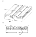
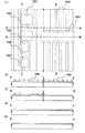
まず、半導体記憶素子の信頼性に関しては、次のような構造上の問題がある。図2に示すのは、絶縁表面を有する基板上に作製された典型的な半導体記憶素子の構造であり、(A)、(B)、(C)はそれぞれ平面図、チャネル長方向断面図、及びチャネル幅方向断面図である。図2において、半導体記憶素子は、絶縁表面を有する基板201上に、半導体活性層202、第1ゲート絶縁膜203、浮遊ゲート電極204、第2ゲート絶縁膜205、制御ゲート電極206が積層された構造となっている。半導体活性層202は、チャネル領域207と、一導電型の不純物が添加された高濃度不純物領域208とからなる。
【0010】
なお、浮遊ゲート電極204は電荷蓄積層の1形態である。また、高濃度不純物領域208の一方は、第1ゲート絶縁膜203を介して浮遊ゲート電極204と一部重なっていてもよい。
【0011】
半導体記憶素子の信頼性に関して問題となるのは、半導体活性層端部209の形状である。図2に示すような半導体活性層形状の場合、制御ゲート電極と活性層間に電位差を与えると、半導体活性層端部の角の部分に電界が集中し、半導体活性層端部209における局所的な電荷注入/放出が起こる。その結果、第1ゲート絶縁膜は、半導体活性層端部209において集中的に劣化してしまい、信頼性が低くなる。
【0012】
電界の集中による局所的な第1ゲート絶縁膜の劣化を防ぐには、半導体活性層端部209のような電界の集中する領域を有さない半導体記憶素子の構造を実現することが効果的である。
【0013】
次に、メモリの動作速度に関しては、絶縁表面を有する基板上に高特性のTFTおよび半導体記憶素子を作製することが重要となる。
【0014】
絶縁表面を有する基板上にTFTを形成する技術は、主に半導体表示装置(代表的には、液晶表示装置、EL表示装置)の研究開発を通して大幅に進歩してきた。例えば、多結晶シリコン膜を用いたTFTは、非晶質シリコン膜を用いたTFTよりも電界効果移動度(モビリティともいう)が高く、従来、基板外の駆動回路で行っていた表示部の制御を、画素と同一の基板上に形成した駆動回路で行うことが可能となった。
【0015】
今後システムオンパネルを視野に入れた場合には、さらなる高速動作を実現する必要があり、より高特性のTFTが要求されている。
【0016】
近年、絶縁表面を有する基板上にTFTを形成する注目される技術の一つに、レーザー光の照射による結晶性半導体膜の作製方法がある。レーザー発振装置としては、通常、エキシマレーザーに代表される気体レーザーや、YAGレーザーに代表される固体レーザーが用いられる。特に、特開2001−144027号公報において、Nd:YVO4レーザーなど固体レーザー発振装置を用いて、その第2高調波であるレーザー光を非晶質半導体膜に照射して、従来に比べ結晶粒径の大きい結晶性半導体膜を形成し、TFTを作製する技術が開示されている。
【0017】
しかしながら、平坦な表面上に形成された非晶質半導体膜にレーザー光を照射して結晶化させると結晶は多結晶となり、結晶欠陥が含まれる結晶粒界の位置を制御することができなかった。また、結晶化に伴って起こる半導体膜の体積収縮や下地との熱応力や格子不整合などによる歪みやクラックが発生するが、この位置を制御することができなかった。
【0018】
その結果、TFTのチャネル領域の結晶性を制御することができず、結局はチャネル領域に含まれる結晶粒界や結晶欠陥によって個々の素子特性がばらつく要因となっていた。
【0019】
つまり、レーザー光の照射によって結晶性半導体膜を作製する場合には、結晶粒界の位置を制御しTFTのチャネル領域の結晶性を制御することが重要な課題となる。
【0020】
また、メモリの高速動作を実現する場合には、TFT特性だけでなく、同時に半導体記憶素子特性を改善することも重要である。つまり、TFT特性の改善により、周辺回路の動作速度が向上し、また、半導体記憶素子特性の改善により半導体記憶素子の駆動能力があがり、読み出し速度が向上する。
【0021】
本発明は上記問題点を鑑みてなされたものであり、チャネル領域において活性層端部での電界集中が起こらない構造の半導体記憶素子を実現し、かつ、結晶粒界や結晶欠陥、クラックの位置を制御することで、チャネル領域には双晶以外の結晶粒界を含まず、電界効果移動度が高く、ばらつきが小さいTFTおよび半導体記憶素子を実現することで、信頼性の高い不揮発性メモリを有する動作の高速な半導体記憶装置を提供することを目的とする。
【0022】
【課題を解決するための手段】
上記問題点を解決するために、本発明の半導体記憶素子は、絶縁表面を有する基板上に直線状凹部が設けられた絶縁膜を形成し、該絶縁膜上に非晶質半導体膜あるいは多結晶半導体膜を形成し、絶縁膜の凹部に半導体膜を溶融して流し込み結晶化させた結晶性半導体膜を形成し、少なくともチャネル領域を形成する部位において結晶性半導体膜の厚みが凹部の深さ以下となるように結晶性半導体膜の表面をエッチング除去し、該結晶性半導体膜の上面部に接する第1ゲート絶縁膜、浮遊ゲート電極、第2ゲート絶縁膜、制御ゲート電極を形成することを特徴とするものである。
【0023】
また、本発明の半導体記憶装置は、半導体記憶素子をマトリクス状に配置してなるメモリセルアレイを有し、該メモリセルアレイは、絶縁表面を有する基板上に複数の直線状凹部をストライプ状に配置したストライプ状凹部が設けられた絶縁膜を形成し、該絶縁膜上に非晶質半導体膜あるいは多結晶半導体膜を形成し、絶縁膜の凹部に半導体膜を溶融して流し込み結晶化させた結晶性半導体膜を形成し、少なくともチャネル領域を形成する部位において結晶性半導体膜の厚みが凹部の深さ以下となるように結晶性半導体膜の表面をエッチング除去し、半導体記憶素子の配置に合わせて結晶性半導体膜の不要な領域をエッチング除去し、該結晶性半導体膜の上面部に接する第1ゲート絶縁膜、浮遊ゲート電極、第2ゲート絶縁膜、制御ゲート電極を形成することを特徴とするものである。
【0024】
また、本発明の他の構成の半導体記憶装置は、半導体記憶素子をマトリクス状に配置してなるメモリセルアレイを有し、該メモリセルアレイは、絶縁表面を有する基板上に複数の直線状凹部をストライプ状に配置したストライプ状凹部と該ストライプ状凹部間を接続するストライプ間凹部とが設けられた絶縁膜を形成し、該絶縁膜上に非晶質半導体膜あるいは多結晶半導体膜を形成し、絶縁膜の凹部に半導体膜を溶融して流し込み結晶化させた結晶性半導体膜を形成し、少なくともチャネル領域を形成する部位において結晶性半導体膜の厚みが凹部の深さ以下となるように結晶性半導体膜の表面をエッチング除去し、半導体記憶素子の配置および半導体記憶素子間の接続に合わせて結晶性半導体膜の不要な領域をエッチング除去し、該結晶性半導体膜の上面部に接する第1ゲート絶縁膜、浮遊ゲート電極、第2ゲート絶縁膜、制御ゲート電極を形成することを特徴とするものである。なお、本構成において、半導体記憶素子を接続する半導体膜配線は、ストライプ間凹部に形成された結晶性半導体膜によって形成される。
【0025】
また、本発明の他の構成の半導体記憶装置は、半導体記憶素子をマトリクス状に配置してなるメモリセルアレイを有し、該メモリセルアレイは、絶縁表面を有する基板上に複数の直線状凹部をストライプ状に配置したストライプ状凹部が設けられた絶縁膜を形成し、該絶縁膜上に非晶質半導体膜あるいは多結晶半導体膜を形成し、絶縁膜の凹部に半導体膜を溶融して流し込み結晶化させた結晶性半導体膜を形成し、半導体記憶素子を接続する半導体膜配線となる領域をフォトレジストでマスクした状態で、少なくともチャネル領域を形成する部位において結晶性半導体膜の厚みが凹部の深さ以下となるように結晶性半導体膜の表面をエッチング除去し、半導体記憶素子の配置および半導体記憶素子を接続する半導体膜配線の配置に合わせて結晶性半導体膜の不要な領域をエッチング除去し、該結晶性半導体膜の上面部に接する第1ゲート絶縁膜、浮遊ゲート電極、第2ゲート絶縁膜、制御ゲート電極を形成することを特徴とするものである。なお、本構成において、半導体記憶素子を接続する半導体膜配線は、結晶性半導体膜の表面をエッチングされず、ストライプ状凹部間を乗り越えて繋がっている結晶性半導体膜によって形成される。
【0026】
なお、半導体記憶装置とは、EEPROM(Electrically Erasable and Programmable Read Only Memory)やフラッシュメモリといった不揮発性メモリ、および、そのような不揮発性メモリを半導体記憶部として有する半導体装置全般を指す。例えば、不揮発性メモリを半導体記憶部として有するマイクロプロセッサ、半導体表示装置(代表的には液晶表示装置およびEL表示装置)、およびこれらを搭載した装置をその範疇に含む。
【0027】
なお、本発明でいう非晶質半導体膜とは、狭義の意味で完全な非晶質構造を有するものだけではなく、微細な結晶粒子が含まれた状態、又はいわゆる微結晶半導体膜、局所的に結晶構造を含む半導体膜を含む。代表的には非晶質シリコン膜が適用され、その他に非晶質シリコンゲルマニウム膜、非晶質シリコンカーバイト膜などを適用することもできる。また、多結晶半導体膜は、これら非晶質半導体膜を公知の方法で結晶化させたものである。
【0028】
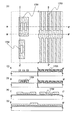
図1に示すのは、上述した本発明の半導体記憶装置を構成する半導体記憶素子の典型的な構造であり、(1)、(2)、(3)はそれぞれ平面図、チャネル長方向断面図、及びチャネル幅方向断面図である。図1において、半導体記憶素子は、絶縁表面を有する基板101上に、絶縁膜109、110によって設けられた直線状凹部に形成された結晶性半導体活性層102、第1ゲート絶縁膜103、浮遊ゲート電極104、第2ゲート絶縁膜105、制御ゲート電極106が積層された構造となっている。結晶性半導体活性層102は、チャネル領域107と、一導電型の不純物が添加された高濃度不純物領域108とからなる。
【0029】
なお、高濃度不純物領域108の一方は、第1ゲート絶縁膜103を介して浮遊ゲート電極104と一部重なっていてもよい。
【0030】
本発明の半導体記憶素子は、少なくともチャネル領域を形成する部位において結晶性半導体膜の厚みが凹部の深さ以下となるように結晶性半導体膜の表面をエッチング除去する工程によって、チャネル領域を形成する結晶性半導体膜の側面が、凹部側壁によって完全に覆われていることを特徴とする。
【0031】
図1に示すように、結晶性半導体活性層の厚さは、絶縁膜109、110の厚さよりも小さくてもよいし、結晶性半導体活性層の厚さは、絶縁膜109、110の厚さと同じであっても良い。
【0032】
上記半導体記憶素子の断面構造は、半導体活性層と第1ゲート絶縁膜との界面に角部はなく平面であるから、半導体活性層端部において電界が集中し、局所的に電荷注入/放出が起こるといったことがなくなる。その結果、第1ゲート絶縁膜の局所的な劣化を防ぐことができ、高い信頼性を実現することが可能となる。
【0033】
なお、上述の半導体記憶装置は、メモリセルを形成する基板上に、メモリセルを選択するデコーダ回路、書き込み・読み出し回路等の周辺回路や、他の半導体集積回路を有していてもよい。その場合、メモリの高速動作を実現するために、周辺回路や他の半導体集積回路を構成するTFTを、上述した方法で形成した結晶性半導体膜を用いて作製することが好ましい。
【0034】
結晶性半導体膜の形成方法についてさらに説明する。
【0035】
上述した直線状凹部あるいはストライプ状凹部はチャネル長方向に延在して設けられている。凹部の幅(チャネル形成領域とする場合におけるチャネル幅)が0.01μm以上2μm以下、好ましくは0.1〜1μmで形成し、その深さは、0.01μm以上3μm以下、好ましくは0.1μm以上2μm以下で形成する。
【0036】
結晶性半導体膜を溶融して結晶化させる手段としては、気体レーザー発振装置、固体レーザー発振装置を光源とするパルス発振又は連続発振レーザー光を適用する。照射するレーザー光は光学系にて線状に集光されたものであり、その強度分布が長手方向において均一な領域を有し、短手方向に分布を持っていても良く、光源として用いるレーザー発振装置は、矩形ビーム固体レーザー発振装置が適用され、特に好ましくは、スラブレーザー発振装置が適用される。
【0037】
線状に集光され長手方向に拡張されたレーザー光又は強光を非晶質半導体膜あるいは多結晶半導体膜に照射し、且つレーザー光の照射位置と半導体膜が形成された基板とを相対的に動かして、レーザー光が一部又は全面を走査することにより半導体膜を溶融させ、その状態を経て結晶化又は再結晶化を行う。レーザー光の走査方向は、絶縁膜に形成された直線状凹部と平行な方向又はトランジスタのチャネル長方向に沿って行う。これによりレーザー光の走査方向に沿って結晶が成長し、結晶粒界がチャネル長方向と交差することを防ぐことができる。
【0038】
凹部の深さを半導体膜の厚さと同程度かそれ以上とすることにより、レーザー光又は強光の照射により溶融した半導体が表面張力により凹部に凝集して固化する。この時、凹部の底端部から結晶成長させることにより、結晶化に伴い発生する歪みは凹部以外の領域に集中する。一方、凹部に充填されるように形成した結晶性半導体膜は歪みから開放することができる。そして、結晶粒界、結晶欠陥を含む凹部周辺に残存する結晶性半導体膜はエッチングにより除去してしまう。
【0039】
上記の如く作製される半導体記憶素子には、絶縁表面上に設けられた直線状凹部において、双晶以外の結晶粒界を含まない結晶性半導体膜が備えられている。
【0040】
上記本発明によって、半導体記憶素子及びTFTにおいて、そのチャネル形成領域の場所を指定して、双晶以外の結晶粒界を含まない結晶性半導体膜を形成することが可能となる。つまり、TFTのチャネル領域の結晶性を制御し、チャネル領域の結晶性を高めることで、電界効果移動度高く、かつ特性ばらつきの小さい半導体記憶素子及びTFTを作製することが可能となる。その結果、TFT特性の改善による周辺回路の高速化と、半導体記憶素子特性の改善による読み出し速度の高速化によって、高速動作を実現した半導体記憶装置を実現することができる。
【0041】
【発明の実施の形態】
(実施形態1)
本発明の半導体記憶装置の実施形態として、不揮発性メモリの回路構成と動作方法について説明する。
【0042】
本発明は、半導体記憶素子の構造や半導体活性層、および周辺回路を構成するTFTの構造や半導体活性層に特徴があり、メモリセルの回路構成や動作方法は公知の技術を用いればよい。本実施の形態では、典型的な不揮発性メモリとして、NOR型フラッシュメモリの回路構成と動作方法について簡単に説明する。
【0043】
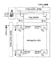
図7に、m×nビットの記憶容量を有するNOR型フラッシュメモリのブロック回路図を示す。図7に示したNOR型フラッシュメモリは、複数のメモリセル(1、1)〜(n、m)が縦m個×横n個のマトリクス状に配置されたメモリセルアレイ701と、Xアドレスデコーダ703、Yアドレスデコーダ702、Yセレクタ704、書き込み・読み出し回路705といった周辺回路によって構成されている。他の周辺回路として、昇圧回路、アドレスバッファ回路等が設けられてもよい。
【0044】
各メモリセル(代表として、メモリセル(i、j)を考える。ここで、iは1以上n以下の整数、jは1以上m以下の整数)は、nチャネル型の半導体記憶素子によって構成される。そして、半導体記憶素子のドレイン電極と制御ゲート電極は、ビット線BL(i)とワード線WL(j)にそれぞれ接続されている。また、ビット線BL(1)〜BL(n)はYアドレスデコーダ702に、ワード線WL(1)〜WL(m)はXアドレスデコーダ703にそれぞれ接続されている。また、全ての半導体記憶素子のソース電極は共通のソース線に接続されており、ソース線電位Vsが与えられている。
【0045】
データの書き込みと読み出しは、Xアドレスデコーダ703およびYアドレスデコーダ702によって選択されたメモリセルにおいて行われる。メモリセル(1、1)を例にとって、ホットエレクトロンによる書き込み動作、読み出し動作ついて説明する。
【0046】
まず、半導体記憶素子にデータを書き込む場合は、ソース線をGNDに落し、ビット線BL(1)およびワード線WL(1)に、それぞれ正の高電圧(例えば16V)を印加する。このような条件下では、半導体記憶素子のドレイン近傍での高電界により、インパクトイオン化が起こる。さらにゲート方向にも高電界が生じるために、発生したホットエレクトロンは浮遊ゲート電極に注入され、書き込みが行われる。半導体記憶素子のしきい値電圧は、浮遊ゲート電極に蓄積された電荷量に応じて変化する。
【0047】
半導体記憶素子に格納されたデータを読み出す場合は、ソース線をGNDに落し、ワード線WL(1)に所定の電圧を印加する。所定の電圧は、半導体記憶素子の浮遊ゲート電極に電荷が蓄積された状態のしきい値電圧と蓄積されない状態のしきい値電圧との間に設定すればよい。その結果、浮遊ゲート電極に電荷が蓄積されている半導体記憶素子がオフ状態に、蓄積されていない半導体記憶素子はオン状態となることを利用して、メモリセル(1、1)に記憶されているデータをビット線BL(1)から読み出す。
【0048】
例えば、半導体記憶素子の2状態のしきい値電圧がそれぞれ2V以下、および4V以上である場合には、所定の電圧として3Vを用いることができる。
【0049】
データの消去は、選択された複数のメモリセルに対して同時に行われる。例えば、第1列目のメモリセル(1,1)〜(m,1)を消去する場合、ソース線およびワード線WL(1)をGNDに落し、ビット線BL(1)に正の高電圧(例えば20V)を印加する。この時、半導体記憶素子のゲート・ドレイン間に高い電位差が生じるため、浮遊ゲート電極に蓄積されている電子がトンネル電流によってドレイン領域へ放出され、消去が行われる。このように、半導体記憶素子のドレイン領域から電荷を引き抜く場合には、ドレイン側の高濃度不純物領域と浮遊ゲート電極とが第1ゲート絶縁膜を介して一部重なっていることが好ましい。
【0050】
なお、書き込み、読み出しおよび消去時において選択されていない信号線BL(2)〜BL(n)、WL(2)〜WL(m)の電位は全て0Vとすればよい。また、上述した動作電圧の値は一例であって、その値に限られるわけではない。
【0051】
なお、本実施形態では、1つの半導体記憶素子に2値(1ビット)の情報を格納する場合を説明したが、1つの半導体記憶素子に3値以上の情報を格納する多値の不揮発性メモリであっても構わない。また、本発明は、NOR型のフラッシュメモリに限られず、NAND型フラッシュメモリやAND型フラッシュメモリについても同様に適用することができる。この他、1つの半導体記憶素子と1つの選択用のTFTでもってメモリセルを構成するタイプの不揮発性メモリであってもよいし、選択用のTFTと半導体記憶素子との役割を合わせ持つスプリットゲート構造の半導体記憶素子でもってメモリセルを構成するタイプの不揮発性メモリであっても構わない。
【0052】
(実施形態2)
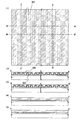
本発明における結晶性半導体膜の形成方法について説明する。説明には、図3〜図6を用いる。図3に示す斜視図には、基板301上に第1絶縁膜302と第2絶縁膜303〜306が形成されており、絶縁膜によってストライプ状凹部が設けられた形態が示されている。なお、図3では直線状凹部が3本示されているが、勿論その数に限定されることはない。
【0053】
基板は市販の無アルカリガラス基板、石英基板、サファイア基板、単結晶又は多結晶半導体基板の表面を絶縁膜で被覆した基板、金属基板の表面を絶縁膜で被覆した基板を適用することができる。
【0054】
なお、サブミクロンのデザインルールでストライプ状凹部を形成するには、基板表面の凹凸、基板のうねり又はねじれを露光装置(特にステッパ)の焦点深度以下にしておく必要があることから、1回の露光領域内における基板表面の凹凸、基板のうねり又はねじれが1μm以下、好ましくは0.5μm以下とすることが望ましい。
【0055】
第2絶縁膜303〜306の幅W2は0.1〜10μm(好ましくは0.5〜1μm)、隣接する第2絶縁膜の間隔W1は0.01〜2μm(好ましくは0.1〜1μm)であり、第2絶縁膜の厚さd1は0.01〜3μm(好ましくは0.1〜2μm)である。また、ストライプパターンは規則的な周期である必要はなく、島状の半導体膜の幅に合わせて所定の間隔で配置させても良い。直線状凹部の長さも限定はなく、例えばTFTのチャネル領域を形成することができる程度の長さがあれば良い。
【0056】
第1絶縁膜は、窒化珪素、窒素含有量が酸素含有量よりも大きな酸窒化珪素、窒化アルミニウム、又は酸窒化アルミニウムから選ばれた材料で、30〜300nmの厚さで形成する。また、所定の形状で凹部が形成された第2絶縁膜は、酸化珪素又は酸窒化珪素で厚さd1が10〜3000nm、好ましくは100〜2000nmとなるように形成する。酸化珪素はオルトケイ酸テトラエチル(Tetraethyl Ortho Silicate:TEOS)とO2とを混合しプラズマCVD(Chemical Vapor Deposition)法で形成することができる。窒酸化珪素膜はSiH4、NH3、N2O又は、SiH4、N2Oを原料として用いプラズマCVD法で形成することができる。
【0057】
図3で示すように、直線状のストライプパターンを二層の絶縁膜で形成する場合には、エッチング加工において第1絶縁膜と第2絶縁膜との間に選択比をもたせる必要がある。実際には、第1絶縁膜よりも第2絶縁膜のエッチング速度が相対的に早くなるように材料及び成膜条件を適宜調整することが望ましい。エッチングの方法としては、緩衝フッ酸を用いたエッチング、又はCHF3を用いたドライエッチングにより行う。このとき、第2絶縁膜で形成される凹部の側面部の角度は5〜120度、好ましくは80〜100度の範囲で適宜設定すれば良い。
【0058】
なお、ここでは結晶性半導体膜を形成する下地の凹凸形状は、第1絶縁膜と第2絶縁膜で形成する一例を示したが、ここで示す形態に限定されず同様な形状を有するものであれば代替することができる。例えば、石英基板の表面をエッチング処理して直接凹部を形成し、凹凸形状を設けても良い。
【0059】
図4で示すように、半導体膜401は珪素、珪素とゲルマニウムの化合物又は合金、珪素と炭素の化合物又は合金を用いて、0.01〜3μm(好ましくは0.1〜1μm)の厚さに形成する。即ち、半導体膜401の厚さd2は第2絶縁膜で形成される凹部の深さと同程度もしくはそれ以上とすることが望ましい。半導体膜401はプラズマCVD法、スパッタリング法、減圧CVD法で形成される非晶質半導体膜又は多結晶半導体膜、或いは、固相成長により形成された多結晶半導体膜などが適用される。半導体膜401は図示するように、下地の第1絶縁膜と第2絶縁膜とで形成される凹凸構造を覆うように形成する。また、第1絶縁膜及び第2絶縁膜の表面に付着した硼素などの化学汚染の影響を排除し、しかもその絶縁表面と非晶質半導体膜が直接に接しないように、非晶質半導体膜の下層側に第3絶縁膜として酸窒化珪素膜を同一の成膜装置内で大気に触れさせることなく連続的に成膜すると良い。
【0060】
そして、この半導体膜401を瞬間的に溶融させ結晶化させる。この結晶化はレーザー光又はランプ光源からの放射光を光学系にて半導体膜が溶融する程度のエネルギー密度に集光して照射する。この工程においては、特に連続発振レーザー発振装置を光源とするレーザー光を適用することが好ましい。適用されるレーザー光は光学系にて線状に集光及び長手方向に拡張されたものであり、その強度分布が長手方向において均一な領域を有し、短手方向に分布を持たせておくことが望ましい。
【0061】
レーザー発振装置は、矩形ビーム固体レーザー発振装置が適用され、特に好ましくは、スラブレーザー発振装置が適用される。スラブ材料としては、Nd:YAG、Nd:GGG(ガドリニウム・ガリウム・ガーネット)、Nd:GsGG(ガドリニウム・スカンジウム・ガリウム・ガーネット)などの結晶が使用される。スラブレーザーでは、この板状のレーザー媒質の中を、全反射を繰り返しながらジグザグ光路で進む。或いは、Nd、Tm、Hoをドープしたロッドを用いた固体レーザー発振装置であり、特にYAG、YVO4、YLF、YAlO3などの結晶にNd、Tm、Hoをドープした結晶を使った固体レーザー発振装置にスラブ構造増幅器を組み合わせたものでも良い。
【0062】
また、連続発振レーザー光の波長は、半導体膜の光吸収係数を考慮して400〜700nmであることが望ましい。このような波長帯の光は、波長変換素子を用いて基本波の第2高調波、第3高調波を取り出すことで得られる。波長変換素子としてはADP(リン酸二水素化アンモニウム)、Ba2NaNb5O15(ニオブ酸バリウムナトリウム)、CdSe(セレンカドミウム)、KDP(リン酸二水素カリウム)、LiNbO3(ニオブ酸リチウム)、Se、Te、LBO、BBO、KB5などが適用される。特にLBOを用いることが望ましい。代表的な一例は、Nd:YVO4レーザー発振装置(基本波1064nm)の第2高調波(532nm)を用いる。また、レーザーの発振モードはTEM00モードであるシングルモードを適用する。
【0063】
また、レーザー光に準ずる強光を照射しても良い。例えば、ハロゲンランプ、キセノンランプ、高圧水銀灯、メタルハライドランプ、エキシマランプから放射される光を反射鏡やレンズなどにより集光したエネルギー密度の高い光であっても良い。
【0064】
最も適した材料として選ばれる珪素の場合、吸収係数が103〜104cm-1である領域はほぼ可視光域にある。ガラスなど可視光透過率の高い基板と、珪素により30〜200nmの厚さをもって形成される非晶質半導体膜を結晶化する場合、波長400〜700nmの可視光域の光を照射することで、当該半導体膜を選択的に加熱して、下地絶縁膜にダメージを与えずに結晶化を行うことができる。具体的には、非晶質珪素膜に対し、波長532nmの光の侵入長は概略100nm〜1000nmであり、膜厚30nm〜200nmで形成される非晶質半導体膜の内部まで十分達することができる。即ち、半導体膜の内側から加熱することが可能であり、レーザー光の照射領域における半導体膜のほぼ全体を均一に加熱することができる。
【0065】
レーザー光は直線状の凹部方向と平行な方向に走査し、溶融した半導体は表面張力が働いて凹部に流れ込み凝固する。凝固した状態では図5で示すように表面がほぼ平坦になる。その結果、凹部上で厚さd3が第2絶縁膜上で厚さd4より大きい結晶性半導体膜501が形成される。こうして形成された結晶性半導体膜501は、結晶の成長端や結晶粒界は第2絶縁膜上に形成され、凹部領域では双晶以外の結晶粒界が含まれないという特徴を有している。
【0066】
その後、好ましくは500〜600℃の加熱処理を行い、結晶性半導体膜に蓄積された歪みを除去すると良い。この歪みは、結晶化によって起こる半導体の体積収縮、下地との熱応力や格子不整合などにより発生するものである。この加熱処理は、通常の熱処理装置を用いて行えば良いが、例えばガス加熱方式の瞬間熱アニール(RTA)法を用いて1〜10分の処理を行えば良い。なお、この工程は本発明において必須な要件ではなく、適宜選択して行えば良いものである。
【0067】
その後図6で示すように、結晶性半導体膜501の表面をエッチングして凹部に埋め込まれている結晶性半導体膜601、602、603を選択的に抽出する。第2絶縁膜上に形成された結晶の成長端や結晶粒界を含む領域をエッチング除去することにより良質な半導体領域のみ残すことができる。またこの時、結晶性半導体膜601、602、603の側面は完全に凹部側壁に覆われるようにする。つまり、結晶性半導体膜601、602、603の厚さd5を第2絶縁膜の厚さd1と同じかそれ以下となるようにする。
【0068】
なお、このような結晶性半導体膜を得るためには、第2絶縁膜の厚さ(凹部の深さ)d1が半導体膜401の厚さd2とほぼ等しいかそれより大きい形態が最も適している。第2絶縁膜の厚さ(凹部の深さ)d1が半導体膜401の厚さd2より小さい場合には、凹部が浅いので結晶性半導体膜501の表面が十分平坦化されることはない。なお、第2絶縁膜の厚さ(凹部の深さ)d1が半導体膜401の厚さd2よりも十分大きい場合には、結晶性半導体膜501が凹部に流れ込み、第2絶縁膜203上には殆ど残存しないようにすることも可能である。また、凹部の幅W2が1μmよりも大きい場合には、第2絶縁膜上に結晶粒界が形成されるだけでなく、凹部の中央付近にも結晶粒界が発生しやすくなる傾向が見られる。これは、間隔が広がることで応力緩和の効果が低減するためであると推定している。
【0069】
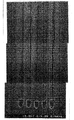
図25で示す走査電子顕微鏡(SEM)写真はその一例を示し、170nmの段差を設け、0.5μmの凹部の幅と間隔を設けた下地絶縁膜上に150nmの非晶質珪素膜を形成して結晶化した結果を示している。結晶性半導体膜の表面は結晶粒界を顕在化させるためにセコ液(HF:H2O=2:1に添加剤としてK2Cr2O7を用いて調合した薬液)でエッチングしてある。
【0070】
図28には、図25で示すSEM写真の見取り図が描かれている。図28において、斜線部2802は、図3に示す第2絶縁膜がある領域であり、斜線部2802に挟まれた領域2803は、凹部領域である。また、太線2801はクラックあるいは結晶粒界を表している。図28および図25から明らかなように、結晶粒界は、第2絶縁膜上に集中しており、凹部領域には顕著な粒界は見られないことが分かる。
【0071】
なお、図28および図25において、レーザ光の走査方向は図面下から上方向である。また、斜線部2802の下側端部では、第2絶縁膜が露出している。これは、レーザ光照射による結晶化工程において、融解した珪素膜がレーザ光の走査方向に移動し固化したためと推測される。
【0072】
図26は凹部に形成される結晶性半導体膜の配向性を反射電子回折パターン(EBSP:Electron Backscatter diffraction Pattern)により求めた結果を示している。EBSPは走査型電子顕微鏡(SEM:Scanning Electron Microscopy)に専用の検出器を設け、電子ビームを結晶面に照射してその菊池線からの結晶方位同定をコンピューターで画像認識させることによって、そのミクロな結晶性を表面配向のみならず、結晶の全方向に関して測定するものである(以下、この手法を便宜上EBSP法と呼ぶ)。
【0073】
図26のデータは、凹部においては線状に集光されたレーザー光の走査方向と平行な方向に結晶が成長していることを示している。成長の面方位は、同一の直線状凹部においてほぼ均一に揃っていることが確認される。
【0074】
また、図27には、170nmの段差を設け、0.5μmの凹部の幅と間隔を設けた下地絶縁膜上に150nmの非晶質珪素膜を形成して結晶化した結果の断面透過電子顕微鏡(Transmission Electron Microscope:TEM)写真を示す。
【0075】
図27に示した写真では、写真中央縦方向にストライプパタンの断面が存在する。ストライプパタンの断面において、暗灰色の領域が第2絶縁膜であり、第2絶縁膜間に形成される凹部と第2絶縁膜上の薄い領域に、結晶性珪素膜が形成されている。第2絶縁膜上の結晶性珪素膜には、黒い領域が見られ、結晶粒界が第2絶縁膜上に集中していることがわかる。凹部に形成された結晶性珪素膜に見られる線状の境界は双晶であり、凹部の結晶性半導体膜には双晶以外の結晶粒界が含まれていないことがわかる。
【0076】
上述した方法により、凹部に双晶以外の結晶粒界を含まない、結晶方位がほぼ均一に揃った結晶性半導体膜を残存させることができる。そして、半導体記憶素子の配置に合わせて、凹部の良質な結晶性半導体膜がチャネル領域となるように活性層を切り出し、第1ゲート絶縁膜及び浮遊ゲート電極を形成する。このような各段階を経て本発明の半導体記憶素子を形成することにより、特性ばらつきが小さく、電流駆動能力の高い半導体記憶素子を実現することが可能となる。
【0077】
同時に、結晶性半導体膜の側面を完全に凹部側壁に覆われるようにすることにより、浮遊ゲート電極への電荷の注入および放出時の活性層端での電界集中のない構造とすることができ、信頼性の高い半導体記憶素子を実現することができる。
【0078】
さらに、上述した方法により、TFTの配置に合わせて、凹部の良質な結晶性半導体膜がチャネル領域となるように活性層を切り出し、ゲート絶縁膜及びゲート電極を形成することで、特性ばらつきが小さく、電流駆動能力の高いTFTを実現することが可能となる。上述した半導体記憶素子およびTFTを用いて、メモリセルおよび周辺回路を同時に形成することにより、信頼性が高く、高速動作可能な半導体記憶装置を実現することができる。
【0079】
(実施形態3)
次に、凹部を有する下地絶縁膜上に結晶性珪素膜を形成し、その凹部に充填された充填領域にチャネル形成領域が配設される半導体記憶素子およびTFTを作製する一形態を図面を用いて説明する。なお、本実施形態の係る各図面において、(1)は上面図、(2)〜(5)はそれに対応する各部位の縦断面図を示す。
【0080】
本実施の形態では、メモリセルアレイと周辺回路とを同時に作製する形態を示し、図面の右側には半導体記憶素子がマトリクス状に配置されたNOR型メモリセルアレイの一部を、左側には、周辺回路を代表して、nチャネル型TFTとpチャネル型TFTにより構成されるインバータを、作製する形態を説明する。
【0081】
図8には、ガラス基板801上に第1絶縁膜802および第2絶縁膜803が形成され、絶縁表面上にストライプ状凹部が形成された形態が示されている。図8に示した形態は、実施形態2において説明した方法によって作製することができる。本実施形態では、第1絶縁膜802を30〜300nmの酸窒化アルミニウムで形成する。第2絶縁膜803はプラズマCVD法でTEOSとO2とを混合し、反応圧力40Pa、基板温度400℃とし、高周波(13.56MHz)電力密度0.6W/cm2で放電させ10〜3000nm、好ましくは100〜2000nmの厚さに酸化珪素膜を堆積し、その後エッチングにより凹部を形成する。凹部の幅は、特にチャネル形成領域が配置される場所において、0.01〜2μm、好ましくは0.1〜1μmで形成する。
【0082】
その後、図9で示すように第1絶縁膜802及び第2絶縁膜803上に酸化膜又は酸窒化珪素膜から成る第3絶縁膜901と非晶質珪素膜を同一のプラズマCVD装置を用い大気に触れさせることなく連続的に成膜する。非晶質珪素膜は珪素を主成分に含む半導体膜で形成し、プラズマCVD法でSiH4を原料気体として用い形成する。非晶質珪素膜は下地の段差形状を反映した平坦でない表面形状が形成される。
【0083】
結晶化は連続発振レーザー光を照射して行う。図9はその結晶化後の状態を示している。結晶化の条件は連続発振モードのYVO4レーザー発振器を用い、その第2高調波(波長532nm)の出力5〜10Wを、光学系にて短手方向に対する長手方向の比が10以上である線状レーザー光に集光し、且つ長手方向に均一なエネルギー密度分布を有するように集光し、10〜200cm/secの速度で走査して結晶化させる。均一なエネルギー密度分布とは、完全に一定であるもの以外を排除することではなく、エネルギー密度分布において許容される範囲は±10%である。
【0084】
線状に集光されたレーザー光の走査方向と凹部の配置との関係は図21に示されている。線状に集光されたレーザー光2160の強度分布はその強度分布が長手方向において均一な領域を有していることが望ましい。これは加熱される半導体の温度が照射領域の温度を一定にすることが目的である。線状に集光されたレーザー光の長手方向(走査方向と交差する方向)に温度分布が生じると、結晶の成長方向をレーザー光の走査方向に限定することができなくなるためである。直線状のストライプパターンは図示のように線状に集光されたレーザー光2160の走査方向と合わせて配列させておくことで、結晶の成長方向と、全てのトランジスタのチャネル長方向とを合わせることができる。これによりトランジスタの素子間の特性ばらつきを小さくすることができる。
【0085】
また、線状に集光されたレーザー光による結晶化は、1回の走査(即ち、一方向)のみで完了させても良いし、より結晶性を高めるためには往復走査しても良い。さらに、レーザー光による結晶化した後、フッ酸などによる酸化物除去、或いは、アンモニア過酸化水素水処理などアルカリ溶液により珪素膜の表面を処理し、エッチング速度の速い品質の悪い部分を選択的に除去して、再度同様の結晶化処理を行っても良い。このようにして、結晶性を高めることができる。
【0086】
この条件でレーザー光を照射することにより、非晶質珪素膜は瞬間的に溶融し結晶化させる。実質的には溶融帯が移動しながら結晶化が進行する。溶融した珪素は表面張力が働いて凹部に凝集し固化する。これにより、図9に示すように凹部を充填する形態で表面が平坦な結晶性珪素膜902が形成される。
【0087】
その後図10に示すように、ソース・ドレイン領域となる領域および結晶性珪素膜を用いた配線となる領域をフォトレジストでマスクした状態で、結晶性珪素膜902の表面をエッチング除去する。この時、フォトレジストでマスクしない領域は、凹部に埋め込まれた結晶性珪素膜のみを残すようにエッチング処理を行う。その結果、少なくともチャネル領域となる部位においては、結晶性珪素膜の側面は完全に凹部を形成する絶縁膜によって覆われる。このエッチング処理により、マスクしない領域は凹部に埋め込まれ、マスクした領域は凹部間が繋がった結晶性珪素膜1001が得られる。結晶性珪素膜はフッ素系のガスと酸素とをエッチングガスとして用いることにより下地の酸化膜と選択性をもってエッチングすることができる。例えば、エッチングガスとして、CF4とO2の混合ガスが適用される。
【0088】
さらに、図10に示す結晶性珪素膜1001から、図11に示す島状の珪素膜1101〜1103を形成する。この島状の珪素膜は、実施形態2で示したように、双晶以外の結晶粒界が含まれないという特徴を有している。なお、図11は、この島状の珪素膜1101〜1103の形状を限定的に示すものではなく、所定のデザインルールに従う範囲内で自由に設計すれば良い。
【0089】
本実施形態では、半導体記憶素子は素子面積を最小にするように一つの直線状凹部に形成される結晶性珪素膜を用いて形成し、また、半導体記憶素子に接続されるソース線を結晶性珪素膜を用いて形成する構成としており、図11に示すような島状の珪素膜1103とした。一方、周辺回路を構成するTFTは、必要な電流駆動能力に応じてチャネル幅を設計する必要があり、複数の直線上凹部に形成される結晶性珪素膜をチャネル領域として用いることで、複数のチャネル領域が並列に配設さたTFT(マルチチャネルTFTと呼ぶ)構成としており、図11に示すような島状の珪素膜1101、1102とした。
【0090】
この後、図12で示すように、島状の珪素膜1101〜1103の上面を覆い、TFTのゲート絶縁膜および半導体記憶素子の第1ゲート絶縁膜として用いる第4絶縁膜1201、TFTのゲート電極および半導体記憶素子の浮遊ゲート電極として用いる導電膜1202、1203、半導体記憶素子の第2ゲート絶縁膜として用いる第5絶縁膜1204、および半導体記憶素子の制御ゲート電極として用いる導電膜1205、を順に形成する。第4絶縁膜1201および第5絶縁膜1204は、公知の気相法(プラズマCVD法、スパッタ法等)を用いて、30〜200nmの酸化珪素膜又は酸窒化珪素膜を形成する。第5絶縁膜1204としてSiO2/SiN/SiO2による積層膜(ONO膜と呼ばれる)を形成してもよい。また、導電膜1202、1203、1205はタングステン又はタングステンを含有する合金、アルミニウム又はアルミニウム合金、多結晶シリコンなどで形成する。
【0091】
なお、絶縁表面を有する基板として石英基板を用いる場合には、半導体記憶素子の第1ゲート絶縁膜として用いる第4絶縁膜1201を、熱酸化工程により形成してもよい。例えば、酸化雰囲気中で950℃の加熱処理を加え、10〜200nmの熱酸化膜を形成する。これにより、良質な酸化膜と界面準位の少ない半導体/絶縁膜界面が得られ、第1ゲート絶縁膜の高い信頼性が得られる。また、第1ゲート絶縁膜は、酸化珪素膜又は酸窒化珪素膜を形成した後、熱酸化工程を行い、堆積膜と熱酸化膜の積層構造としてもよい。この場合も、界面準位の少ない半導体/絶縁膜界面が得られ、高い信頼性が得られる。
【0092】
なお、従来構造の半導体記憶素子において、第1ゲート絶縁膜形成時に熱酸化を行うと、活性層端付近では、活性層底面でも熱酸化が進行し、活性層短部の形状が歪み、その結果、電界の集中による信頼性低下の問題があった。本発明の半導体記憶素子は、半導体活性層の側面が凹部の側壁によって覆われているため、活性層端付近においても活性層上面部で熱酸化が進行するだけであり、従来の活性層底面での熱酸化といった問題は生じない。
【0093】
図13では、島状の半導体膜1101〜1103に一導電型の不純物領域1301〜1303を形成する段階を示している。ここでは、n型不純物領域1302、1303、p型不純物領域1301を設けるものとする。これらの不純物領域はTFTのゲート電極として用いる導電膜1202および半導体記憶素子の制御ゲート電極として用いる導電膜1205をマスクとして自己整合的に形成しても良いし、フォトレジストをマスクとして形成しても良い。不純物領域1301〜1303はソース・ドレイン領域を形成し、必要に応じて低濃度ドレイン領域を適宜設けることもできる。
【0094】
この不純物領域1301〜1303は不純物イオンを電界で加速して、半導体膜に注入するイオン注入法又はイオンドーピング法などが適用される。
【0095】
そして、図14に示すように窒化珪素膜又は酸窒化珪素膜による第6絶縁膜1401を形成し、ソース・ドレイン領域を形成する不純物領域と接触する配線1402を形成する。その後、400〜450℃に熱処理をすることにより窒化珪素膜又は酸窒化珪素膜が含有する水素が放出され島状の半導体膜に対する水素化を行うことができる。
【0096】
こうして、図14に示すように、半導体記憶素子1405からなるNOR型メモリセルアレイと、周辺回路を代表して、nチャネル型マルチチャネルTFT1403、及びpチャネル型マルチチャネルTFT1404からなるインバータ回路と、を形成することができる。もちろん、この構成に限られるわけではなく、公知の他のメモリセルアレイや他のCMOS回路あるいは単極性TFTからなる回路であっても、本実施形態と同様にして作製することができる。また、並列に配設するチャネル形成領域の数に限定はなく、必要に応じて任意個数配設すれば良い。
【0097】
このように、半導体記憶素子およびTFTの配置に合わせて、少なくとも半導体記憶素子のチャネル領域においては結晶性半導体膜の側面が凹部の側壁によって覆われた、双晶以外の結晶粒界を含まない良質な結晶性半導体膜がチャネル領域となるように活性層を切り出し、半導体記憶素子においては、第1ゲート絶縁膜、浮遊ゲート電極、第2ゲート絶縁膜、制御ゲート電極を、TFTにおいては、ゲート絶縁膜およびゲート電極を、それぞれ形成することによって、信頼性が高く、特性ばらつきが小さく、電流駆動能力の高い半導体記憶素子、および特性ばらつきが小さく、電流駆動能力の高いTFTを同時に作製することが可能となる。
【0098】
その結果、半導体記憶素子がマトリクス状に配置されたメモリセルアレイ、およびTFTによって構成される周辺回路が同一基板上に形成された、信頼性が高く、高速動作可能な半導体記憶装置を実現することが可能となる。
【0099】
【実施例】
(実施例1)
本発明は、半導体活性層と制御ゲート電極の間に電荷蓄積層を有する様々な半導体記憶素子に適用することが可能である。特に、電化蓄積層として半導体クラスタ層、金属クラスタ層、あるいは窒化膜を設けた半導体記憶素子に対しても適用することができる。これらの半導体記憶素子は、電荷を蓄積する領域が空間的に離散的に設けられていることを特徴とする。
【0100】
電荷を蓄積する領域として半導体または金属のクラスタ層を用いる半導体記憶素子のチャネル長方向断面図の一例を図19(a)に示す。図19(a)に示した半導体記憶素子は、基板1900上に、チャネル領域1901と一導電型の不純物が添加された不純物領域1902、1903とからなる半導体活性層、第1ゲート絶縁膜1904、クラスタ層1906、第2ゲート絶縁膜1907、および制御ゲート電極1908が順に積層されてなる。クラスタ層1906は、離散的な塊状の半導体または金属(クラスタと呼ぶ)によって構成される層であり、この離散的なクラスタ1905が電荷の捕獲中心としての役割を果たす。
【0101】
電荷を蓄積する領域として窒化膜等を用いる半導体記憶素子としては、MNOS(Metal Nitride Oxide Semiconductor)、MONOS(Metal Oxide Nitride Oxide Semiconductor)等が知られている。MNOS及びMONOS型の半導体記憶素子のチャネル長方向断面図の一例を図19(b)及び(c)にそれぞれ示す。図19(b)示した半導体記憶素子は、基板1910上に、チャネル領域1911と一導電型の不純物が添加された不純物領域1912、1913とからなる半導体活性層、第1ゲート絶縁膜1914、窒化膜1915、および制御ゲート電極1916が順に積層されてなる。また、図19(c)示した半導体記憶素子は、基板1920上に、チャネル領域1921と一導電型の不純物が添加された不純物領域1922、1923とからなる半導体活性層、第1ゲート絶縁膜1924、窒化膜1925、第2ゲート絶縁膜1926、および制御ゲート電極1927が順に積層されてなる。いずれにおいても、窒化膜中の空間的に離散的な不純物準位が電荷の捕獲中心としての役割を果たす。
【0102】
なお、本発明を上述した半導体記憶素子に適用する場合には、チャネル領域として絶縁表面を有する直線状凹部に形成され、側面が完全に凹部側壁に覆われ、双晶以外の結晶粒界を含まない、結晶方位がほぼ均一に揃った結晶性半導体膜を用いれば良い。
【0103】
半導体記憶素子として、電荷を蓄積する領域が離散的に設けられている電荷蓄積層を用いた場合、電荷保持特性が第1ゲート絶縁膜の欠陥やピンホールの影響を受けにくいという効果がある。浮遊ゲート電極を有する半導体記憶素子のように、電荷を蓄積する領域が連続的に設けられている場合には、第1ゲート絶縁膜に一箇所でもピンホールがあると、浮遊ゲート電極に蓄積された電荷は全てそのピンホールからリークしてしまうため、半導体記憶素子の電荷保持特性に大きく影響する。しかし、電荷を蓄積する領域が離散的に設けられている半導体記憶素子を用いた場合には、ピンホールの影響を受ける領域は限定され、多くの電荷蓄積領域はそのピンホールの影響を受けないため、半導体記憶素子の電荷保持特性への影響は少ない。
【0104】
(実施例2)
本発明における結晶性半導体膜の形成において、実施形態2で示すように非晶質半導体膜にレーザー光を照射して結晶化させる方法の他に、固相成長により結晶化した後さらにレーザー光を照射して溶融再結晶化しても良い。
【0105】
例えば、図4において非晶質半導体膜401を形成した後、該非晶質半導体膜(例えば非晶質珪素膜)の結晶化温度を低温化させ配向性を向上させるなど、結晶化を促進する触媒作用のある金属元素としてNiを添加する。Niの添加法に限定はなく、スピン塗布法、蒸着法、スパッタ法などを適用するこができる。スピン塗布法による場合には酢酸ニッケル塩が5ppmの水溶液を塗布して金属元素含有層を形成する。勿論、触媒元素はNiに限定されるものではなく、他の公知の材料を用いても良い。
【0106】
その後、580℃にて4時間の加熱処理により非晶質半導体膜401を結晶化させる。この結晶化した半導体膜に対し、レーザー光又はそれと同等な強光を照射して溶融させ再結晶化する。こうして、図5と同様に表面がほぼ平坦化された結晶性半導体膜501を得ることができる。この結晶性半導体膜501も同様に成長端や結晶粒界が第2絶縁膜304上に形成される。
【0107】
レーザー光の被照射体として結晶化した半導体膜を用いる利点は半導体膜の光吸収係数の変動率にあり、結晶化した半導体膜にレーザー光を照射して溶融させたとしても光吸収係数は殆ど変動しない。よって、レーザー照射条件のマージンを広くとることができる。
【0108】
こうして形成された結晶性半導体膜には金属元素が残存するが、ゲッタリング処理により取り除くことができる。この技術の詳細については、特願2001−019367号出願(又は特願2002−020801号出願)を参照されたい。また、このゲッタリング処理に伴う加熱処理は、結晶性半導体膜の歪みを緩和するという効果も合わせ持っている。
【0109】
その後、実施形態2と同様に凹部の結晶性半導体膜を抽出する。抽出された結晶性半導体膜は、双晶以外の結晶粒界を含まず、結晶方位がほぼ均一に揃っているという特徴を有し、かつ、少なくとも半導体記憶素子のチャネル領域となる部位において側面が凹部の側壁によって覆われている。そして、この結晶性半導体を使って半導体記憶素子およびTFTを作製することができる。
【0110】
なお、本実施例は、実施例1で説明した半導体記憶素子に適用することもできる。
【0111】
(実施例3)
本実施例では、結晶化に際し適用することのできるレーザー処理装置の構成の一例を示す。
【0112】
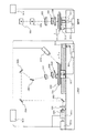
図20はレーザー発振装置2001a、2001b、シャッター2002、高変換ミラー2003〜2006、シリンドリカルレンズ2008、2009、スリット2007、載置台2011、載置台2011をX方向及びY方向に変位させる駆動手段2012、2013、当該駆動手段をコントロールする制御手段2014、予め記憶されたプログラムに基づいてレーザー発振装置2001や制御手段2014に信号を送る情報処理手段2015などから成っているレーザー処理装置の構成を正面図と側面図により示すものである。
【0113】
レーザー発振装置は矩形ビーム固体レーザー発振装置が適用され、特に好ましくは、スラブレーザー発振装置が適用される。或いは、YAG、YVO4、YLF、YAlO3などの結晶にNd、Tm、Hoをドープした結晶を使った固体レーザー発振装置にスラブ構造増幅器を組み合わせたものでも良い。スラブ材料としては、Nd:YAG、Nd:GGG(ガドリニウム・ガリウム・ガーネット)、Nd:GsGG(ガドリニウム・スカンジウム・ガリウム・ガーネット)などの結晶が使用される。その他にも、連続発振可能な気体レーザー発振装置、固体レーザー発振装置を適用することもできる。連続発振固体レーザー発振装置としてはYAG、YVO4、YLF、YAlO3などの結晶にCr、Nd、Er、Ho、Ce、Co、Ti又はTmをドープした結晶を使ったレーザー発振装置を適用する。発振波長の基本波はドープする材料によっても異なるが、1μmから2μmの波長で発振する。5W以上のより高い出力を得る為には、ダイオード励起の固体レーザー発振装置をカスケード接続しても良い。
【0114】
このようなレーザー発振装置から出力される円形状又は矩形状のレーザー光は、シリンドリカルレンズ2008、2009により照射面の断面形状において線状に集光される。また、照射面での干渉を防ぐため、高変換ミラーを適宜調節して10〜80度の角度を持って斜め方向から入射する構成となっている。シリンドリカルレンズ2008、2009は合成石英製とすれば高い透過率が得られ、レンズの表面に施されるコーティングは、レーザー光の波長に対する透過率が99%以上を実現するために適用される。勿論、照射面の断面形状は線状に限定されず、矩形状、楕円形又は長円形など任意な形状としても構わない。いずれにしても短軸と長軸の比が、1対10〜1対100の範囲に含まれるものを指している。また、波長変換素子2010は基本波に対する高調波を得るために備えられている。
【0115】
また、載置台2011を駆動手段2012、2013により二軸方向に動かすことにより基板2020のレーザー処理を可能としている。一方の方向への移動は基板2020の一辺の長さよりも長い距離を1〜200cm/sec、好ましくは5〜50cm/secの等速度で連続的に移動させることが可能であり、他方へは線状ビームの長手方向と同程度の距離を不連続にステップ移動させることが可能となっている。レーザー発振装置2001a、2001bの発振と、載置台2011は、マイクロプロセッサを搭載した情報処理手段2015により同期して作動するようになっている。
【0116】
載置台2011は図中で示すX方向に直線運動をすることにより、固定された光学系から照射されるレーザー光で基板全面の処理を可能としている。位置検出手段2016は基板2020がレーザー光の照射位置にあることを検出して、その信号を情報処理手段2015に伝送し、情報処理手段2015によりレーザー発振装置2001a、2001bの発振動作とのタイミングを同期させている。つまり、基板2020がレーザー光の照射位置にない時は、レーザーの発振を止めその寿命を延長させている。
【0117】
このような構成のレーザー照射装置により基板2020に照射されるレーザー光は、図中に示すX方向又はY方向に相対移動させることにより半導体膜の所望の領域または全面を処理することができる。
【0118】
なお、本実施例は、実施例1、2のいずれの構成とも自由に組み合わせることが可能である。
【0119】
(実施例4)
実施形態2乃至3では、ストライプ状凹部を有する下地絶縁膜上に結晶性半導体膜を形成する場合を説明した。本発明は完全なストライプパタンである必要はなく、少なくとも半導体記憶素子およびTFTのチャネル領域を構成する結晶性半導体膜を直線状凹部にて形成することを特徴としている。例えば、ソース・ドレイン領域や半導体膜を用いた配線領域は、直線状凹部間を接続するストライプ間凹部にて形成された結晶性半導体膜を用いても構わない。このような結晶性半導体膜中には結晶粒界や結晶欠陥が含まれ得るが、ソース・ドレイン領域や半導体膜配線として用いる場合には特に問題とならない。
【0120】
本実施例では、ソース・ドレイン領域や半導体膜を用いた配線領域に合わせて、ストライプ状凹部間を接続するストライプ間凹部を設けた下地絶縁膜を用いて半導体記憶素子およびTFTを作製する工程について説明する。工程の詳細は実施形態3からの差異のみを、図15、図16を用いて説明する。
【0121】
図15は第1絶縁膜1501とストライプ状凹部およびストライプ間凹部を形成する第2絶縁膜1502を形成した状態を示している。図中点線で囲む領域1503は、メモリセルアレイにおけるソース配線となる部位であり、ソース配線となる領域に合わせて凹部が設けられている。また、図中点線で囲む領域1504〜1507は、TFTのソース・ドレイン領域となる部位である。
【0122】
次いで、この上に非晶質半導体膜を堆積し、それに線状に集光されたレーザー光を照射して結晶性半導体膜を形成した後、第2絶縁膜1502上にある結晶性半導体膜をエッチングにより除去し、凹部を充填する形で結晶性半導体膜を抽出する。図16は、さらに、半導体記憶素子およびTFTを構成する半導体膜の配置と半導体膜配線の配置に合わせて、この結晶性半導体膜をエッチングして、島状の半導体膜1601、1602、1603を形成した状態を示している。
【0123】
そして、半導体記憶素子の配置に合わせて第1ゲート絶縁膜、浮遊ゲート電極、第2ゲート絶縁膜、及び制御ゲート電極を、TFTの配置に合わせてゲート絶縁膜及びゲート電極を、それぞれ形成する。その後、n型又はp型の不純物領域を形成し、層間絶縁膜を介して各種配線を形成することにより、実施形態3と同様、メモリセルアレイと周辺回路とを同時に作製することができる。
【0124】
このように、下地絶縁膜にソース・ドレイン領域や半導体膜を用いた配線領域に合わせた凹部を予め設けることによって、実施形態3で説明した、ソース・ドレイン領域や半導体膜を用いた配線領域をカバーするマスクは不要となり、半導体記憶装置の作製に必要なマスク枚数を1枚削減することが可能となる。
【0125】
なお、本実施例は、実施例1〜3のいずれの構成とも自由に組み合わせることが可能である。
【0126】
(実施例5)
本実施例では、メモリセルアレイと周辺回路とを同時に作製する別の方法を説明する。本発明の半導体記憶素子は、チャネル領域を構成する結晶性半導体膜の側面が凹部側壁によって覆われていることを特徴とするが、メモリセルを選択するデコーダ回路、書き込み・読み出し回路等の周辺回路や他の半導体集積回路を構成する同一基板上のTFTはそのような構造である必要はない。
【0127】
特に、周辺回路や他の半導体集積回路を構成するTFTのチャネル領域を構成する結晶性半導体膜の側面を覆う凹部側壁を除去することによって、結晶性半導体膜の上面だけでなく、側面部もチャネル領域とする構造とし、電流駆動能力の高いTFTを実現することができる。
【0128】
工程の詳細は実施形態3からの差異のみを図17、図18を用いて説明する。
【0129】
図17は、実施形態3に従って図11まで作製した後、半導体記憶素子が配置される領域(図中、右半分)をフォトレジストでマスクした状態で、第2絶縁膜をエッチング処理により除去した状態を示している。このエッチング処理は緩衝フッ酸のよる薬液処理、又はCHF3を用いたドライエッチングなどで行うことができる。
【0130】
この工程により、図17に示すように、TFTのチャネル領域となる島状の半導体膜1701、1702の側面部及び上面部が露出した状態となる。この部分にゲートを形成することによって、島状の半導体膜1701、1702の側面部及び上面部をチャネル形成領域とすることができる。
【0131】
なお、本実施例では、第1絶縁膜までエッチングを行ったが、第2絶縁膜の途中でエッチングを止めても良い。エッチングの深さを調節することにより島状の半導体膜1701、1702のチャネル形成領域の深さを調節することができる。即ち、結晶化領域を選択することができる。
【0132】
そして、図18に示すように、半導体記憶素子の配置に合わせて、結晶性半導体膜の上面部に重畳して第1ゲート絶縁膜、浮遊ゲート電極、第2ゲート絶縁膜、及び制御ゲート電極を、TFTの配置に合わせて結晶性半導体膜の側面部と上面部に重畳してゲート絶縁膜及びゲート電極を、それぞれ形成する。
【0133】
その後、n型又はp型の不純物領域を形成し、層間絶縁膜を介して各種配線を形成することにより、実施形態3と同様、メモリセルアレイと周辺回路とを同時に作製することができる。
【0134】
このような構成とすることによって、半導体記憶素子においては、チャネル領域を構成する結晶性半導体膜の側面が凹部側壁に覆われ、浮遊ゲート電極への電荷の注入および放出時に活性層端部での電界集中のない構造とするにより、高い信頼性を実現することができ、周辺回路を構成するTFTにおいては、結晶性半導体膜の側面部と上面部においてチャネルが形成され実効的にチャネル幅が増加することにより、電流駆動能力を向上させることができる。
【0135】
なお、本実施例は、実施例1〜4のいずれの構成とも自由に組み合わせることが可能である。
【0136】
(実施例6)
本発明の半導体記憶装置の例として、不揮発性メモリをワンチップ上に集積化されたRISCプロセッサ、ASICプロセッサ等のマイクロプロセッサに適用した場合について説明する。
【0137】
図22に示すのは、マイクロプロセッサの一例である。マイクロプロセッサは典型的にはCPUコア2201、フラッシュメモリ2204、クロックコントローラ2203、キャッシュメモリ2202、キャッシュコントローラ2205、割り込みコントローラ2206、I/Oポート2207等から構成される。もちろん、図22に示すマイクロプロセッサは簡略化した一例であり、実際のマイクロプロセッサはその用途によって多種多様な回路設計が行われる。
【0138】
図22に示すマイクロプロセッサは、実施形態あるいは実施例に示した作製方法によって作製され、凹部を有する下地絶縁膜上に結晶性珪素膜を形成し、その凹部に充填された充填領域にチャネル形成領域が配設される半導体記憶素子およびTFTによって構成されている。フラッシュメモリ2204には本発明の半導体記憶素子が用いられている。キャッシュメモリとしては、例えばSRAMが用いられている。
【0139】
このように本発明をマイクロプロセッサに応用することにより、信頼性の高い不揮発性メモリを有し、高速動作可能な半導体記憶装置を実現することができる。動作速度として、デザインルール等にも依存するが、フラッシュメモリの読み出しサイクルとして500nsec以下、CPUの動作周波数として5MHz以上が実現される。
【0140】
なお、本実施例は、実施の形態及び実施例1〜5のいずれの構成とも組み合わせることが可能である。
【0141】
(実施例7)
本実施例では、絶縁表面を有する基板上に画像表示部(代表的には、液晶表示部あるいはEL表示部)、不揮発性メモリ、および他の半導体集積回路とを一体形成したシステムオンパネルの形態をとる半導体記憶装置の一例を、図23を用いて説明する。
【0142】
図23において、半導体記憶装置は、画素領域2300、走査線駆動回路2301、信号線駆動回路2302、VRAM2303、フラッシュメモリ2304、CPU2305、画像処理回路2306、ワークメモリ2307及びインターフェース回路2308が、絶縁表面を有する基板2310上に一体形成されてなる。
【0143】
図23に示した半導体記憶装置は、画像データを取り込み、または作製して、画像データの加工とフォーマット変換を行い、画像を表示する装置である。半導体記憶装置としては、例えば、ビデオカメラ、カーナビゲーション、パーソナルコンピュータ、ゲーム機等を考えることができる。
【0144】
半導体記憶装置は、それぞれの形態に応じて、入力端子から画像データの基となるデータを受信する。例えば、放送受信機ではアンテナからの入力データであり、ビデオカメラではCCDからの入力データである。DVテープやメモリーカードからの入力データであってもよい。入力端子からは、この他、キーボードからの入力信号や他の制御信号を入力してもよい。入力された画像の基となるデータは、インターフェース回路2308およびシステムバスを介して、フラッシュメモリ2304格納にされたり、ワークメモリ2307に一時的に格納されたり、あるいは、画像処理回路2306によって画像信号に変換され、VRAMに格納される。画像処理回路2306では、MPEG規格やテープフォーマット等に従って圧縮符号化された画像データの復号処理、画像の補間やリサイズといった画像信号処理が行われる。また、入力された制御信号は、CPUや画像処理回路との通信に用いられるほか、信号線駆動回路や走差線駆動回路に入力される。
【0145】
CPU2305は、フラッシュメモリ2304、ワークメモリ2307、インターフェース回路2308、および他の回路を制御する。また、画像データの基となるデータを作成したり、加工したりする。フラッシュメモリ2304は画像データを作成または加工する場合に必要となる色データや文字データを格納するメモリ領域、あるいはプログラムデータが格納されるメモリ領域として用いらる。ワークメモリ2307は画像データやその基となるデータを格納するメモリ領域、CPUによる制御を行う際のワークメモリ領域等として用いられ、DRAMやSRAMが用いられる。
【0146】
信号線駆動回路2302、走査線駆動回路2301、画素領域2300によって構成される画像表示部は、画像を表示する領域である。信号線駆動回路2302および走査線駆動回路2301には、外部からインターフェース回路を介して制御信号が入力され、信号線駆動回路2302は制御信号に従って、画像処理回路2306から出力されVRAMに格納された画像データを取り込み、画素領域にて画像を表示する。
【0147】
以上のようにして、画像データを取り込みまたは作製して画像を表示する、不揮発性メモリを有する半導体記憶装置が構成される。図23に示す半導体記憶装置は、実施形態あるいは実施例に示した作製方法によって作製され、凹部を有する下地絶縁膜上に結晶性珪素膜を形成し、その凹部に充填された充填領域にチャネル形成領域が配設される半導体記憶素子およびTFTによって構成されている。フラッシュメモリ2304には本発明の半導体記憶素子が用いられている。
【0148】
このように本発明を半導体記憶装置に応用することにより、信頼性の高い不揮発性メモリを有し、高速動作可能な半導体記憶装置を実現することができる。なお、一体形成することで、小型化、消費電力の低減といった効果がある。
【0149】
なお、信号線駆動回路2302、走査線駆動回路2301、画素領域2300によって構成される画像表示部と、他の回路によって構成される画像処理部とは、異なる基板上に作製されてもよい。半導体記憶装置としては、画像処理部を構成する基板でもって、放送受信機や表示部を持たないゲーム機といった形態を構成することができる。もちろん、複数の基板を実装することで上述した半導体記憶装置を実現してもよい。
【0150】
本実施例は、実施例1〜5と組み合わせて用いることが可能である。
【0151】
(実施例8)
本発明を用いて様々な装置を完成させることができる。その一例は、携帯情報端末(電子手帳、モバイルコンピュータ、携帯電話など)、ビデオカメラ、デジタルカメラ、パーソナルコンピュータ、テレビ受像器、投影型表示装置などが挙げられる。それらの一例を図24に示す。
【0152】
図24(A)は本発明を適用してテレビ受像器を完成させる一例であり、筐体2401、支持台2402、表示部2403などにより構成されている。本発明によりガラス基板上に作製される半導体記憶素子を用いることで、信頼性の高い不揮発性メモリを有し、かつ、動作速度の速いテレビ受像器を完成させることができる。
【0153】
図24(B)は本発明を適用してビデオカメラを完成させた一例であり、本体2411、表示部2412、音声入力部2413、操作スイッチ2414、バッテリー2415、受像部2416などにより構成されている。本発明によりガラス基板上に作製される半導体記憶素子を用いることで、信頼性の高い不揮発性メモリを有し、かつ、動作速度の速いビデオカメラを完成させることができる。
【0154】
図24(C)は本発明を適用してノート型のパーソナルコンピュータを完成させた一例であり、本体2421、筐体2422、表示部2423、キーボード2424などにより構成されている。本発明によりガラス基板上に作製される半導体記憶素子を用いることで、信頼性の高い不揮発性メモリを有し、かつ、動作速度の速いパーソナルコンピュータを完成させることができる。
【0155】
図24(D)は本発明を適用してPDA(Personal Digital Assistant)を完成させた一例であり、本体2431、スタイラス2432、表示部2433、操作ボタン2434、外部インターフェース2435などにより構成されている。本発明によりガラス基板上に作製される半導体記憶素子を用いることで、信頼性の高い不揮発性メモリを有し、かつ、動作速度の速いPDAを完成させることができる。
【0156】
図24(E)は本発明を適用して音響再生装置を完成させた一例であり、具体的には車載用のオーディオ装置であり、本体2441、表示部2442、操作スイッチ2443、2444などにより構成されている。本発明によりガラス基板上に作製される半導体記憶素子を用いることで、信頼性の高い不揮発性メモリを有し、かつ、動作速度の速いオーディオ装置を完成させることができる。
【0157】
図24(F)は本発明を適用してデジタルカメラを完成させた一例であり、本体2451、表示部(A)2452、接眼部2453、操作スイッチ2454、表示部(B)2455、バッテリー2456などにより構成されている。本発明によりガラス基板上に作製される半導体記憶素子を用いることで、信頼性の高い不揮発性メモリを有し、かつ、動作速度の速いデジタルカメラを完成させることができる。
【0158】
図24(G)は本発明を適用して携帯電話を完成させた一例であり、本体2461、音声出力部2462、音声入力部2463、表示部2464、操作スイッチ2465、アンテナ2466などにより構成されている。本発明によりガラス基板上に作製される半導体記憶素子を用いることで、信頼性の高い不揮発性メモリを有し、かつ、動作速度の速い携帯電話を完成させることができる。
【0159】
なお、ここで示す装置はごく一例であり、これらの用途に限定するものではない。
【0160】
本実施例は、実施例1〜5と組み合わせて用いることが可能である。
【0161】
【発明の効果】
本発明によって、半導体記憶素子のチャネル領域を形成する部位において、側面が凹部側壁によって覆われた結晶性半導体膜を作製することが可能となる。
【0162】
その結果、半導体活性層端部の電界集中に伴う、第1ゲート絶縁膜の局所的な劣化を抑えることができ、信頼性の高い半導体記憶素子を実現することが可能となる。
【0163】
本発明によって、同時に、結晶化に伴う歪み又は応力を凹部以外の領域に集中させることができ、凹部において双晶以外の結晶粒界を含まない良質な結晶性半導体膜を作製することが可能となる。
【0164】
このようにして、チャネル領域の結晶性を制御し、チャネル領域の結晶性を高めることで、電界効果移動度高く、かつ特性ばらつきの小さい半導体記憶素子及びTFTを作製することが可能となる。
【0165】
上述した半導体記憶素子およびTFTを用いて、メモリセルおよび周辺回路を同時に形成することにより、信頼性が高く、高速動作可能な半導体記憶装置を実現することができる。
【図面の簡単な説明】
【図1】 本発明の半導体記憶素子の上面図及び断面図。
【図2】 従来の半導体記憶素子の上面図及び断面図。
【図3】 本発明の結晶化方法を説明する斜視図。
【図4】 本発明の結晶化方法を説明する斜視図。
【図5】 本発明で結晶化方法を説明する斜視図。
【図6】 本発明の結晶化方法を説明する斜視図。
【図7】 NOR型の不揮発性メモリのブロック回路図。
【図8】 本発明の半導体記憶装置の作製工程を説明する上面図及び断面図。
【図9】 本発明の半導体記憶装置の作製工程を説明する上面図及び断面図。
【図10】 本発明の半導体記憶装置の作製工程を説明する上面図及び断面図。
【図11】 本発明の半導体記憶装置の作製工程を説明する上面図及び断面図。
【図12】 本発明の半導体記憶装置の作製工程を説明する上面図及び断面図。
【図13】 本発明の半導体記憶装置の作製工程を説明する上面図及び断面図。
【図14】 本発明の半導体記憶装置の作製工程を説明する上面図及び断面図。
【図15】 本発明の半導体記憶装置の作製工程を説明する上面図及び断面図。
【図16】 本発明の半導体記憶装置の作製工程を説明する上面図及び断面図。
【図17】 本発明の半導体記憶装置の作製工程を説明する上面図及び断面図。
【図18】 本発明の半導体記憶装置の作製工程を説明する上面図及び断面図。
【図19】 本発明が適用される半導体記憶素子の断面図。
【図20】 本発明に適用するレーザー照射装置の一態様を示す配置図。
【図21】 本発明における線状に集光されたレーザー光とその走査方向を説明する図。
【図22】 マイクロプロセッサの一例を示す図。
【図23】 半導体記憶装置の一例を示す図。
【図24】 半導体記憶装置の一例を示す図。
【図25】 ストライプ状凹部を設けた下地絶縁膜上に150nmの非晶質珪素膜を形成して結晶化したときの表面状態を表す走査電子顕微鏡(SEM)写真(セコエッチ後)。
【図26】 凹部に形成された結晶の配向を示すEBSPマッピングデータ。
【図27】 凹部に形成された結晶の断面透過電子顕微鏡(TEM)写真。
【図28】 図25に示した走査電子顕微鏡(SEM)写真の見取り図。[0001]
[Technical field to which the invention belongs]
The present invention relates to a semiconductor memory element, and more particularly to a thin film transistor having a charge storage layer. The present invention also relates to a thin film transistor having a charge storage layer and a semiconductor memory device in which the thin film transistor is formed over a substrate having an insulating surface.
[0002]
[Prior art]
EEPROM (Electrically Erasable and Programmable Read Only Memory) and flash memory are known as representative memories of semiconductor nonvolatile memory. Since these are non-volatile, unlike DRAM (Dynamic Random Access Memory) and SRAM (Static RAM), which represent semiconductor memories, data is not lost even when the power is turned off. Further, when compared with a magnetic disk representing another nonvolatile memory, it has excellent characteristics in terms of integration density, impact resistance, power consumption, writing / reading speed, and the like.
[0003]
As described above, the semiconductor non-volatile memory has characteristics suitable for portable devices, and application development to portable devices is being promoted. In particular, flash memories with high integration density have been widely applied, and in recent years, multi-value memories that further improve the integration degree have been commercialized. Of course, these are nonvolatile memories on a single crystal silicon substrate (see, for example, Non-Patent Document 1).
[0004]
[Non-Patent Document 1]
Fujio Takaoka, 7 others, "Flash Memory Technology Forum 2000", Science Forum, Inc., July 18, 2000
[0005]
On the other hand, with the spread of portable devices having a display unit such as a mobile phone, there is an increasing demand for a system-on-panel in which a display unit and a logic circuit unit are integrally formed on a substrate having an insulating surface. Along with this, a technique for manufacturing a nonvolatile memory on a substrate having an insulating surface has been required.
[0006]
[Problems to be solved by the invention]
When a nonvolatile memory is manufactured on a substrate having an insulating surface, a memory cell array is formed of semiconductor memory elements, and peripheral circuits such as a decoder circuit for selecting a memory cell and a write / read circuit are thin film transistors (hereinafter referred to as TFTs). The form which comprises is considered.
[0007]
In the present invention, a semiconductor memory element refers to a thin film transistor having a charge storage layer surrounded by an insulating film between a semiconductor active layer and a gate electrode. For example, a structure having a floating gate electrode, an MNOS structure, or a MONOS A thin film transistor having a structure is included in its category.
[0008]
When considering such a nonvolatile memory, improvement of the reliability of the semiconductor memory element accompanied by charge injection and charge discharge into the charge storage layer and improvement of the operation speed of the peripheral circuits are important issues.
[0009]
First, regarding the reliability of the semiconductor memory element, there are the following structural problems. FIG. 2 shows a structure of a typical semiconductor memory element manufactured over a substrate having an insulating surface. (A), (B), and (C) are a plan view, a channel length direction cross-sectional view, And a channel width direction sectional view. In FIG. 2, in the semiconductor memory element, a semiconductor
[0010]
Note that the
[0011]
A problem regarding the reliability of the semiconductor memory element is the shape of the semiconductor
[0012]
In order to prevent local degradation of the first gate insulating film due to electric field concentration, it is effective to realize a structure of a semiconductor memory element that does not have an electric field concentration region such as the semiconductor
[0013]
Next, with respect to the operation speed of the memory, it is important to manufacture high-performance TFTs and semiconductor memory elements on a substrate having an insulating surface.
[0014]
The technology for forming TFTs on a substrate having an insulating surface has greatly advanced mainly through research and development of semiconductor display devices (typically, liquid crystal display devices and EL display devices). For example, a TFT using a polycrystalline silicon film has higher field effect mobility (also referred to as mobility) than a TFT using an amorphous silicon film, and control of a display portion that has been conventionally performed by a driver circuit outside the substrate. Can be performed by a driving circuit formed on the same substrate as the pixel.
[0015]
In the future, when a system-on-panel is taken into consideration, it is necessary to realize higher-speed operation, and TFTs with higher characteristics are required.
[0016]
In recent years, one of the technologies that attract attention that forms TFTs on a substrate having an insulating surface is a method for manufacturing a crystalline semiconductor film by laser light irradiation. As the laser oscillation device, a gas laser represented by an excimer laser or a solid laser represented by a YAG laser is usually used. In particular, in Japanese Patent Application Laid-Open No. 2001-144027, Nd: YVO Four Using a solid-state laser oscillation device such as a laser, the amorphous semiconductor film is irradiated with laser light, which is the second harmonic, to form a crystalline semiconductor film having a larger crystal grain size than before, and a TFT is manufactured. Technology is disclosed.
[0017]
However, when an amorphous semiconductor film formed on a flat surface is crystallized by irradiating laser light, the crystal becomes polycrystalline, and the position of the crystal grain boundary including crystal defects cannot be controlled. . In addition, the semiconductor film volume shrinkage caused by crystallization, distortion or cracks due to thermal stress or lattice mismatch with the substrate, etc. occur, but this position could not be controlled.
[0018]
As a result, the crystallinity of the channel region of the TFT cannot be controlled, and eventually the individual device characteristics vary due to crystal grain boundaries and crystal defects included in the channel region.
[0019]
In other words, when a crystalline semiconductor film is formed by laser light irradiation, it is an important issue to control the crystallinity of the TFT channel region by controlling the position of the crystal grain boundary.
[0020]
Further, when realizing high-speed memory operation, it is important to improve not only the TFT characteristics but also the semiconductor memory element characteristics at the same time. That is, the improvement of the TFT characteristics increases the operation speed of the peripheral circuit, and the improvement of the characteristics of the semiconductor memory element increases the driving capability of the semiconductor memory element, thereby improving the reading speed.
[0021]
The present invention has been made in view of the above problems, and realizes a semiconductor memory element having a structure in which electric field concentration does not occur at the end of the active layer in the channel region, and the position of crystal grain boundaries, crystal defects, and cracks. By controlling the above, the channel region does not include crystal grain boundaries other than twins, and the field effect mobility is high and the variation is small. An object of the present invention is to provide a high-speed semiconductor memory device.
[0022]
[Means for Solving the Problems]
In order to solve the above problems, in a semiconductor memory element of the present invention, an insulating film provided with a linear recess is formed on a substrate having an insulating surface, and an amorphous semiconductor film or a polycrystalline film is formed on the insulating film. A semiconductor film is formed, and a crystalline semiconductor film is formed by melting and pouring the semiconductor film into a concave portion of the insulating film to crystallize, and the thickness of the crystalline semiconductor film is not more than the depth of the concave portion at least at a site where a channel region is formed. The surface of the crystalline semiconductor film is removed by etching so that the first gate insulating film, the floating gate electrode, the second gate insulating film, and the control gate electrode are in contact with the upper surface portion of the crystalline semiconductor film. It is what.
[0023]
The semiconductor memory device of the present invention has a memory cell array in which semiconductor memory elements are arranged in a matrix, and the memory cell array has a plurality of linear recesses arranged in stripes on a substrate having an insulating surface. Crystallinity formed by forming an insulating film provided with stripe-shaped recesses, forming an amorphous semiconductor film or a polycrystalline semiconductor film on the insulating film, and melting and pouring the semiconductor film into the recesses of the insulating film The surface of the crystalline semiconductor film is removed by etching so that the thickness of the crystalline semiconductor film is equal to or less than the depth of the recess at least in a region where the channel region is formed, and a crystal is formed in accordance with the arrangement of the semiconductor memory element. An unnecessary region of the crystalline semiconductor film is removed by etching, and a first gate insulating film, a floating gate electrode, a second gate insulating film, and a control gate electrode that are in contact with the upper surface portion of the crystalline semiconductor film are removed. It is characterized in that to form the.
[0024]
According to another aspect of the present invention, a semiconductor memory device includes a memory cell array in which semiconductor memory elements are arranged in a matrix, and the memory cell array stripes a plurality of linear recesses on a substrate having an insulating surface. Forming an insulating film provided with stripe-shaped concave portions arranged in a shape and inter-stripe concave portions connecting the stripe-shaped concave portions, and forming an amorphous semiconductor film or a polycrystalline semiconductor film on the insulating film to A crystalline semiconductor film is formed by melting and pouring a semiconductor film into a concave portion of the film and crystallizing the crystalline semiconductor film so that the thickness of the crystalline semiconductor film is equal to or less than the depth of the concave portion at least at a portion where a channel region is formed. The surface of the film is etched away, and unnecessary regions of the crystalline semiconductor film are removed by etching in accordance with the arrangement of the semiconductor memory elements and the connection between the semiconductor memory elements. The first gate insulating film in contact with the upper surface of the conductive film, a floating gate electrode, the second gate insulating film, and is characterized in forming a control gate electrode. In this configuration, the semiconductor film wiring for connecting the semiconductor memory element is formed by a crystalline semiconductor film formed in the recess between stripes.
[0025]
According to another aspect of the present invention, a semiconductor memory device includes a memory cell array in which semiconductor memory elements are arranged in a matrix, and the memory cell array stripes a plurality of linear recesses on a substrate having an insulating surface. An insulating film provided with stripe-shaped recesses arranged in a row, an amorphous semiconductor film or a polycrystalline semiconductor film is formed on the insulating film, and the semiconductor film is melted and poured into the recesses of the insulating film for crystallization In the state in which the crystalline semiconductor film is formed, and the region to be the semiconductor film wiring for connecting the semiconductor memory element is masked with a photoresist, the thickness of the crystalline semiconductor film is at least the depth of the recess in the portion where the channel region is formed. The surface of the crystalline semiconductor film is etched away so that the following is achieved in accordance with the arrangement of the semiconductor memory element and the arrangement of the semiconductor film wiring connecting the semiconductor memory element. An unnecessary region of the crystalline semiconductor film is removed by etching to form a first gate insulating film, a floating gate electrode, a second gate insulating film, and a control gate electrode in contact with the upper surface portion of the crystalline semiconductor film It is. Note that in this configuration, the semiconductor film wiring for connecting the semiconductor memory element is formed of a crystalline semiconductor film that is not etched on the surface of the crystalline semiconductor film but is connected across the stripe-shaped recesses.
[0026]
Note that the semiconductor memory device refers to a nonvolatile memory such as an EEPROM (Electrically Erasable and Programmable Read Only Memory) or a flash memory, and a general semiconductor device having such a nonvolatile memory as a semiconductor memory unit. For example, the category includes a microprocessor having a nonvolatile memory as a semiconductor storage unit, a semiconductor display device (typically, a liquid crystal display device and an EL display device), and a device in which these are mounted.
[0027]
Note that the amorphous semiconductor film referred to in the present invention is not limited to a film having a completely amorphous structure in a narrow sense, but includes a state in which fine crystal particles are included, or a so-called microcrystalline semiconductor film, a local Includes a semiconductor film including a crystal structure. Typically, an amorphous silicon film is applied, and in addition, an amorphous silicon germanium film, an amorphous silicon carbide film, or the like can also be applied. The polycrystalline semiconductor film is obtained by crystallizing these amorphous semiconductor films by a known method.
[0028]
FIG. 1 shows a typical structure of a semiconductor memory element constituting the semiconductor memory device of the present invention described above. (1), (2), and (3) are a plan view and a channel length direction sectional view, respectively. FIG. 5 is a cross-sectional view in the channel width direction. In FIG. 1, a semiconductor memory element includes a crystalline semiconductor
[0029]
Note that one of the high-
[0030]
In the semiconductor memory element of the present invention, the channel region is formed by a step of etching and removing the surface of the crystalline semiconductor film so that the thickness of the crystalline semiconductor film is equal to or less than the depth of the recess at least in a region where the channel region is formed. The side surface of the crystalline semiconductor film is completely covered with the side wall of the recess.
[0031]
As shown in FIG. 1, the thickness of the crystalline semiconductor active layer may be smaller than the thickness of the insulating
[0032]
Since the cross-sectional structure of the semiconductor memory element is a flat surface with no corners at the interface between the semiconductor active layer and the first gate insulating film, the electric field is concentrated at the edge of the semiconductor active layer, and charge injection / discharge is locally performed. Nothing happens. As a result, local degradation of the first gate insulating film can be prevented, and high reliability can be realized.
[0033]
Note that the above-described semiconductor memory device may include a peripheral circuit such as a decoder circuit, a write / read circuit, and other semiconductor integrated circuits on a substrate on which the memory cell is formed, and the like. In that case, in order to realize high-speed operation of the memory, it is preferable to manufacture a TFT constituting a peripheral circuit or another semiconductor integrated circuit using the crystalline semiconductor film formed by the above-described method.
[0034]
A method for forming a crystalline semiconductor film will be further described.
[0035]
The linear recesses or stripe-like recesses described above are provided so as to extend in the channel length direction. The width of the recess (channel width in the case of forming a channel formation region) is 0.01 μm or more and 2 μm or less, preferably 0.1 to 1 μm, and the depth is 0.01 μm or more and 3 μm or less, preferably 0.1 μm. The thickness is 2 μm or less.
[0036]
As a means for melting and crystallizing the crystalline semiconductor film, pulsed oscillation or continuous oscillation laser light using a gas laser oscillation device or a solid laser oscillation device as a light source is applied. The laser light to be irradiated is focused in a linear shape by an optical system, and the intensity distribution may have a uniform region in the longitudinal direction and may be distributed in the lateral direction. As the oscillation device, a rectangular beam solid laser oscillation device is applied, and a slab laser oscillation device is particularly preferably applied.
[0037]
Irradiate an amorphous semiconductor film or a polycrystalline semiconductor film with laser light or strong light condensed in a linear shape and extended in the longitudinal direction, and the irradiation position of the laser light and the substrate on which the semiconductor film is formed are relative to each other. Then, the semiconductor film is melted by scanning a part or the whole surface of the laser beam, and crystallization or recrystallization is performed through this state. The scanning direction of the laser light is performed in a direction parallel to the linear recess formed in the insulating film or in the channel length direction of the transistor. As a result, the crystal grows along the scanning direction of the laser beam, and the crystal grain boundary can be prevented from crossing the channel length direction.
[0038]
By setting the depth of the recesses to be equal to or greater than the thickness of the semiconductor film, the semiconductor melted by the irradiation with laser light or strong light aggregates and solidifies in the recesses due to surface tension. At this time, by causing the crystal to grow from the bottom end portion of the concave portion, the distortion generated along with the crystallization is concentrated in a region other than the concave portion. On the other hand, the crystalline semiconductor film formed so as to fill the recesses can be free from strain. Then, the crystalline semiconductor film remaining around the recess including crystal grain boundaries and crystal defects is removed by etching.
[0039]
The semiconductor memory element manufactured as described above includes a crystalline semiconductor film that does not include a crystal grain boundary other than twins in a linear recess provided on an insulating surface.
[0040]
According to the present invention, in the semiconductor memory element and the TFT, it is possible to designate the location of the channel formation region and form a crystalline semiconductor film that does not include crystal grain boundaries other than twins. That is, by controlling the crystallinity of the channel region of the TFT and increasing the crystallinity of the channel region, it is possible to manufacture a semiconductor memory element and a TFT with high field effect mobility and small characteristic variation. As a result, it is possible to realize a semiconductor memory device that realizes high-speed operation by increasing the peripheral circuit speed by improving the TFT characteristics and increasing the read speed by improving the semiconductor memory element characteristics.
[0041]
DETAILED DESCRIPTION OF THE INVENTION
(Embodiment 1)
As an embodiment of the semiconductor memory device of the present invention, a circuit configuration and an operation method of a nonvolatile memory will be described.
[0042]
The present invention is characterized by the structure of the semiconductor memory element, the semiconductor active layer, and the structure of the TFT constituting the peripheral circuit and the semiconductor active layer, and a known technology may be used for the circuit configuration and operation method of the memory cell. In this embodiment, a circuit configuration and an operation method of a NOR flash memory as a typical nonvolatile memory will be briefly described.
[0043]
FIG. 7 shows a block circuit diagram of a NOR type flash memory having a storage capacity of m × n bits. The NOR flash memory shown in FIG. 7 includes a memory cell array 701 in which a plurality of memory cells (1, 1) to (n, m) are arranged in a matrix of m vertical × n horizontal, and an X address decoder 703. , A Y address decoder 702, a Y selector 704, and a write /
[0044]
Each memory cell (typically, a memory cell (i, j) is considered. Here, i is an integer of 1 to n and j is an integer of 1 to m) is constituted by an n-channel semiconductor memory element. The The drain electrode and the control gate electrode of the semiconductor memory element are connected to the bit line BL (i) and the word line WL (j), respectively. The bit lines BL (1) to BL (n) are connected to the Y address decoder 702, and the word lines WL (1) to WL (m) are connected to the X address decoder 703, respectively. Further, the source electrodes of all the semiconductor memory elements are connected to a common source line, and are supplied with a source line potential Vs.
[0045]
Data writing and reading are performed in the memory cell selected by the X address decoder 703 and the Y address decoder 702. Taking a memory cell (1, 1) as an example, a write operation and a read operation using hot electrons will be described.
[0046]
First, when data is written in the semiconductor memory element, the source line is dropped to GND, and a positive high voltage (for example, 16 V) is applied to the bit line BL (1) and the word line WL (1), respectively. Under such conditions, impact ionization occurs due to a high electric field in the vicinity of the drain of the semiconductor memory element. Further, since a high electric field is generated also in the gate direction, the generated hot electrons are injected into the floating gate electrode and writing is performed. The threshold voltage of the semiconductor memory element changes according to the amount of charge accumulated in the floating gate electrode.
[0047]
When reading data stored in the semiconductor memory element, the source line is dropped to GND and a predetermined voltage is applied to the word line WL (1). The predetermined voltage may be set between a threshold voltage in a state where charges are accumulated in the floating gate electrode of the semiconductor memory element and a threshold voltage in a state where charges are not accumulated. As a result, the semiconductor memory element in which the charge is accumulated in the floating gate electrode is turned off, and the semiconductor memory element that is not accumulated is turned on, so that it is stored in the memory cell (1, 1). Data is read from the bit line BL (1).
[0048]
For example, when the two-state threshold voltages of the semiconductor memory element are 2 V or less and 4 V or more, 3 V can be used as the predetermined voltage.
[0049]
Data is erased simultaneously for a plurality of selected memory cells. For example, when erasing the memory cells (1, 1) to (m, 1) in the first column, the source line and the word line WL (1) are dropped to GND, and a positive high voltage is applied to the bit line BL (1). (For example, 20V) is applied. At this time, since a high potential difference is generated between the gate and the drain of the semiconductor memory element, electrons accumulated in the floating gate electrode are emitted to the drain region by a tunnel current, and erasing is performed. As described above, when the charge is extracted from the drain region of the semiconductor memory element, it is preferable that the high-concentration impurity region on the drain side and the floating gate electrode partially overlap with each other through the first gate insulating film.
[0050]
Note that the potentials of the signal lines BL (2) to BL (n) and WL (2) to WL (m) that are not selected at the time of writing, reading, and erasing may be 0V. Moreover, the value of the operating voltage described above is an example, and the value is not limited to that value.
[0051]
In this embodiment, the case where binary (1 bit) information is stored in one semiconductor memory element has been described. However, a multi-value nonvolatile memory that stores information of three values or more in one semiconductor memory element. It does not matter. Further, the present invention is not limited to the NOR type flash memory, but can be similarly applied to a NAND type flash memory and an AND type flash memory. In addition, it may be a non-volatile memory of a type that constitutes a memory cell with one semiconductor memory element and one selection TFT, or a split gate having the role of the selection TFT and the semiconductor memory element. A non-volatile memory of a type that constitutes a memory cell with a semiconductor memory element having a structure may be used.
[0052]
(Embodiment 2)
A method for forming a crystalline semiconductor film in the present invention will be described. 3 to 6 are used for the description. The perspective view shown in FIG. 3 shows a form in which a first
[0053]
As the substrate, a commercially available non-alkali glass substrate, a quartz substrate, a sapphire substrate, a substrate obtained by coating the surface of a single crystal or polycrystalline semiconductor substrate with an insulating film, or a substrate obtained by coating the surface of a metal substrate with an insulating film can be applied.
[0054]
In order to form a stripe-shaped recess with a sub-micron design rule, it is necessary to keep the unevenness of the substrate surface, the undulation or twist of the substrate below the depth of focus of the exposure apparatus (especially a stepper). It is desirable that the unevenness of the substrate surface in the exposure region, the waviness or twist of the substrate is 1 μm or less, preferably 0.5 μm or less.
[0055]
The width W2 of the second insulating
[0056]
The first insulating film is made of silicon nitride, a material selected from silicon oxynitride, aluminum nitride, or aluminum oxynitride having a nitrogen content larger than the oxygen content, and is formed to a thickness of 30 to 300 nm. Further, the second insulating film in which the concave portion is formed in a predetermined shape is formed of silicon oxide or silicon oxynitride so that the thickness d1 is 10 to 3000 nm, preferably 100 to 2000 nm. Silicon oxide is composed of tetraethyl orthosilicate (TEOS) and O 2 And can be formed by a plasma CVD (Chemical Vapor Deposition) method. Silicon nitride oxide film is SiH Four , NH Three , N 2 O or SiH Four , N 2 It can be formed by plasma CVD using O as a raw material.
[0057]
As shown in FIG. 3, when a linear stripe pattern is formed by two layers of insulating films, it is necessary to provide a selection ratio between the first insulating film and the second insulating film in the etching process. Actually, it is desirable to appropriately adjust the material and the film forming conditions so that the etching rate of the second insulating film is relatively faster than that of the first insulating film. Etching using buffered hydrofluoric acid or CHF Three Performed by dry etching using At this time, the angle of the side surface portion of the recess formed by the second insulating film may be appropriately set in the range of 5 to 120 degrees, preferably 80 to 100 degrees.
[0058]
Note that, here, an example in which the uneven shape of the base on which the crystalline semiconductor film is formed is formed using the first insulating film and the second insulating film, but is not limited to the form shown here and has a similar shape. It can be replaced if there is one. For example, the concave surface may be formed directly by etching the surface of the quartz substrate to provide an uneven shape.
[0059]
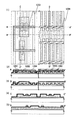
As shown in FIG. 4, the
[0060]
Then, the
[0061]
As the laser oscillation device, a rectangular beam solid-state laser oscillation device is applied, and a slab laser oscillation device is particularly preferably applied. Crystals such as Nd: YAG, Nd: GGG (gadolinium / gallium / garnet), Nd: GsGG (gadolinium / scandium / gallium / garnet) are used as the slab material. A slab laser travels in a zigzag optical path through this plate-like laser medium while repeating total reflection. Alternatively, it is a solid state laser oscillation device using a rod doped with Nd, Tm, and Ho, especially YAG, YVO. Four , YLF, YAlO Three A slab structure amplifier may be combined with a solid-state laser oscillation device using a crystal doped with Nd, Tm, or Ho.
[0062]
The wavelength of the continuous wave laser beam is preferably 400 to 700 nm in consideration of the light absorption coefficient of the semiconductor film. Light in such a wavelength band is obtained by taking out the second harmonic and the third harmonic of the fundamental wave using a wavelength conversion element. As wavelength conversion element, ADP (ammonium dihydrogen phosphate), Ba 2 NaNb Five O 15 (Sodium barium niobate), CdSe (selenium cadmium), KDP (potassium dihydrogen phosphate), LiNbO Three (Lithium niobate), Se, Te, LBO, BBO, KB Five Etc. apply. It is particularly desirable to use LBO. A typical example is Nd: YVO Four The second harmonic (532 nm) of the laser oscillation device (fundamental wave 1064 nm) is used. Further, a single mode which is a TEM00 mode is applied as the laser oscillation mode.
[0063]
Moreover, you may irradiate the strong light according to a laser beam. For example, light having a high energy density obtained by condensing light emitted from a halogen lamp, xenon lamp, high-pressure mercury lamp, metal halide lamp, or excimer lamp by a reflecting mirror or a lens may be used.
[0064]
In the case of silicon selected as the most suitable material, the absorption coefficient is 10 Three -10 Four cm -1 The region which is is almost in the visible light region. When crystallizing a substrate having a high visible light transmittance such as glass and an amorphous semiconductor film formed with a thickness of 30 to 200 nm using silicon, by irradiating light in the visible light region with a wavelength of 400 to 700 nm, Crystallization can be performed without selectively damaging the base insulating film by selectively heating the semiconductor film. Specifically, the penetration depth of light with a wavelength of 532 nm is approximately 100 nm to 1000 nm with respect to the amorphous silicon film, and can sufficiently reach the inside of the amorphous semiconductor film formed with a film thickness of 30 nm to 200 nm. . That is, it is possible to heat from the inside of the semiconductor film, and almost the entire semiconductor film in the laser light irradiation region can be heated uniformly.
[0065]
The laser beam scans in a direction parallel to the linear recess direction, and the molten semiconductor flows into the recess due to surface tension and solidifies. In the solidified state, the surface becomes almost flat as shown in FIG. As a result, a
[0066]
After that, heat treatment is preferably performed at 500 to 600 ° C. to remove distortion accumulated in the crystalline semiconductor film. This distortion occurs due to semiconductor volume shrinkage caused by crystallization, thermal stress with the base, or lattice mismatch. This heat treatment may be performed using a normal heat treatment apparatus. For example, a gas heating rapid thermal annealing (RTA) method may be used for 1 to 10 minutes. Note that this step is not an essential requirement in the present invention, and may be selected as appropriate.
[0067]
Thereafter, as shown in FIG. 6, the surface of the
[0068]
In order to obtain such a crystalline semiconductor film, a configuration in which the thickness (recess depth) d1 of the second insulating film is approximately equal to or larger than the thickness d2 of the
[0069]
The scanning electron microscope (SEM) photograph shown in FIG. 25 shows an example. A 150 nm amorphous silicon film is formed on a base insulating film provided with a step of 170 nm and a width and interval of a recess of 0.5 μm. The results of crystallization are shown. The surface of the crystalline semiconductor film is a seco liquid (HF: H) in order to reveal the grain boundary. 2 O = 2: 1 K as additive 2 Cr 2 O 7 Etched with a chemical solution prepared using
[0070]
FIG. 28 shows a sketch of the SEM photograph shown in FIG. 28, a hatched
[0071]
In FIGS. 28 and 25, the scanning direction of the laser light is from the bottom to the top. Further, the second insulating film is exposed at the lower end of the hatched
[0072]
FIG. 26 shows the result of obtaining the orientation of the crystalline semiconductor film formed in the concave portion by a reflected electron diffraction pattern (EBSP). EBSP provides a scanning electron microscope (SEM) with a dedicated detector, which irradiates the crystal plane with an electron beam and causes the computer to recognize the crystal orientation from the Kikuchi line. The crystallinity is measured not only on the surface orientation but also in all directions of the crystal (hereinafter, this method is referred to as EBSP method for convenience).
[0073]
The data in FIG. 26 indicates that the crystal grows in the direction parallel to the scanning direction of the laser beam condensed linearly in the concave portion. It is confirmed that the growth plane orientation is almost uniform in the same linear recess.
[0074]
Further, FIG. 27 shows a cross-sectional transmission electron microscope as a result of crystallization by forming a 150 nm amorphous silicon film on a base insulating film having a step of 170 nm and a width and interval of a recess of 0.5 μm. (Transmission Electron Microscope: TEM) A photograph is shown.
[0075]
In the photograph shown in FIG. 27, a stripe pattern cross section exists in the longitudinal direction of the photograph center. In the cross section of the stripe pattern, the dark gray region is the second insulating film, and the crystalline silicon film is formed in the recess formed between the second insulating films and the thin region on the second insulating film. It can be seen that a black region is seen in the crystalline silicon film on the second insulating film, and crystal grain boundaries are concentrated on the second insulating film. It can be seen that the linear boundaries seen in the crystalline silicon film formed in the recess are twins, and the crystal semiconductor film in the recess does not contain crystal grain boundaries other than twins.
[0076]
According to the above-described method, a crystalline semiconductor film having substantially uniform crystal orientations that does not include crystal grain boundaries other than twins in the recesses can be left. Then, in accordance with the arrangement of the semiconductor memory element, the active layer is cut out so that the high-quality crystalline semiconductor film in the recess becomes the channel region, and the first gate insulating film and the floating gate electrode are formed. By forming the semiconductor memory element of the present invention through each of these steps, it is possible to realize a semiconductor memory element with small characteristic variation and high current driving capability.
[0077]
At the same time, by completely covering the side surfaces of the crystalline semiconductor film with the sidewalls of the recesses, it is possible to obtain a structure without electric field concentration at the active layer edge during charge injection and emission to the floating gate electrode, A highly reliable semiconductor memory element can be realized.
[0078]
Further, by the above-described method, the active layer is cut out so that the high-quality crystalline semiconductor film of the recess becomes a channel region in accordance with the arrangement of the TFT, and the gate insulating film and the gate electrode are formed. Thus, it is possible to realize a TFT having a high current driving capability. By forming the memory cell and the peripheral circuit at the same time using the semiconductor memory element and the TFT described above, a semiconductor memory device with high reliability and capable of operating at high speed can be realized.
[0079]
(Embodiment 3)
Next, a semiconductor memory element and a TFT in which a crystalline silicon film is formed over a base insulating film having a recess and a channel formation region is provided in the filling region filled in the recess are used with reference to the drawings. I will explain. In each drawing according to the present embodiment, (1) is a top view, and (2) to (5) are longitudinal sectional views of corresponding parts.
[0080]
In this embodiment mode, a memory cell array and a peripheral circuit are manufactured at the same time. A part of a NOR type memory cell array in which semiconductor memory elements are arranged in a matrix is shown on the right side of the drawing, and a peripheral circuit is shown on the left side. As an example, a mode of manufacturing an inverter including an n-channel TFT and a p-channel TFT will be described.
[0081]
FIG. 8 shows a form in which a first
[0082]
After that, as shown in FIG. 9, a third
[0083]
Crystallization is performed by irradiating a continuous wave laser beam. FIG. 9 shows the state after the crystallization. The crystallization conditions are YVO in continuous oscillation mode. Four Using a laser oscillator, the output of 5 to 10 W of the second harmonic (wavelength 532 nm) is condensed into linear laser light having a ratio of the longitudinal direction to the transverse direction of 10 or more in the optical system, and the longitudinal direction. Are condensed so as to have a uniform energy density distribution, and are crystallized by scanning at a speed of 10 to 200 cm / sec. A uniform energy density distribution does not exclude anything that is completely constant, but the allowable range in the energy density distribution is ± 10%.
[0084]
The relationship between the scanning direction of the laser beam condensed linearly and the arrangement of the recesses is shown in FIG. It is desirable that the intensity distribution of the
[0085]
Further, the crystallization by the laser beam condensed linearly may be completed by only one scan (that is, one direction), or may be reciprocated to improve the crystallinity. Furthermore, after crystallizing with laser light, the surface of the silicon film is treated with an alkali solution such as oxide removal with hydrofluoric acid or ammonia hydrogen peroxide solution treatment, and the poor quality part with high etching rate is selectively used. It may be removed and the same crystallization treatment may be performed again. In this way, crystallinity can be increased.
[0086]
By irradiating laser light under these conditions, the amorphous silicon film is instantaneously melted and crystallized. In practice, crystallization proceeds while the melting zone moves. The molten silicon is agglomerated and solidified in the recesses due to surface tension. As a result, as shown in FIG. 9, a
[0087]
Thereafter, as shown in FIG. 10, the surface of the
[0088]
Further, island-shaped
[0089]
In this embodiment, the semiconductor memory element is formed using a crystalline silicon film formed in one linear recess so as to minimize the element area, and the source line connected to the semiconductor memory element is crystalline. An island-shaped
[0090]
Thereafter, as shown in FIG. 12, the upper surface of the island-
[0091]
Note that in the case where a quartz substrate is used as the substrate having an insulating surface, the fourth insulating
[0092]
In the conventional semiconductor memory element, if thermal oxidation is performed at the time of forming the first gate insulating film, thermal oxidation proceeds on the bottom of the active layer near the edge of the active layer, and the shape of the short portion of the active layer is distorted. There was a problem of lowering reliability due to concentration of electric field. In the semiconductor memory element of the present invention, since the side surface of the semiconductor active layer is covered with the side wall of the recess, thermal oxidation proceeds only on the upper surface of the active layer even near the edge of the active layer. There is no problem of thermal oxidation.
[0093]
FIG. 13 shows a step of forming one conductivity
[0094]
For the
[0095]
Then, as shown in FIG. 14, a sixth
[0096]
Thus, as shown in FIG. 14, a NOR type memory cell array composed of
[0097]
As described above, in accordance with the arrangement of the semiconductor memory element and the TFT, at least in the channel region of the semiconductor memory element, the side surface of the crystalline semiconductor film is covered by the side wall of the recess and does not include a crystal grain boundary other than twins. An active layer is cut out so that a crystalline semiconductor film becomes a channel region. In a semiconductor memory element, a first gate insulating film, a floating gate electrode, a second gate insulating film, and a control gate electrode are formed. By forming the film and the gate electrode respectively, it is possible to simultaneously manufacture a semiconductor memory element with high reliability, small characteristic variation, and high current drive capability, and a TFT with low characteristic variation and high current drive capability. It becomes.
[0098]
As a result, it is possible to realize a highly reliable and high-speed semiconductor memory device in which a memory cell array in which semiconductor memory elements are arranged in a matrix and a peripheral circuit including TFTs are formed on the same substrate. It becomes possible.
[0099]
【Example】
Example 1
The present invention can be applied to various semiconductor memory elements having a charge storage layer between a semiconductor active layer and a control gate electrode. In particular, the present invention can also be applied to a semiconductor memory element provided with a semiconductor cluster layer, a metal cluster layer, or a nitride film as a charge storage layer. These semiconductor memory elements are characterized in that charge accumulation regions are spatially discretely provided.
[0100]
FIG. 19A shows an example of a cross-sectional view in the channel length direction of a semiconductor memory element using a semiconductor or metal cluster layer as a region for accumulating charges. 19A includes a semiconductor active layer including a
[0101]
Known semiconductor memory elements using a nitride film or the like as a region for accumulating charges include MNOS (Metal Nitride Oxide Semiconductor), MONOS (Metal Oxide Nitride Oxide Semiconductor), and the like. Examples of cross-sectional views in the channel length direction of MNOS and MONOS type semiconductor memory elements are shown in FIGS. 19B and 19C, respectively. In the semiconductor memory element shown in FIG. 19B, a semiconductor active layer including a
[0102]
When the present invention is applied to the semiconductor memory element described above, it is formed as a linear recess having an insulating surface as a channel region, the side surface is completely covered by the recess side wall, and includes crystal grain boundaries other than twins. A crystalline semiconductor film having a substantially uniform crystal orientation may be used.
[0103]
When a charge storage layer in which charge storage regions are discretely provided is used as a semiconductor memory element, there is an effect that the charge retention characteristics are not easily affected by defects in the first gate insulating film or pinholes. In the case where a region for accumulating charges is continuously provided as in a semiconductor memory element having a floating gate electrode, if there is even a pinhole in the first gate insulating film, it is accumulated in the floating gate electrode. All the charges leaked from the pinholes greatly affect the charge retention characteristics of the semiconductor memory element. However, when a semiconductor memory element in which charge accumulation regions are provided discretely is used, the region affected by the pinhole is limited, and many charge accumulation regions are not affected by the pinhole. Therefore, the influence on the charge retention characteristics of the semiconductor memory element is small.
[0104]
(Example 2)
In the formation of the crystalline semiconductor film in the present invention, in addition to the method of crystallizing an amorphous semiconductor film by irradiating the amorphous semiconductor film with laser as shown in
[0105]
For example, after forming the
[0106]
Thereafter, the
[0107]
The advantage of using a crystallized semiconductor film as an object to be irradiated with laser light is the variation rate of the light absorption coefficient of the semiconductor film. Even if the crystallized semiconductor film is irradiated with laser light and melted, the light absorption coefficient is almost Does not fluctuate. Therefore, a wide margin of laser irradiation conditions can be taken.
[0108]
A metal element remains in the crystalline semiconductor film thus formed, but can be removed by gettering treatment. For details of this technique, refer to Japanese Patent Application No. 2001-019367 (or Japanese Patent Application No. 2002-020801). Further, the heat treatment accompanying the gettering treatment has an effect of alleviating distortion of the crystalline semiconductor film.
[0109]
Thereafter, the recessed crystalline semiconductor film is extracted as in the second embodiment. The extracted crystalline semiconductor film has the characteristics that it does not include crystal grain boundaries other than twins and the crystal orientation is almost uniform, and the side surface is at least a portion that becomes a channel region of a semiconductor memory element. It is covered by the side wall of the recess. Then, a semiconductor memory element and a TFT can be manufactured using this crystalline semiconductor.
[0110]
Note that this embodiment can also be applied to the semiconductor memory element described in
[0111]
(Example 3)
In this embodiment, an example of a configuration of a laser processing apparatus that can be applied in crystallization is shown.
[0112]
FIG. 20 shows
[0113]
As the laser oscillation device, a rectangular beam solid-state laser oscillation device is applied, and a slab laser oscillation device is particularly preferably applied. Or YAG, YVO Four , YLF, YAlO Three A slab structure amplifier may be combined with a solid-state laser oscillation device using a crystal doped with Nd, Tm, or Ho. Crystals such as Nd: YAG, Nd: GGG (gadolinium / gallium / garnet), Nd: GsGG (gadolinium / scandium / gallium / garnet) are used as the slab material. In addition, a gas laser oscillation device and a solid laser oscillation device capable of continuous oscillation can also be applied. As continuous wave solid state laser oscillators, YAG, YVO Four , YLF, YAlO Three A laser oscillation device using a crystal doped with Cr, Nd, Er, Ho, Ce, Co, Ti, or Tm is applied. The fundamental wave of the oscillation wavelength varies depending on the material to be doped, but oscillates at a wavelength of 1 μm to 2 μm. In order to obtain a higher output of 5 W or more, diode-pumped solid state laser oscillation devices may be cascaded.
[0114]
Circular or rectangular laser light output from such a laser oscillation device is condensed linearly in the cross-sectional shape of the irradiated surface by the
[0115]
In addition, the
[0116]
The mounting table 2011 linearly moves in the X direction shown in the drawing, so that the entire surface of the substrate can be processed with laser light emitted from a fixed optical system. The
[0117]
The laser light irradiated to the
[0118]
This embodiment can be freely combined with any of the configurations of the first and second embodiments.
[0119]
Example 4
In
[0120]
In this embodiment, a process for manufacturing a semiconductor memory element and a TFT using a base insulating film provided with an inter-stripe recess that connects between stripe-shaped recesses in accordance with a source / drain region or a wiring region using a semiconductor film. explain. Only the differences from the third embodiment will be described in detail with reference to FIGS. 15 and 16.
[0121]
FIG. 15 shows a state in which the first insulating
[0122]
Next, an amorphous semiconductor film is deposited thereon, and a crystalline semiconductor film is formed by irradiating it with a linearly focused laser beam, and then the crystalline semiconductor film over the second
[0123]
Then, a first gate insulating film, a floating gate electrode, a second gate insulating film, and a control gate electrode are formed in accordance with the arrangement of the semiconductor memory elements, and a gate insulating film and a gate electrode are formed in accordance with the arrangement of the TFTs. Thereafter, an n-type or p-type impurity region is formed, and various wirings are formed through an interlayer insulating film, whereby a memory cell array and a peripheral circuit can be manufactured simultaneously as in the third embodiment.
[0124]
As described above, by providing the base insulating film with recesses corresponding to the wiring regions using the source / drain regions and the semiconductor film, the wiring regions using the source / drain regions and the semiconductor film described in the third embodiment are formed. A mask to be covered becomes unnecessary, and the number of masks necessary for manufacturing a semiconductor memory device can be reduced by one.
[0125]
In addition, a present Example can be freely combined with any structure of Examples 1-3.
[0126]
(Example 5)
In this embodiment, another method for simultaneously manufacturing a memory cell array and a peripheral circuit will be described. The semiconductor memory element of the present invention is characterized in that the side surface of the crystalline semiconductor film constituting the channel region is covered with the side wall of the recess, but the peripheral circuit such as a decoder circuit or a write / read circuit for selecting a memory cell The TFTs on the same substrate constituting other semiconductor integrated circuits do not have to have such a structure.
[0127]
In particular, not only the top surface of the crystalline semiconductor film but also the side surface portion is channeled by removing the recess side walls covering the side surfaces of the crystalline semiconductor film constituting the channel region of the TFT constituting the peripheral circuit and other semiconductor integrated circuits. A structure having a region and a TFT with high current driving capability can be realized.
[0128]
Only the differences from the third embodiment will be described in detail with reference to FIGS. 17 and 18.
[0129]
FIG. 17 shows a state in which the second insulating film is removed by an etching process in a state where the region where the semiconductor memory element is arranged (right half in the drawing) is masked with a photoresist after being manufactured up to FIG. 11 according to the third embodiment. Is shown. This etching process is a chemical process using buffered hydrofluoric acid, or CHF. Three It can be performed by dry etching using
[0130]
By this step, as shown in FIG. 17, the side surface portions and the upper surface portions of the island-shaped
[0131]
In this embodiment, the etching is performed up to the first insulating film, but the etching may be stopped in the middle of the second insulating film. By adjusting the etching depth, the depth of the channel formation region of the island-shaped
[0132]
Then, as shown in FIG. 18, the first gate insulating film, the floating gate electrode, the second gate insulating film, and the control gate electrode are superimposed on the upper surface portion of the crystalline semiconductor film in accordance with the arrangement of the semiconductor memory elements. A gate insulating film and a gate electrode are formed so as to overlap with the side surface portion and the upper surface portion of the crystalline semiconductor film in accordance with the arrangement of the TFT.
[0133]
Thereafter, an n-type or p-type impurity region is formed, and various wirings are formed through an interlayer insulating film, whereby a memory cell array and a peripheral circuit can be manufactured simultaneously as in the third embodiment.
[0134]
With such a configuration, in the semiconductor memory element, the side surface of the crystalline semiconductor film constituting the channel region is covered with the side wall of the recess, and the charge is injected into and released from the floating gate electrode at the end of the active layer. High reliability can be realized by adopting a structure that does not concentrate the electric field. In the TFT constituting the peripheral circuit, a channel is formed on the side surface and the top surface of the crystalline semiconductor film, effectively increasing the channel width. By doing so, the current drive capability can be improved.
[0135]
In addition, a present Example can be freely combined with any structure of Examples 1-4.
[0136]
(Example 6)
As an example of the semiconductor memory device of the present invention, a case where a nonvolatile memory is applied to a microprocessor such as a RISC processor or an ASIC processor integrated on one chip will be described.
[0137]
FIG. 22 shows an example of a microprocessor. The microprocessor typically includes a
[0138]
The microprocessor illustrated in FIG. 22 is manufactured by the manufacturing method described in the embodiment or the example, and a crystalline silicon film is formed over a base insulating film having a recess, and a channel formation region is formed in the filling region filled in the recess. The semiconductor memory element and the TFT are provided. The
[0139]
Thus, by applying the present invention to a microprocessor, a semiconductor memory device having a highly reliable nonvolatile memory and capable of operating at high speed can be realized. Although the operation speed depends on the design rule and the like, a read cycle of the flash memory of 500 nsec or less and a CPU operation frequency of 5 MHz or more are realized.
[0140]
Note that this example can be combined with any of the configurations of the embodiment and Examples 1 to 5.
[0141]
(Example 7)
In this embodiment, an image display unit (typically a liquid crystal display unit or an EL display unit), a nonvolatile memory, and another semiconductor integrated circuit are integrally formed on a substrate having an insulating surface. An example of a semiconductor memory device taking the above will be described with reference to FIG.
[0142]
23, the semiconductor memory device includes a pixel region 2300, a scanning line driver circuit 2301, a signal line driver circuit 2302, a VRAM 2303, a flash memory 2304, a
[0143]
The semiconductor memory device shown in FIG. 23 is a device that captures or creates image data, processes the image data, converts the format, and displays an image. As the semiconductor memory device, for example, a video camera, a car navigation system, a personal computer, a game machine, etc. can be considered.
[0144]
The semiconductor memory device receives data serving as a basis of image data from an input terminal in accordance with each form. For example, it is input data from an antenna in a broadcast receiver, and input data from a CCD in a video camera. It may be input data from a DV tape or a memory card. In addition to this, an input signal from the keyboard or another control signal may be input from the input terminal. The data that is the basis of the input image is stored in the flash memory 2304, temporarily stored in the work memory 2307 via the interface circuit 2308 and the system bus, or is converted into an image signal by the image processing circuit 2306. Converted and stored in VRAM. The image processing circuit 2306 performs image signal processing such as decoding processing of image data compression-encoded according to the MPEG standard, tape format, etc., image interpolation and resizing. The input control signal is used for communication with the CPU and the image processing circuit, and is also input to the signal line driving circuit and the running line driving circuit.
[0145]
The
[0146]
An image display portion including the signal line driver circuit 2302, the scanning line driver circuit 2301, and the pixel area 2300 is an area for displaying an image. A control signal is input to the signal line driver circuit 2302 and the scanning line driver circuit 2301 from the outside via an interface circuit. The signal line driver circuit 2302 outputs an image output from the image processing circuit 2306 and stored in the VRAM in accordance with the control signal. Data is captured and an image is displayed in the pixel area.
[0147]
As described above, a semiconductor memory device having a nonvolatile memory that captures or produces image data and displays an image is configured. The semiconductor memory device illustrated in FIG. 23 is manufactured by the manufacturing method described in the embodiment or the example, and a crystalline silicon film is formed over a base insulating film having a recess, and a channel is formed in a filling region filled in the recess. The semiconductor memory element and the TFT in which the region is disposed are configured. The flash memory 2304 uses the semiconductor memory element of the present invention.
[0148]
Thus, by applying the present invention to a semiconductor memory device, a semiconductor memory device having a highly reliable nonvolatile memory and capable of operating at high speed can be realized. In addition, by integrally forming, there are effects such as downsizing and reduction of power consumption.
[0149]
Note that the image display portion including the signal line driver circuit 2302, the scanning line driver circuit 2301, and the pixel region 2300 and the image processing portion including other circuits may be manufactured over different substrates. As the semiconductor memory device, a form such as a broadcast receiver or a game machine having no display unit can be configured with a substrate constituting the image processing unit. Of course, the above-described semiconductor memory device may be realized by mounting a plurality of substrates.
[0150]
This embodiment can be used in combination with the first to fifth embodiments.
[0151]
(Example 8)
Various devices can be completed using the present invention. Examples thereof include portable information terminals (electronic notebooks, mobile computers, mobile phones, etc.), video cameras, digital cameras, personal computers, television receivers, projection display devices, and the like. An example of them is shown in FIG.
[0152]
FIG. 24A illustrates an example in which a television receiver is completed by applying the present invention, which includes a housing 2401, a
[0153]
FIG. 24B shows an example in which the present invention is applied to complete a video camera, which includes a main body 2411, a display portion 2412, an
[0154]
FIG. 24C illustrates an example in which a laptop personal computer is completed by applying the present invention, which includes a main body 2421, a
[0155]
FIG. 24D is an example in which a PDA (Personal Digital Assistant) is completed by applying the present invention, and includes a
[0156]
FIG. 24E is an example in which a sound reproducing device is completed by applying the present invention, specifically, an in-vehicle audio device, which includes a
[0157]
FIG. 24F illustrates an example in which the present invention is applied to complete a digital camera. A
[0158]
FIG. 24G illustrates an example of a cellular phone completed by applying the present invention, which includes a
[0159]
In addition, the apparatus shown here is only an example and is not limited to these uses.
[0160]
This embodiment can be used in combination with the first to fifth embodiments.
[0161]
【The invention's effect】
According to the present invention, it is possible to manufacture a crystalline semiconductor film in which a side surface is covered with a recess side wall at a portion where a channel region of a semiconductor memory element is formed.
[0162]
As a result, local deterioration of the first gate insulating film due to electric field concentration at the edge of the semiconductor active layer can be suppressed, and a highly reliable semiconductor memory element can be realized.
[0163]
According to the present invention, it is possible to simultaneously concentrate strain or stress associated with crystallization in a region other than a recess, and to manufacture a high-quality crystalline semiconductor film that does not include a crystal grain boundary other than twins in the recess. Become.
[0164]
In this manner, by controlling the crystallinity of the channel region and increasing the crystallinity of the channel region, it is possible to manufacture a semiconductor memory element and a TFT with high field effect mobility and small characteristic variation.
[0165]
By forming the memory cell and the peripheral circuit at the same time using the semiconductor memory element and the TFT described above, a semiconductor memory device with high reliability and capable of operating at high speed can be realized.
[Brief description of the drawings]
1A and 1B are a top view and a cross-sectional view of a semiconductor memory element of the present invention.
2A and 2B are a top view and a cross-sectional view of a conventional semiconductor memory element.
FIG. 3 is a perspective view illustrating a crystallization method of the present invention.
FIG. 4 is a perspective view illustrating a crystallization method of the present invention.
FIG. 5 is a perspective view illustrating a crystallization method according to the present invention.
FIG. 6 is a perspective view illustrating a crystallization method of the present invention.
FIG. 7 is a block circuit diagram of a NOR type nonvolatile memory.
8A to 8C are a top view and cross-sectional views illustrating a manufacturing process of a semiconductor memory device of the present invention.
9A to 9C are a top view and cross-sectional views illustrating a manufacturing process of a semiconductor memory device of the present invention.
10A to 10C are a top view and cross-sectional views illustrating a manufacturing process of a semiconductor memory device of the present invention.
11A to 11C are a top view and cross-sectional views illustrating a manufacturing process of a semiconductor memory device of the present invention.
12A to 12C are a top view and cross-sectional views illustrating a manufacturing process of a semiconductor memory device of the present invention.
13A to 13C are a top view and cross-sectional views illustrating a manufacturing process of a semiconductor memory device of the present invention.
14A to 14C are a top view and cross-sectional views illustrating a manufacturing process of a semiconductor memory device of the present invention.
15A to 15C are a top view and cross-sectional views illustrating a manufacturing process of a semiconductor memory device of the present invention.
16A to 16C are a top view and cross-sectional views illustrating a manufacturing process of a semiconductor memory device of the present invention.
17A to 17C are a top view and cross-sectional views illustrating a manufacturing process of a semiconductor memory device of the present invention.
18A to 18C are a top view and cross-sectional views illustrating a manufacturing process of a semiconductor memory device of the present invention.
FIG. 19 is a cross-sectional view of a semiconductor memory element to which the present invention is applied.
FIG. 20 is a layout view illustrating one embodiment of a laser irradiation apparatus applied to the present invention.
FIG. 21 is a diagram for explaining a linearly focused laser beam and its scanning direction in the present invention.
FIG 22 illustrates an example of a microprocessor.
FIG. 23 illustrates an example of a semiconductor memory device.
FIG 24 illustrates an example of a semiconductor memory device.
FIG. 25 is a scanning electron microscope (SEM) photograph (after seco etching) showing a surface state when an amorphous silicon film having a thickness of 150 nm is formed and crystallized on a base insulating film provided with stripe-shaped recesses.
FIG. 26 is EBSP mapping data showing the orientation of crystals formed in the recesses.
FIG. 27 is a cross-sectional transmission electron microscope (TEM) photograph of a crystal formed in a recess.
FIG. 28 is a sketch of the scanning electron microscope (SEM) photograph shown in FIG. 25.
Claims (8)
前記直線状凹部を含む領域に半導体膜を形成し、
前記半導体膜を溶融し、結晶化させて、結晶質半導体膜を形成し、
前記結晶質半導体膜の側面が前記直線状凹部の側壁に覆われるように前記結晶質半導体膜の表面をエッチング除去し、
前記エッチングされた前記結晶質半導体膜の上面部に接する第1ゲート絶縁膜を形成し、
前記第1ゲート絶縁膜上に積層して電荷蓄積層、第2ゲート絶縁膜、および制御ゲート電極を形成し、
前記エッチング後の前記結晶質半導体膜は、双晶以外の結晶粒界を含まないことを特徴とする半導体記憶素子の作製方法。Forming an insulating film so that a linear recess is formed on a substrate having an insulating surface;
Forming a semiconductor film in a region including the linear recess,
Melting and crystallizing the semiconductor film to form a crystalline semiconductor film;
The surface of the crystalline semiconductor film is etched away so that the side surface of the crystalline semiconductor film is covered on the side wall of the linear concave portion,
Forming a first gate insulating film in contact with an upper surface portion of the etched crystalline semiconductor film;
Charge storage layer is laminated on the first gate insulating film, forming a second gate insulating film, and a control gate electrode,
The method for manufacturing a semiconductor memory element, wherein the crystalline semiconductor film after the etching does not include crystal grain boundaries other than twins .
前記直線状凹部を含む領域に半導体膜を形成し、
前記半導体膜にレーザー光を照射し、前記凹部の直線方向に前記レーザー光を走査することによって、前記半導体膜を溶融し、結晶化させて、結晶質半導体膜を形成し、
前記結晶質半導体膜の側面が前記直線状凹部の側壁に覆われるように前記結晶質半導体膜の表面をエッチング除去し、
前記エッチングされた前記結晶質半導体膜の上面部に接する第1ゲート絶縁膜を形成し、
前記第1ゲート絶縁膜上に積層して電荷蓄積層、第2ゲート絶縁膜、および制御ゲート電極を形成し、
前記エッチング後の前記結晶質半導体膜は、双晶以外の結晶粒界を含まないことを特徴とする半導体記憶素子の作製方法。Forming an insulating film so that a linear recess is formed on a substrate having an insulating surface;
Forming a semiconductor film in a region including the linear recess,
By irradiating the semiconductor film with a laser beam and scanning the laser beam in the linear direction of the recess, the semiconductor film is melted and crystallized to form a crystalline semiconductor film,
The surface of the crystalline semiconductor film is etched away so that the side surface of the crystalline semiconductor film is covered on the side wall of the linear concave portion,
Forming a first gate insulating film in contact with an upper surface portion of the etched crystalline semiconductor film;
Charge storage layer is laminated on the first gate insulating film, forming a second gate insulating film, and a control gate electrode,
The method for manufacturing a semiconductor memory element, wherein the crystalline semiconductor film after the etching does not include crystal grain boundaries other than twins .
前記第1の絶縁膜上に複数の第2の絶縁膜を、隣接する2つの前記第2の絶縁膜の間に直線状凹部が設けられるように形成し、
前記直線状凹部を含む領域に半導体膜を形成し、
前記半導体膜を溶融し、結晶化させて、結晶質半導体膜を形成し、
前記結晶質半導体膜の側面が前記直線状凹部の側壁に覆われるように前記結晶質半導体膜の表面をエッチング除去し、
前記エッチングされた前記結晶質半導体膜の上面部に接する第1ゲート絶縁膜を形成し、
前記第1ゲート絶縁膜上に積層して電荷蓄積層、第2ゲート絶縁膜、および制御ゲート電極を形成し、
前記エッチング後の前記結晶質半導体膜は、双晶以外の結晶粒界を含まないことを特徴とする半導体記憶素子の作製方法。Forming a first insulating film over a substrate having an insulating surface;
Forming a plurality of second insulating films on the first insulating film such that a linear recess is provided between two adjacent second insulating films;
Forming a semiconductor film in a region including the linear recess,
Melting and crystallizing the semiconductor film to form a crystalline semiconductor film;
The surface of the crystalline semiconductor film is etched away so that the side surface of the crystalline semiconductor film is covered on the side wall of the linear concave portion,
Forming a first gate insulating film in contact with an upper surface portion of the etched crystalline semiconductor film;
Charge storage layer is laminated on the first gate insulating film, forming a second gate insulating film, and a control gate electrode,
The method for manufacturing a semiconductor memory element, wherein the crystalline semiconductor film after the etching does not include crystal grain boundaries other than twins .
前記第1の絶縁膜上に複数の第2の絶縁膜を、隣接する2つの前記第2の絶縁膜の間に直線状凹部が設けられるように形成し、
前記直線状凹部を含む領域に半導体膜を形成し、
前記半導体膜にレーザー光を照射し、前記凹部の直線方向に前記レーザー光を走査することによって、前記半導体膜を溶融し、結晶化させて、結晶質半導体膜を形成し、
前記結晶質半導体膜の側面が前記直線状凹部の側壁に覆われるように前記結晶質半導体膜の表面をエッチング除去し、
前記エッチングされた前記結晶質半導体膜の上面部に接する第1ゲート絶縁膜を形成し、
前記第1ゲート絶縁膜上に積層して電荷蓄積層、第2ゲート絶縁膜、および制御ゲート電極を形成し、
前記エッチング後の前記結晶質半導体膜は、双晶以外の結晶粒界を含まないことを特徴とする半導体記憶素子の作製方法。Forming a first insulating film over a substrate having an insulating surface;
Forming a plurality of second insulating films on the first insulating film such that a linear recess is provided between two adjacent second insulating films;
Forming a semiconductor film in a region including the linear recess,
By irradiating the semiconductor film with a laser beam and scanning the laser beam in the linear direction of the recess, the semiconductor film is melted and crystallized to form a crystalline semiconductor film,
The surface of the crystalline semiconductor film is etched away so that the side surface of the crystalline semiconductor film is covered on the side wall of the linear concave portion,
Forming a first gate insulating film in contact with an upper surface portion of the etched crystalline semiconductor film;
Charge storage layer is laminated on the first gate insulating film, forming a second gate insulating film, and a control gate electrode,
The method for manufacturing a semiconductor memory element, wherein the crystalline semiconductor film after the etching does not include crystal grain boundaries other than twins .
Priority Applications (1)
| Application Number | Priority Date | Filing Date | Title |
|---|---|---|---|
| JP2003079583A JP4498685B2 (en) | 2002-03-22 | 2003-03-24 | Method for manufacturing semiconductor memory element |
Applications Claiming Priority (2)
| Application Number | Priority Date | Filing Date | Title |
|---|---|---|---|
| JP2002080462 | 2002-03-22 | ||
| JP2003079583A JP4498685B2 (en) | 2002-03-22 | 2003-03-24 | Method for manufacturing semiconductor memory element |
Related Parent Applications (1)
| Application Number | Title | Priority Date | Filing Date |
|---|---|---|---|
| JP2003078348A Division JP3949599B2 (en) | 2002-03-22 | 2003-03-20 | Semiconductor memory device |
Publications (3)
| Publication Number | Publication Date |
|---|---|
| JP2004006734A JP2004006734A (en) | 2004-01-08 |
| JP2004006734A5 JP2004006734A5 (en) | 2006-05-11 |
| JP4498685B2 true JP4498685B2 (en) | 2010-07-07 |
Family
ID=30445775
Family Applications (1)
| Application Number | Title | Priority Date | Filing Date |
|---|---|---|---|
| JP2003079583A Expired - Fee Related JP4498685B2 (en) | 2002-03-22 | 2003-03-24 | Method for manufacturing semiconductor memory element |
Country Status (1)
| Country | Link |
|---|---|
| JP (1) | JP4498685B2 (en) |
Families Citing this family (2)
| Publication number | Priority date | Publication date | Assignee | Title |
|---|---|---|---|---|
| US7439594B2 (en) * | 2006-03-16 | 2008-10-21 | Micron Technology, Inc. | Stacked non-volatile memory with silicon carbide-based amorphous silicon thin film transistors |
| CN119384210B (en) * | 2024-12-30 | 2025-03-28 | 甬江实验室 | Semiconductor structure, preparation method thereof and electronic equipment |
Family Cites Families (8)
| Publication number | Priority date | Publication date | Assignee | Title |
|---|---|---|---|---|
| JPH1131659A (en) * | 1997-07-10 | 1999-02-02 | Toshiba Corp | Method for manufacturing semiconductor device |
| JP4112686B2 (en) * | 1997-08-20 | 2008-07-02 | 株式会社半導体エネルギー研究所 | Semiconductor device |
| JP4954359B2 (en) * | 1999-02-12 | 2012-06-13 | 株式会社半導体エネルギー研究所 | Method for manufacturing semiconductor device |
| JP2001015591A (en) * | 1999-06-30 | 2001-01-19 | Toshiba Corp | Semiconductor device manufacturing method and semiconductor device |
| JP4666783B2 (en) * | 2000-02-01 | 2011-04-06 | 株式会社半導体エネルギー研究所 | Method for manufacturing semiconductor device |
| JP4823408B2 (en) * | 2000-06-08 | 2011-11-24 | ルネサスエレクトロニクス株式会社 | Nonvolatile semiconductor memory device |
| JP2002057309A (en) * | 2000-08-08 | 2002-02-22 | Sony Corp | Method for manufacturing SOI substrate |
| JP2001168347A (en) * | 2000-10-02 | 2001-06-22 | Semiconductor Energy Lab Co Ltd | Semiconductor integrated circuit |
-
2003
- 2003-03-24 JP JP2003079583A patent/JP4498685B2/en not_active Expired - Fee Related
Also Published As
| Publication number | Publication date |
|---|---|
| JP2004006734A (en) | 2004-01-08 |
Similar Documents
| Publication | Publication Date | Title |
|---|---|---|
| US7507995B2 (en) | Semiconductor memory cell and semiconductor memory device | |
| US10879272B2 (en) | Semiconductor device and semiconductor device production system | |
| JP5997802B2 (en) | Semiconductor device | |
| US7105392B2 (en) | Semiconductor device and method of manufacturing the same | |
| US7598565B2 (en) | Semiconductor memory element, semiconductor memory device and method of fabricating the same | |
| JP4137460B2 (en) | Method for manufacturing semiconductor device | |
| JP3949599B2 (en) | Semiconductor memory device | |
| JP4498685B2 (en) | Method for manufacturing semiconductor memory element | |
| JP4312466B2 (en) | Method for manufacturing semiconductor device | |
| JP4141292B2 (en) | Semiconductor device | |
| JP4137461B2 (en) | Method for manufacturing semiconductor device | |
| JP4141307B2 (en) | Method for manufacturing semiconductor device | |
| JP4689150B2 (en) | Semiconductor circuit and manufacturing method thereof | |
| JP4526773B2 (en) | Method for manufacturing semiconductor device | |
| JP4338996B2 (en) | Method for manufacturing semiconductor device | |
| JP2005340852A (en) | Semiconductor device and electronic apparatus |
Legal Events
| Date | Code | Title | Description |
|---|---|---|---|
| A521 | Request for written amendment filed |
Free format text: JAPANESE INTERMEDIATE CODE: A523 Effective date: 20060316 |
|
| A621 | Written request for application examination |
Free format text: JAPANESE INTERMEDIATE CODE: A621 Effective date: 20060316 |
|
| A977 | Report on retrieval |
Free format text: JAPANESE INTERMEDIATE CODE: A971007 Effective date: 20100108 |
|
| A131 | Notification of reasons for refusal |
Free format text: JAPANESE INTERMEDIATE CODE: A131 Effective date: 20100209 |
|
| A521 | Request for written amendment filed |
Free format text: JAPANESE INTERMEDIATE CODE: A523 Effective date: 20100316 |
|
| TRDD | Decision of grant or rejection written | ||
| A01 | Written decision to grant a patent or to grant a registration (utility model) |
Free format text: JAPANESE INTERMEDIATE CODE: A01 Effective date: 20100413 |
|
| A01 | Written decision to grant a patent or to grant a registration (utility model) |
Free format text: JAPANESE INTERMEDIATE CODE: A01 |
|
| A61 | First payment of annual fees (during grant procedure) |
Free format text: JAPANESE INTERMEDIATE CODE: A61 Effective date: 20100414 |
|
| FPAY | Renewal fee payment (event date is renewal date of database) |
Free format text: PAYMENT UNTIL: 20130423 Year of fee payment: 3 |
|
| R150 | Certificate of patent or registration of utility model |
Free format text: JAPANESE INTERMEDIATE CODE: R150 |
|
| FPAY | Renewal fee payment (event date is renewal date of database) |
Free format text: PAYMENT UNTIL: 20130423 Year of fee payment: 3 |
|
| FPAY | Renewal fee payment (event date is renewal date of database) |
Free format text: PAYMENT UNTIL: 20130423 Year of fee payment: 3 |
|
| FPAY | Renewal fee payment (event date is renewal date of database) |
Free format text: PAYMENT UNTIL: 20140423 Year of fee payment: 4 |
|
| R250 | Receipt of annual fees |
Free format text: JAPANESE INTERMEDIATE CODE: R250 |
|
| R250 | Receipt of annual fees |
Free format text: JAPANESE INTERMEDIATE CODE: R250 |
|
| R250 | Receipt of annual fees |
Free format text: JAPANESE INTERMEDIATE CODE: R250 |
|
| R250 | Receipt of annual fees |
Free format text: JAPANESE INTERMEDIATE CODE: R250 |
|
| LAPS | Cancellation because of no payment of annual fees |