JP4651922B2 - El表示装置 - Google Patents
El表示装置 Download PDFInfo
- Publication number
- JP4651922B2 JP4651922B2 JP2003290913A JP2003290913A JP4651922B2 JP 4651922 B2 JP4651922 B2 JP 4651922B2 JP 2003290913 A JP2003290913 A JP 2003290913A JP 2003290913 A JP2003290913 A JP 2003290913A JP 4651922 B2 JP4651922 B2 JP 4651922B2
- Authority
- JP
- Japan
- Prior art keywords
- pixel
- film
- layer
- light
- colored layer
- Prior art date
- Legal status (The legal status is an assumption and is not a legal conclusion. Google has not performed a legal analysis and makes no representation as to the accuracy of the status listed.)
- Expired - Fee Related
Links
- 239000000758 substrate Substances 0.000 claims description 47
- 230000001681 protective effect Effects 0.000 claims description 9
- 229910052581 Si3N4 Inorganic materials 0.000 claims description 7
- HQVNEWCFYHHQES-UHFFFAOYSA-N silicon nitride Chemical compound N12[Si]34N5[Si]62N3[Si]51N64 HQVNEWCFYHHQES-UHFFFAOYSA-N 0.000 claims description 7
- PMHQVHHXPFUNSP-UHFFFAOYSA-M copper(1+);methylsulfanylmethane;bromide Chemical compound Br[Cu].CSC PMHQVHHXPFUNSP-UHFFFAOYSA-M 0.000 claims description 5
- 239000011347 resin Substances 0.000 claims description 4
- 229920005989 resin Polymers 0.000 claims description 4
- NIXOWILDQLNWCW-UHFFFAOYSA-N acrylic acid group Chemical group C(C=C)(=O)O NIXOWILDQLNWCW-UHFFFAOYSA-N 0.000 claims description 3
- 238000009413 insulation Methods 0.000 claims 1
- 239000010408 film Substances 0.000 description 149
- 239000010410 layer Substances 0.000 description 147
- 239000012535 impurity Substances 0.000 description 41
- 238000000034 method Methods 0.000 description 41
- 239000004065 semiconductor Substances 0.000 description 32
- 238000005530 etching Methods 0.000 description 26
- 239000000463 material Substances 0.000 description 26
- 230000008569 process Effects 0.000 description 16
- 239000007789 gas Substances 0.000 description 14
- XUIMIQQOPSSXEZ-UHFFFAOYSA-N Silicon Chemical compound [Si] XUIMIQQOPSSXEZ-UHFFFAOYSA-N 0.000 description 12
- 230000015572 biosynthetic process Effects 0.000 description 12
- 229910052710 silicon Inorganic materials 0.000 description 12
- 239000010703 silicon Substances 0.000 description 12
- 239000010936 titanium Substances 0.000 description 11
- 239000012212 insulator Substances 0.000 description 10
- 238000002834 transmittance Methods 0.000 description 10
- 238000004519 manufacturing process Methods 0.000 description 8
- 239000011159 matrix material Substances 0.000 description 8
- 239000000956 alloy Substances 0.000 description 7
- 238000010438 heat treatment Methods 0.000 description 7
- VYPSYNLAJGMNEJ-UHFFFAOYSA-N silicon dioxide Inorganic materials O=[Si]=O VYPSYNLAJGMNEJ-UHFFFAOYSA-N 0.000 description 7
- 229910045601 alloy Inorganic materials 0.000 description 6
- 239000000460 chlorine Substances 0.000 description 6
- 239000004973 liquid crystal related substance Substances 0.000 description 6
- 229910052751 metal Inorganic materials 0.000 description 6
- 239000002184 metal Substances 0.000 description 6
- 238000005268 plasma chemical vapour deposition Methods 0.000 description 6
- 229910052719 titanium Inorganic materials 0.000 description 6
- 229910052721 tungsten Inorganic materials 0.000 description 6
- OAICVXFJPJFONN-UHFFFAOYSA-N Phosphorus Chemical compound [P] OAICVXFJPJFONN-UHFFFAOYSA-N 0.000 description 5
- RTAQQCXQSZGOHL-UHFFFAOYSA-N Titanium Chemical compound [Ti] RTAQQCXQSZGOHL-UHFFFAOYSA-N 0.000 description 5
- 239000003990 capacitor Substances 0.000 description 5
- 238000002425 crystallisation Methods 0.000 description 5
- 239000011229 interlayer Substances 0.000 description 5
- 229910052698 phosphorus Inorganic materials 0.000 description 5
- 239000011574 phosphorus Substances 0.000 description 5
- 238000000206 photolithography Methods 0.000 description 5
- 239000002356 single layer Substances 0.000 description 5
- 238000003860 storage Methods 0.000 description 5
- 239000010937 tungsten Substances 0.000 description 5
- 238000007740 vapor deposition Methods 0.000 description 5
- PXHVJJICTQNCMI-UHFFFAOYSA-N Nickel Chemical compound [Ni] PXHVJJICTQNCMI-UHFFFAOYSA-N 0.000 description 4
- 229920001609 Poly(3,4-ethylenedioxythiophene) Polymers 0.000 description 4
- 239000012298 atmosphere Substances 0.000 description 4
- 238000001704 evaporation Methods 0.000 description 4
- 230000008020 evaporation Effects 0.000 description 4
- 229910052739 hydrogen Inorganic materials 0.000 description 4
- 238000002161 passivation Methods 0.000 description 4
- 229910052814 silicon oxide Inorganic materials 0.000 description 4
- 239000002002 slurry Substances 0.000 description 4
- WFKWXMTUELFFGS-UHFFFAOYSA-N tungsten Chemical compound [W] WFKWXMTUELFFGS-UHFFFAOYSA-N 0.000 description 4
- NRTOMJZYCJJWKI-UHFFFAOYSA-N Titanium nitride Chemical compound [Ti]#N NRTOMJZYCJJWKI-UHFFFAOYSA-N 0.000 description 3
- 235000010724 Wisteria floribunda Nutrition 0.000 description 3
- 230000004913 activation Effects 0.000 description 3
- 229910052782 aluminium Inorganic materials 0.000 description 3
- XAGFODPZIPBFFR-UHFFFAOYSA-N aluminium Chemical compound [Al] XAGFODPZIPBFFR-UHFFFAOYSA-N 0.000 description 3
- 230000004888 barrier function Effects 0.000 description 3
- 239000004020 conductor Substances 0.000 description 3
- 230000008025 crystallization Effects 0.000 description 3
- 238000000151 deposition Methods 0.000 description 3
- 230000008021 deposition Effects 0.000 description 3
- 238000002347 injection Methods 0.000 description 3
- 239000007924 injection Substances 0.000 description 3
- 150000002500 ions Chemical class 0.000 description 3
- 230000010355 oscillation Effects 0.000 description 3
- 229910052760 oxygen Inorganic materials 0.000 description 3
- 238000000059 patterning Methods 0.000 description 3
- 239000000565 sealant Substances 0.000 description 3
- 239000010409 thin film Substances 0.000 description 3
- 229910000838 Al alloy Inorganic materials 0.000 description 2
- ZOXJGFHDIHLPTG-UHFFFAOYSA-N Boron Chemical compound [B] ZOXJGFHDIHLPTG-UHFFFAOYSA-N 0.000 description 2
- KRHYYFGTRYWZRS-UHFFFAOYSA-N Fluorane Chemical compound F KRHYYFGTRYWZRS-UHFFFAOYSA-N 0.000 description 2
- UFHFLCQGNIYNRP-UHFFFAOYSA-N Hydrogen Chemical compound [H][H] UFHFLCQGNIYNRP-UHFFFAOYSA-N 0.000 description 2
- CBENFWSGALASAD-UHFFFAOYSA-N Ozone Chemical compound [O-][O+]=O CBENFWSGALASAD-UHFFFAOYSA-N 0.000 description 2
- 239000004372 Polyvinyl alcohol Substances 0.000 description 2
- 229910000676 Si alloy Inorganic materials 0.000 description 2
- 229910052796 boron Inorganic materials 0.000 description 2
- 239000003054 catalyst Substances 0.000 description 2
- 238000000576 coating method Methods 0.000 description 2
- 239000003086 colorant Substances 0.000 description 2
- 238000011109 contamination Methods 0.000 description 2
- 238000009792 diffusion process Methods 0.000 description 2
- 238000001312 dry etching Methods 0.000 description 2
- 239000000428 dust Substances 0.000 description 2
- 239000011521 glass Substances 0.000 description 2
- 239000001257 hydrogen Substances 0.000 description 2
- AMWRITDGCCNYAT-UHFFFAOYSA-L hydroxy(oxo)manganese;manganese Chemical compound [Mn].O[Mn]=O.O[Mn]=O AMWRITDGCCNYAT-UHFFFAOYSA-L 0.000 description 2
- AMGQUBHHOARCQH-UHFFFAOYSA-N indium;oxotin Chemical compound [In].[Sn]=O AMGQUBHHOARCQH-UHFFFAOYSA-N 0.000 description 2
- 238000009616 inductively coupled plasma Methods 0.000 description 2
- 238000005468 ion implantation Methods 0.000 description 2
- 238000005499 laser crystallization Methods 0.000 description 2
- 238000005259 measurement Methods 0.000 description 2
- 229910052750 molybdenum Inorganic materials 0.000 description 2
- 229910052759 nickel Inorganic materials 0.000 description 2
- 150000002894 organic compounds Chemical class 0.000 description 2
- 238000005192 partition Methods 0.000 description 2
- 238000005498 polishing Methods 0.000 description 2
- 229920002451 polyvinyl alcohol Polymers 0.000 description 2
- -1 tungsten nitride Chemical class 0.000 description 2
- YVTHLONGBIQYBO-UHFFFAOYSA-N zinc indium(3+) oxygen(2-) Chemical compound [O--].[Zn++].[In+3] YVTHLONGBIQYBO-UHFFFAOYSA-N 0.000 description 2
- XLOMVQKBTHCTTD-UHFFFAOYSA-N zinc oxide Inorganic materials [Zn]=O XLOMVQKBTHCTTD-UHFFFAOYSA-N 0.000 description 2
- 229910018072 Al 2 O 3 Inorganic materials 0.000 description 1
- ZAMOUSCENKQFHK-UHFFFAOYSA-N Chlorine atom Chemical compound [Cl] ZAMOUSCENKQFHK-UHFFFAOYSA-N 0.000 description 1
- VYZAMTAEIAYCRO-UHFFFAOYSA-N Chromium Chemical compound [Cr] VYZAMTAEIAYCRO-UHFFFAOYSA-N 0.000 description 1
- YCKRFDGAMUMZLT-UHFFFAOYSA-N Fluorine atom Chemical compound [F] YCKRFDGAMUMZLT-UHFFFAOYSA-N 0.000 description 1
- ZOKXTWBITQBERF-UHFFFAOYSA-N Molybdenum Chemical compound [Mo] ZOKXTWBITQBERF-UHFFFAOYSA-N 0.000 description 1
- XYFCBTPGUUZFHI-UHFFFAOYSA-N Phosphine Chemical compound P XYFCBTPGUUZFHI-UHFFFAOYSA-N 0.000 description 1
- 229910003902 SiCl 4 Inorganic materials 0.000 description 1
- 229910004298 SiO 2 Inorganic materials 0.000 description 1
- 229910000577 Silicon-germanium Inorganic materials 0.000 description 1
- LEVVHYCKPQWKOP-UHFFFAOYSA-N [Si].[Ge] Chemical compound [Si].[Ge] LEVVHYCKPQWKOP-UHFFFAOYSA-N 0.000 description 1
- 230000001133 acceleration Effects 0.000 description 1
- UQZIWOQVLUASCR-UHFFFAOYSA-N alumane;titanium Chemical compound [AlH3].[Ti] UQZIWOQVLUASCR-UHFFFAOYSA-N 0.000 description 1
- CSDREXVUYHZDNP-UHFFFAOYSA-N alumanylidynesilicon Chemical compound [Al].[Si] CSDREXVUYHZDNP-UHFFFAOYSA-N 0.000 description 1
- PNEYBMLMFCGWSK-UHFFFAOYSA-N aluminium oxide Inorganic materials [O-2].[O-2].[O-2].[Al+3].[Al+3] PNEYBMLMFCGWSK-UHFFFAOYSA-N 0.000 description 1
- 239000005407 aluminoborosilicate glass Substances 0.000 description 1
- 150000004984 aromatic diamines Chemical class 0.000 description 1
- 229910052785 arsenic Inorganic materials 0.000 description 1
- RQNWIZPPADIBDY-UHFFFAOYSA-N arsenic atom Chemical compound [As] RQNWIZPPADIBDY-UHFFFAOYSA-N 0.000 description 1
- QVGXLLKOCUKJST-UHFFFAOYSA-N atomic oxygen Chemical compound [O] QVGXLLKOCUKJST-UHFFFAOYSA-N 0.000 description 1
- 229910052788 barium Inorganic materials 0.000 description 1
- DSAJWYNOEDNPEQ-UHFFFAOYSA-N barium atom Chemical compound [Ba] DSAJWYNOEDNPEQ-UHFFFAOYSA-N 0.000 description 1
- 230000000903 blocking effect Effects 0.000 description 1
- 239000005388 borosilicate glass Substances 0.000 description 1
- 238000006243 chemical reaction Methods 0.000 description 1
- 229910052801 chlorine Inorganic materials 0.000 description 1
- 229910052804 chromium Inorganic materials 0.000 description 1
- 239000011651 chromium Substances 0.000 description 1
- 239000011248 coating agent Substances 0.000 description 1
- 150000001875 compounds Chemical class 0.000 description 1
- 239000000356 contaminant Substances 0.000 description 1
- 238000001816 cooling Methods 0.000 description 1
- 229910052802 copper Inorganic materials 0.000 description 1
- 239000002274 desiccant Substances 0.000 description 1
- 230000006866 deterioration Effects 0.000 description 1
- 238000010586 diagram Methods 0.000 description 1
- 238000007865 diluting Methods 0.000 description 1
- 238000005401 electroluminescence Methods 0.000 description 1
- 230000001747 exhibiting effect Effects 0.000 description 1
- 238000000605 extraction Methods 0.000 description 1
- 229910052731 fluorine Inorganic materials 0.000 description 1
- 239000011737 fluorine Substances 0.000 description 1
- 230000005525 hole transport Effects 0.000 description 1
- 238000005984 hydrogenation reaction Methods 0.000 description 1
- 230000006872 improvement Effects 0.000 description 1
- 229910010272 inorganic material Inorganic materials 0.000 description 1
- 239000011147 inorganic material Substances 0.000 description 1
- 230000001678 irradiating effect Effects 0.000 description 1
- 238000010030 laminating Methods 0.000 description 1
- 238000003475 lamination Methods 0.000 description 1
- 238000004518 low pressure chemical vapour deposition Methods 0.000 description 1
- 238000012423 maintenance Methods 0.000 description 1
- 239000011572 manganese Substances 0.000 description 1
- 239000012528 membrane Substances 0.000 description 1
- 239000000203 mixture Substances 0.000 description 1
- 239000011733 molybdenum Substances 0.000 description 1
- VOFUROIFQGPCGE-UHFFFAOYSA-N nile red Chemical compound C1=CC=C2C3=NC4=CC=C(N(CC)CC)C=C4OC3=CC(=O)C2=C1 VOFUROIFQGPCGE-UHFFFAOYSA-N 0.000 description 1
- 229910052757 nitrogen Inorganic materials 0.000 description 1
- 239000012299 nitrogen atmosphere Substances 0.000 description 1
- 230000003287 optical effect Effects 0.000 description 1
- 239000001301 oxygen Substances 0.000 description 1
- 230000035699 permeability Effects 0.000 description 1
- 239000000049 pigment Substances 0.000 description 1
- 238000002294 plasma sputter deposition Methods 0.000 description 1
- 229920003023 plastic Polymers 0.000 description 1
- 239000004033 plastic Substances 0.000 description 1
- 229910021420 polycrystalline silicon Inorganic materials 0.000 description 1
- 239000002861 polymer material Substances 0.000 description 1
- 239000000843 powder Substances 0.000 description 1
- 239000010453 quartz Substances 0.000 description 1
- 239000012495 reaction gas Substances 0.000 description 1
- 230000009467 reduction Effects 0.000 description 1
- 230000004044 response Effects 0.000 description 1
- 238000007789 sealing Methods 0.000 description 1
- 239000000377 silicon dioxide Substances 0.000 description 1
- 238000004528 spin coating Methods 0.000 description 1
- 238000004544 sputter deposition Methods 0.000 description 1
- 239000000126 substance Substances 0.000 description 1
- 229910052715 tantalum Inorganic materials 0.000 description 1
- MZLGASXMSKOWSE-UHFFFAOYSA-N tantalum nitride Chemical compound [Ta]#N MZLGASXMSKOWSE-UHFFFAOYSA-N 0.000 description 1
- MTPVUVINMAGMJL-UHFFFAOYSA-N trimethyl(1,1,2,2,2-pentafluoroethyl)silane Chemical compound C[Si](C)(C)C(F)(F)C(F)(F)F MTPVUVINMAGMJL-UHFFFAOYSA-N 0.000 description 1
- XLYOFNOQVPJJNP-UHFFFAOYSA-N water Substances O XLYOFNOQVPJJNP-UHFFFAOYSA-N 0.000 description 1
- 238000001039 wet etching Methods 0.000 description 1
- 239000011787 zinc oxide Substances 0.000 description 1
- ZVWKZXLXHLZXLS-UHFFFAOYSA-N zirconium nitride Chemical compound [Zr]#N ZVWKZXLXHLZXLS-UHFFFAOYSA-N 0.000 description 1
Images


Classifications
-
- H—ELECTRICITY
- H10—SEMICONDUCTOR DEVICES; ELECTRIC SOLID-STATE DEVICES NOT OTHERWISE PROVIDED FOR
- H10K—ORGANIC ELECTRIC SOLID-STATE DEVICES
- H10K59/00—Integrated devices, or assemblies of multiple devices, comprising at least one organic light-emitting element covered by group H10K50/00
- H10K59/30—Devices specially adapted for multicolour light emission
- H10K59/38—Devices specially adapted for multicolour light emission comprising colour filters or colour changing media [CCM]
-
- H—ELECTRICITY
- H10—SEMICONDUCTOR DEVICES; ELECTRIC SOLID-STATE DEVICES NOT OTHERWISE PROVIDED FOR
- H10K—ORGANIC ELECTRIC SOLID-STATE DEVICES
- H10K59/00—Integrated devices, or assemblies of multiple devices, comprising at least one organic light-emitting element covered by group H10K50/00
- H10K59/80—Constructional details
- H10K59/8791—Arrangements for improving contrast, e.g. preventing reflection of ambient light
- H10K59/8792—Arrangements for improving contrast, e.g. preventing reflection of ambient light comprising light absorbing layers, e.g. black layers
Description
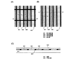
異なる複数の着色層と、遮光部とを有する半導体装置であって、
前記遮光部は、前記異なる複数の着色層から選ばれた複数の積層からなることを特徴とする。
ソース信号線と、ゲート信号線と、TFTと、
異なる複数の着色層と、遮光部とを有する半導体装置であって、
前記遮光部は、少なくとも前記ソース信号線と、前記ゲート信号線と、前記TFTとが形成される領域と重なって形成されていることを特徴とする。
複数の画素電極と、異なる複数の着色層と、
前記異なる複数の着色層から選ばれた複数の積層からなる遮光部とを有する半導体装置であって、
前記遮光部は、ある任意の画素電極と、当該画素電極に隣接する画素電極との間に形成されていることを特徴とする。
前記異なる複数の遮光部と、前記遮光部とは、いずれも対向基板上に形成されていることを特徴とする。
前記半導体装置は、自発光型の素子を用いた表示装置であることを特徴とする。
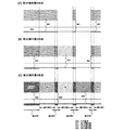
このときレジストからなるマスクと第2の導電層908bとがマスクとなり、第2のドーピング処理により、ゲート電極と重ならない第2の不純物領域(n-領域)907と、ゲート電極の一部と重なる第3の不純物領域(n--領域)909が形成される。第2の不純物領域907には1×10¹⁶〜1×10¹⁷/cm3の濃度範囲でn型を付与する不純物元素が添加される。
Claims (8)
- 第1の基板と、前記第1の基板に対向して設けられる第2の基板とを有し、
前記第1の基板上に、第1の画素と、前記第1の画素と隣接する第2の画素と、前記第2の画素と隣接する第3の画素と、ダミー画素とを有し、
前記第1の画素、前記第2の画素および前記第3の画素はそれぞれ、第1の電極、前記第1の電極の端部を覆うように設けられる絶縁膜、前記第1の電極および前記絶縁膜上に設けられる発光層、および前記発光層上に設けられる第2の電極でなる発光素子を有し、
前記第2の基板上に、前記第1の画素から発光された光が透過する第1の着色層と、前記第2の画素から発光された光が透過する第2の着色層と、前記第3の画素から発光された光が透過する第3の着色層と、前記第1の着色層の一部および前記第2の着色層の一部が重なって設けられる第1の遮光部と、前記第2の着色層の一部および前記第3の着色層の一部が重なって設けられる第2の遮光部と、前記第1の着色層の一部、前記第2の着色層の一部および前記第3の着色層の一部が重なって設けられる第3の遮光部を有し、
前記第1の遮光部は、隣接する前記第1の画素と前記第2の画素との間と重なり、
前記第2の遮光部は、隣接する前記第2の画素と前記第3の画素との間と重なり、
前記3の遮光部は、前記ダミー画素の発光領域と重なり、
前記絶縁膜は、前記第1の遮光部および前記第2の遮光部と重なる位置に設けられることを特徴とするEL表示装置。 - 請求項1において、
前記第1の画素の発光層、前記第2の画素の発光層および前記第3の画素の発光層は、同じ層で設けられていることを特徴とするEL表示装置。 - 請求項1または請求項2において、
前記第1の画素、前記第2の画素および前記第3の画素は、TFTを有することを特徴とするEL表示装置。 - 請求項1乃至請求項3のいずれか一項において、
前記第1の着色層、前記第2の着色層および前記第3の着色層上に、平坦化された保護膜を有することを特徴とするEL表示装置。 - 請求項4において、
前記保護膜の膜厚は、2μm〜3μmであることを特徴とするEL表示装置。 - 請求項1乃至請求項5のいずれか一項において、
前記絶縁膜は、感光性の有機樹脂であることを特徴とするEL表示装置。 - 請求項6において、
前記有機樹脂は、アクリルであることを特徴とするEL表示装置。 - 請求項1乃至請求項7のいずれか一項において、
前記絶縁膜は、窒化アルミニウム膜、窒化酸化アルミニウム膜、または窒化珪素膜からなる保護膜で覆われることを特徴とするEL表示装置。
Priority Applications (1)
| Application Number | Priority Date | Filing Date | Title |
|---|---|---|---|
| JP2003290913A JP4651922B2 (ja) | 2002-08-09 | 2003-08-08 | El表示装置 |
Applications Claiming Priority (2)
| Application Number | Priority Date | Filing Date | Title |
|---|---|---|---|
| JP2002233953 | 2002-08-09 | ||
| JP2003290913A JP4651922B2 (ja) | 2002-08-09 | 2003-08-08 | El表示装置 |
Publications (3)
| Publication Number | Publication Date |
|---|---|
| JP2004094236A JP2004094236A (ja) | 2004-03-25 |
| JP2004094236A5 JP2004094236A5 (ja) | 2006-09-21 |
| JP4651922B2 true JP4651922B2 (ja) | 2011-03-16 |
Family
ID=32072379
Family Applications (1)
| Application Number | Title | Priority Date | Filing Date |
|---|---|---|---|
| JP2003290913A Expired - Fee Related JP4651922B2 (ja) | 2002-08-09 | 2003-08-08 | El表示装置 |
Country Status (1)
| Country | Link |
|---|---|
| JP (1) | JP4651922B2 (ja) |
Families Citing this family (17)
| Publication number | Priority date | Publication date | Assignee | Title |
|---|---|---|---|---|
| US7764012B2 (en) * | 2004-04-16 | 2010-07-27 | Semiconductor Energy Laboratory Co., Ltd | Light emitting device comprising reduced frame portion, manufacturing method with improve productivity thereof, and electronic apparatus |
| JP4239890B2 (ja) | 2004-04-26 | 2009-03-18 | セイコーエプソン株式会社 | 有機el装置、電子機器 |
| US8350466B2 (en) * | 2004-09-17 | 2013-01-08 | Semiconductor Energy Laboratory Co., Ltd. | Display device and manufacturing method thereof |
| JP4823651B2 (ja) * | 2004-11-30 | 2011-11-24 | 株式会社半導体エネルギー研究所 | 発光装置及びその作製方法 |
| JP5025123B2 (ja) * | 2004-12-03 | 2012-09-12 | 株式会社半導体エネルギー研究所 | 表示装置及び電子機器 |
| US7365494B2 (en) | 2004-12-03 | 2008-04-29 | Semiconductor Energy Laboratory Co., Ltd. | Display device and manufacturing method thereof |
| JP2006332019A (ja) * | 2005-04-28 | 2006-12-07 | Seiko Epson Corp | 有機エレクトロルミネッセンス装置、及び有機エレクトロルミネッセンス装置の製造方法 |
| KR101424784B1 (ko) | 2006-01-10 | 2014-07-31 | 가부시키가이샤 한도오따이 에네루기 켄큐쇼 | 표시장치 및 그의 제조방법 |
| JP4939919B2 (ja) * | 2006-01-10 | 2012-05-30 | 株式会社半導体エネルギー研究所 | 表示装置 |
| CN101743782A (zh) | 2007-09-19 | 2010-06-16 | 富士电机控股株式会社 | 色变换滤光片、以及色变换滤光片和有机el显示器的制造方法 |
| KR101811782B1 (ko) * | 2008-07-10 | 2018-01-25 | 가부시키가이샤 한도오따이 에네루기 켄큐쇼 | 발광장치 및 전자기기 |
| JP4912437B2 (ja) * | 2008-08-05 | 2012-04-11 | 三星モバイルディスプレイ株式會社 | 有機発光表示装置 |
| WO2011027661A1 (en) | 2009-09-04 | 2011-03-10 | Semiconductor Energy Laboratory Co., Ltd. | Light-emitting device and method for manufacturing the same |
| EP2485567B1 (en) | 2009-11-10 | 2013-05-29 | Panasonic Corporation | Organic electroluminescence display apparatus |
| JP5720887B2 (ja) * | 2011-03-30 | 2015-05-20 | ソニー株式会社 | 表示装置および電子機器 |
| JP6152674B2 (ja) * | 2013-03-22 | 2017-06-28 | 大日本印刷株式会社 | 有機エレクトロルミネッセンス表示装置 |
| TWI681559B (zh) | 2013-10-10 | 2020-01-01 | 日商精工愛普生股份有限公司 | 發光裝置及包含其之電子機器 |
Citations (8)
| Publication number | Priority date | Publication date | Assignee | Title |
|---|---|---|---|---|
| JPH0465098A (ja) * | 1990-07-02 | 1992-03-02 | Sharp Corp | 薄膜elパネル |
| WO1998040871A1 (fr) * | 1997-03-12 | 1998-09-17 | Seiko Epson Corporation | Circuit pixel, afficheur, et equipement electronique a dispositif photoemetteur commande par courant |
| JP2000029014A (ja) * | 1998-07-07 | 2000-01-28 | Sharp Corp | 液晶表示素子用カラーフィルタ基板及び液晶表示素子 |
| JP2000162635A (ja) * | 1998-01-30 | 2000-06-16 | Seiko Epson Corp | 電気光学装置及びその製造方法並びに電子機器 |
| JP2001223074A (ja) * | 2000-02-07 | 2001-08-17 | Futaba Corp | 有機エレクトロルミネッセンス素子及びその駆動方法 |
| JP2002023686A (ja) * | 2000-05-24 | 2002-01-23 | Eastman Kodak Co | 基準ピクセルを含む固体ディスプレイ |
| JP2002304155A (ja) * | 2001-01-29 | 2002-10-18 | Semiconductor Energy Lab Co Ltd | 発光装置 |
| JP2003234186A (ja) * | 2001-12-06 | 2003-08-22 | Sony Corp | 表示装置およびその製造方法 |
-
2003
- 2003-08-08 JP JP2003290913A patent/JP4651922B2/ja not_active Expired - Fee Related
Patent Citations (8)
| Publication number | Priority date | Publication date | Assignee | Title |
|---|---|---|---|---|
| JPH0465098A (ja) * | 1990-07-02 | 1992-03-02 | Sharp Corp | 薄膜elパネル |
| WO1998040871A1 (fr) * | 1997-03-12 | 1998-09-17 | Seiko Epson Corporation | Circuit pixel, afficheur, et equipement electronique a dispositif photoemetteur commande par courant |
| JP2000162635A (ja) * | 1998-01-30 | 2000-06-16 | Seiko Epson Corp | 電気光学装置及びその製造方法並びに電子機器 |
| JP2000029014A (ja) * | 1998-07-07 | 2000-01-28 | Sharp Corp | 液晶表示素子用カラーフィルタ基板及び液晶表示素子 |
| JP2001223074A (ja) * | 2000-02-07 | 2001-08-17 | Futaba Corp | 有機エレクトロルミネッセンス素子及びその駆動方法 |
| JP2002023686A (ja) * | 2000-05-24 | 2002-01-23 | Eastman Kodak Co | 基準ピクセルを含む固体ディスプレイ |
| JP2002304155A (ja) * | 2001-01-29 | 2002-10-18 | Semiconductor Energy Lab Co Ltd | 発光装置 |
| JP2003234186A (ja) * | 2001-12-06 | 2003-08-22 | Sony Corp | 表示装置およびその製造方法 |
Also Published As
| Publication number | Publication date |
|---|---|
| JP2004094236A (ja) | 2004-03-25 |
Similar Documents
| Publication | Publication Date | Title |
|---|---|---|
| US7329985B2 (en) | Semiconductor device and manufacturing method thereof | |
| US10714557B2 (en) | Substrate for display device and display device including the same | |
| JP6691190B2 (ja) | 発光装置 | |
| JP4651922B2 (ja) | El表示装置 | |
| US20170271415A1 (en) | Display device and driving method thereof | |
| KR100968512B1 (ko) | 발광장치 및 그의 제조방법 | |
| EP2216840B1 (en) | Organic light emitting diode display | |
| CN1729719B (zh) | 显示装置和显示装置的制作方法 | |
| US8951902B2 (en) | Methods of removing contaminant impurities during the manufacture of a thin film transistor by applying water in which ozone is dissolved | |
| US20050202602A1 (en) | Method of manufacturing a semiconductor device | |
| US7439111B2 (en) | Semiconductor device and manufacturing method thereof | |
| JP2002083689A (ja) | 発光装置 | |
| JP2005322633A (ja) | 発光装置、電子機器、およびテレビジョン装置 | |
| JP4704006B2 (ja) | 表示装置及びその作製方法、並びに電子機器 | |
| JP4974493B2 (ja) | 半導体装置及び電子機器 | |
| EP1890333A2 (en) | Display device and method of making the same | |
| KR20150057016A (ko) | 유기전계 발광소자 및 이의 제조 방법 | |
| JP4754795B2 (ja) | 表示装置及び表示装置の作製方法 | |
| JP4785339B2 (ja) | 表示装置の作製方法 | |
| JP4583797B2 (ja) | 半導体装置の作製方法 | |
| JP4387090B2 (ja) | 半導体装置の作製方法 | |
| JP2005129920A (ja) | 半導体装置の作製方法 | |
| JP4128428B2 (ja) | 半導体装置の作製方法 | |
| JP4954387B2 (ja) | 半導体装置の作製方法 | |
| KR100637166B1 (ko) | 평판표시장치의 제조방법 |
Legal Events
| Date | Code | Title | Description |
|---|---|---|---|
| A521 | Request for written amendment filed |
Free format text: JAPANESE INTERMEDIATE CODE: A523 Effective date: 20060807 |
|
| A621 | Written request for application examination |
Free format text: JAPANESE INTERMEDIATE CODE: A621 Effective date: 20060807 |
|
| A131 | Notification of reasons for refusal |
Free format text: JAPANESE INTERMEDIATE CODE: A131 Effective date: 20090929 |
|
| RD02 | Notification of acceptance of power of attorney |
Free format text: JAPANESE INTERMEDIATE CODE: A7422 Effective date: 20091005 |
|
| A521 | Request for written amendment filed |
Free format text: JAPANESE INTERMEDIATE CODE: A523 Effective date: 20091030 |
|
| A131 | Notification of reasons for refusal |
Free format text: JAPANESE INTERMEDIATE CODE: A131 Effective date: 20100803 |
|
| A521 | Request for written amendment filed |
Free format text: JAPANESE INTERMEDIATE CODE: A523 Effective date: 20100825 |
|
| A131 | Notification of reasons for refusal |
Free format text: JAPANESE INTERMEDIATE CODE: A131 Effective date: 20101005 |
|
| A521 | Request for written amendment filed |
Free format text: JAPANESE INTERMEDIATE CODE: A523 Effective date: 20101108 |
|
| TRDD | Decision of grant or rejection written | ||
| A01 | Written decision to grant a patent or to grant a registration (utility model) |
Free format text: JAPANESE INTERMEDIATE CODE: A01 Effective date: 20101214 |
|
| A01 | Written decision to grant a patent or to grant a registration (utility model) |
Free format text: JAPANESE INTERMEDIATE CODE: A01 |
|
| A61 | First payment of annual fees (during grant procedure) |
Free format text: JAPANESE INTERMEDIATE CODE: A61 Effective date: 20101215 |
|
| R150 | Certificate of patent or registration of utility model |
Ref document number: 4651922 Country of ref document: JP Free format text: JAPANESE INTERMEDIATE CODE: R150 Free format text: JAPANESE INTERMEDIATE CODE: R150 |
|
| FPAY | Renewal fee payment (event date is renewal date of database) |
Free format text: PAYMENT UNTIL: 20131224 Year of fee payment: 3 |
|
| FPAY | Renewal fee payment (event date is renewal date of database) |
Free format text: PAYMENT UNTIL: 20131224 Year of fee payment: 3 |
|
| R250 | Receipt of annual fees |
Free format text: JAPANESE INTERMEDIATE CODE: R250 |
|
| R250 | Receipt of annual fees |
Free format text: JAPANESE INTERMEDIATE CODE: R250 |
|
| R250 | Receipt of annual fees |
Free format text: JAPANESE INTERMEDIATE CODE: R250 |
|
| R250 | Receipt of annual fees |
Free format text: JAPANESE INTERMEDIATE CODE: R250 |
|
| R250 | Receipt of annual fees |
Free format text: JAPANESE INTERMEDIATE CODE: R250 |
|
| R250 | Receipt of annual fees |
Free format text: JAPANESE INTERMEDIATE CODE: R250 |
|
| R250 | Receipt of annual fees |
Free format text: JAPANESE INTERMEDIATE CODE: R250 |
|
| R250 | Receipt of annual fees |
Free format text: JAPANESE INTERMEDIATE CODE: R250 |
|
| R250 | Receipt of annual fees |
Free format text: JAPANESE INTERMEDIATE CODE: R250 |
|
| LAPS | Cancellation because of no payment of annual fees |