JP4651922B2 - EL display device - Google Patents
EL display device Download PDFInfo
- Publication number
- JP4651922B2 JP4651922B2 JP2003290913A JP2003290913A JP4651922B2 JP 4651922 B2 JP4651922 B2 JP 4651922B2 JP 2003290913 A JP2003290913 A JP 2003290913A JP 2003290913 A JP2003290913 A JP 2003290913A JP 4651922 B2 JP4651922 B2 JP 4651922B2
- Authority
- JP
- Japan
- Prior art keywords
- pixel
- film
- layer
- light
- colored layer
- Prior art date
- Legal status (The legal status is an assumption and is not a legal conclusion. Google has not performed a legal analysis and makes no representation as to the accuracy of the status listed.)
- Expired - Fee Related
Links
- 239000000758 substrate Substances 0.000 claims description 47
- 230000001681 protective effect Effects 0.000 claims description 9
- 229910052581 Si3N4 Inorganic materials 0.000 claims description 7
- HQVNEWCFYHHQES-UHFFFAOYSA-N silicon nitride Chemical compound N12[Si]34N5[Si]62N3[Si]51N64 HQVNEWCFYHHQES-UHFFFAOYSA-N 0.000 claims description 7
- PMHQVHHXPFUNSP-UHFFFAOYSA-M copper(1+);methylsulfanylmethane;bromide Chemical compound Br[Cu].CSC PMHQVHHXPFUNSP-UHFFFAOYSA-M 0.000 claims description 5
- 239000011347 resin Substances 0.000 claims description 4
- 229920005989 resin Polymers 0.000 claims description 4
- NIXOWILDQLNWCW-UHFFFAOYSA-N acrylic acid group Chemical group C(C=C)(=O)O NIXOWILDQLNWCW-UHFFFAOYSA-N 0.000 claims description 3
- 238000009413 insulation Methods 0.000 claims 1
- 239000010408 film Substances 0.000 description 149
- 239000010410 layer Substances 0.000 description 147
- 239000012535 impurity Substances 0.000 description 41
- 238000000034 method Methods 0.000 description 41
- 239000004065 semiconductor Substances 0.000 description 32
- 238000005530 etching Methods 0.000 description 26
- 239000000463 material Substances 0.000 description 26
- 230000008569 process Effects 0.000 description 16
- 239000007789 gas Substances 0.000 description 14
- XUIMIQQOPSSXEZ-UHFFFAOYSA-N Silicon Chemical compound [Si] XUIMIQQOPSSXEZ-UHFFFAOYSA-N 0.000 description 12
- 230000015572 biosynthetic process Effects 0.000 description 12
- 229910052710 silicon Inorganic materials 0.000 description 12
- 239000010703 silicon Substances 0.000 description 12
- 239000010936 titanium Substances 0.000 description 11
- 239000012212 insulator Substances 0.000 description 10
- 238000002834 transmittance Methods 0.000 description 10
- 238000004519 manufacturing process Methods 0.000 description 8
- 239000011159 matrix material Substances 0.000 description 8
- 239000000956 alloy Substances 0.000 description 7
- 238000010438 heat treatment Methods 0.000 description 7
- VYPSYNLAJGMNEJ-UHFFFAOYSA-N silicon dioxide Inorganic materials O=[Si]=O VYPSYNLAJGMNEJ-UHFFFAOYSA-N 0.000 description 7
- 229910045601 alloy Inorganic materials 0.000 description 6
- 239000000460 chlorine Substances 0.000 description 6
- 239000004973 liquid crystal related substance Substances 0.000 description 6
- 229910052751 metal Inorganic materials 0.000 description 6
- 239000002184 metal Substances 0.000 description 6
- 238000005268 plasma chemical vapour deposition Methods 0.000 description 6
- 229910052719 titanium Inorganic materials 0.000 description 6
- 229910052721 tungsten Inorganic materials 0.000 description 6
- OAICVXFJPJFONN-UHFFFAOYSA-N Phosphorus Chemical compound [P] OAICVXFJPJFONN-UHFFFAOYSA-N 0.000 description 5
- RTAQQCXQSZGOHL-UHFFFAOYSA-N Titanium Chemical compound [Ti] RTAQQCXQSZGOHL-UHFFFAOYSA-N 0.000 description 5
- 239000003990 capacitor Substances 0.000 description 5
- 238000002425 crystallisation Methods 0.000 description 5
- 239000011229 interlayer Substances 0.000 description 5
- 229910052698 phosphorus Inorganic materials 0.000 description 5
- 239000011574 phosphorus Substances 0.000 description 5
- 238000000206 photolithography Methods 0.000 description 5
- 239000002356 single layer Substances 0.000 description 5
- 238000003860 storage Methods 0.000 description 5
- 239000010937 tungsten Substances 0.000 description 5
- 238000007740 vapor deposition Methods 0.000 description 5
- PXHVJJICTQNCMI-UHFFFAOYSA-N Nickel Chemical compound [Ni] PXHVJJICTQNCMI-UHFFFAOYSA-N 0.000 description 4
- 229920001609 Poly(3,4-ethylenedioxythiophene) Polymers 0.000 description 4
- 239000012298 atmosphere Substances 0.000 description 4
- 238000001704 evaporation Methods 0.000 description 4
- 230000008020 evaporation Effects 0.000 description 4
- 229910052739 hydrogen Inorganic materials 0.000 description 4
- 238000002161 passivation Methods 0.000 description 4
- 229910052814 silicon oxide Inorganic materials 0.000 description 4
- 239000002002 slurry Substances 0.000 description 4
- WFKWXMTUELFFGS-UHFFFAOYSA-N tungsten Chemical compound [W] WFKWXMTUELFFGS-UHFFFAOYSA-N 0.000 description 4
- NRTOMJZYCJJWKI-UHFFFAOYSA-N Titanium nitride Chemical compound [Ti]#N NRTOMJZYCJJWKI-UHFFFAOYSA-N 0.000 description 3
- 235000010724 Wisteria floribunda Nutrition 0.000 description 3
- 230000004913 activation Effects 0.000 description 3
- 229910052782 aluminium Inorganic materials 0.000 description 3
- XAGFODPZIPBFFR-UHFFFAOYSA-N aluminium Chemical compound [Al] XAGFODPZIPBFFR-UHFFFAOYSA-N 0.000 description 3
- 230000004888 barrier function Effects 0.000 description 3
- 239000004020 conductor Substances 0.000 description 3
- 230000008025 crystallization Effects 0.000 description 3
- 238000000151 deposition Methods 0.000 description 3
- 230000008021 deposition Effects 0.000 description 3
- 238000002347 injection Methods 0.000 description 3
- 239000007924 injection Substances 0.000 description 3
- 150000002500 ions Chemical class 0.000 description 3
- 230000010355 oscillation Effects 0.000 description 3
- 229910052760 oxygen Inorganic materials 0.000 description 3
- 238000000059 patterning Methods 0.000 description 3
- 239000000565 sealant Substances 0.000 description 3
- 239000010409 thin film Substances 0.000 description 3
- 229910000838 Al alloy Inorganic materials 0.000 description 2
- ZOXJGFHDIHLPTG-UHFFFAOYSA-N Boron Chemical compound [B] ZOXJGFHDIHLPTG-UHFFFAOYSA-N 0.000 description 2
- KRHYYFGTRYWZRS-UHFFFAOYSA-N Fluorane Chemical compound F KRHYYFGTRYWZRS-UHFFFAOYSA-N 0.000 description 2
- UFHFLCQGNIYNRP-UHFFFAOYSA-N Hydrogen Chemical compound [H][H] UFHFLCQGNIYNRP-UHFFFAOYSA-N 0.000 description 2
- CBENFWSGALASAD-UHFFFAOYSA-N Ozone Chemical compound [O-][O+]=O CBENFWSGALASAD-UHFFFAOYSA-N 0.000 description 2
- 239000004372 Polyvinyl alcohol Substances 0.000 description 2
- 229910000676 Si alloy Inorganic materials 0.000 description 2
- 229910052796 boron Inorganic materials 0.000 description 2
- 239000003054 catalyst Substances 0.000 description 2
- 238000000576 coating method Methods 0.000 description 2
- 239000003086 colorant Substances 0.000 description 2
- 238000011109 contamination Methods 0.000 description 2
- 238000009792 diffusion process Methods 0.000 description 2
- 238000001312 dry etching Methods 0.000 description 2
- 239000000428 dust Substances 0.000 description 2
- 239000011521 glass Substances 0.000 description 2
- 239000001257 hydrogen Substances 0.000 description 2
- AMWRITDGCCNYAT-UHFFFAOYSA-L hydroxy(oxo)manganese;manganese Chemical compound [Mn].O[Mn]=O.O[Mn]=O AMWRITDGCCNYAT-UHFFFAOYSA-L 0.000 description 2
- AMGQUBHHOARCQH-UHFFFAOYSA-N indium;oxotin Chemical compound [In].[Sn]=O AMGQUBHHOARCQH-UHFFFAOYSA-N 0.000 description 2
- 238000009616 inductively coupled plasma Methods 0.000 description 2
- 238000005468 ion implantation Methods 0.000 description 2
- 238000005499 laser crystallization Methods 0.000 description 2
- 238000005259 measurement Methods 0.000 description 2
- 229910052750 molybdenum Inorganic materials 0.000 description 2
- 229910052759 nickel Inorganic materials 0.000 description 2
- 150000002894 organic compounds Chemical class 0.000 description 2
- 238000005192 partition Methods 0.000 description 2
- 238000005498 polishing Methods 0.000 description 2
- 229920002451 polyvinyl alcohol Polymers 0.000 description 2
- -1 tungsten nitride Chemical class 0.000 description 2
- YVTHLONGBIQYBO-UHFFFAOYSA-N zinc indium(3+) oxygen(2-) Chemical compound [O--].[Zn++].[In+3] YVTHLONGBIQYBO-UHFFFAOYSA-N 0.000 description 2
- XLOMVQKBTHCTTD-UHFFFAOYSA-N zinc oxide Inorganic materials [Zn]=O XLOMVQKBTHCTTD-UHFFFAOYSA-N 0.000 description 2
- 229910018072 Al 2 O 3 Inorganic materials 0.000 description 1
- ZAMOUSCENKQFHK-UHFFFAOYSA-N Chlorine atom Chemical compound [Cl] ZAMOUSCENKQFHK-UHFFFAOYSA-N 0.000 description 1
- VYZAMTAEIAYCRO-UHFFFAOYSA-N Chromium Chemical compound [Cr] VYZAMTAEIAYCRO-UHFFFAOYSA-N 0.000 description 1
- YCKRFDGAMUMZLT-UHFFFAOYSA-N Fluorine atom Chemical compound [F] YCKRFDGAMUMZLT-UHFFFAOYSA-N 0.000 description 1
- ZOKXTWBITQBERF-UHFFFAOYSA-N Molybdenum Chemical compound [Mo] ZOKXTWBITQBERF-UHFFFAOYSA-N 0.000 description 1
- XYFCBTPGUUZFHI-UHFFFAOYSA-N Phosphine Chemical compound P XYFCBTPGUUZFHI-UHFFFAOYSA-N 0.000 description 1
- 229910003902 SiCl 4 Inorganic materials 0.000 description 1
- 229910004298 SiO 2 Inorganic materials 0.000 description 1
- 229910000577 Silicon-germanium Inorganic materials 0.000 description 1
- LEVVHYCKPQWKOP-UHFFFAOYSA-N [Si].[Ge] Chemical compound [Si].[Ge] LEVVHYCKPQWKOP-UHFFFAOYSA-N 0.000 description 1
- 230000001133 acceleration Effects 0.000 description 1
- UQZIWOQVLUASCR-UHFFFAOYSA-N alumane;titanium Chemical compound [AlH3].[Ti] UQZIWOQVLUASCR-UHFFFAOYSA-N 0.000 description 1
- CSDREXVUYHZDNP-UHFFFAOYSA-N alumanylidynesilicon Chemical compound [Al].[Si] CSDREXVUYHZDNP-UHFFFAOYSA-N 0.000 description 1
- PNEYBMLMFCGWSK-UHFFFAOYSA-N aluminium oxide Inorganic materials [O-2].[O-2].[O-2].[Al+3].[Al+3] PNEYBMLMFCGWSK-UHFFFAOYSA-N 0.000 description 1
- 239000005407 aluminoborosilicate glass Substances 0.000 description 1
- 150000004984 aromatic diamines Chemical class 0.000 description 1
- 229910052785 arsenic Inorganic materials 0.000 description 1
- RQNWIZPPADIBDY-UHFFFAOYSA-N arsenic atom Chemical compound [As] RQNWIZPPADIBDY-UHFFFAOYSA-N 0.000 description 1
- QVGXLLKOCUKJST-UHFFFAOYSA-N atomic oxygen Chemical compound [O] QVGXLLKOCUKJST-UHFFFAOYSA-N 0.000 description 1
- 229910052788 barium Inorganic materials 0.000 description 1
- DSAJWYNOEDNPEQ-UHFFFAOYSA-N barium atom Chemical compound [Ba] DSAJWYNOEDNPEQ-UHFFFAOYSA-N 0.000 description 1
- 230000000903 blocking effect Effects 0.000 description 1
- 239000005388 borosilicate glass Substances 0.000 description 1
- 238000006243 chemical reaction Methods 0.000 description 1
- 229910052801 chlorine Inorganic materials 0.000 description 1
- 229910052804 chromium Inorganic materials 0.000 description 1
- 239000011651 chromium Substances 0.000 description 1
- 239000011248 coating agent Substances 0.000 description 1
- 150000001875 compounds Chemical class 0.000 description 1
- 239000000356 contaminant Substances 0.000 description 1
- 238000001816 cooling Methods 0.000 description 1
- 229910052802 copper Inorganic materials 0.000 description 1
- 239000002274 desiccant Substances 0.000 description 1
- 230000006866 deterioration Effects 0.000 description 1
- 238000010586 diagram Methods 0.000 description 1
- 238000007865 diluting Methods 0.000 description 1
- 238000005401 electroluminescence Methods 0.000 description 1
- 230000001747 exhibiting effect Effects 0.000 description 1
- 238000000605 extraction Methods 0.000 description 1
- 229910052731 fluorine Inorganic materials 0.000 description 1
- 239000011737 fluorine Substances 0.000 description 1
- 230000005525 hole transport Effects 0.000 description 1
- 238000005984 hydrogenation reaction Methods 0.000 description 1
- 230000006872 improvement Effects 0.000 description 1
- 229910010272 inorganic material Inorganic materials 0.000 description 1
- 239000011147 inorganic material Substances 0.000 description 1
- 230000001678 irradiating effect Effects 0.000 description 1
- 238000010030 laminating Methods 0.000 description 1
- 238000003475 lamination Methods 0.000 description 1
- 238000004518 low pressure chemical vapour deposition Methods 0.000 description 1
- 238000012423 maintenance Methods 0.000 description 1
- 239000011572 manganese Substances 0.000 description 1
- 239000012528 membrane Substances 0.000 description 1
- 239000000203 mixture Substances 0.000 description 1
- 239000011733 molybdenum Substances 0.000 description 1
- VOFUROIFQGPCGE-UHFFFAOYSA-N nile red Chemical compound C1=CC=C2C3=NC4=CC=C(N(CC)CC)C=C4OC3=CC(=O)C2=C1 VOFUROIFQGPCGE-UHFFFAOYSA-N 0.000 description 1
- 229910052757 nitrogen Inorganic materials 0.000 description 1
- 239000012299 nitrogen atmosphere Substances 0.000 description 1
- 230000003287 optical effect Effects 0.000 description 1
- 239000001301 oxygen Substances 0.000 description 1
- 230000035699 permeability Effects 0.000 description 1
- 239000000049 pigment Substances 0.000 description 1
- 238000002294 plasma sputter deposition Methods 0.000 description 1
- 229920003023 plastic Polymers 0.000 description 1
- 239000004033 plastic Substances 0.000 description 1
- 229910021420 polycrystalline silicon Inorganic materials 0.000 description 1
- 239000002861 polymer material Substances 0.000 description 1
- 239000000843 powder Substances 0.000 description 1
- 239000010453 quartz Substances 0.000 description 1
- 239000012495 reaction gas Substances 0.000 description 1
- 230000009467 reduction Effects 0.000 description 1
- 230000004044 response Effects 0.000 description 1
- 238000007789 sealing Methods 0.000 description 1
- 239000000377 silicon dioxide Substances 0.000 description 1
- 238000004528 spin coating Methods 0.000 description 1
- 238000004544 sputter deposition Methods 0.000 description 1
- 239000000126 substance Substances 0.000 description 1
- 229910052715 tantalum Inorganic materials 0.000 description 1
- MZLGASXMSKOWSE-UHFFFAOYSA-N tantalum nitride Chemical compound [Ta]#N MZLGASXMSKOWSE-UHFFFAOYSA-N 0.000 description 1
- MTPVUVINMAGMJL-UHFFFAOYSA-N trimethyl(1,1,2,2,2-pentafluoroethyl)silane Chemical compound C[Si](C)(C)C(F)(F)C(F)(F)F MTPVUVINMAGMJL-UHFFFAOYSA-N 0.000 description 1
- XLYOFNOQVPJJNP-UHFFFAOYSA-N water Substances O XLYOFNOQVPJJNP-UHFFFAOYSA-N 0.000 description 1
- 238000001039 wet etching Methods 0.000 description 1
- 239000011787 zinc oxide Substances 0.000 description 1
- ZVWKZXLXHLZXLS-UHFFFAOYSA-N zirconium nitride Chemical compound [Zr]#N ZVWKZXLXHLZXLS-UHFFFAOYSA-N 0.000 description 1
Images


Classifications
-
- H—ELECTRICITY
- H10—SEMICONDUCTOR DEVICES; ELECTRIC SOLID-STATE DEVICES NOT OTHERWISE PROVIDED FOR
- H10K—ORGANIC ELECTRIC SOLID-STATE DEVICES
- H10K59/00—Integrated devices, or assemblies of multiple devices, comprising at least one organic light-emitting element covered by group H10K50/00
- H10K59/30—Devices specially adapted for multicolour light emission
- H10K59/38—Devices specially adapted for multicolour light emission comprising colour filters or colour changing media [CCM]
-
- H—ELECTRICITY
- H10—SEMICONDUCTOR DEVICES; ELECTRIC SOLID-STATE DEVICES NOT OTHERWISE PROVIDED FOR
- H10K—ORGANIC ELECTRIC SOLID-STATE DEVICES
- H10K59/00—Integrated devices, or assemblies of multiple devices, comprising at least one organic light-emitting element covered by group H10K50/00
- H10K59/80—Constructional details
- H10K59/8791—Arrangements for improving contrast, e.g. preventing reflection of ambient light
- H10K59/8792—Arrangements for improving contrast, e.g. preventing reflection of ambient light comprising light absorbing layers, e.g. black layers
Landscapes
- Electroluminescent Light Sources (AREA)
- Devices For Indicating Variable Information By Combining Individual Elements (AREA)
- Thin Film Transistor (AREA)
Description
本発明は、薄膜トランジスタ(以下、TFTと表記する)で構成された回路を有する半導体装置およびその作製方法に関する。 The present invention relates to a semiconductor device having a circuit including a thin film transistor (hereinafter referred to as TFT) and a manufacturing method thereof.
また、半導体装置とは、半導体特性を利用することで機能しうる装置全般を指し、液晶表示装置、エレクトロルミネッセンス(以下、ELと表記する)素子を代表とする自発光素子を有する表示装置(EL表示装置)、半導体回路およびそれらを部品として用いた電子機器等は全て半導体装置に含まれるものとする。 Further, a semiconductor device refers to all devices that can function by utilizing semiconductor characteristics, and is a liquid crystal display device, a display device (EL) represented by an electroluminescence (hereinafter referred to as EL) element (EL) Display devices), semiconductor circuits, and electronic devices using them as components are all included in the semiconductor device.
近年、絶縁表面を有する基板上に形成された半導体薄膜(厚さ数nm〜数百nm程度)を用いてTFTを構成する技術が注目されている。TFTは電子デバイスに広く応用が期待され、特に液晶表示装置、EL表示装置を駆動するためのスイッチング素子として開発が急がれている。 2. Description of the Related Art In recent years, attention has been focused on a technique for forming a TFT using a semiconductor thin film (having a thickness of several nm to several hundred nm) formed on a substrate having an insulating surface. TFTs are expected to be widely applied to electronic devices, and in particular, the development of switching elements for driving liquid crystal display devices and EL display devices is urgently needed.
表示装置において、高品質な画質を得るために、画素電極をマトリクス状に配置し、画素電極の各々に接続されたスイッチング素子を駆動することによって表示を行うアクティブマトリクス型表示装置が注目を集めている。中でも、液晶表示装置に代わり、自発光型の素子であるEL素子を用いた画素を有するEL表示装置は、次世代のディスプレイ装置としての期待が集まっている。 In a display device, in order to obtain high quality image quality, an active matrix type display device that performs display by arranging pixel electrodes in a matrix and driving a switching element connected to each pixel electrode attracts attention. Yes. In particular, an EL display device including a pixel using an EL element which is a self-luminous element instead of a liquid crystal display device has been expected as a next-generation display device.
EL表示装置は、第1の電極と第2の電極間に挟まれるように形成されたEL層を有し、前記第1および第2の電極間に電流が生じて発光を得、それによって画像の表示を行う表示装置である。その利点として、液晶表示装置のようなバックライトを必要としないことによるデバイスの軽薄短小化、広視野角、応答速度の速さによる動画表示の滑らかさ等が挙げられる。 The EL display device has an EL layer formed so as to be sandwiched between a first electrode and a second electrode, and a current is generated between the first and second electrodes to obtain light emission, whereby an image is obtained. It is a display apparatus which displays. Advantages include light and thin devices due to the absence of a backlight like a liquid crystal display device, wide viewing angle, smoothness of moving image display due to high response speed, and the like.
EL表示装置において、カラー表示を実現する方法としては、赤(R)、緑(G)、青(B)それぞれの発光色を呈するEL材料を用いて、各々の発光部を形成する方法と、白色あるいは青色等の単色発光のEL材料を用い、その出射光をカラーフィルタあるいは色変換層を通すことによってRGBそれぞれの発光を得る方法とがある。 In the EL display device, as a method of realizing color display, a method of forming each light emitting portion using EL materials exhibiting red (R), green (G), and blue (B) emission colors, and There is a method of obtaining light emission of each of RGB by using an EL material that emits monochromatic light such as white or blue and passing the emitted light through a color filter or a color conversion layer.
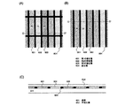
ここで、一般に表示装置に用いるカラーフィルタは、図6(A)〜(C)に示すように、R、G、Bそれぞれの着色層601〜603と、遮光層604とを有し、着色層に照射された光の一部を吸収し、一部を透過することによってR、G、Bの光を抽出する。また、遮光層604は一般的に金属膜(クロム等)または黒色顔料を含有した有機膜等で形成されている。遮光層604は、図6(A)のように隣接する画素間の上下左右に設けられていても良いし、図6(B)のようにストライプ状に設けられていても良い。また、画素配置がデルタ配置である場合等はこの限りでない。
Here, as shown in FIGS. 6A to 6C, a color filter generally used in a display device includes R, G, and B colored
図6(A)(B)において、D−D'間の断面を図6(C)に示す。基板651上に遮光層604、着色層601〜603を形成した後、表面を平坦化するため、平坦化膜652を設けても良い。さらにこの平坦化膜652は、着色層601〜603に含まれる不純物のバリア層として用いることも可能である。
6A and 6B, a cross section between DD ′ is shown in FIG. After the
また、EL素子からの出射光の取り出し方向によって、図4(A)に示すように、TFTが形成されている基板側から取り出すものを下面出射、逆に、図4(B)に示すように、対向基板側から取り出すものを上面出射という。 Further, as shown in FIG. 4 (A), the light extracted from the substrate side on which the TFT is formed is emitted from the bottom surface depending on the extraction direction of the emitted light from the EL element, and conversely, as shown in FIG. 4 (B). What is taken out from the counter substrate side is called top emission.
カラーフィルタを形成する場合、出射光の取り出し方向によって、形成する位置が異なる。下面出射の場合、カラーフィルタは、図4(A)に示したとおり、画素電極410よりもTFT基板400に近い側に着色層を設けることによって形成する必要がある。つまり、TFT形成→配線形成→着色層形成→画素電極形成→EL層形成→対向電極形成→対向基板による封止という工程になる。状面出射の場合、出射光は対向電極側から得られるので、カラーフィルタは、図4(B)に示したとおり、対向基板側に着色層を設けることによって形成される。つまり、TFT基板側の工程とは独立して形成される。
When forming the color filter, the position to be formed differs depending on the direction of outgoing light. In the case of bottom emission, the color filter needs to be formed by providing a colored layer closer to the
下面出射の場合のように、TFT基板側でカラーフィルタを形成すると、後工程での熱処理温度に着色層自体が耐えられないため、以降のプロセス温度を低くする必要がある、また、熱によって着色層内の不純物が拡散することによってTFTが汚染されるといった問題がある。よって図4(A)に示すように、着色層形成部の上下は、窒化シリコン膜等を代表とするバリア層を設ける必要がある。反面、上面出射の場合は、TFT基板形成の工程と独立してカラーフィルタが形成出来るため、前述の心配の必要がない点で適しているといえる。 If the color filter is formed on the TFT substrate side as in the case of bottom emission, the colored layer itself cannot withstand the heat treatment temperature in the subsequent process, so that it is necessary to lower the subsequent process temperature. There is a problem that the TFT is contaminated by the diffusion of impurities in the layer. Therefore, as shown in FIG. 4A, a barrier layer typified by a silicon nitride film or the like needs to be provided above and below the colored layer forming portion. On the other hand, in the case of top emission, it can be said that the color filter can be formed independently of the TFT substrate forming step, and therefore it is suitable in that the above-mentioned worry is not necessary.
ところで、EL表示装置の場合、EL層を形成する際、エッジ部分が表示エリアにかからないようにマージンを確保するため、表示エリアの外縁にはダミー画素を設けることが多い。 By the way, in the case of an EL display device, when forming an EL layer, a dummy pixel is often provided on the outer edge of the display area in order to ensure a margin so that the edge portion does not cover the display area.
また、表示エリア外に電流モニタ画素を設け、表示エリアの輝度ばらつき補正等を行う方法もあるが、このような場合には先のダミー画素の一部を電流モニタ画素として用いることがある(特許文献1参照)。 In addition, there is a method of providing a current monitor pixel outside the display area and correcting the luminance variation of the display area. In such a case, a part of the previous dummy pixel may be used as the current monitor pixel (patent). Reference 1).
このようなダミー画素、電流モニタ画素は、本来発光しない部分であるから、遮光層を形成して光漏れが起こらないようにする必要がある。ここで、EL表示装置が下面出射である場合、図2(A)に示すように、EL層202からの出射光が視認されるまでの経路には、配線、ゲート電極等、不透明材料で形成される部分が多いため、それらの材料を利用して遮光層204を形成することで、カラーフィルタ形成時に遮光層形成用のマスクを減らすことが可能である。
Since such dummy pixels and current monitor pixels are portions that do not emit light originally, it is necessary to form a light shielding layer to prevent light leakage. Here, when the EL display device emits light from the bottom, as shown in FIG. 2A, the path until the light emitted from the
一方、上面出射の場合、図2(B)に示すように、EL層252からの出射光が視認されるまでの経路に不透明材料で形成されるものを持たないため、別途遮光層254を形成する必要があるため、工程増加・歩留まり低下等が懸念される。
On the other hand, in the case of top emission, as shown in FIG. 2B, since there is no material formed of an opaque material in the path until the emitted light from the
本発明は前述の問題を鑑みてなされたものであり、マスク枚数を増加させることなく、高精度に遮光層を形成し、高品位な表示が得られる表示装置を提供することを目的とする。 The present invention has been made in view of the above-described problems, and an object of the present invention is to provide a display device in which a light shielding layer is formed with high accuracy and a high-quality display can be obtained without increasing the number of masks.
一般的に可視光と言われているものは、その波長が400nm〜780nm程度の光を指す。カラーフィルタに用いられる着色層は、この可視光のうち、ある特定の領域の波長を有する光のみを透過することによって着色光を提供するものであり、異なる色の着色層は、当然ながら互いに異なる領域の波長を有する光を透過させる特性を有する。 What is generally called visible light refers to light having a wavelength of about 400 nm to 780 nm. The colored layer used in the color filter provides colored light by transmitting only light having a wavelength in a specific region out of the visible light, and the colored layers of different colors are naturally different from each other. It has a characteristic of transmitting light having a wavelength in the region.
つまり、ある着色層で高い透過率を有する波長の光であっても、異なる着色層においては殆ど透過されないことになる。本発明はこの点に着目し、遮光したい部位において、2層ないしは3層の着色層を積層形成することによって、前述の波長領域にある光をまんべんなく遮光することの出来る層を設けて遮光層とし、別途遮光層の形成を必要としないため、工程削減による製造コストの低下および歩留まり向上が実現できる。 That is, even light having a wavelength having high transmittance in a certain colored layer is hardly transmitted in different colored layers. The present invention pays attention to this point, and by forming two or three colored layers in a portion to be shielded from light, a layer capable of evenly shielding light in the aforementioned wavelength region is provided as a light shielding layer. In addition, since it is not necessary to form a separate light shielding layer, the manufacturing cost can be reduced and the yield can be improved by reducing the number of processes.
本発明の構成を以下に記す。 The configuration of the present invention will be described below.
本発明は、
異なる複数の着色層と、遮光部とを有する半導体装置であって、
前記遮光部は、前記異なる複数の着色層から選ばれた複数の積層からなることを特徴とする。
The present invention
A semiconductor device having a plurality of different colored layers and a light shielding portion,
The light-shielding portion is composed of a plurality of stacked layers selected from the plurality of different colored layers.
本発明は、
ソース信号線と、ゲート信号線と、TFTと、
異なる複数の着色層と、遮光部とを有する半導体装置であって、
前記遮光部は、少なくとも前記ソース信号線と、前記ゲート信号線と、前記TFTとが形成される領域と重なって形成されていることを特徴とする。
The present invention
A source signal line, a gate signal line, a TFT,
A semiconductor device having a plurality of different colored layers and a light shielding portion,
The light shielding portion is formed to overlap at least a region where the source signal line, the gate signal line, and the TFT are formed.
本発明は、
複数の画素電極と、異なる複数の着色層と、
前記異なる複数の着色層から選ばれた複数の積層からなる遮光部とを有する半導体装置であって、
前記遮光部は、ある任意の画素電極と、当該画素電極に隣接する画素電極との間に形成されていることを特徴とする。
The present invention
A plurality of pixel electrodes, a plurality of different colored layers,
A semiconductor device having a light-shielding portion composed of a plurality of laminated layers selected from the plurality of different colored layers,
The light-shielding portion is formed between an arbitrary pixel electrode and a pixel electrode adjacent to the pixel electrode.
本発明においては、
前記異なる複数の遮光部と、前記遮光部とは、いずれも対向基板上に形成されていることを特徴とする。
In the present invention,
The plurality of different light-shielding portions and the light-shielding portion are all formed on a counter substrate.
本発明においては、
前記半導体装置は、自発光型の素子を用いた表示装置であることを特徴とする。
In the present invention,
The semiconductor device is a display device using a self-luminous element.
本発明では、異なる複数の着色層の積層膜によって遮光部を形成する。結果として、遮光層(ブラックマトリクス)の形成工程を削減し、製造コスト低減、歩留まりの向上に寄与する。 In the present invention, the light shielding portion is formed by a laminated film of a plurality of different colored layers. As a result, the formation process of the light shielding layer (black matrix) is reduced, which contributes to a reduction in manufacturing cost and an improvement in yield.
図1に、本発明の実施形態を示す。図1(A)はEL表示装置の画素部であり、各画素はマトリクス状に配置され、それぞれ、ソース信号線101、第1のゲート信号線102、第2のゲート信号線103、電流供給線104、スイッチング用TFT105、消去用TFT106、駆動用TFT107、保持容量108、画素電極109を有する。保持容量108に関しては、定められた表示期間中、駆動用TFT107のゲート・ソース間電圧を正常に保持できるのであれば特に設けなくても良い。
FIG. 1 shows an embodiment of the present invention. FIG. 1A illustrates a pixel portion of an EL display device, in which each pixel is arranged in a matrix, and each includes a source signal line 101, a first
図1(A)において、A−A'間の断面を図1(B)に示す。基板151上にはそれぞれTFTが形成され、TFTの活性層の形成と同時に、保持容量の第1電極153が形成され、TFTのゲート電極の形成と同時に、保持容量の第2電極154が形成され、ゲート絶縁膜155を介して保持容量を形成している。さらに層間絶縁膜156を介して配線および画素電極157が形成され、さらに平坦化に優れた樹脂等を用いて絶縁層を形成し、発光部となる部分を開口して隔壁158が形成され、その後、EL層159および対向電極160が形成される。ここに示したEL表示装置は上面出射型であるので、画素電極157は反射率の高い材料を用い、対向電極160には透過率の高い材料を用いるのが望ましい。
In FIG. 1A, a cross section between AA ′ is shown in FIG. A TFT is formed on each of the
一方、対向基板152上には、第1〜第3の着色層が順次形成されてカラーフィルタとなる。画素部において、ダミー画素、電流モニタ画素等、出射光を取り出さない領域(図1(A)中、Dummyと表記されている列)においては、第1〜第3の着色層を2層ないしは3層積層することによって遮光層とする。さらに、特に図示していないが、着色層の上には、平坦化、着色層内の不純物の拡散防止のための保護膜を形成しても良い。
On the other hand, first to third colored layers are sequentially formed on the
また、隣接画素間の遮光層は、図1(B)においては隣接する着色層を2層積層して形成しているが、図7において点線丸枠で示すように、着色層を3層積層して形成しても良い。 In addition, the light shielding layer between adjacent pixels is formed by stacking two adjacent colored layers in FIG. 1B, but as shown by a dotted circle in FIG. 7, three colored layers are stacked. May be formed.
図3(A)に、着色層R+Bの2層積層膜、着色層B+Gの2層積層膜、着色層R+Gの2層積層膜のそれぞれにおける透過率を測定した結果を示す。この場合、積層膜の透過率は、およそ各着色層の透過率の積に等しい。着色層R+Bの2層積層膜においては、全領域で透過率は7%以下程度であり、おおむね良好な遮光特性を有しているが、着色層B+Gの2層積層膜、着色層R+Gの2層積層膜においては、ある波長域では数10%が透過している。 FIG. 3A shows the results of measuring the transmittance in each of the two-layer laminated film of the colored layer R + B, the two-layer laminated film of the colored layer B + G, and the two-layer laminated film of the colored layer R + G. In this case, the transmittance of the laminated film is approximately equal to the product of the transmittance of each colored layer. The two-layer laminated film of the colored layer R + B has a transmittance of about 7% or less in the entire region and generally has good light-shielding properties. However, the two-layer laminated film of the colored layer B + G and 2 of the colored layer R + G In the layer laminated film, several tens of percent are transmitted in a certain wavelength region.
また、図3(B)に、R、G、Bそれぞれの着色層の透過率の測定結果と、3層積層膜とした場合の透過率の積の計算結果を示す。3層積層膜とすることにより、透過率は全領域で4%以下程度となり、十分に遮光膜として機能するといえる。 FIG. 3B shows the measurement result of the transmittance of each of the colored layers of R, G, and B and the calculation result of the product of the transmittance when a three-layer laminated film is formed. By using a three-layered film, the transmittance is about 4% or less in the entire region, and it can be said that the film functions sufficiently as a light shielding film.
EL表示装置等においては、出射光の強度が大きいので、2層積層膜にて形成した遮光層では十分な遮光が実現しない可能性がある。よって、図7に示したように、3層積層膜を用いた遮光層とするのが望ましい。これは透過型液晶表示装置等においても同様である。一方、反射型液晶表示装置等においては、自然光を用いるためそれほど光強度が大きくない。このような場合、2層積層膜(中でも比較的遮光特性の良好なR+Bの2層積層膜、もしくはG+Bの2層積層膜が望ましい)を用いて遮光層としても良い。 In an EL display device or the like, since the intensity of emitted light is large, there is a possibility that sufficient light shielding may not be realized with a light shielding layer formed of a two-layer laminated film. Therefore, as shown in FIG. 7, it is desirable to use a light-shielding layer using a three-layer laminated film. The same applies to a transmissive liquid crystal display device or the like. On the other hand, in a reflective liquid crystal display device or the like, light intensity is not so high because natural light is used. In such a case, a light-shielding layer may be formed by using a two-layer laminated film (in particular, a R + B two-layer laminated film or a G + B two-layer laminated film having relatively good light-shielding characteristics).
またここでは例として、一般的なカラー表示に対応した、R、G、B3色の着色層を有する表示装置を対象として説明したが、例えば異なる2色、もしくは異なる4色以上の着色層を有し、多色表示が可能な表示装置においても同様の手法が適用出来ることは言うまでもない。 Further, here, as an example, a display device having three, R, G, and B colored layers corresponding to general color display has been described, but for example, there are two or more different colored layers. Needless to say, the same method can be applied to a display device capable of multicolor display.
まず、対向基板800には、コーニング社の#7059ガラスや#1737ガラス等に代表されるバリウムホウケイ酸ガラスやアルミノホウケイ酸ガラスを用いる。その他、石英基板、プラスチック基板等の透光性基板を用いることも出来る。
First, the
次いで、対向基板800上に有機感光性材料(CRY−S778:富士フィルムオーリン社製COLOR MOSAIC)を塗布し、フォトリソグラフィ法により、この有機感光性材料を図8(A)に示すようにパターニングして、第1の着色層(R)801を所定の位置に形成する。
Next, an organic photosensitive material (CRY-S778: COLOR MOSAIC manufactured by Fuji Film Orin Co., Ltd.) is applied on the
次いで、先のものとは異なる有機感光性材料(CGY−S705C:富士フィルムオーリン社製COLOR MOSAIC)を塗布し、フォトリソグラフィ法により、この有機感光性材料を図8(B)に示すようにパターニングして、第2の着色層(G)802を所定の位置に形成する。 Next, an organic photosensitive material (CGY-S705C: COLOR MOSAIC manufactured by Fuji Film Orin) different from the previous one is applied, and this organic photosensitive material is patterned by photolithography as shown in FIG. 8B. Then, the second colored layer (G) 802 is formed at a predetermined position.
さらに、先の2者とは異なる有機感光性材料(CVB−S706C:富士フィルムオーリン社製COLOR MOSAIC)を塗布し、フォトリソグラフィ法により、この有機感光性材料を図8(C)に示すようにパターニングして、第3の着色層(B)803を所定の位置に形成する。 Further, an organic photosensitive material (CVB-S706C: COLOR MOSAIC manufactured by Fuji Film Olin Co., Ltd.) different from the previous two is applied, and this organic photosensitive material is shown in FIG. 8C by photolithography. Patterning is performed to form the third colored layer (B) 803 at a predetermined position.
図8(C)に示すように、第1の着色層(R)801の一部は、遮光層1〜4において、第2の着色層(G)802の一部と、第3の着色層(B)803の一部と重なる。ここで、遮光部1は、ダミー画素および電流モニタ画素の発光部を遮光する領域であり、遮光部2〜4は、隣接画素間の光漏れを抑えるために形成される。第1の着色層(R)801において、第2、第3の着色層のいずれとも重なっていない領域が、開口部Rとなる。同じく、第2の着色層(G)802において、第1、第3の着色層とのいずれとも重なっていない領域が、開口部Gとなり、第3の着色層(B)803において、第1、第2の着色層のいずれとも重なっていない領域が、開口部Bとなる。
As shown in FIG. 8C, a part of the first colored layer (R) 801 is the same as the part of the second colored layer (G) 802 in the light shielding layers 1 to 4 and the third colored layer. (B) Overlaps part of 803. Here, the
以上で、3回のフォトリソグラフィ法によって、金属膜等による遮光層の形成工程を省略し、開口部と遮光部とを形成することが出来る。 As described above, the step of forming the light shielding layer using a metal film or the like can be omitted by three photolithography methods, and the opening and the light shielding portion can be formed.
必要な場合には、各着色層を覆う保護膜(図示せず)を形成する。着色層が単層である部分と、複数の着色層が重なっている部分とでは段差が生じるため、この保護膜を平坦化膜として用いても良い。この場合、2μm〜3μmの膜厚を必要とする。また、着色層内の不純物による汚染を防ぐ目的がある場合には、汚染物質のブロック性の高い膜を用いるのが望ましい。 If necessary, a protective film (not shown) that covers each colored layer is formed. Since a step is generated between a portion where the colored layer is a single layer and a portion where a plurality of colored layers overlap, this protective film may be used as a planarizing film. In this case, a film thickness of 2 μm to 3 μm is required. In addition, when there is a purpose of preventing contamination by impurities in the colored layer, it is desirable to use a film having a high blocking property of contaminants.
なお、本実施例においては、有機感光性材料を塗布して、フォトリソグラフィ法により所望の形状にパターニングして各着色層801〜803を形成したが、特に上記作製方法に限定されないことは言うまでもない。
In this example, an organic photosensitive material was applied and patterned into a desired shape by a photolithography method to form each of the
さらに、着色層801〜803の形成順序等に関しても、本実施例の限りではない。
Further, the order of forming the
本実施例においては、上面出射型のアクティブマトリクス型EL表示装置を作製した例について説明する。 In this embodiment, an example of manufacturing a top emission type active matrix EL display device will be described.
図5(A)は、本発明を適用して作製された、上面出射型のアクティブマトリクス型EL表示装置の外観を示している。基板500の中央部には、画素部502が設けられており、その周辺には、ソース信号線駆動回路503、第1のゲート信号線駆動回路504、第2のゲート信号線駆動回路505が設けられている。各駆動回路への電源供給および駆動信号入力は、外部回路より、フレキシブルプリント基板(FPC)506を介して行われる。
FIG. 5A shows the appearance of a top emission type active matrix EL display device manufactured by applying the present invention. A
図5(A)において、C−C'間の断面図を図5(B)に示す。基板500と、対向基板501とは、図5(B)に示すように、封止剤553によって、外周に沿って接着、固定され、画素部502に形成されたEL層が、外気に接触しないように密閉されている。さらに、封止剤を塗布した領域の内周に沿って、対向基板501には溝部が形成され、乾燥剤554が設けられ、水分によるEL層の劣化を抑制している。また、対向基板501には、実施形態および実施例1に従って、着色層552が形成されている。図5(B)では図示していないが、EL層およびTFTの、着色層内の不純物による汚染が心配される場合には、着色層の表面を覆うように保護膜を形成しても良い。
In FIG. 5A, a cross-sectional view along CC ′ is shown in FIG. As shown in FIG. 5B, the
FPC506と基板500の接続は、内部に導電性物質を含有した異方導電性ペースト551を用いて圧着、固定され、導電性物質によって、基板上の信号入出力用端子と導通している。
The connection between the
本実施例においては、基板上に形成されたTFTの作製方法について説明する。なお基板には複数のTFTが設けられているが、駆動回路部に形成されたnチャネル型TFT及びpチャネル型TFTと、画素部に形成されたnチャネル型TFTとpチャネル型TFTについて説明する。 In this embodiment, a method for manufacturing a TFT formed over a substrate will be described. Note that although a plurality of TFTs are provided on the substrate, an n-channel TFT and a p-channel TFT formed in the driver circuit portion, and an n-channel TFT and a p-channel TFT formed in the pixel portion will be described. .
まず、絶縁表面を有する基板901上に酸化シリコン膜、窒化シリコン膜または酸化窒化シリコン膜などの絶縁膜の積層からなる下地絶縁膜を形成する(図9には図示しない)。ここでは下地絶縁膜として2層構造を用いても、前記絶縁膜の単層膜または3層以上積層させた構造を用いても良い。下地絶縁膜の一層目としては、プラズマCVD法を用い、SiH4、NH3、N2O及びH2を反応ガスとして成膜される酸化窒化シリコン膜を10〜200nm(好ましくは50〜100nm)形成する。次いで、下地絶縁膜の二層目としては、プラズマCVD法を用い、SiH4及びN2Oを反応ガスとして成膜される酸化窒化シリコン膜を50〜200nm(好ましくは100〜150nm)の厚さに積層形成する。
First, a base insulating film formed of a stack of insulating films such as a silicon oxide film, a silicon nitride film, or a silicon oxynitride film is formed over a
次いで、図9(A)に示すように、下地絶縁膜上に半導体膜902を形成する。半導体膜は、非晶質構造を有する半導体膜を公知の手段(スパッタ法、LPCVD法、またはプラズマCVD法等)により成膜した後、結晶化処理(レーザー結晶化法、熱結晶化法、またはニッケルなどの触媒を用いた熱結晶化法等)を行う。また、ニッケルなどの触媒を用いた熱結晶化の後、レーザーを照射し、結晶化を促進すると好ましい。なお、半導体膜の材料に限定はないが、好ましくはシリコンまたはシリコンゲルマニウム合金などで形成すると良い。
Next, as illustrated in FIG. 9A, a
また、レーザー結晶化法で結晶質半導体膜を作製する場合には、パルス発振型または連続発光型のエキシマレーザーやYAGレーザー、YVO4レーザーを用いることができる。これらのレーザーを用いる場合には、レーザー発振器から放射されたレーザー光を光学系で線状に集光し半導体膜に照射する方法を用いると良い。結晶化の条件は実施者が適宣選択するものであるが、エキシマレーザーを用いる場合はパルス発振周波数30Hzとし、レーザーエネルギー密度を100〜400mJ/cm2(代表的には200〜300mJ/cm2)とする。また、YAGレーザーを用いる場合にはその第2高調波を用いパルス発振周波数1〜10kHzとし、レーザーエネルギー密度を300〜600mJ/cm2(代表的には350〜500mJ/cm2)とすると良い。そして幅100〜1000μm、例えば400μmで線状に集光したレーザー光を基板全面に渡って照射し、この時の線状レーザー光の重ね合わせ率(オーバーラップ率)を50〜98%として行えばよい。 When a crystalline semiconductor film is formed by a laser crystallization method, a pulse oscillation type or continuous emission type excimer laser, YAG laser, or YVO 4 laser can be used. When these lasers are used, it is preferable to use a method in which laser light emitted from a laser oscillator is linearly collected by an optical system and irradiated onto a semiconductor film. Crystallization conditions are appropriately selected by the practitioner. When an excimer laser is used, the pulse oscillation frequency is 30 Hz, and the laser energy density is 100 to 400 mJ / cm 2 (typically 200 to 300 mJ / cm 2). ). In the case of using a YAG laser, the second harmonic is used and the pulse oscillation frequency is set to 1 to 10 kHz, and the laser energy density is set to 300 to 600 mJ / cm 2 (typically 350 to 500 mJ / cm 2 ). Then, if the laser beam condensed linearly with a width of 100 to 1000 μm, for example 400 μm, is irradiated over the entire surface of the substrate, the superposition ratio (overlap ratio) of the linear laser light at this time is 50 to 98%. Good.
そして、結晶化した半導体膜902にボロンを添加する(チャネルドープ)。その後、図9(B)に示すように、所望の形状にパターニングして島状の半導体膜903を形成する。この半導体膜903の厚さは25〜80nm(好ましくは30〜60nm)の厚さで形成する。次いで、フッ酸を含むエッチャントで半導体膜の表面を洗浄し、半導体膜を覆うゲート絶縁膜904を形成する。ゲート絶縁膜904はプラズマCVD法またはスパッタ法を用い、厚さを40〜150nmとしてシリコンを含む絶縁膜で形成する。本実施例では、プラズマCVD法により115nmの厚さで酸化窒化シリコン膜(組成比Si=32%、O=59%、N=7%、H=2%)で形成する。勿論、ゲート絶縁膜は酸化窒化シリコン膜に限定されるものでなく、他のシリコンを含む絶縁膜を単層または積層構造として用いても良い。
Then, boron is added to the crystallized semiconductor film 902 (channel dope). After that, as illustrated in FIG. 9B, an island-shaped
次いで、ゲート絶縁膜上に膜厚20〜100nmの第1の導電膜と、膜厚100〜400nmの第2の導電膜とを積層して形成する。本実施例では、ゲート絶縁膜904上に膜厚50nmの窒化タンタル膜、膜厚370nmのタングステン膜を順次積層して形成する。
Next, a first conductive film with a thickness of 20 to 100 nm and a second conductive film with a thickness of 100 to 400 nm are stacked over the gate insulating film. In this embodiment, a tantalum nitride film with a thickness of 50 nm and a tungsten film with a thickness of 370 nm are sequentially stacked over the
なお、第1の導電膜及び第2の導電膜はTa、W、Ti、Mo、Al、Cuから選ばれた元素、または前記元素を主成分とする合金材料もしくは化合物材料で形成すればよい。また、第1の導電膜及び第2の導電膜としてリン等の不純物元素をドーピングした多結晶シリコン膜に代表される半導体膜や、AgPdCu合金を用いてもよい。また、2層構造に限定されず、例えば、膜厚50nmのタングステン膜、膜厚500nmのアルミニウムとシリコンの合金(Al−Si)膜、膜厚30nmの窒化チタン膜を順次積層した3層構造としてもよい。また、3層構造とする場合、第1の導電膜のタングステン膜に代えて窒化タングステン膜を用いてもよいし、第2の導電膜のアルミニウムとシリコンの合金(Al−Si)膜に代えてアルミニウムとチタンの合金膜(Al−Ti)を用いてもよいし、第3の導電膜の窒化チタン膜に代えてチタン膜を用いてもよい。また、単層構造であってもよい。 Note that the first conductive film and the second conductive film may be formed using an element selected from Ta, W, Ti, Mo, Al, and Cu, or an alloy material or a compound material containing the element as a main component. Alternatively, a semiconductor film typified by a polycrystalline silicon film doped with an impurity element such as phosphorus, or an AgPdCu alloy may be used as the first conductive film and the second conductive film. Further, the present invention is not limited to the two-layer structure. For example, a three-layer structure in which a 50 nm-thickness tungsten film, a 500 nm-thickness aluminum and silicon alloy (Al-Si) film, and a 30 nm-thickness titanium nitride film are sequentially stacked. Also good. In the case of a three-layer structure, a tungsten nitride film may be used instead of the tungsten film of the first conductive film, or an aluminum-silicon alloy (Al-Si) film of the second conductive film is used. An alloy film of aluminum and titanium (Al—Ti) may be used, or a titanium film may be used instead of the titanium nitride film of the third conductive film. Moreover, a single layer structure may be sufficient.
その後、以下に示す手順でパターニングを行って各ゲート電極及び各配線を形成する。ICP(Inductively Coupled Plasma:誘導結合型プラズマ)エッチング法を用い、エッチング条件(コイル型の電極に印加される電力量、基板側の電極に印加される電力量、基板側の電極温度等)を適宜調節することにより、第1の導電膜及び第2の導電膜を所望のテーパー形状にエッチングすることができる。なお、エッチング用ガスとしては、Cl2、BCl3、SiCl4もしくはCCl4などを代表とする塩素系ガス、CF4、SF6もしくはNF3などを代表とするフッ素系ガスまたはO2を適宜用いることができる。本実施例では、レジストからなるマスクを形成した後、第1のエッチング及び第2のエッチングを行う。 Thereafter, patterning is performed in the following procedure to form each gate electrode and each wiring. Using an ICP (Inductively Coupled Plasma) etching method, the etching conditions (the amount of power applied to the coil-type electrode, the amount of power applied to the electrode on the substrate side, the electrode temperature on the substrate side, etc.) are appropriately set. By adjusting, the first conductive film and the second conductive film can be etched into a desired tapered shape. As an etching gas, a chlorine-based gas typified by Cl 2 , BCl 3 , SiCl 4, CCl 4, etc., a fluorine-based gas typified by CF 4 , SF 6, NF 3, etc., or O 2 is used as appropriate. be able to. In this embodiment, after a resist mask is formed, first etching and second etching are performed.
第1のエッチングの条件は、エッチング用ガスにCF4とCl2とO2とを用い、それぞれのガス流量比を25/25/10(sccm)とし、1Paの圧力でコイル型の電極に700WのRF(13.56MHz)電力を投入し、基板側(試料ステージ)に150WのRF(13.56MHz)電力を投入し、実質的に負の自己バイアス電圧を印加する。このエッチング条件により第2の導電膜であるW膜のみをエッチングして端部の角度が15〜45°のテーパー形状とする。 The first etching condition is that CF 4 , Cl 2, and O 2 are used as etching gases, the respective gas flow ratios are 25/25/10 (sccm), and 700 W is applied to the coil type electrode at a pressure of 1 Pa. RF (13.56 MHz) power is applied, 150 W RF (13.56 MHz) power is applied to the substrate side (sample stage), and a substantially negative self-bias voltage is applied. Under this etching condition, only the W film as the second conductive film is etched to form a tapered shape with an end angle of 15 to 45 °.
この後、レジストからなるマスクを除去せずに第2のエッチングを行う。第2のエッチングの条件は、エッチング用ガスにCF4とCl2とを用い、それぞれのガス流量比を30/30(sccm)とし、1Paの圧力でコイル型の電極に500WのRF(13.56MHz)電力を投入し、基板側(試料ステージ)にも20WのRF(13.56MHz)電力を投入し、実質的に負の自己バイアス電圧を印加する。第2のエッチングの条件では第2の導電膜であるW膜及び第1の導電膜であるTaN膜とも同程度にエッチングされ、図9(C)に示すような第1の導電膜905a、第2の導電膜905bとなる。
Thereafter, the second etching is performed without removing the resist mask. The second etching condition is that CF 4 and Cl 2 are used as the etching gas, the gas flow ratio is 30/30 (sccm), and 500 W RF (13.56 MHz) is applied to the coil-type electrode at a pressure of 1 Pa. ) Apply power, apply 20 W RF (13.56 MHz) power to the substrate side (sample stage), and apply a substantially negative self-bias voltage. Under the second etching condition, both the W film as the second conductive film and the TaN film as the first conductive film are etched to the same extent, and the first
次いで、レジストからなるマスクを除去せずに、ゲート電極をマスクとして自己整合的に半導体膜に導電型を付与する不純物元素を添加する第1のドーピング処理を行う。第1のドーピング処理はイオンドープ法またはイオン注入法で行えば良い。n型を付与する不純物元素として、典型的にはリン(P)または砒素(As)を用い、図9(C)に示すような第1の不純物領域(n+領域)906が形成される。第1の不純物領域906には1×10²⁰〜1×10²¹/cm3の濃度範囲でn型を付与する不純物元素が添加される。
Next, without removing the resist mask, a first doping process is performed in which an impurity element imparting a conductivity type is added to the semiconductor film in a self-aligning manner using the gate electrode as a mask. The first doping process may be performed by an ion doping method or an ion implantation method. Typically, phosphorus (P) or arsenic (As) is used as an impurity element imparting n-type conductivity, and a first impurity region (n + region) 906 as shown in FIG. 9C is formed. An impurity element imparting n-type conductivity is added to the
次いで、レジストからなるマスクを除去せずに第3のエッチングを行う。ここでは、第3のエッチングの条件は、エッチング用ガスにCF4とCl2とを用い、それぞれのガス流量比を30/30(sccm)とし、1Paの圧力でコイル型の電極に500WのRF(13.56MHz)電力を投入し、基板側(試料ステージ)にも20WのRF(13.56MHz)電力を投入し、実質的に負の自己バイアス電圧を印加する。 Next, a third etching is performed without removing the resist mask. Here, the third etching condition is that CF 4 and Cl 2 are used as etching gases, the respective gas flow ratios are 30/30 (sccm), and a 500 W RF is applied to the coil-type electrode at a pressure of 1 Pa. (13.56 MHz) power is applied, 20 W RF (13.56 MHz) power is also applied to the substrate side (sample stage), and a substantially negative self-bias voltage is applied.
この後、レジストからなるマスクを除去せずに第4のエッチングを行う。第4のエッチングの条件は、エッチング用ガスにCF4とCl2とO2とを用い、それぞれのガス流量比を20/20/20(sccm)とし、1Paの圧力でコイル型の電極に500WのRF(13.56MHz)電力を投入し、基板側(試料ステージ)にも20WのRF(13.56MHz)電力を投入し、実質的に負の自己バイアス電圧を印加する。この第3のエッチング及び第4のエッチングにより、W膜およびTaN膜を異方性エッチングする。また、エッチングガスに酸素を含ませることにより、W膜とTaN膜とのエッチング速度に差をつけ、W膜のエッチング速度をTaN膜のエッチング速度よりも速くする。また、第1の導電層で覆われていないゲート絶縁膜はエッチングされ薄くなる。この段階で図9(D)に示すような第1の導電層(TaN膜)908aを下層とし、第2の導電層(W膜)908bを上層とするゲート電極908及び電極(図示しない)が形成される。
Thereafter, the fourth etching is performed without removing the resist mask. The fourth etching condition is that CF 4 , Cl 2, and O 2 are used as etching gases, the respective gas flow ratios are 20/20/20 (sccm), and 500 W is applied to the coil-type electrode at a pressure of 1 Pa. RF (13.56 MHz) power is applied, 20 W RF (13.56 MHz) power is also applied to the substrate side (sample stage), and a substantially negative self-bias voltage is applied. The W film and the TaN film are anisotropically etched by the third etching and the fourth etching. Also, by including oxygen in the etching gas, the etching rate of the W film and the TaN film is differentiated, and the etching rate of the W film is made faster than the etching rate of the TaN film. In addition, the gate insulating film not covered with the first conductive layer is etched and thinned. At this stage, a
次いで、レジストからなるマスクを除去せずにゲート電極をマスクとして半導体膜に導電型を付与する不純物元素を添加する第2のドーピング処理を行う。第2のドーピング処理はイオンドープ法、またはイオン注入法で行えばよい。本実施例では、イオンドープ法を用い、フォスフィン(PH3)を水素で5%に希釈したガスを流量30sccmとし、ドーズ量を1.5×10¹⁴atoms/cm2とし、加速電圧を90keVとして行う。
このときレジストからなるマスクと第2の導電層908bとがマスクとなり、第2のドーピング処理により、ゲート電極と重ならない第2の不純物領域(n-領域)907と、ゲート電極の一部と重なる第3の不純物領域(n--領域)909が形成される。第2の不純物領域907には1×10¹⁶〜1×10¹⁷/cm3の濃度範囲でn型を付与する不純物元素が添加される。
Next, a second doping process is performed in which an impurity element imparting a conductivity type is added to the semiconductor film using the gate electrode as a mask without removing the resist mask. The second doping process may be performed by an ion doping method or an ion implantation method. In this embodiment, ion doping is used, a gas obtained by diluting phosphine (PH 3 ) with hydrogen to 5% is set to a flow rate of 30 sccm, a dose is set to 1.5 × 10 14 atoms / cm 2 , and an acceleration voltage is set to 90 keV. Do.
At this time, the resist mask and the second
次いで、図9(E)に示すように、レジストからなるマスクを除去した後、新たにレジストからなるマスク910を形成して第3のドーピング処理を行う。第3のドーピング処理により、pチャネル型TFTを形成する半導体層を形成する半導体層にp型の導電型を付与する不純物元素(ボロンなど)が添加された第4の不純物領域、第5の不純物領域、第6の不純物領域を形成する。なお、これら不純物領域はソース領域及びドレイン領域として機能すればよく、第4乃至第6の不純物領域が必ずしも必要ではない。
Next, as shown in FIG. 9E, after removing the resist mask, a new resist
なお、第4の不純物領域は1×10²⁰〜1×10²¹/cm3の濃度範囲でp型を付与する不純物元素が添加される領域である。なお、第4の不純物領域には先の工程でリン(P)が添加された領域(n+領域)であるが、p型を付与する不純物元素の濃度がその1.5〜3倍添加されているため導電型はp型となっている。ここでは、第4の不純物領域と同じ濃度範囲の領域をp+領域とも呼ぶ。 Note that the fourth impurity region is a region to which an impurity element imparting p-type is added in a concentration range of 1 × 10 20 to 1 × 10 21 / cm 3 . Note that the fourth impurity region is a region to which phosphorus (P) is added in the previous step (n + region), but the concentration of the impurity element imparting p-type is added 1.5 to 3 times that concentration. Therefore, the conductivity type is p-type. Here, a region having the same concentration range as the fourth impurity region is also referred to as a p + region.
また、第5の不純物領域は第1の導電層のテーパー部と重ならない領域に形成される領域であり、1×10¹⁸〜1×10²⁰/cm3の濃度範囲でp型を付与する不純物元素が添加されている。第5の不純物領域も、先の工程でリン(P)が添加された領域(n-領域)であるが、p型を付与する不純物元素の濃度がその1.5〜3倍添加されているため導電型はp型となっている。ここでは、第5の不純物領域と同じ濃度範囲の領域をp-領域とも呼ぶ。 The fifth impurity region is a region formed in a region that does not overlap with the tapered portion of the first conductive layer and is an impurity imparting p-type in a concentration range of 1 × 10 18 to 1 × 10 20 / cm 3. Elements are added. The fifth impurity region is also a region (n − region) to which phosphorus (P) has been added in the previous step, but the concentration of the impurity element imparting p-type is added 1.5 to 3 times its concentration. Therefore, the conductivity type is p-type. Here, a region having the same concentration range as the fifth impurity region is also referred to as a p − region.
また、第6の不純物領域は第1の導電層のテーパー部と重なる不純物領域であり、先の工程でリン(P)が添加された領域(n--領域)であるが、p型を付与する不純物元素の濃度がその1.5〜3倍添加されているため導電型はp型となっている。ここでは、第6の不純物領域をp--領域とも呼ぶ。 The impurity region of the sixth is an impurity region overlapping with the tapered portion of the first conductive layer, a region in the preceding step phosphorus (P) has been added - is a (n region), imparting p-type Since the concentration of the impurity element to be added is 1.5 to 3 times its concentration, the conductivity type is p-type. Here, the sixth impurity region is also referred to as ap − region.
以上までの工程で、それぞれの半導体層にn型またはp型の導電型を有する不純物領域が形成される。 Through the above steps, an impurity region having n-type or p-type conductivity is formed in each semiconductor layer.
不純物領域を形成した後、不純物元素を活性化するために加熱処理、強光の照射、またはレーザー光の照射を行う。また、活性化と同時にゲート絶縁膜へのプラズマダメージやゲート絶縁膜と半導体層との界面へのプラズマダメージを回復することができる。特に、室温〜300℃の雰囲気中において、表面または裏面からエキシマレーザーを用いて不純物元素を活性化させる。またYAGレーザーの第2高調波を照射して活性化させてもよく、YAGレーザーはメンテナンスが少ないため好ましい活性化手段である。 After the impurity region is formed, heat treatment, intense light irradiation, or laser light irradiation is performed to activate the impurity element. Simultaneously with activation, plasma damage to the gate insulating film and plasma damage to the interface between the gate insulating film and the semiconductor layer can be recovered. In particular, in an atmosphere of room temperature to 300 ° C., the impurity element is activated from the front surface or the back surface using an excimer laser. Alternatively, the YAG laser may be activated by irradiation with the second harmonic, and the YAG laser is a preferable activation means because it requires less maintenance.
次いで、酸化窒化シリコン膜、酸化シリコンなどの絶縁膜からなる第1のパッシベーション膜を形成する(図示しない)。その後、クリーンオーブンを用いて、300〜550℃で1〜12時間加熱し、半導体膜の水素化を行う。本実施例では、窒素雰囲気中で410℃、1時間加熱する。この工程は、第1のパッシベーション膜に含まれる水素により、半導体層のダングリングボンドを終端することができる。また、水素化と共に上述の不純物領域の活性化処理を同時に行うこともできる。 Next, a first passivation film made of an insulating film such as a silicon oxynitride film or silicon oxide is formed (not shown). Then, using a clean oven, the semiconductor film is hydrogenated by heating at 300 to 550 ° C. for 1 to 12 hours. In this embodiment, heating is performed in a nitrogen atmosphere at 410 ° C. for 1 hour. In this step, dangling bonds in the semiconductor layer can be terminated by hydrogen contained in the first passivation film. In addition, the activation treatment of the impurity regions can be performed simultaneously with hydrogenation.
その後、図10(A)に示すように、第1のパッシベーション膜上に酸化珪素(SiO2)、酸化窒化珪素(SiON)、窒化酸化珪素(SiNO)、窒化珪素(SiN)等の珪素を含む無機材料からなる第1の層間絶縁膜911を形成する。このとき、第1の層間絶縁膜の表面に凹凸が形成された場合、平坦化を行った方が、発光層や電極を形成する工程においてカバレッジが良好となり、素子特性が安定しやすいため好ましい。なお、この平坦化処理として、塗布膜(レジスト膜等)を形成した後エッチングなどを行って平坦化するエッチバック法や機械的化学的研磨法(CMP法)等を用いればよい。本実施例では、酸化珪素膜をプラズマCVD法で形成し、シリカ系スラリーや、pH=3〜4のアルミナ(Al2O3)系スラリー、または酸化マンガン(MnO2、Mn2O3)系のスラリーから適宜選択されたスラリーを用いてCMPで研磨して平坦化を行う。
Thereafter, as shown in FIG. 10A, the first passivation film contains silicon such as silicon oxide (SiO 2 ), silicon oxynitride (SiON), silicon nitride oxide (SiNO), silicon nitride (SiN), or the like. A first
次に、第1のパッシベーション膜、第1の層間絶縁膜911、及びゲート絶縁膜904を順次エッチングし、開口部(コンタクト)を形成する。このときの、エッチング処理は、ドライエッチング処理でもウエットエッチング処理でもよい。本実施例では、ドライエッチングにより開口部を形成する。そして開口部を形成した後、図10(B)に示すように、第1の層間絶縁膜上及び第2の開口部に金属膜を形成し、金属膜をエッチングしてソース電極及びドレイン電極912、ソース配線及びドレイン配線を形成する。金属膜は、アルミニウム(Al)、チタン(Ti)、モリブデン(Mo)、タングステン(W)もしくはシリコン(Si)の元素からなる膜又はこれらの元素を用いた合金膜を用いればよい。本実施例では、チタン膜/チタンーアルミニウム合金膜/チタン膜(Ti/Al−Ti/Ti)を積層したのち、所望の形状にパターニング及びエッチングしてソース電極、ドレイン電極及びソース配線及びドレイン配線を形成する。
Next, the first passivation film, the first
その後、発光素子の陽極となる第1の電極(図10においては、画素部のpチャネル型TFTのソース電極)の表面に仕事関数の大きな材料を形成し、発光素子の正孔注入性を容易にする。仕事関数の大きな材料は、ITO(indium tin oxide)やIZO(indium zinc oxide)などの透光性を有する導電性材料、又は、窒化チタン、窒化ジルコニウム、炭化チタン等を用いれば良く、更にオゾン雰囲気下での紫外線照射処理(以下、UVオゾン処理という)により仕事関数を更に高めてもよい。本実施例では、Ti/Al−Ti/Tiの積層膜で形成されたソース配線に接して仕事関数の大きいITO膜を形成する。 After that, a material having a large work function is formed on the surface of the first electrode (the source electrode of the p-channel TFT in the pixel portion in FIG. 10) that serves as the anode of the light-emitting element, so that the hole injection property of the light-emitting element is easy To. A material having a large work function may be a light-transmitting conductive material such as ITO (indium tin oxide) or IZO (indium zinc oxide), or titanium nitride, zirconium nitride, titanium carbide, or the like, and an ozone atmosphere. The work function may be further increased by ultraviolet irradiation treatment (hereinafter referred to as UV ozone treatment) below. In this embodiment, an ITO film having a large work function is formed in contact with a source wiring formed of a laminated film of Ti / Al—Ti / Ti.
次いで、図10(C)に示すように、電極912の端部を覆う絶縁物(バンク、隔壁、障壁、土手ともいう)913を形成する。絶縁物913は、感光性の有機樹脂を用いる。例えば、絶縁物の材料としてネガ型の感光性アクリルを用いた場合、絶縁物913の上端部に第1の曲率半径を有する曲面を有し、前記絶縁物の下端部に第2の曲率半径を有する曲面を有しており、前記第1の曲率半径および前記第2の曲率半径は、0.2μm〜3μmとすることが好ましい。更に、絶縁物913を窒化アルミニウム膜、窒化酸化アルミニウム膜、または窒化珪素膜からなる保護膜で覆ってもよい。本実施例では、絶縁物913の材料としてポジ型の感光性アクリルを用い、さらに絶縁物913を窒化アルミニウム膜からなる保護膜で覆う。
Next, as illustrated in FIG. 10C, an insulator (also referred to as a bank, a partition, a barrier, or a bank) 913 that covers an end portion of the
その後、PVA(ポリビニルアルコール)系の多孔質体を用いて拭い、ゴミ等の除去を行う。なお本実施例では、ベルクリンを用いた拭浄により、ITOや絶縁膜をエッチングしたときに発生する微粉(ゴミ)を除去することができる。 Then, it wipes using a PVA (polyvinyl alcohol) type porous body and removes dust and the like. In this embodiment, fine powder (dust) generated when ITO or the insulating film is etched can be removed by wiping with Bergrin.
次いで、発光層の蒸着前処理として、全体にPEDOTを塗布し、ベークを行ってもよい。このとき、PEDOTはITOとの濡れ性が良くないため、一旦PEDOTを塗布後、水洗し、再度PEDOTを塗布することが好ましい。その後減圧雰囲気で加熱を行う。なお、本実施の形態では、170℃の減圧雰囲気で30分加熱し、その後30分かけて自然冷却を行う。 Next, as a pre-deposition treatment of the light emitting layer, PEDOT may be applied to the whole and baked. At this time, since PEDOT does not have good wettability with ITO, it is preferable to apply PEDOT once, wash with water, and apply PEDOT again. Thereafter, heating is performed in a reduced pressure atmosphere. In this embodiment mode, heating is performed in a reduced-pressure atmosphere at 170 ° C. for 30 minutes, and then natural cooling is performed over 30 minutes.
次に、蒸着装置を用いて、真空度が5×10⁻³Torr(0.665Pa)以下、好ましくは10-4〜10-6Paまで真空排気された成膜室蒸着源を移動させながら蒸着を行う。蒸着の際、抵抗加熱により、予め有機化合物は気化されており、蒸着時にシャッターが開くことにより基板の方向へ飛散する。気化された有機化合物は、上方に飛散し、基板に蒸着され、発光層(正孔輸送層、正孔注入層、電子輸送層、電子注入層を含む)が形成される。本実施例では、第1の蒸着源には芳香族ジアミン(TPD)、第2の蒸着源にはp−EtTAZ、第3の蒸着源にはAlq3、第4の蒸着源ホルダにはAlq3に赤色発光色素であるNileRedを添加した材料、第5の蒸着源にはAlq3が封入され、この状態で成膜を行い、図10(D)に示すように基板全面に発光層914の成膜を行う。
Next, using a vapor deposition apparatus, the degree of vacuum is 5 × 10 −3 Torr (0.665 Pa) or less, preferably 10 −4 to 10 −6 Pa, while moving the deposition chamber vapor deposition source while moving to a vacuum. I do. At the time of vapor deposition, the organic compound is vaporized in advance by resistance heating, and is scattered in the direction of the substrate by opening the shutter at the time of vapor deposition. The vaporized organic compound is scattered upward and deposited on the substrate to form a light emitting layer (including a hole transport layer, a hole injection layer, an electron transport layer, and an electron injection layer). In this embodiment, the first deposition source aromatic diamine (TPD), the second is the evaporation source p-EtTAZ, the third evaporation source Alq 3, the fourth evaporation source holder Alq 3 In this state, Alq 3 is enclosed in the material to which NileRed, which is a red luminescent dye, is added, and the fifth evaporation source is formed. In this state, a film is formed, and a
次いで、発光層914上に、第2の電極915を陰極として形成する。この第2の電極915は、仕事関数が低く、発光を透過する材料であればよく、更には抵抗が低いことが望まれる。本実施例では、仕事関数の小さい金属(Li、Mg、Cs)を含む薄膜と、その上に積層した透明導電膜(ITO(酸化インジウム酸化スズ合金)、酸化インジウム酸化亜鉛合金(In2O3―ZnO)、酸化亜鉛(ZnO)等)との積層膜で形成する。また、陰極の低抵抗化を図るため、絶縁物913上に補助電極を設けてもよい。
Next, the
なお本実施例では、蒸着法により低分子材料からなる発光層914を形成した例を示したが、特に限定されず、塗布法(スピンコート法、インクジェット法など)により高分子材料からなる発光層を形成してもよい。また、高分子材料からなる層と、低分子材料からなる層とを積層してもよい。
Note that in this embodiment, an example in which the
以上の工程で第2の電極915までを形成した後は、実施例2で説明したように基板901上に形成された発光素子を封止するためにシール剤が形成された対向基板を貼り合わせればよい。
After the formation up to the
本発明の半導体装置には様々な用途がある。本実施例では、本発明の適用が可能な電子機器の例について説明する。 The semiconductor device of the present invention has various uses. In this embodiment, examples of electronic devices to which the present invention can be applied will be described.
このような電子機器には、携帯情報端末(電子手帳、モバイルコンピュータ、携帯電話等)、ビデオカメラ、デジタルカメラ、パーソナルコンピュータ、テレビ等が挙げられる。それらの一例を図11に示す。 Examples of such electronic devices include portable information terminals (electronic notebooks, mobile computers, mobile phones, etc.), video cameras, digital cameras, personal computers, televisions, and the like. An example of them is shown in FIG.
図11(A)はELディスプレイであり、筐体3301、支持台3302、表示部3303等を含む。本発明の表示装置は表示部3303にて用いることが出来る。
FIG. 11A illustrates an EL display which includes a housing 3301, a
図11(B)はビデオカメラであり、本体3311、表示部3312、音声入力部3313、操作スイッチ3314、バッテリー3315、受像部3316等を含む。本発明の表示装置は表示部3312にて用いることが出来る。
FIG. 11B illustrates a video camera, which includes a main body 3311, a display portion 3312, an
図11(C)はパーソナルコンピュータであり、本体3321、筐体3322、表示部3323、キーボード3324等を含む。本発明の表示装置は表示部3323にて用いることが出来る。
FIG. 11C illustrates a personal computer, which includes a
図11(D)は携帯情報端末であり、本体3331、スタイラス3332、表示部3333、操作ボタン3334、外部インターフェイス3335等を含む。本発明の表示装置は表示部3333にて用いることが出来る。
FIG. 11D illustrates a portable information terminal which includes a
図11(E)は携帯電話であり、本体3401、音声出力部3402、音声入力部3403、表示部3404、操作スイッチ3405、アンテナ3406を含む。本発明の表示装置は表示部3404にて用いることが出来る。
FIG. 11E illustrates a mobile phone, which includes a
図11(F)はデジタルカメラであり、本体3501、表示部(A)3502、接眼部3503、操作スイッチ3504、表示部(B)3505、バッテリー3506を含む。本発明の表示装置は、表示部(A)3502、表示部(B)3505にて用いることが出来る。
FIG. 11F illustrates a digital camera, which includes a main body 3501, a display portion (A) 3502, an eyepiece portion 3503, operation switches 3504, a display portion (B) 3505, and a
以上の様に、本発明の適用範囲は極めて広く、あらゆる分野の電子機器に用いることが可能である。また、本実施例の電子機器は実施例1〜実施例3に示したいずれの構成を適用しても良い。 As described above, the applicable range of the present invention is so wide that it can be used for electronic devices in various fields. Moreover, any configuration shown in the first to third embodiments may be applied to the electronic apparatus of the present embodiment.
Claims (8)
前記第1の基板上に、第1の画素と、前記第1の画素と隣接する第2の画素と、前記第2の画素と隣接する第3の画素と、ダミー画素とを有し、
前記第1の画素、前記第2の画素および前記第3の画素はそれぞれ、第1の電極、前記第1の電極の端部を覆うように設けられる絶縁膜、前記第1の電極および前記絶縁膜上に設けられる発光層、および前記発光層上に設けられる第2の電極でなる発光素子を有し、
前記第2の基板上に、前記第1の画素から発光された光が透過する第1の着色層と、前記第2の画素から発光された光が透過する第2の着色層と、前記第3の画素から発光された光が透過する第3の着色層と、前記第1の着色層の一部および前記第2の着色層の一部が重なって設けられる第1の遮光部と、前記第2の着色層の一部および前記第3の着色層の一部が重なって設けられる第2の遮光部と、前記第1の着色層の一部、前記第2の着色層の一部および前記第3の着色層の一部が重なって設けられる第3の遮光部を有し、
前記第1の遮光部は、隣接する前記第1の画素と前記第2の画素との間と重なり、
前記第2の遮光部は、隣接する前記第2の画素と前記第3の画素との間と重なり、
前記3の遮光部は、前記ダミー画素の発光領域と重なり、
前記絶縁膜は、前記第1の遮光部および前記第2の遮光部と重なる位置に設けられることを特徴とするEL表示装置。 A first substrate and a second substrate provided opposite to the first substrate;
A first pixel; a second pixel adjacent to the first pixel; a third pixel adjacent to the second pixel; and a dummy pixel on the first substrate;
The first pixel, the second pixel, and the third pixel, respectively, are a first electrode, an insulating film that covers an end portion of the first electrode, the first electrode, and the insulation a luminescent layer provided on the film, and a light emitting element formed in a second electrode provided on the light emitting layer,
On the second substrate, a first colored layer that transmits light emitted from the first pixel, a second colored layer that transmits light emitted from the second pixel, and the first substrate A third colored layer through which light emitted from the three pixels is transmitted, a first light shielding portion provided by overlapping a part of the first colored layer and a part of the second colored layer, a second shielding portion part of the second portion of the colored layer and the third colored layer is provided overlapping a portion of the pre-Symbol first colored layer, a portion of the second colored layer And a third light-shielding portion provided by overlapping a part of the third colored layer,
The first light shielding portion overlaps between the adjacent first pixel and the second pixel,
The second light shielding portion overlaps between the second pixel and the third pixel adjacent to each other,
The three light shielding portions overlap the light emitting region of the dummy pixel,
The EL display device , wherein the insulating film is provided at a position overlapping the first light-shielding portion and the second light-shielding portion .
前記第1の画素の発光層、前記第2の画素の発光層および前記第3の画素の発光層は、同じ層で設けられていることを特徴とするEL表示装置。 In claim 1 ,
The EL display device, wherein the light emitting layer of the first pixel, the light emitting layer of the second pixel, and the light emitting layer of the third pixel are provided in the same layer.
前記第1の画素、前記第2の画素および前記第3の画素は、TFTを有することを特徴とするEL表示装置。 In claim 1 or claim 2 ,
The EL display device, wherein the first pixel, the second pixel, and the third pixel each include a TFT.
前記第1の着色層、前記第2の着色層および前記第3の着色層上に、平坦化された保護膜を有することを特徴とするEL表示装置。 In any one of Claims 1 thru | or 3 ,
An EL display device comprising a planarized protective film over the first colored layer, the second colored layer, and the third colored layer.
前記保護膜の膜厚は、2μm〜3μmであることを特徴とするEL表示装置。 In claim 4 ,
2. The EL display device according to claim 1, wherein the protective film has a thickness of 2 to 3 [mu] m.
前記絶縁膜は、感光性の有機樹脂であることを特徴とするEL表示装置。The EL display device, wherein the insulating film is a photosensitive organic resin.
前記有機樹脂は、アクリルであることを特徴とするEL表示装置。The EL display device, wherein the organic resin is acrylic.
前記絶縁膜は、窒化アルミニウム膜、窒化酸化アルミニウム膜、または窒化珪素膜からなる保護膜で覆われることを特徴とするEL表示装置。The EL display device, wherein the insulating film is covered with a protective film made of an aluminum nitride film, an aluminum nitride oxide film, or a silicon nitride film.
Priority Applications (1)
| Application Number | Priority Date | Filing Date | Title |
|---|---|---|---|
| JP2003290913A JP4651922B2 (en) | 2002-08-09 | 2003-08-08 | EL display device |
Applications Claiming Priority (2)
| Application Number | Priority Date | Filing Date | Title |
|---|---|---|---|
| JP2002233953 | 2002-08-09 | ||
| JP2003290913A JP4651922B2 (en) | 2002-08-09 | 2003-08-08 | EL display device |
Publications (3)
| Publication Number | Publication Date |
|---|---|
| JP2004094236A JP2004094236A (en) | 2004-03-25 |
| JP2004094236A5 JP2004094236A5 (en) | 2006-09-21 |
| JP4651922B2 true JP4651922B2 (en) | 2011-03-16 |
Family
ID=32072379
Family Applications (1)
| Application Number | Title | Priority Date | Filing Date |
|---|---|---|---|
| JP2003290913A Expired - Fee Related JP4651922B2 (en) | 2002-08-09 | 2003-08-08 | EL display device |
Country Status (1)
| Country | Link |
|---|---|
| JP (1) | JP4651922B2 (en) |
Families Citing this family (17)
| Publication number | Priority date | Publication date | Assignee | Title |
|---|---|---|---|---|
| US7764012B2 (en) * | 2004-04-16 | 2010-07-27 | Semiconductor Energy Laboratory Co., Ltd | Light emitting device comprising reduced frame portion, manufacturing method with improve productivity thereof, and electronic apparatus |
| JP4239890B2 (en) | 2004-04-26 | 2009-03-18 | セイコーエプソン株式会社 | Organic EL devices, electronic devices |
| US8350466B2 (en) | 2004-09-17 | 2013-01-08 | Semiconductor Energy Laboratory Co., Ltd. | Display device and manufacturing method thereof |
| JP4823651B2 (en) * | 2004-11-30 | 2011-11-24 | 株式会社半導体エネルギー研究所 | Light emitting device and manufacturing method thereof |
| JP5025123B2 (en) * | 2004-12-03 | 2012-09-12 | 株式会社半導体エネルギー研究所 | Display device and electronic device |
| US7365494B2 (en) | 2004-12-03 | 2008-04-29 | Semiconductor Energy Laboratory Co., Ltd. | Display device and manufacturing method thereof |
| JP2006332019A (en) * | 2005-04-28 | 2006-12-07 | Seiko Epson Corp | Organic electroluminescent device and manufacturing method of organic electroluminescent device |
| JP4939919B2 (en) * | 2006-01-10 | 2012-05-30 | 株式会社半導体エネルギー研究所 | Display device |
| KR101424784B1 (en) | 2006-01-10 | 2014-07-31 | 가부시키가이샤 한도오따이 에네루기 켄큐쇼 | Display device and manufacturing method thereof |
| CN101743782A (en) | 2007-09-19 | 2010-06-16 | 富士电机控股株式会社 | Color conversion filter, and process for producing color conversion filter and organic el display |
| WO2010004944A1 (en) * | 2008-07-10 | 2010-01-14 | Semiconductor Energy Laboratory Co., Ltd. | Light-emitting device and electronic device using the same |
| JP4912437B2 (en) * | 2008-08-05 | 2012-04-11 | 三星モバイルディスプレイ株式會社 | Organic light emitting display |
| KR102528026B1 (en) * | 2009-09-04 | 2023-05-03 | 가부시키가이샤 한도오따이 에네루기 켄큐쇼 | Light-emitting device and method for manufacturing the same |
| EP2485567B1 (en) * | 2009-11-10 | 2013-05-29 | Panasonic Corporation | Organic electroluminescence display apparatus |
| JP5720887B2 (en) * | 2011-03-30 | 2015-05-20 | ソニー株式会社 | Display device and electronic device |
| JP6152674B2 (en) * | 2013-03-22 | 2017-06-28 | 大日本印刷株式会社 | Organic electroluminescence display device |
| TWI645560B (en) | 2013-10-10 | 2018-12-21 | 日商精工愛普生股份有限公司 | Light-emitting device and electronic apparatus having the same |
Citations (8)
| Publication number | Priority date | Publication date | Assignee | Title |
|---|---|---|---|---|
| JPH0465098A (en) * | 1990-07-02 | 1992-03-02 | Sharp Corp | Thin film el panel |
| WO1998040871A1 (en) * | 1997-03-12 | 1998-09-17 | Seiko Epson Corporation | Pixel circuit, display device and electronic equipment having current-driven light-emitting device |
| JP2000029014A (en) * | 1998-07-07 | 2000-01-28 | Sharp Corp | Color filter substrate for liquid crystal display element and liquid crystal display element |
| JP2000162635A (en) * | 1998-01-30 | 2000-06-16 | Seiko Epson Corp | Electro-optic device, production method for the same and electronic device |
| JP2001223074A (en) * | 2000-02-07 | 2001-08-17 | Futaba Corp | Organic electroluminescent element and driving method of the same |
| JP2002023686A (en) * | 2000-05-24 | 2002-01-23 | Eastman Kodak Co | Solid display including reference pixel |
| JP2002304155A (en) * | 2001-01-29 | 2002-10-18 | Semiconductor Energy Lab Co Ltd | Light-emitting device |
| JP2003234186A (en) * | 2001-12-06 | 2003-08-22 | Sony Corp | Display device, and manufacturing method of the same |
-
2003
- 2003-08-08 JP JP2003290913A patent/JP4651922B2/en not_active Expired - Fee Related
Patent Citations (8)
| Publication number | Priority date | Publication date | Assignee | Title |
|---|---|---|---|---|
| JPH0465098A (en) * | 1990-07-02 | 1992-03-02 | Sharp Corp | Thin film el panel |
| WO1998040871A1 (en) * | 1997-03-12 | 1998-09-17 | Seiko Epson Corporation | Pixel circuit, display device and electronic equipment having current-driven light-emitting device |
| JP2000162635A (en) * | 1998-01-30 | 2000-06-16 | Seiko Epson Corp | Electro-optic device, production method for the same and electronic device |
| JP2000029014A (en) * | 1998-07-07 | 2000-01-28 | Sharp Corp | Color filter substrate for liquid crystal display element and liquid crystal display element |
| JP2001223074A (en) * | 2000-02-07 | 2001-08-17 | Futaba Corp | Organic electroluminescent element and driving method of the same |
| JP2002023686A (en) * | 2000-05-24 | 2002-01-23 | Eastman Kodak Co | Solid display including reference pixel |
| JP2002304155A (en) * | 2001-01-29 | 2002-10-18 | Semiconductor Energy Lab Co Ltd | Light-emitting device |
| JP2003234186A (en) * | 2001-12-06 | 2003-08-22 | Sony Corp | Display device, and manufacturing method of the same |
Also Published As
| Publication number | Publication date |
|---|---|
| JP2004094236A (en) | 2004-03-25 |
Similar Documents
| Publication | Publication Date | Title |
|---|---|---|
| US7329985B2 (en) | Semiconductor device and manufacturing method thereof | |
| US10714557B2 (en) | Substrate for display device and display device including the same | |
| JP6691190B2 (en) | Light emitting device | |
| JP4651922B2 (en) | EL display device | |
| US20170271415A1 (en) | Display device and driving method thereof | |
| KR100968512B1 (en) | Light emitting device and method for manufacturing the same | |
| EP2216840B1 (en) | Organic light emitting diode display | |
| JP4731970B2 (en) | Light emitting device and manufacturing method thereof | |
| US8951902B2 (en) | Methods of removing contaminant impurities during the manufacture of a thin film transistor by applying water in which ozone is dissolved | |
| US20050202602A1 (en) | Method of manufacturing a semiconductor device | |
| US7439111B2 (en) | Semiconductor device and manufacturing method thereof | |
| JP2002083689A (en) | Luminescence device | |
| JP4704006B2 (en) | Display device, manufacturing method thereof, and electronic device | |
| JP4974493B2 (en) | Semiconductor device and electronic equipment | |
| EP1890333A2 (en) | Display device and method of making the same | |
| JP4754795B2 (en) | Display device and method for manufacturing display device | |
| KR20150057016A (en) | Organic electro luminescent device and method of fabricating the same | |
| JP4785339B2 (en) | Method for manufacturing display device | |
| JP4583797B2 (en) | Method for manufacturing semiconductor device | |
| JP4387090B2 (en) | Method for manufacturing semiconductor device | |
| JP4954387B2 (en) | Method for manufacturing semiconductor device | |
| JP2005129920A (en) | Manufacturing method for semiconductor device | |
| JP4128428B2 (en) | Method for manufacturing semiconductor device | |
| KR100637166B1 (en) | Method for manufacturing flat panel display device |
Legal Events
| Date | Code | Title | Description |
|---|---|---|---|
| A521 | Request for written amendment filed |
Free format text: JAPANESE INTERMEDIATE CODE: A523 Effective date: 20060807 |
|
| A621 | Written request for application examination |
Free format text: JAPANESE INTERMEDIATE CODE: A621 Effective date: 20060807 |
|
| A131 | Notification of reasons for refusal |
Free format text: JAPANESE INTERMEDIATE CODE: A131 Effective date: 20090929 |
|
| RD02 | Notification of acceptance of power of attorney |
Free format text: JAPANESE INTERMEDIATE CODE: A7422 Effective date: 20091005 |
|
| A521 | Request for written amendment filed |
Free format text: JAPANESE INTERMEDIATE CODE: A523 Effective date: 20091030 |
|
| A131 | Notification of reasons for refusal |
Free format text: JAPANESE INTERMEDIATE CODE: A131 Effective date: 20100803 |
|
| A521 | Request for written amendment filed |
Free format text: JAPANESE INTERMEDIATE CODE: A523 Effective date: 20100825 |
|
| A131 | Notification of reasons for refusal |
Free format text: JAPANESE INTERMEDIATE CODE: A131 Effective date: 20101005 |
|
| A521 | Request for written amendment filed |
Free format text: JAPANESE INTERMEDIATE CODE: A523 Effective date: 20101108 |
|
| TRDD | Decision of grant or rejection written | ||
| A01 | Written decision to grant a patent or to grant a registration (utility model) |
Free format text: JAPANESE INTERMEDIATE CODE: A01 Effective date: 20101214 |
|
| A01 | Written decision to grant a patent or to grant a registration (utility model) |
Free format text: JAPANESE INTERMEDIATE CODE: A01 |
|
| A61 | First payment of annual fees (during grant procedure) |
Free format text: JAPANESE INTERMEDIATE CODE: A61 Effective date: 20101215 |
|
| R150 | Certificate of patent or registration of utility model |
Ref document number: 4651922 Country of ref document: JP Free format text: JAPANESE INTERMEDIATE CODE: R150 Free format text: JAPANESE INTERMEDIATE CODE: R150 |
|
| FPAY | Renewal fee payment (event date is renewal date of database) |
Free format text: PAYMENT UNTIL: 20131224 Year of fee payment: 3 |
|
| FPAY | Renewal fee payment (event date is renewal date of database) |
Free format text: PAYMENT UNTIL: 20131224 Year of fee payment: 3 |
|
| R250 | Receipt of annual fees |
Free format text: JAPANESE INTERMEDIATE CODE: R250 |
|
| R250 | Receipt of annual fees |
Free format text: JAPANESE INTERMEDIATE CODE: R250 |
|
| R250 | Receipt of annual fees |
Free format text: JAPANESE INTERMEDIATE CODE: R250 |
|
| R250 | Receipt of annual fees |
Free format text: JAPANESE INTERMEDIATE CODE: R250 |
|
| R250 | Receipt of annual fees |
Free format text: JAPANESE INTERMEDIATE CODE: R250 |
|
| R250 | Receipt of annual fees |
Free format text: JAPANESE INTERMEDIATE CODE: R250 |
|
| R250 | Receipt of annual fees |
Free format text: JAPANESE INTERMEDIATE CODE: R250 |
|
| R250 | Receipt of annual fees |
Free format text: JAPANESE INTERMEDIATE CODE: R250 |
|
| R250 | Receipt of annual fees |
Free format text: JAPANESE INTERMEDIATE CODE: R250 |
|
| LAPS | Cancellation because of no payment of annual fees |