JP4731970B2 - Light emitting device and manufacturing method thereof - Google Patents
Light emitting device and manufacturing method thereof Download PDFInfo
- Publication number
- JP4731970B2 JP4731970B2 JP2005111288A JP2005111288A JP4731970B2 JP 4731970 B2 JP4731970 B2 JP 4731970B2 JP 2005111288 A JP2005111288 A JP 2005111288A JP 2005111288 A JP2005111288 A JP 2005111288A JP 4731970 B2 JP4731970 B2 JP 4731970B2
- Authority
- JP
- Japan
- Prior art keywords
- light
- electrode
- substrate
- film
- insulating film
- Prior art date
- Legal status (The legal status is an assumption and is not a legal conclusion. Google has not performed a legal analysis and makes no representation as to the accuracy of the status listed.)
- Expired - Fee Related
Links
Images


Landscapes
- Electroluminescent Light Sources (AREA)
Description
本発明は薄膜トランジスタ(以下、TFTという)で構成された回路を有する半導体装置およびその作製方法に関する。例えば、TFTおよび有機発光素子を有する発光表示装置を部品として搭載した電子機器に関する。 The present invention relates to a semiconductor device having a circuit formed of a thin film transistor (hereinafter referred to as TFT) and a manufacturing method thereof. For example, the present invention relates to an electronic device in which a light emitting display device having a TFT and an organic light emitting element is mounted as a component.
なお、本明細書中において半導体装置とは、半導体特性を利用することで機能しうる装置全般を指し、電気光学装置、半導体回路および電子機器は全て半導体装置である。 Note that in this specification, a semiconductor device refers to all devices that can function by utilizing semiconductor characteristics, and an electro-optical device, a semiconductor circuit, and an electronic device are all semiconductor devices.
近年、自発光型の発光素子としてEL素子を有した発光装置の研究が活発化している。この発光装置は有機ELディスプレイ、又は有機発光ダイオードとも呼ばれている。これらの発光装置は、動画表示に適した速い応答速度、低電圧、低消費電力駆動などの特徴を有しているため、新世代の携帯電話や携帯情報端末(PDA)をはじめ、次世代ディスプレイとして大きく注目されている。 In recent years, research on a light-emitting device having an EL element as a self-luminous light-emitting element has been activated. This light emitting device is also called an organic EL display or an organic light emitting diode. These light-emitting devices have features such as fast response speed, low voltage, and low power consumption driving suitable for moving image display, so next-generation displays such as new-generation mobile phones and personal digital assistants (PDAs) It is attracting a lot of attention.
有機化合物を含む層を発光層とするEL素子は、有機化合物を含む層(以下、EL層と記す)が陽極と、陰極との間に挟まれた構造を有し、陽極と陰極とに電界を加えることにより、EL層からルミネッセンス(Electro Luminescence)が発光する。 An EL element using a layer containing an organic compound as a light-emitting layer has a structure in which a layer containing an organic compound (hereinafter referred to as an EL layer) is sandwiched between an anode and a cathode. As a result, luminescence (Electro Luminescence) is emitted from the EL layer.
このEL素子における有機化合物を含む層には、低分子系材料や高分子系材料を用いることができ、その成膜方法には、蒸着法(真空蒸着法を含む)、スピンコート法、インクジェット法、ディップ法、電界重合法等が挙げられる。 For the layer containing an organic compound in this EL element, a low molecular material or a high molecular material can be used, and the film formation method includes a vapor deposition method (including a vacuum vapor deposition method), a spin coating method, and an ink jet method. , Dipping method, electric field polymerization method and the like.
赤、緑、青の発光色を用いてフルカラーのフラットパネルディスプレイを作製することを考えた場合、上記成膜方法での成膜精度がそれほど高くないため、異なる画素間の間隔を広く設計したり、画素間に土手(バンク、または障壁)と呼ばれる絶縁物を設けたりしている。 When considering creating a full-color flat panel display using red, green, and blue emission colors, the film formation accuracy of the above film formation method is not so high. An insulator called a bank (bank or barrier) is provided between the pixels.
本出願人は、EL素子の端部に遮光部を設けることで透明電極から遮光部方向へ出射しようとする光を遮断して光の取り出し効率を高める構成を特許文献1に記載している。なお、特許文献1に記載の構成は、下面出射構造(ボトムエミッション構造とも呼ぶ)の発光装置である。 The present applicant describes a configuration in which a light shielding portion is provided at an end portion of an EL element, thereby blocking light that is about to be emitted from the transparent electrode in the direction of the light shielding portion, thereby increasing the light extraction efficiency. Note that the configuration described in Patent Document 1 is a light emitting device having a bottom emission structure (also referred to as a bottom emission structure).
また、本出願人は、隔壁の上層として光を吸収する多層膜を用い、下層として有機樹脂を用いることによって配線による反射光が観察者の目に到達することを防ぐことを特許文献2で提案している。なお、特許文献2に記載の構成は、上面出射構造(トップエミッション構造とも呼ぶ)の発光装置である。 Further, the present applicant proposes in Patent Document 2 that a multilayer film that absorbs light is used as the upper layer of the partition wall and an organic resin is used as the lower layer to prevent the reflected light from the wiring from reaching the eyes of the observer. is doing. Note that the configuration described in Patent Document 2 is a light emitting device having a top emission structure (also referred to as a top emission structure).
また、本出願人は、円偏光フィルムを用いずにEL発光装置の鏡面化を防ぐため、発光素子の陽極または陰極に接して遮光膜が設けられた構造を特許文献3に記載している。なお、特許文献3に記載の構成は、上面出射構造および下面出射構造の発光装置である。
赤、緑、青の発光色を用いるフルカラーのフラットパネルディスプレイとして、高精細化や高開口率化や高信頼性の要求が高まっている。こうした要求は、発光装置の高精細化(画素数の増大)及び小型化に伴う各表示画素ピッチの微細化を進める上で大きな課題となっている。また、同時に生産性の向上や低コスト化の要求も高まっている。 As a full-color flat panel display using red, green, and blue emission colors, demands for high definition, high aperture ratio, and high reliability are increasing. Such a requirement is a major issue in the progress of miniaturization of each display pixel pitch accompanying the increase in definition (increase in the number of pixels) and miniaturization of the light emitting device. At the same time, demands for improved productivity and lower costs are increasing.
本発明は、発光素子と着色層とを用いるアクティブマトリクス型の発光装置を提供する。本発明の発光装置は、発光素子及びTFTが設けられている基板側の画素間にブラックマトリクス(BM)となる隔壁(バンク、土手または障壁)と呼ばれる絶縁物を設け、封止基板側にR、G、Bの着色層を設ける。このようにすることで画素の左右における合わせマージンが確保でき、隔壁の幅を30μm以下、好ましくは5μm〜20μmとすることができる。 The present invention provides an active matrix light-emitting device using a light-emitting element and a colored layer. In the light-emitting device of the present invention, an insulator called a partition (bank, bank, or barrier) serving as a black matrix (BM) is provided between pixels on a substrate side where a light-emitting element and a TFT are provided, and R is provided on the sealing substrate side. , G and B colored layers are provided. By doing in this way, the alignment margin in the right and left of a pixel can be ensured, and the width | variety of a partition can be 30 micrometers or less, Preferably it is 5 micrometers-20 micrometers.
一般にカラーフィルタと呼ばれているものは、同一基板上に規則正しく配置されたR、G、Bの着色層と、それらの隙間にブラックマトリクスを接して配置して一体としたものである。従って、印刷法などでカラーフィルタを形成する場合、先にブラックマトリクスを形成した後、隙間ができないようR、G、Bの着色層を設けると、着色層とブラックマトリクスが一部重なり、厚い部分ができて表面に凹凸が形成される。また、先にR、G、Bの着色層を形成した後、ブラックマトリクスを形成しても一部重なり、厚い部分ができる。従って、従来では、この凹凸を平坦化するためにオーバーコート層と呼ばれる透明な層が設けられていた。このオーバーコート層を設けるとカラーフィルタのトータルの厚さが増加していた。 In general, what is called a color filter is an integrated structure in which R, G, and B colored layers are regularly arranged on the same substrate, and a black matrix is in contact with the gap between them. Therefore, when forming a color filter by a printing method or the like, if a colored layer of R, G, B is provided after forming a black matrix first so that there is no gap, the colored layer and the black matrix partially overlap, As a result, irregularities are formed on the surface. Moreover, even if the black matrix is formed after the R, G, and B colored layers are formed in advance, a thick portion is formed. Therefore, conventionally, a transparent layer called an overcoat layer has been provided in order to flatten the unevenness. When this overcoat layer was provided, the total thickness of the color filter was increased.
また、本発明により発光素子及びTFTが設けられている基板と、着色層が設けられている封止基板との間隔を狭めることによって、着色層と発光素子との距離を近づけて視野角を広くすることができる。なお、一つの着色層は、一つの発光素子の発光領域(隔壁で囲まれた領域)の面積よりも大きい面積とすることが好ましい。 Further, by narrowing the distance between the substrate provided with the light emitting element and the TFT and the sealing substrate provided with the colored layer according to the present invention, the distance between the colored layer and the light emitting element can be reduced to widen the viewing angle. can do. Note that one colored layer preferably has an area larger than the area of a light-emitting region (a region surrounded by a partition wall) of one light-emitting element.
特に本発明においては、封止基板側にはR、G、Bの着色層のみが設けられており、ブラックマトリクスが設けられていないため、封止基板側の構成が簡略化され、封止基板側の作製工程も簡略化される。また、従来のカラーフィルタのようにオーバーコート層を設ける必要が特にないため、さらに基板間隔を狭めることが可能となる。加えて、基板間隔が狭まれば、基板間に充填する材料の量を削減することができる。 In particular, in the present invention, only the R, G, and B colored layers are provided on the sealing substrate side, and no black matrix is provided. Therefore, the configuration on the sealing substrate side is simplified, and the sealing substrate is provided. The manufacturing process on the side is also simplified. In addition, since it is not necessary to provide an overcoat layer as in the case of a conventional color filter, the distance between the substrates can be further reduced. In addition, if the distance between the substrates is narrowed, the amount of material filled between the substrates can be reduced.
また、基板間隔を狭めるため、発光素子及びTFTが設けられている基板と、封止基板との貼り合わせには減圧下での貼り合わせを行うことが好ましい。減圧下での貼り合わせは気泡が入りにくく、基板間に充填する材料の量の調節がしやすい。 In addition, in order to reduce the distance between the substrates, it is preferable to perform bonding under reduced pressure for bonding between the substrate provided with the light emitting element and the TFT and the sealing substrate. Bonding under reduced pressure makes it difficult for bubbles to enter, and the amount of material filled between the substrates can be easily adjusted.
また、基板間隔を極限まで狭めると、充填する材料が基板表面に対して密着性が悪い場合、うまく充填されない恐れがある。そこで、封止基板との貼り合わせを行う前に、予め発光素子の陰極(或いは陽極)を覆う保護膜上に密着性を向上させる下地層の形成(または下地前処理)を全面または選択的に行うことが好ましい。なお、保護膜は発光素子への水分の侵入を防ぐ。 Moreover, when the space | interval of a board | substrate is narrowed to the limit, when the material to fill has bad adhesiveness with respect to the substrate surface, there exists a possibility that it may not fill well. In view of this, formation of a base layer (or base pretreatment) for improving adhesion on a protective film that covers the cathode (or the anode) of the light emitting element in advance is performed on the entire surface or selectively before being bonded to the sealing substrate. Preferably it is done. Note that the protective film prevents moisture from entering the light-emitting element.
本明細書で開示する発明の構成は、第1の基板上に第1の電極と、該第1の電極上に接する有機化合物を含む層と、該有機化合物を含む層上に接する透光性である第2の電極とを有する白色発光素子を複数有する画素部を備え、第2の基板で封止された発光装置であり、前記第1の基板上に設けられた隣合う第1の電極間には遮光材料からなる隔壁が設けられ、前記第2の基板には、赤、緑、青の3色の着色層が配置され、前記発光素子は保護膜で覆われ、該保護膜上には光触媒機能を有する物質を含む下地層が設けられ、前記着色層と前記光触媒機能を有する物質を含む下地層との間は、透明な充填材料で充填されていることを特徴とする発光装置である。 The structure of the invention disclosed in this specification includes a first electrode over a first substrate, a layer containing an organic compound in contact with the first electrode, and a light-transmitting property in contact with the layer containing the organic compound. A light emitting device including a pixel portion having a plurality of white light emitting elements each having a second electrode and sealed with a second substrate, the first electrodes adjacent to each other provided on the first substrate A partition wall made of a light shielding material is provided between them, and a colored layer of three colors of red, green, and blue is disposed on the second substrate, and the light emitting element is covered with a protective film, on the protective film Is a light-emitting device in which a base layer containing a substance having a photocatalytic function is provided, and a space between the colored layer and the base layer containing the substance having a photocatalytic function is filled with a transparent filling material. is there.
また、上記構成において、上面出射型の発光装置とする場合、前記第1の電極は、光反射性を有する材料膜、或いは透明導電膜と光反射性を有する材料膜の積層とすることを特徴の一つとしている。また、上記構成において、さらにコントラストを向上させるため、前記第1の基板と前記第1の電極の間には遮光性を有する層間絶縁膜を設けることを特徴の一つとしている。 In the above structure, in the case of a top emission light-emitting device, the first electrode is a light-reflective material film or a stacked layer of a transparent conductive film and a light-reflective material film. One of them. One feature of the above structure is that an interlayer insulating film having a light shielding property is provided between the first substrate and the first electrode in order to further improve contrast.
なお、下地層の形成としては、スプレー法またはスパッタ法によって光触媒物質(酸化チタン(TiOX)、チタン酸ストロンチウム(SrTiO3)、セレン化カドミウム(CdSe)、タンタル酸カリウム(KTaO3)、硫化カドミウム(CdS)、酸化ジルコニウム(ZrO2)、酸化ニオブ(Nb2O5)、酸化亜鉛(ZnO)、酸化鉄(Fe2O3)、酸化タングステン(WO3))を全面に滴下する処理、またはインクジェット法やゾルゲル法を用いて有機材料(光硬化ポリイミド樹脂、光硬化アクリル樹脂)を選択的に単層または積層で形成する処理を行えばよい。 The underlayer is formed by a photocatalytic material (titanium oxide (TiO x ), strontium titanate (SrTiO 3 ), cadmium selenide (CdSe), potassium tantalate (KTaO 3 ), cadmium sulfide by spraying or sputtering. (CdS), zirconium oxide (ZrO 2 ), niobium oxide (Nb 2 O 5 ), zinc oxide (ZnO), iron oxide (Fe 2 O 3 ), tungsten oxide (WO 3 )) treatment over the entire surface, A process of selectively forming an organic material (a photocurable polyimide resin or a photocurable acrylic resin) in a single layer or a stacked layer using an inkjet method or a sol-gel method may be performed.
光触媒物質は、光触媒機能を有する物質を指し、紫外光領域の光(波長400nm以下、好ましくは380nm以下)を照射し、光触媒活性を生じさせるものである。また、本発明の下地層は、太陽の光などを吸収、散乱させる特徴を有しており、発光表示装置を太陽の下で使用する場合に、発光層などの有機化合物を含む層を太陽光から保護する光保護層としての機能も有する。 The photocatalytic substance refers to a substance having a photocatalytic function, and emits light in the ultraviolet region (wavelength of 400 nm or less, preferably 380 nm or less) to cause photocatalytic activity. In addition, the underlayer of the present invention has a feature of absorbing and scattering sunlight and the like, and when a light-emitting display device is used under the sun, a layer containing an organic compound such as a light-emitting layer is exposed to sunlight. It also has a function as a light protective layer for protecting from light.
例えば、TiOXに光照射する前、親油性はあるが、親水性はない、つまり撥水性の状態にある。光照射を行うことにより、光触媒活性が起こり、親水性にかわり、逆に親油性がない状態となる。なお、光照射時間により、親水性と親油性を共に有する状態にもなりうる。 For example, before TiO x is irradiated with light, it is lipophilic but not hydrophilic, that is, it is in a water-repellent state. By carrying out light irradiation, photocatalytic activity occurs, and instead of hydrophilicity, there is no lipophilicity. In addition, depending on light irradiation time, it can also be in the state which has both hydrophilic property and lipophilicity.
更に光触媒物質へ遷移金属(Pd、Pt、Cr、Ni、V、Mn、Fe、Ce、Mo、W等)をドーピングすることにより、光触媒活性を向上させたり、可視光領域(波長400nm〜800nm)の光により光触媒活性を起こすことができる。このように光の波長は光触媒物質によって決定されるため、光照射とは光触媒物質が光触媒活性化する波長の光を照射することを指す。 Furthermore, the photocatalytic substance can be doped with transition metals (Pd, Pt, Cr, Ni, V, Mn, Fe, Ce, Mo, W, etc.) to improve the photocatalytic activity or visible light region (wavelength 400 nm to 800 nm). Photocatalytic activity can be caused by the light. Since the wavelength of light is thus determined by the photocatalytic substance, the light irradiation refers to irradiating light having a wavelength at which the photocatalytic substance activates the photocatalyst.
液滴吐出法により、インクジェット装置やディスペンサ装置を用いて、充填材料を封止基板側に設けられたシールパターンの内側に滴下し、もう一方の基板(光触媒物質が表面に形成された基板)と貼り合わせると、狭い基板間に充填材料を充填することができる。 Using a droplet discharge method, an ink jet device or a dispenser device is used to drop a filling material on the inside of a seal pattern provided on the sealing substrate side, and another substrate (a substrate on which a photocatalytic substance is formed) and When pasted together, a filling material can be filled between narrow substrates.
また、他の発明の構成は、第1の基板上に透光性である第1の電極と、該第1の電極上に接する有機化合物を含む層と、該有機化合物を含む層上に接する透光性である第2の電極とを有する白色発光素子を複数有する画素部を備えた発光装置であり、前記第1の基板上に設けられた隣合う第1の電極間には遮光材料からなる隔壁が設けられ、前記第2の基板には、赤、緑、青の3色の着色層が配置され、前記発光素子は保護膜で覆われ、該保護膜上には光触媒機能を有する物質を含む層が設けられ、前記着色層と前記光触媒機能を有する物質を含む層との間は、透明な充填材料で充填されていることを特徴とする発光装置である。 In another embodiment of the invention, the first electrode that is light-transmitting on the first substrate, the layer that includes the organic compound that is in contact with the first electrode, and the layer that includes the organic compound are in contact with each other. A light-emitting device including a pixel portion including a plurality of white light-emitting elements having a second electrode that is light-transmitting, and a light-shielding material is provided between adjacent first electrodes provided on the first substrate. The second substrate is provided with colored layers of three colors of red, green, and blue, the light emitting element is covered with a protective film, and the substance having a photocatalytic function is provided on the protective film. The light emitting device is provided with a transparent filling material between the colored layer and the layer containing the substance having a photocatalytic function.
上記構成において、前記白色発光素子からの前記第1の電極を通過する発光は、第1の基板を通過し、前記白色発光素子からの前記第2の電極を通過する発光は、第2の基板上に設けられた着色層と、第2の基板を通過することを特徴の一つとしている。 In the above configuration, light emitted from the white light emitting element through the first electrode passes through the first substrate, and light emitted from the white light emitting element through the second electrode is emitted from the second substrate. One of the features is that it passes through the colored layer provided above and the second substrate.
また、上記各構成において、前記遮光材料からなる隔壁は、前記透明な充填材料を間に挟んで、前記着色層の一部と重ねて配置することを特徴の一つとしている。また、上記各構成において、前記遮光材料からなる隔壁で囲まれる発光面積よりも前記着色層の面積の方が大きいことを特徴の一つとしている。白色発光素子及びTFTが設けられている基板には、ブラックマトリクスとして機能する隔壁が設けられているため、封止基板との貼り合わせマージンが確保できる。 In each of the above structures, one feature is that the partition wall made of the light-shielding material is disposed so as to overlap a part of the colored layer with the transparent filling material interposed therebetween. In each of the above structures, one of the features is that the area of the colored layer is larger than the light emitting area surrounded by the partition made of the light shielding material. The substrate provided with the white light emitting element and the TFT is provided with a partition wall functioning as a black matrix, so that a bonding margin with the sealing substrate can be secured.
また、上記各構成において、前記発光装置は、電極または配線として、炭素及びニッケルを含むアルミニウム合金(Al(C+Ni))膜を用いていることを特徴の一つとしている。Al(C+Ni)合金膜は、通電、或いは熱処理後もITOやITSOとのコンタクト抵抗値に大きな変動がない材料である。 In each of the above structures, the light-emitting device uses an aluminum alloy (Al (C + Ni)) film containing carbon and nickel as an electrode or a wiring. The Al (C + Ni) alloy film is a material that does not vary greatly in the contact resistance value with ITO or ITSO even after energization or heat treatment.
また、白色発光素子の発光層は、有機化合物又は無機化合物を含む電荷注入輸送物質及び発光材料で形成し、その分子数から低分子系有機化合物、中分子系有機化合物(昇華性を有さず、且つ分子数が20以下、又は連鎖する分子の長さが10μm以下の有機化合物を指していう)、高分子系有機化合物から選ばれた一種又は複数種の層を含み、電子注入輸送性又は正孔注入輸送性の無機化合物と組み合わせても良い。 In addition, the light-emitting layer of the white light-emitting element is formed of a charge injecting and transporting material containing an organic compound or an inorganic compound and a light-emitting material, and is low molecular organic compound or medium molecular organic compound (without sublimation property) due to the number of molecules. And an organic compound having a molecule number of 20 or less, or a chained molecule length of 10 μm or less), including one or more layers selected from macromolecular organic compounds, You may combine with the inorganic compound of a hole injection transport property.
また、白色発光素子の発光層は、一重項励起発光材料の他、金属錯体などを含む三重項励起材料を用いても良い。三重項励起発光材料の一例としては、金属錯体をドーパントとして用いたものがあり、第三遷移系列元素である白金を中心金属とする金属錯体、イリジウムを中心金属とする金属錯体などが知られている。三重項励起発光材料としては、これらの化合物に限られることはなく、上記構造を有し、且つ中心金属に周期表の8〜10属に属する元素を有する化合物を用いることも可能である。 The light emitting layer of the white light emitting element may use a triplet excitation material containing a metal complex or the like in addition to a singlet excitation light emitting material. Examples of triplet excited luminescent materials include those using a metal complex as a dopant, and metal complexes having a third transition series element platinum as the central metal and metal complexes having iridium as the central metal are known. Yes. The triplet excited light-emitting material is not limited to these compounds, and a compound having the above structure and having an element belonging to group 8 to 10 in the periodic table as a central metal can also be used.
発光色は、発光層を形成する材料で決まるため、これらを選択することで所望の発光を示す発光素子を形成することができる。発光層の形成に用いることができる高分子系の電界発光材料は、ポリパラフェニレンビニレン系、ポリパラフェニレン系、ポリチオフェン系、ポリフルオレン系が挙げられる。 Since the light emission color is determined by the material for forming the light emitting layer, a light emitting element exhibiting desired light emission can be formed by selecting these materials. Examples of the polymer electroluminescent material that can be used for forming the light emitting layer include polyparaphenylene vinylene, polyparaphenylene, polythiophene, and polyfluorene.
白色発光を得るには、青色発光層を含め、2層或いは3層の発光層を設け、白色発光するような発光素子を構成すればよい。具体的には、ホール輸送層上に、NPBとフェニルアントラセン誘導体とを体積比が1:3となるように、かつナフタセン誘導体を含むように共蒸着した混合層タイプの第1発光層と、NPBとフェニルアントラセン誘導体とを体積比が1:3となるように、かつスチリルアミン誘導体を含むように共蒸着した混合層タイプの第2の青色発光層と、を積層した発光素子とすると白色発光が得られる。 In order to obtain white light emission, a light emitting element that emits white light may be configured by providing two or three light emitting layers including a blue light emitting layer. Specifically, a mixed layer type first light-emitting layer in which NPB and a phenylanthracene derivative are co-deposited so as to have a volume ratio of 1: 3 and a naphthacene derivative is formed on the hole transport layer; And a phenylanthracene derivative having a volume ratio of 1: 3 and a mixed layer type second blue light emitting layer co-deposited so as to include a styrylamine derivative, a white light emission is obtained. can get.
また、他の白色発光素子としては、発光層として、亜鉛のオキサゾール錯体を用いた青色発光層と、トリス(8−キノリノラト)アルミニウム(略称:Alq3)を用いた緑色発光層と、Alq3に赤色の蛍光色素(P−660、DCM1)をドープした赤色発光層とを積層したものを用いればよい。 As another white light emitting element, as a light emitting layer, a blue light emitting layer using a zinc oxazole complex, a green light emitting layer using tris (8-quinolinolato) aluminum (abbreviation: Alq 3 ), and Alq 3 What is necessary is just to use what laminated | stacked the red light emitting layer doped with the red fluorescent pigment | dye (P-660, DCM1).
また、2層発光を用いた白色発光素子としては、Alq3にクマリン6をドープした緑色発光層と、TPDにルブレンをドープした黄色発光層とを積層したものを用いればよい。 As a white light-emitting element using two-layer light emission, a green light-emitting layer in which Alq 3 is doped with coumarin 6 and a yellow light-emitting layer in which TPD is doped with rubrene may be used.
以上に掲げる有機化合物を含む層を形成する物質は一例であり、正孔注入輸送層、正孔輸送層、電子注入輸送層、電子輸送層、発光層、電子ブロック層、正孔ブロック層などの機能性の各層を適宜積層することで白色発光素子を形成することができる。また、これらの各層を合わせた混合層又は混合接合を形成しても良い。 The substances forming the layer containing an organic compound listed above are examples, and examples thereof include a hole injection transport layer, a hole transport layer, an electron injection transport layer, an electron transport layer, a light emitting layer, an electron block layer, and a hole block layer. A white light emitting element can be formed by appropriately stacking functional layers. Moreover, you may form the mixed layer or mixed junction which combined these each layer.
また、白色発光素子に限定されず、白色発光素子に代えて、第1の基板上に青色発光素子として遮光性を有する隔壁を設置し、第2の基板には色変換層を配置することでフルカラー表示を実現してもよい。 Moreover, it is not limited to a white light emitting element, It replaces with a white light emitting element, and the partition which has light-shielding property is installed on a 1st board | substrate as a blue light emitting element, and a color conversion layer is arrange | positioned on a 2nd board | substrate. A full color display may be realized.
また、有機化合物を含む層の塗り分けを画素ごとに行って、第1の基板上に赤色発光素子、青色発光素子、緑色発光素子をそれぞれ形成し、それらの間に遮光性を有する隔壁を設置し、第2の基板には色純度を高めるための着色層を配置してもよい。例えば、赤色の発光性の画素、緑色の発光性の画素及び青色の発光性の画素のうち、輝度半減時間が比較的短い赤色の発光性の画素を三重項励起発光材料で形成し、他を一重項励起発光材料で形成する。三重項励起発光材料は発光効率が良いので、同じ輝度を得るのに消費電力が少なくて済むという特徴がある。すなわち、赤色画素に適用した場合、発光素子に流す電流量が少なくて済むので、信頼性を向上させることができる。低消費電力化として、赤色の発光性の画素と緑色の発光性の画素とを三重項励起発光材料で形成し、青色の発光性の画素を一重項励起発光材料で形成しても良い。人間の視感度が高い緑色の発光素子も三重項励起発光材料で形成することで、より低消費電力化を図ることができる。 In addition, a layer containing an organic compound is separately applied for each pixel, and a red light emitting element, a blue light emitting element, and a green light emitting element are formed on the first substrate, and a light-shielding partition is provided between them. In addition, a colored layer for increasing color purity may be disposed on the second substrate. For example, among red light emitting pixels, green light emitting pixels, and blue light emitting pixels, a red light emitting pixel having a relatively short luminance half time is formed of a triplet excitation light emitting material, and the other A singlet excited luminescent material is used. The triplet excited luminescent material has a feature that the light emission efficiency is good, so that less power is required to obtain the same luminance. That is, when applied to a red pixel, the amount of current flowing through the light emitting element can be reduced, so that reliability can be improved. As a reduction in power consumption, a red light-emitting pixel and a green light-emitting pixel may be formed using a triplet excitation light-emitting material, and a blue light-emitting pixel may be formed using a singlet excitation light-emitting material. By forming a green light-emitting element having high human visibility with a triplet excited light-emitting material, power consumption can be further reduced.
本発明により、隔壁の幅を狭め、且つ、隣合う発光領域の間隔を狭めることができる。即ち、開口率を向上させることができる。 According to the present invention, the width of the partition wall can be narrowed and the interval between the adjacent light emitting regions can be narrowed. That is, the aperture ratio can be improved.
また、本発明は、発光素子からの迷光を黒色の隔壁で吸収、または遮蔽することによって表示のコントラストを向上させることができる。また、黒色の隔壁及びTFTが設けられている基板と、着色層が設けられている封止基板との間隔を狭めることによって視野角を広くすることができる。 Further, according to the present invention, the contrast of display can be improved by absorbing or shielding stray light from the light emitting element with a black partition wall. In addition, the viewing angle can be widened by reducing the distance between the black partition and the substrate provided with the TFT and the sealing substrate provided with the colored layer.
加えて、基板間隔が狭まれば、一対の基板間に充填する材料の量を削減することができる。また、基板間隔を狭めても、密着性を向上させる下地層を形成することによって、うまく一対の基板間に充填材料を充填することを可能としている。また、密着性を向上させる下地層により、一対の基板間の固着強度を増加させ、発光装置の信頼性を向上させている。 In addition, when the distance between the substrates is narrowed, the amount of material filled between the pair of substrates can be reduced. In addition, even when the distance between the substrates is narrowed, the filling material can be successfully filled between the pair of substrates by forming the base layer that improves the adhesion. In addition, the base layer that improves the adhesion increases the adhesion strength between the pair of substrates, thereby improving the reliability of the light-emitting device.
本発明の実施形態について、以下に図1、図2、図3、及び図4を用いて説明する。 Embodiments of the present invention will be described below with reference to FIGS. 1, 2, 3, and 4.
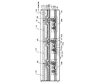
図1はアクティブマトリクス型の発光装置の一部断面を示す図である。 FIG. 1 is a partial cross-sectional view of an active matrix light-emitting device.
第1の基板101上には、3つのTFT103R、103G、103Bを設けている。これらのTFTは、チャネル形成領域120と、ソース領域またはドレイン領域121、122とを活性層とし、ゲート絶縁膜105と、ゲート電極123a、123bを有するpチャネル型TFTである。また、ゲート電極は2層となっており、テーパー形状となっている下層123aと、上層123bとで構成されている。
On the
また、第2の基板116には、R、G、Bの着色層115R、115G、115Bが設けられている。図2(C)に第2の基板に設けられた着色層の配置上面図の一例を示す。なお、R、G、Bの着色層115R、115G、115Bは、それぞれの発光素子に対向して配置されており、TFTに接続されている白色発光素子からの白色光をカラー化している。
The
また、図2(C)にはストライプ状の着色層とした例を示しているが、マトリクス状に着色層を配置してもよい。また、画素の配列をデルタ配列やモザイク配列としてもよい。また、R、G、Bの3種類の画素を用いたフルカラー表示に限らず、3色映像データを4色映像データに変換してR、G、B、W(白色)の4種類の画素を用いたフルカラー表示としてもよい。4種類の画素を用いると、輝度が増加し、躍動感のある映像表示が行える。なお、4種類の画素を用いる場合、Wの画素に対向して着色層は設けない。 FIG. 2C shows an example in which a striped colored layer is used, but the colored layer may be arranged in a matrix. The pixel arrangement may be a delta arrangement or a mosaic arrangement. In addition to full color display using three types of R, G, and B pixels, three-color video data is converted into four-color video data, and four types of R, G, B, and W (white) pixels are converted. The full color display used may be used. When four types of pixels are used, the luminance increases and a lively video display can be performed. Note that when four types of pixels are used, no colored layer is provided to face the W pixels.
また、隔壁109は黒色樹脂であり、異なる着色層との境界(或いは隙間)と重なるブラックマトリクス(BM)の役目を果たしている。従って、隔壁109は、発光領域を囲むように格子形状としている。また、隣り合う着色層において隙間が空いてもよいが、隔壁109の幅よりも隙間の幅が広くならないようにする。
The
図2(D)に第1の基板に設けられた隔壁の上面図の一例を示す。黒い隔壁で囲まれた領域が発光領域と対応して同一面積になっている。また、着色層は発光領域よりも面積を大きくし、視野角を広いものとしている。また、有機化合物層において生じた光の全てが透明電極からTFTの方へ取り出されるわけではなく、例えば、横方向(基板面と平行な方向)にも発光されるが、結果的にこの横方向に発光する光は取り出されないため、ロスになっていた。また、これらの迷光がTFTの活性層に照射されることでTFTの電気特性に影響を与えたり、劣化の原因の一つとなっていた。そこで、本発明は、発光素子からの迷光を黒色樹脂からなる隔壁109で吸収、または遮蔽する構成としている。
FIG. 2D illustrates an example of a top view of a partition provided in the first substrate. The region surrounded by the black partition has the same area corresponding to the light emitting region. The colored layer has a larger area than the light emitting region and a wide viewing angle. In addition, not all of the light generated in the organic compound layer is extracted from the transparent electrode toward the TFT. For example, the light is emitted in the lateral direction (direction parallel to the substrate surface). The light emitted from the light was not taken out, and was lost. In addition, the stray light is applied to the active layer of the TFT, thereby affecting the electrical characteristics of the TFT or causing deterioration. Therefore, in the present invention, stray light from the light emitting element is absorbed or shielded by the
白色発光素子は、第1の電極108a、108bと、有機化合物を含む層110と、透明導電材料からなる第2の電極111とで構成されている。図1では全面に有機化合物を含む層110が設けられているが、白色発光素子であるので1枚のマスクで選択的に形成してもよい。
The white light emitting element includes
また、第1の電極108a、108b及び第2の電極111は仕事関数を考慮して材料を選択する必要がある。但し第1の電極及び第2の電極は、画素構成によりいずれも陽極、又は陰極となりうる。駆動用TFTの極性がpチャネル型である場合、第1の電極を陽極、第2の電極を陰極とするとよい。また、駆動用TFTの極性がNチャネル型である場合、第1の電極を陰極、第2の電極を陽極とすると好ましい。
In addition, it is necessary to select materials for the
ここでは、第1の電極として、金属材料(Ag(銀)、Au(金)、Cu(銅)、W(タングステン)、Al(アルミニウム)など)からなる下層108aと、透明導電材料(インジウム錫酸化物(ITO)、酸化珪素を含むインジウム錫酸化物(ITSO)、酸化亜鉛(ZnO)、酸化スズ(SnO2)など)からなる上層108bとの積層とした例を示している。下層108aとして、反射性を有する層とすれば、発光が第2の基板を通過する上面出射型の発光装置となり、透光性を有する層とすれば、発光が第1の基板および第2の基板を通過する両面出射型の発光装置となる。なお、上面出射型は、下面出射型に比べて、有機化合物を含む層から発光する光が通過する材料層を少なくでき、屈折率の異なる材料層間での迷光を抑えることができる。
Here, as the first electrode, a
中でも好ましい材料は、下層108aとしてAl(C+Ni)合金膜を用い、上層108bとして酸化珪素を含むインジウム錫酸化物(ITSO)を用いる組み合わせである。本実施例では、Al中に0.3atoms%のCと、3atoms%のNiを含有しているAl(C+Ni)合金膜を用いる。なお、Al(C+Ni)合金膜は、通電、或いは熱処理後もITOやITSOとのコンタクト抵抗値に大きな変動がない材料である。また、ITSOは、通電、或いは熱処理によって結晶化しにくく表面の平坦性が高い材料である。
Among them, a preferable material is a combination in which an Al (C + Ni) alloy film is used as the
また、有機化合物を含む層110は、第1の電極(陽極)側から順に、HIL(ホール注入層)、HTL(ホール輸送層)、EML(発光層)、ETL(電子輸送層)、EIL(電子注入層)の順に積層されている。なお、有機化合物を含む層は、積層構造以外に単層構造、又は混合構造をとることができる。 The layer 110 containing an organic compound is formed in order from the first electrode (anode) side: HIL (hole injection layer), HTL (hole transport layer), EML (light emitting layer), ETL (electron transport layer), EIL ( The electron injection layer) is laminated in this order. Note that the layer containing an organic compound can have a single-layer structure or a mixed structure in addition to a stacked structure.
また、水分や脱ガスによるダメージから発光素子を保護するため、第2の電極111を覆う保護膜112を設けることが好ましい。保護膜112としては、PCVD法による緻密な無機絶縁膜(SiN膜、SiNO膜など)、スパッタ法による緻密な無機絶縁膜(SiN膜、SiNO膜など)、炭素を主成分とする薄膜(DLC膜、CN膜、アモルファスカーボン膜)、金属酸化物膜(WO2、CaF2、Al2O3など)などを用いることが好ましい。なお、ダイヤモンドライクカーボン膜(DLC膜とも呼ばれる)は、プラズマCVD法(代表的には、RFプラズマCVD法、マイクロ波CVD法、電子サイクロトロン共鳴(ECR)CVD法、熱フィラメントCVD法など)、燃焼炎法、スパッタ法、イオンビーム蒸着法、レーザー蒸着法などで形成することができる。成膜に用いる反応ガスは、水素ガスと、炭化水素系のガス(例えばCH4、C2H2、C6H6など)とを用い、グロー放電によりイオン化し、負の自己バイアスがかかったカソードにイオンを加速衝突させて成膜する。また、CN膜は反応ガスとしてC2H4ガスとN2ガスとを用いて形成すればよい。なお、DLC膜やCN膜は、膜厚にもよるが、可視光に対して透明もしくは半透明な絶縁膜である。可視光に対して透明とは可視光の透過率が80〜100%であることを指し、可視光に対して半透明とは可視光の透過率が50〜80%であることを指す。
In addition, in order to protect the light-emitting element from damage due to moisture or degassing, it is preferable to provide a
また、保護膜112上には、光触媒機能を有する物質を含む下地層(バッファー層とも言う)113が設けられている。光触媒機能を有する物質としては、スパッタ法またはスプレー法により得られる酸化チタン(TiOX)、チタン酸ストロンチウム(SrTiO3)、セレン化カドミウム(CdSe)、タンタル酸カリウム(KTaO3)、硫化カドミウム(CdS)、酸化ジルコニウム(ZrO2)、酸化ニオブ(Nb2O5)、酸化亜鉛(ZnO)、酸化鉄(Fe2O3)、酸化タングステン(WO3)が挙げられる。下地層113は透光性を持たせることが好ましい。なお、この下地層113は、保護膜としても機能する。
Further, an underlayer (also referred to as a buffer layer) 113 including a substance having a photocatalytic function is provided over the
第1の基板101と第2の基板116との間は、充填材料114が充填されている。第1の基板と第2の基板とを貼り合わせるシール材と充填材料114との密着性や、保護膜と充填材料114との密着性を向上させるために光触媒機能を有する物質を含む下地層113が設けられている。なお、貼り合わせる前に、予め光触媒活性化させる波長の光を下地層113に照射しておく。また、第2の基板116側にも着色層を覆うオーバーコート層として光触媒機能を有する物質を含む層を設けてもよい。
A filling material 114 is filled between the
また、ここでは第2の基板116の第1の基板101に近い面に着色層を設けた例を示しているが、第2の基板116の外側面に着色層を設けてもよく、その場合には第2の基板116と充填材料114とが接する構造となる。
Although an example in which a colored layer is provided on the surface of the
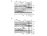
図2(A)、図2(B)は貼り合わせる前のそれぞれの基板の様子を斜視図で示したものである。図2(A)、図2(B)では1つの基板で4枚のパネルを作製する多面取りを行っている。図2(A)に示す第1の基板201には、BM209および白色発光素子が配置されている画素部202を設けており、画素部202を覆うように光触媒物質形成領域203を設けている。なお、図2(D)にBM209の一部を示す。図2(B)に示す第2の基板216には、画素部と重なる着色層204を囲むようにシール205が設けられ、シール205で囲まれた領域に充填材料206が液滴吐出法により滴下されている。なお、図2(C)に着色層204の一部を示す。
2A and 2B are perspective views showing the state of the respective substrates before bonding. In FIG. 2A and FIG. 2B, multi-chamfering is performed in which four panels are manufactured using one substrate. A
そして、貼り合わせ装置で光触媒物質形成領域203と充填材料206、およびシール205と接するようにし、気泡が入らないように第1の基板と第2の基板とを貼り合わせる。 Then, the first substrate and the second substrate are bonded together so that the photocatalyst substance forming region 203, the filling material 206, and the seal 205 are brought into contact with each other by a bonding apparatus, and air bubbles do not enter.
図3に貼り合わせ装置の一例を示す。図3に示す貼り合わせ装置は、減圧雰囲気で貼り合わせることが可能な装置である。 FIG. 3 shows an example of a bonding apparatus. The bonding apparatus illustrated in FIG. 3 is an apparatus capable of bonding in a reduced pressure atmosphere.
図3中、40は第1基板支持台、41bは真空チャンバー上部、41aは真空チャンバー下部、42は第2基板支持台、48は下側定盤である。図3(A)は貼り合わせ前の状態を示している。 In FIG. 3, 40 is a first substrate support, 41b is an upper part of a vacuum chamber, 41a is a lower part of the vacuum chamber, 42 is a second substrate support, and 48 is a lower surface plate. FIG. 3A shows a state before bonding.
貼り合わせ時には、真空チャンバー上部41bを真空チャンバー下部41aと接するように下降させた後、排気してチャンバー内を減圧とする。そして、第1基板支持台40に対向している第2基板支持台42を下降させた後、圧力をかけて第1基板35と第2基板31を貼り合わせ、そのまま加熱することによって硬化させる。第2基板支持台42および下側定盤48は加熱ヒータが内蔵されており、シール材32および充填材料33を硬化させる。貼り合わせ後の状態を図3(B)に示す。さらにシール材の描画も減圧下で行ってもよい。 At the time of bonding, the vacuum chamber upper portion 41b is lowered so as to be in contact with the vacuum chamber lower portion 41a and then evacuated to reduce the pressure in the chamber. Then, after the second substrate support 42 facing the first substrate support 40 is lowered, the first substrate 35 and the second substrate 31 are bonded together by applying pressure and cured by heating as it is. The second substrate support 42 and the lower surface plate 48 have a built-in heater, and cure the sealing material 32 and the filling material 33. The state after bonding is shown in FIG. Furthermore, the sealing material may be drawn under reduced pressure.
また、液滴吐出装置の例を図4に示す。図4において、300は第2の基板、304は撮像手段、307はステージ、311はマーカー、303は1つの画素部を囲むシールを示している。1つの画素部の幅と同じ幅のヘッド305a、305bを備え、ステージを移動させてこれらのヘッドを走査、例えばジグザグまたは往復させて適宜、充填材料を滴下する。基板の幅と同じ幅のヘッドとすることも可能であるが、図4のように1つのパネルサイズに合わせるほうが操作しやすい。また、スループット向上のためには、ステージを動かしたままで充填材料の吐出を行うことが好ましい。
An example of a droplet discharge device is shown in FIG. In FIG. 4,
貼り合わせた後は、所望のサイズに基板を分断すればよい。 After bonding, the substrate may be divided into a desired size.
第1の基板101上に形成する下地絶縁膜102としては、PCVD法による無機絶縁膜(SiN膜、SiNO膜など)の単層または積層を用いる。また、PCVD法による無機絶縁膜(SiN膜、SiNO膜など)を用いて層間絶縁膜106を形成している。
As the
また、層間絶縁膜106上に設けられる高耐熱性平坦化膜107は、塗布法による平坦な層間絶縁膜である。塗布法による平坦な層間絶縁膜とは、液状の組成物を塗布して形成する層間絶縁膜を指す。塗布法による平坦な層間絶縁膜としては、アクリル、ポリイミドなどの有機樹脂、有機溶媒中に溶かされた絶縁膜材料を塗布した後熱処理により被膜を形成する所謂、塗布珪素酸化膜(Spin on Glass、以下「SOG」ともいう。)、シロキサンポリマーなどの焼成によりシロキサン結合(Si−O−Si結合)を形成する材料膜などが挙げられる。また、高耐熱性平坦化膜107は、塗布法に限定されず、気相成長法やスパッタリング法により形成された酸化珪素膜などの無機絶縁膜も用いることができる。また、保護膜として窒化珪素膜をPCVD法やスパッタ法で形成した後、塗布法による平坦な絶縁膜を積層してもよい。
Further, the high heat-
また、白色発光素子においては、第1の電極が平坦とすることが重要であり、高耐熱性平坦化膜107が平坦でない場合、高耐熱性平坦化膜107の表面凹凸の影響によって第1の電極も平坦とならない恐れがある。従って、高耐熱性平坦化膜107の平坦性は重要である。
In the white light emitting element, it is important that the first electrode is flat. When the high heat
また、TFTのドレイン配線、またはソース配線124a、124b、124cは、3層構造としている。ここでは、Ti膜と、Al(C+Ni)合金膜と、Ti膜との積層膜を用いる。TFTのドレイン配線、またはソース配線は、層間絶縁膜のカバレッジを考慮して、テーパー形状とすることが好ましい。
The drain wiring or
また、ここではトップゲート型TFTを例として説明したが、TFT構造に関係なく本発明を適用することが可能であり、例えばボトムゲート型(逆スタガ型)TFTや順スタガ型TFTに適用することが可能である。 Although the top gate type TFT has been described as an example here, the present invention can be applied regardless of the TFT structure. For example, it can be applied to a bottom gate type (reverse stagger type) TFT or a forward stagger type TFT. Is possible.
以上の構成でなる本発明について、以下に示す実施例でもってさらに詳細な説明を行うこととする。 The present invention having the above-described configuration will be described in more detail with the following examples.
本実施例では図5(A)を用いて、上面出射型の発光装置の作製例を示す。 In this embodiment, an example of manufacturing a top emission light-emitting device will be described with reference to FIG.
まず、第1の基板401上に下地絶縁膜を形成する。第1の基板401は平坦性および耐熱性を有している基板であれば特に限定されない。下地絶縁膜としては、酸化シリコン膜、窒化シリコン膜または酸化窒化シリコン膜などの絶縁膜から成る下地膜を形成する。
First, a base insulating film is formed over the
次いで、下地絶縁膜上に半導体層を形成する。半導体層は、非晶質構造を有する半導体膜を公知の手段(スパッタ法、LPCVD法、またはプラズマCVD法等)により成膜した後、公知の結晶化処理(レーザー結晶化法、熱結晶化法、またはニッケルなどの触媒を用いた熱結晶化法等)を行って得られた結晶質半導体膜を第1のフォトマスクを用いて所望の形状にパターニングして形成する。この半導体層の厚さは25〜80nm(好ましくは30〜70nm)の厚さで形成する。結晶質半導体膜の材料に限定はないが、好ましくはシリコンまたはシリコンゲルマニウム(SiGe)合金などで形成すると良い。 Next, a semiconductor layer is formed over the base insulating film. The semiconductor layer is formed by forming a semiconductor film having an amorphous structure by a known means (sputtering method, LPCVD method, plasma CVD method, etc.), and then known crystallization treatment (laser crystallization method, thermal crystallization method). Or a crystalline semiconductor film obtained by performing a thermal crystallization method using a catalyst such as nickel) is formed by patterning into a desired shape using a first photomask. The semiconductor layer is formed with a thickness of 25 to 80 nm (preferably 30 to 70 nm). There is no limitation on the material of the crystalline semiconductor film, but the crystalline semiconductor film is preferably formed of silicon or a silicon germanium (SiGe) alloy.
また、非晶質構造を有する半導体膜の結晶化処理として連続発振のレーザーを用いてもよく、非晶質半導体膜の結晶化に際し、大粒径の結晶を得るためには、連続発振が可能な固体レーザを用い、基本波の第2高調波〜第4高調波を適用するのが好ましい。代表的には、Nd:YVO4レーザー(基本波1064nm)の第2高調波(532nm)や第3高調波(355nm)を適用すればよい。連続発振のレーザーを用いる場合には、出力10Wの連続発振のYVO4レーザから射出されたレーザ光を非線形光学素子により高調波に変換する。また、共振器の中にYVO4結晶と非線形光学素子を入れて、高調波を射出する方法もある。そして、好ましくは光学系により照射面にて矩形状または楕円形状のレーザ光に成形して、被処理体に照射する。このときのエネルギー密度は0.01〜100MW/cm2程度(好ましくは0.1〜10MW/cm2)が必要である。そして、10〜2000cm/s程度の速度でレーザ光に対して相対的に半導体膜を移動させて照射すればよい。 In addition, a continuous wave laser may be used as a crystallization process for a semiconductor film having an amorphous structure, and in order to obtain a crystal having a large grain size when crystallizing an amorphous semiconductor film, continuous wave is possible. It is preferable to use a solid-state laser and apply the second to fourth harmonics of the fundamental wave. Typically, a second harmonic (532 nm) or a third harmonic (355 nm) of an Nd: YVO 4 laser (fundamental wave 1064 nm) may be applied. In the case of using a continuous wave laser, laser light emitted from a continuous wave YVO 4 laser having an output of 10 W is converted into a harmonic by a non-linear optical element. There is also a method of emitting harmonics by putting a YVO 4 crystal and a nonlinear optical element in a resonator. Then, it is preferably formed into a rectangular or elliptical laser beam on the irradiation surface by an optical system, and irradiated to the object to be processed. At this time, the energy density of approximately 0.01 to 100 MW / cm 2 (preferably 0.1 to 10 MW / cm 2) is required. Then, irradiation may be performed by moving the semiconductor film relative to the laser light at a speed of about 10 to 2000 cm / s.
次いで、レジストマスクを除去した後、半導体層を覆うゲート絶縁膜を形成する。ゲート絶縁膜はプラズマCVD法またはスパッタ法または熱酸化法を用い、厚さを1〜200nmとする。 Next, after removing the resist mask, a gate insulating film is formed to cover the semiconductor layer. The gate insulating film is formed by plasma CVD, sputtering, or thermal oxidation, and has a thickness of 1 to 200 nm.
次いで、ゲート絶縁膜上に膜厚100〜600nmの導電膜を形成する。ここでは、スパッタ法を用い、TaN膜とW膜との積層からなる導電膜を形成する。なお、ここでは導電膜をTaN膜とW膜との積層としたが、特に限定されず、Ta、W、Ti、Mo、Al、Cuから選ばれた元素、または前記元素を主成分とする合金材料若しくは化合物材料の単層、またはこれらの積層で形成してもよい。また、リン等の不純物元素をドーピングした多結晶シリコン膜に代表される半導体膜を用いてもよい。 Next, a conductive film with a thickness of 100 to 600 nm is formed over the gate insulating film. Here, a conductive film formed by stacking a TaN film and a W film is formed by sputtering. Here, the conductive film is a laminate of a TaN film and a W film, but is not particularly limited, and an element selected from Ta, W, Ti, Mo, Al, and Cu, or an alloy containing the above element as a main component A single layer of a material or a compound material, or a stacked layer thereof may be used. Alternatively, a semiconductor film typified by a polycrystalline silicon film doped with an impurity element such as phosphorus may be used.
次いで、第2のフォトマスクを用いてレジストマスクを形成し、ドライエッチング法またはウェットエッチング法を用いてエッチングを行う。このエッチング工程によって、導電膜をエッチングして、TFT404のゲート電極を形成する。
Next, a resist mask is formed using a second photomask, and etching is performed using a dry etching method or a wet etching method. Through this etching process, the conductive film is etched to form the gate electrode of the
次いで、レジストマスクを除去した後、第3のフォトマスクを用いてレジストマスクを新たに形成し、ここでは図示しないnチャネル型TFTを形成するため、半導体にn型を付与する不純物元素(代表的にはリン、またはAs)を低濃度にドープするための第1のドーピング工程を行う。レジストマスクは、pチャネル型TFTとなる領域と、導電層の近傍とを覆う。この第1のドーピング工程によって絶縁膜を介してスルードープを行い、n型の低濃度不純物領域を形成する。一つの発光素子は、複数のTFTを用いて駆動させるが、pチャネル型TFTのみで駆動させる場合には、上記ドーピング工程は特に必要ない。 Next, after removing the resist mask, a resist mask is newly formed using a third photomask. In order to form an n-channel TFT (not shown) here, an impurity element imparting n-type conductivity (typical) First, a first doping step is performed for doping phosphorus or As) at a low concentration. The resist mask covers a region to be a p-channel TFT and the vicinity of the conductive layer. Through-doping is performed through the insulating film in the first doping step, and an n-type low concentration impurity region is formed. One light emitting element is driven by using a plurality of TFTs, but the above doping step is not particularly necessary when driven by only a p-channel TFT.
次いで、レジストマスクを除去した後、第4のフォトマスクを用いてレジストマスクを新たに形成し、半導体にp型を付与する不純物元素(代表的にはボロン)を高濃度にドープするための第2のドーピング工程を行う。この第2のドーピング工程によってゲート絶縁膜を介してスルードープを行い、p型の高濃度不純物領域を形成する。 Next, after removing the resist mask, a resist mask is newly formed by using a fourth photomask, and a semiconductor film is doped with an impurity element (typically boron) imparting p-type conductivity to the semiconductor at a high concentration. Step 2 is performed. Through-doping is performed through the gate insulating film in the second doping step, and a p-type high concentration impurity region is formed.
次いで、第5のフォトマスクを用いてレジストマスクを新たに形成し、ここでは図示しないnチャネル型TFTを形成するため、半導体にn型を付与する不純物元素(代表的にはリン、またはAs)を高濃度にドープするための第3のドーピング工程を行う。レジストマスクは、pチャネル型TFTとなる領域と、導電層の近傍とを覆う。この第3のドーピング工程によってゲート絶縁膜を介してスルードープを行い、n型の高濃度不純物領域を形成する。 Next, a resist mask is newly formed using a fifth photomask, and an impurity element imparting n-type conductivity to the semiconductor (typically phosphorus or As) is formed in order to form an n-channel TFT (not shown) here. A third doping step is performed to dope the silicon at a high concentration. The resist mask covers a region to be a p-channel TFT and the vicinity of the conductive layer. Through-doping is performed through the gate insulating film in the third doping step to form an n-type high concentration impurity region.
この後、レジストマスクを除去し、水素を含む絶縁膜を成膜した後、半導体層に添加された不純物元素の活性化および水素化を行う。水素を含む絶縁膜は、PCVD法により得られる窒化酸化珪素膜(SiNO膜)を用いる。 After that, after removing the resist mask and forming an insulating film containing hydrogen, the impurity element added to the semiconductor layer is activated and hydrogenated. As the insulating film containing hydrogen, a silicon nitride oxide film (SiNO film) obtained by a PCVD method is used.
次いで、層間絶縁膜の2層目となる平坦化膜410を形成する。平坦化膜410としては、無機材料(酸化シリコン、窒化シリコン、酸化窒化シリコンなど)、感光性または非感光性の有機材料(ポリイミド、アクリル、ポリアミド、ポリイミドアミド、レジストまたはベンゾシクロブテン)、またはこれらの積層などを用いる。また、平坦化膜に用いる他の膜としては、塗布法によって得られるアルキル基を含むSiOx膜からなる絶縁膜、例えばシリカガラス、アルキルシロキサンポリマー、アルキルシルセスキオキサンポリマー、水素化シルセスキオキサンポリマー、水素化アルキルシルセスキオキサンポリマーなどを用いて形成された絶縁膜を用いることができる。シロキサン系ポリマーの一例としては、東レ製塗布絶縁膜材料であるPSB−K1、PSB−K31や触媒化成製塗布絶縁膜材料であるZRS−5PHが挙げられる。
Next, a
次いで、第6のマスクを用いて層間絶縁膜にコンタクトホールを形成する。次いで、第6のマスクを除去し、導電膜(TiN膜、Al(C+Ni)合金膜、TiN膜を順次積層した導電膜)を形成した後、第7のマスクを用いてエッチングを行い、配線(TFTのソース配線及びドレイン配線や、電流供給配線など)を形成する。 Next, contact holes are formed in the interlayer insulating film using a sixth mask. Next, after removing the sixth mask and forming a conductive film (a conductive film in which a TiN film, an Al (C + Ni) alloy film, and a TiN film are sequentially stacked), etching is performed using the seventh mask, and wiring ( TFT source wiring and drain wiring, current supply wiring, etc.) are formed.
次いで、第7のマスクを除去し、3層目の層間絶縁膜411を形成する。3層目の層間絶縁膜411としては、塗布法によって得られる黒色顔料を分散させてなる感光性または非感光性の有機材料を用いる。本実施例では、コントラスト向上、迷光の吸収のために遮光性を有する層間絶縁膜を用いている。さらに3層目の層間絶縁膜を保護するため、4層目の層間絶縁膜としてPCVD法により得られる窒化酸化珪素膜(SiNO膜)を積層してもよい。4層目の層間絶縁膜を設けた場合、後の工程で第1の電極をパターニングした後、第1の電極をマスクとして選択的に除去することが好ましい。
Next, the seventh mask is removed, and a third
次いで、第8のマスクを用いて層間絶縁膜にコンタクトホールを形成する。 Next, contact holes are formed in the interlayer insulating film using an eighth mask.
次いで、反射導電膜と透明導電膜を成膜した後、第9のマスクを用いてパターニングを行って反射電極412と透明電極413との積層を得る。反射電極412としては、Ag、Al、またはAl(C+Ni)合金膜を用いる。透明電極413としては、インジウム錫酸化物(ITO)の他、例えば、Si元素を含むインジウム錫酸化物(ITSO)や酸化インジウムに2〜20%の酸化亜鉛(ZnO)を混合したIZO(Indium Zinc Oxide)などの透明導電材料を用いることができる。
Next, after forming a reflective conductive film and a transparent conductive film, patterning is performed using a ninth mask to obtain a stack of the
次いで、第10のマスクを用いて反射電極412及び透明電極413の端部を覆って隔壁、即ち、ブラックマトリクス(BM)となる、遮光性を有する絶縁物419を形成する。遮光性を有する絶縁物としては、黒色顔料を分散させてなる感光性または非感光性の有機材料(ポリイミド、アクリル、ポリアミド、ポリイミドアミド、レジストまたはベンゾシクロブテン)、またはSOG膜(例えば、アルキル基を含むSiOx膜)を膜厚0.8μm〜1μmの範囲で用いる。例えば、富士フィルムオーリン社製COLOR MOSAIC CK(商品名)のような材料を用いる。なお、本実施例では、層間絶縁膜411も遮光性を有する絶縁物で設けることによって、層間絶縁膜411とのトータルで遮光の効果を得ることができ、絶縁物419の厚さを薄くしたり、遮光性の低い材料を用いることもできる。
Next, an insulating
次いで、有機化合物を含む層414を、蒸着法または塗布法を用いて形成する。白色発光を得るためには、様々な方法があるが、本実施例では塗布により形成可能な高分子材料からなる発光層を用いる場合について説明する。この場合、発光層となる高分子材料への色素ドーピングは溶液調整で行うことができ、複数の色素をドーピングする共蒸着を行う蒸着法に比べて極めて容易に得ることができる。具体的には、陽極上に、正孔注入層として作用するポリ(エチレンジオキシチオフェン)/ポリ(スチレンスルホン酸)水溶液(PEDOT/PSS)を全面に塗布、焼成した後、発光層として作用する発光中心色素(1,1,4,4−テトラフェニル−1,3−ブタジエン(TPB)、4−ジシアノメチレン−2−メチル−6−(p−ジメチルアミノ−スチリル)−4H−ピラン(DCM1)、ナイルレッド、クマリン6など)をドープしたポリビニルカルバゾール(PVK)溶液を全面に塗布、焼成する。なお、PEDOT/PSSは溶媒に水を用いており、有機溶剤には溶けない。従って、PVKをその上から塗布する場合にも、再溶解する心配はない。また、PEDOT/PSSとPVKは溶媒が異なるため、成膜室は同一のものを使用しないことが好ましい。
Next, a
また、本実施例では高分子材料からなる有機化合物膜を積層とした例を示したが、有機化合物層を単層とすることもできる。例えば、ホール輸送性を有するポリビニルカルバゾール(PVK)に電子輸送性を有する1,3,4−オキサジアゾール誘導体(PBD)を分散させてもよい。また、30wt%のPBDを電子輸送剤として分散し、4種類の色素(TPB、クマリン6、DCM1、ナイルレッド)を適当量分散することで白色発光が得られる。また、赤色発光する有機化合物膜や緑色発光する有機化合物膜や青色発光する有機化合物膜を適宜選択し、重ねて混色させることによって全体として白色発光を得ることも可能である。 In this embodiment, an example in which an organic compound film made of a polymer material is stacked is shown, but the organic compound layer may be a single layer. For example, a 1,3,4-oxadiazole derivative (PBD) having an electron transport property may be dispersed in polyvinyl carbazole (PVK) having a hole transport property. Further, white light emission can be obtained by dispersing 30 wt% PBD as an electron transporting agent and dispersing an appropriate amount of four kinds of dyes (TPB, coumarin 6, DCM1, Nile red). It is also possible to obtain white light emission as a whole by appropriately selecting an organic compound film emitting red light, an organic compound film emitting green light, or an organic compound film emitting blue light and mixing them in layers.
なお、発光素子の信頼性を向上させるため、有機化合物を含む層414の形成前に真空加熱を行って脱気を行うことが好ましい。例えば、有機化合物材料の蒸着を行う前に、基板に含まれるガスを除去するために減圧雰囲気や不活性雰囲気で200℃〜300℃の加熱処理を行うことが望ましい。
Note that in order to improve the reliability of the light-emitting element, it is preferable to perform deaeration by performing vacuum heating before the formation of the
次いで、有機化合物を含む層414の上に透明電極415、即ち、有機発光素子の陰極を膜厚10nm〜800nmの範囲で形成する。透明電極415としては、インジウム錫酸化物(ITO)の他、例えば、Si元素を含むインジウム錫酸化物(ITSO)や酸化インジウムに2〜20%の酸化亜鉛(ZnO)を混合したIZOを用いることができる。
Next, the
以上のようにして、白色発光素子が作製される。白色発光素子を構成する陽極、有機化合物を含む層および陰極の各材料は適宜選択し、各膜厚も調整する。陽極と陰極とで同じ材料を用い、且つ、同程度の膜厚、好ましくは100nm程度の薄い膜厚とすることが望ましい。 As described above, a white light emitting element is manufactured. The materials for the anode, the layer containing the organic compound, and the cathode constituting the white light-emitting element are appropriately selected, and the film thicknesses are also adjusted. It is desirable that the same material is used for the anode and the cathode, and the film thickness is approximately the same, preferably approximately 100 nm.
次いで、発光素子を覆って、水分の侵入を防ぐ透明保護層416を形成する。透明保護層416としては、スパッタ法またはCVD法により得られる窒化珪素膜、酸化珪素膜、酸化窒化珪素膜(SiNO膜(組成比N>O)またはSiON膜(組成比N<O))、炭素を主成分とする薄膜(例えばDLC膜、CN膜)などを用いることができる。
Next, a transparent
次いで、ぬれ性を向上させるために光触媒物質を含む下地層405を形成する。光触媒物質としてスパッタリング法により所定の結晶構造を有するTiO2結晶を形成する。ターゲットには金属チタンチューブを用い、アルゴンガスと酸素を用いてスパッタリングを行う。更にHeガスを導入してもよい。光触媒活性の高いTiO2を形成するためには、酸素を多く含む雰囲気とし、形成圧力を高めにする。更に成膜室又は処理物が設けられた基板を加熱しながらTiO2を形成すると好ましい。このように形成されるTiO2は非常に薄膜(1μm 程度)であっても光触媒機能を有する。その後、選択的に光照射を行って照射領域を形成するため、光学系を用いて光を集光させる。そして照射領域におけるTiO2は、親水性を示す。なお光照射時間により、親水性と親油性を共に有する状態にもなりうる。
Next, a
次いで、基板間隔を確保するためのギャップ材(フィラー(ファイバーロッド)、微粒子(真絲球など)など)を含有するシール材を用い、着色層402G、402Rが設けられた第2の基板403と基板401とを貼り合わせる。なお、一対の基板間には充填材料417、代表的には紫外線硬化または熱硬化のエポキシ樹脂を充填する。また、第2の基板403は、光透過性を有するガラス基板や石英基板やプラスチック基板を用いればよい。透明な充填材料(屈折率1.50程度)を一対の基板間に充填することによって、一対の基板間を空間(不活性気体)とした場合に比べて全体の透過率を向上させることができる。
Next, a
本実施例の発光素子は、透明電極415、透明保護層416、光触媒物質を含む下地層405、および充填材料417が透光性材料で形成され、図5(A)の白抜きの矢印で表すように、上面側から採光することができる。
In the light-emitting element of this example, a
また、本実施例は実施の形態と自由に組み合わせることができる。 This embodiment can be freely combined with the embodiment mode.
本実施例では、図5(B)を用いて、両面出射型の発光装置の作製例を示す。 In this embodiment, an example of manufacturing a dual emission light-emitting device will be described with reference to FIG.
まず、透光性を有する第1の基板501上に下地絶縁膜を形成する。第1の基板501は透光性を有する基板であれば特に限定されない。下地絶縁膜としては、酸化シリコン膜、窒化シリコン膜または酸化窒化シリコン膜などの絶縁膜から成る下地膜を形成する。
First, a base insulating film is formed over a light-transmitting
次いで、実施例1と同様にして下地絶縁膜上に半導体層を形成する。次いで、実施例1と同様にして半導体層を覆うゲート絶縁膜、ゲート絶縁膜上にゲート電極を形成する。 Next, in the same manner as in Example 1, a semiconductor layer is formed over the base insulating film. Next, in the same manner as in Example 1, a gate insulating film covering the semiconductor layer and a gate electrode are formed on the gate insulating film.
次いで、実施例1と同様にして適宜、ドーピングを行ってn型の低濃度不純物領域、p型の高濃度不純物領域、n型の高濃度不純物領域などを形成する。次いで、レジストマスクを除去し、水素を含む絶縁膜(透光性を有する層間絶縁膜)を成膜した後、半導体層に添加された不純物元素の活性化および水素化を行う。 Next, as in Example 1, doping is appropriately performed to form an n-type low concentration impurity region, a p-type high concentration impurity region, an n-type high concentration impurity region, and the like. Next, after removing the resist mask and forming an insulating film containing hydrogen (a light-transmitting interlayer insulating film), the impurity element added to the semiconductor layer is activated and hydrogenated.
次いで、層間絶縁膜の2層目となる透光性を有する平坦化膜510を形成する。透光性を有する平坦化膜510としては、無機材料(酸化シリコン、窒化シリコン、酸化窒化シリコンなど)、感光性または非感光性の有機材料(ポリイミド、アクリル、ポリアミド、ポリイミドアミド、レジストまたはベンゾシクロブテン)、またはこれらの積層などを用いる。
Next, a light-transmitting
次いで、実施例1と同様に層間絶縁膜にコンタクトホールを形成した後、導電膜(TiN膜、Al(C+Ni)合金膜、TiN膜を順次積層)を形成した後、エッチングを選択的に行い、配線(TFT504のソース配線及びドレイン配線や、電流供給配線など)を形成する。
Next, after forming a contact hole in the interlayer insulating film in the same manner as in Example 1, a conductive film (TiN film, Al (C + Ni) alloy film, TiN film is sequentially laminated) is formed, and etching is selectively performed. Wiring (source wiring and drain wiring of
次いで、3層目の層間絶縁膜511を形成する。3層目の層間絶縁膜511としては、塗布法によって得られるアルキル基を含むSiOx膜からなる絶縁膜を用いる。さらに3層目の層間絶縁膜を保護するため、4層目の層間絶縁膜としてPCVD法により得られる窒化酸化珪素膜(SiNO膜)を積層してもよい。4層目の層間絶縁膜を設けた場合、後の工程で第1の電極をパターニングした後、第1の電極をマスクとして選択的に除去することが好ましい。
Next, a third
次いで、層間絶縁膜にコンタクトホールを形成する。 Next, contact holes are formed in the interlayer insulating film.
次いで、透明導電膜を成膜した後、パターニングを行って透明電極513を得る。透明電極513としては、インジウム錫酸化物(ITO)の他、例えば、Si元素を含むインジウム錫酸化物(ITSO)や酸化インジウムに2〜20%の酸化亜鉛(ZnO)を混合したIZOなどの仕事関数の高い(仕事関数4.0eV以上)透明導電材料を用いる。
Next, after forming a transparent conductive film, patterning is performed to obtain a
次いで、マスクを用いて透明電極513の端部を覆ってブラックマトリクス(BM)となる、遮光性を有する絶縁物519を形成する。遮光性を有する絶縁物としては、黒色顔料を分散させてなる感光性または非感光性の有機材料(ポリイミド、アクリル、ポリアミド、ポリイミドアミド、レジストまたはベンゾシクロブテン)、またはSOG膜(例えば、アルキル基を含むSiOx膜)を膜厚0.8μm〜1μmの範囲で用いる。
Next, an insulating
次いで、実施例1と同様にして有機化合物を含む層514を、蒸着法または塗布法を用いて形成する。
Next, a
次いで、有機化合物を含む層514の上に透明電極515、即ち、有機発光素子の陰極を膜厚10nm〜800nmの範囲で形成する。透明電極515としては、インジウム錫酸化物(ITO)の他、例えば、Si元素を含むインジウム錫酸化物(ITSO)や酸化インジウムに2〜20%の酸化亜鉛(ZnO)を混合したIZOを用いることができる。
Next, the
以上のようにして、白色発光素子が作製される。 As described above, a white light emitting element is manufactured.
次いで、実施例1と同様に、発光素子を覆って、水分の侵入を防ぐ透明保護層516を形成する。透明保護層516としては、スパッタ法またはCVD法により得られる窒化珪素膜、酸化珪素膜、酸化窒化珪素膜(SiNO膜(組成比N>O)またはSiON膜(組成比N<O))、炭素を主成分とする薄膜(例えばDLC膜、CN膜)などを用いることができる。
Next, as in Example 1, a transparent
次いで、実施例1と同様に、ぬれ性を向上させるために光触媒物質を含む下地層505を形成する。
Next, as in Example 1, a
次いで、基板間隔を確保するためのギャップ材(フィラー(ファイバーロッド)、微粒子(真絲球など)など)を含有するシール材を用い、着色層502G、502Rが設けられた第2の基板503と基板501とを貼り合わせる。なお、一対の基板間には充填材料517、代表的には紫外線硬化または熱硬化のエポキシ樹脂を充填する。また、第2の基板503は、光透過性を有するガラス基板や石英基板やプラスチック基板を用いればよい。
Next, a
本実施例の発光素子は、透明電極515、充填材料517が透光性材料で形成され、図5(B)の白抜きの矢印で表すように、上面側および下面側の両方から採光することができる。
In the light-emitting element of this example, the
最後に光学フィルム(偏光板、または円偏光板)506、507を設けてコントラストを向上させる。 Finally, optical films (polarizing plate or circularly polarizing plate) 506 and 507 are provided to improve contrast.
例えば、基板501に光学フィルム(基板に近い順に、λ/4板と、偏光板とを配置)507を設け、第2の基板503に光学フィルム(基板に近い順に、λ/4板と、偏光板とを配置)506を設ける。
For example, an optical film (a λ / 4 plate and a polarizing plate are arranged in the order close to the substrate) 507 is provided on the
また、他の例として、基板501に光学フィルム(基板に近い順に、λ/4板と、λ/2板と、偏光板とを配置)507を設け、第2の基板503に光学フィルム(基板に近い順に、λ/4板と、λ/2板と、偏光板とを配置)506を設ける。
As another example, an optical film (a λ / 4 plate, a λ / 2 plate, and a polarizing plate are arranged in the order close to the substrate) 507 is provided on the
このように、本発明は両面出射型表示装置の構成に応じて、偏光板、円偏光板、またはそれらを組み合わせて設けることができる。その結果、きれいな黒表示を行え、コントラストが向上する。さらに、円偏光板を設けることにより反射光を防止することができる。 As described above, the present invention can be provided with a polarizing plate, a circularly polarizing plate, or a combination thereof depending on the structure of the dual emission display device. As a result, a clear black display can be performed and the contrast is improved. Furthermore, reflection light can be prevented by providing a circularly polarizing plate.
また、本実施例は実施の形態、または実施例1と自由に組み合わせることができる。 Further, this embodiment can be freely combined with the embodiment mode or Embodiment 1.
本実施例では、図6を用いてボトムゲート型(逆スタガ型とも呼ぶ)のTFTを用いた発光装置の作製例を示す。 In this embodiment, an example of manufacturing a light-emitting device using a bottom-gate (also referred to as an inverted staggered) TFT will be described with reference to FIGS.
まず、基板601上に下地絶縁膜602を形成する。下地絶縁膜602として酸化シリコン膜、窒化シリコン膜または酸化窒化シリコン膜(SiOxNy)等の絶縁膜を用いることが好ましい。なお、基板601は、無アルカリガラス基板の他、本作製工程の処理温度に耐えうる耐熱性を有するプラスチック基板等を用いることができる。
First, the
次いで、下地絶縁膜602上に膜厚100〜600nmの導電膜を形成する。導電膜としては、タンタル(Ta)、チタン(Ti)、モリブデン(Mo)、タングステン(W)、クロム(Cr)、シリコン(Si)、スカンジウム(Sc)、Nd、Al、Cuから選ばれた元素、または前記元素を組み合わせた合金膜(代表的には、Mo―W合金、Mo―Ta合金)を用いることができる。
Next, a conductive film with a thickness of 100 to 600 nm is formed over the
次いで、フォトマスクを用いてレジストマスクを形成し、ドライエッチング法またはウェットエッチング法を用いてエッチングを行う。このエッチング工程によって、導電膜をエッチングして、導電層623を得る。なお、導電層623はTFT603R、603G、603Bのゲート電極となる。後の工程で薄い半導体膜を形成するため、カバレッジ不良が生じないように導電層の端面形状はテーパー形状となるようにエッチングすることが好ましい。
Next, a resist mask is formed using a photomask, and etching is performed using a dry etching method or a wet etching method. Through this etching step, the conductive film is etched to obtain the
次いで、レジストマスクを除去した後、導電層を覆う絶縁膜605を形成する。絶縁膜605はプラズマCVD法またはスパッタ法を用いて得られる酸化シリコン膜、窒化シリコン膜または酸化窒化シリコン膜(SiOxNy)等の絶縁膜単層または積層膜を用い、厚さを50〜200nmとする。例えば、下層を窒化シリコン膜とし、上層を酸化シリコン膜とする積層構造としても良い。なお、絶縁膜605はTFTのゲート絶縁膜となる。勿論、ゲート絶縁膜は上記材料に限定されず、酸化タンタル膜などの他の絶縁膜を用いても良い。ただし、絶縁膜605の成膜温度で導電層623がダメージを受けないようにする。
Next, after removing the resist mask, an insulating
次いで、絶縁膜605上に50〜200nm(好ましくは100〜150nm)の厚さで非晶質構造を含む半導体膜、或いは結晶構造を含む半導体膜を、プラズマCVD法を用いて全面に形成する。本実施例では、SiH4ガスとF2ガスを原料ガスに用いてセミアモルファスシリコン膜を成膜する。また、SiH4とF2の混合気体を用いたPCVD法により得られるセミアモルファスシリコン膜にレーザー光を照射して、さらに結晶性を向上させてもよい。
Next, a semiconductor film including an amorphous structure or a crystal structure having a thickness of 50 to 200 nm (preferably 100 to 150 nm) is formed over the entire surface of the insulating
他のセミアモルファス半導体膜の成膜方法としては、SiH4をH2で3倍〜1000倍に希釈した混合気体、Si2H6とGeF4のガス流量比を20〜40:0.9(Si2H6:GeF4)で希釈した混合気体、或いはSi2H6とF2の混合気体、或いはSiH4とSiF4の混合気体を用いたPCVD法がある。なお、セミアモルファスシリコン膜は、下地との界面に、より結晶性を持たせることができるため好ましい。 As another method for forming a semi-amorphous semiconductor film, a mixed gas obtained by diluting SiH 4 with H 2 to 3 to 1000 times, and a gas flow ratio of Si 2 H 6 and GeF 4 is 20 to 40: 0.9 ( There is a PCVD method using a mixed gas diluted with Si 2 H 6 : GeF 4 ), a mixed gas of Si 2 H 6 and F 2 , or a mixed gas of SiH 4 and SiF 4 . Note that a semi-amorphous silicon film is preferable because the interface with the base can be more crystalline.
セミアモルファス半導体膜は、少なくとも膜中の一部の領域には、0.5〜20nmの結晶粒を含んでいる。セミアモルファス半導体膜については、ラマンスペクトルが単結晶に特有の520cm-1よりも低波数側にシフトしている。また、セミアモルファス半導体膜は、X線回折ではSi結晶格子に由来するとされる(111)、(220)の回折ピークが観測される。また、セミアモルファス半導体膜は、未結合手(ダングリングボンド)を終端化させるため水素またはハロゲンを少なくとも1原子%またはそれ以上含ませている。セミアモルファス半導体膜の作製方法としては、珪化物気体をグロー放電分解(プラズマCVD)して形成する。圧力は概略0.1Pa〜133Paの範囲、電源周波数は1MHz〜120MHz、好ましくは13MHz〜60MHzとする。基板加熱温度は300℃以下でよく、好ましくは100〜250℃とする。 The semi-amorphous semiconductor film includes crystal grains of 0.5 to 20 nm in at least a part of the film. As for the semi-amorphous semiconductor film, the Raman spectrum is shifted to a lower wave number side than 520 cm −1 peculiar to the single crystal. In addition, diffraction peaks of (111) and (220) that are derived from the Si crystal lattice in X-ray diffraction are observed in the semi-amorphous semiconductor film. In addition, the semi-amorphous semiconductor film contains at least 1 atomic% or more of hydrogen or halogen in order to terminate dangling bonds (dangling bonds). As a method for manufacturing a semi-amorphous semiconductor film, a silicide gas is formed by glow discharge decomposition (plasma CVD). The pressure is in the range of approximately 0.1 Pa to 133 Pa, and the power supply frequency is 1 MHz to 120 MHz, preferably 13 MHz to 60 MHz. The substrate heating temperature may be 300 ° C. or less, preferably 100 to 250 ° C.
なお、得られたセミアモルファスシリコン膜中に含まれるC、N、Oのそれぞれの濃度は、3×10²¹/cm3以下、好ましくは3×1020/cm3以下とする。また、得られたセミアモルファスシリコン膜中に含まれる水素濃度は、1×1021/cm3であり、アモルファスシリコン膜と同程度である。 Note that the concentrations of C, N, and O contained in the obtained semi-amorphous silicon film are 3 × 10 21 / cm 3 or less, preferably 3 × 10 20 / cm 3 or less. The concentration of hydrogen contained in the obtained semi-amorphous silicon film is 1 × 10 21 / cm 3, which is about the same as that of the amorphous silicon film.
次いで、結晶構造を含む半導体膜上に絶縁膜を全面に形成した後、パターニングを行ってチャネル保護膜606を形成する。通常のフォトリソグラフィ技術を用いてパターニングを行ってもよいし、導電層をマスクとする裏面露光法を用いて自己整合的にレジストマスクを形成してパターニングを行ってもよい。また、チャネル保護膜606としては、界面の清浄性を確保して、有機物や金属物、水蒸気などの不純物で半導体層が汚染されることを防ぐ効果を得るために、緻密な膜で形成することが好ましい。
Next, after an insulating film is formed over the entire surface of the semiconductor film including a crystal structure, patterning is performed to form a channel
次いで、半導体層をパターニングするため、フォトマスクを用いてレジストマスクを形成する。次いで、エッチングを行い、TFTの活性層となる半導体層620を形成する。
Next, a resist mask is formed using a photomask in order to pattern the semiconductor layer. Next, etching is performed to form a
次いで、レジストマスクを除去した後、一導電型(n型またはp型)の不純物元素を含有する非晶質半導体膜を20〜80nmの厚さで形成する。一導電型(n型またはp型)を付与する不純物元素を含む非晶質半導体膜は、プラズマCVD法やスパッタ法などの公知の方法で全面に形成する。なお、一導電型(n型またはp型)を付与する不純物元素を含む非晶質半導体膜に代えて、一導電型(n型またはp型)を付与する不純物元素を含むセミアモルファス半導体膜としてもよい。本実施例では、非晶質半導体膜としてn型を付与する不純物元素(リン)を含む非晶質半導体膜を用い、n+層(オーミックコンタクト層)とも呼ぶ。本実施例では、CVD法により、SiH4ガスと水素ガスとPH3(0.2%希釈)ガスとを原料ガスとして一導電型を付与する不純物元素を含む非晶質半導体膜を得る。 Next, after removing the resist mask, an amorphous semiconductor film containing an impurity element of one conductivity type (n-type or p-type) is formed to a thickness of 20 to 80 nm. The amorphous semiconductor film containing an impurity element imparting one conductivity type (n-type or p-type) is formed over the entire surface by a known method such as a plasma CVD method or a sputtering method. Note that instead of an amorphous semiconductor film containing an impurity element imparting one conductivity type (n-type or p-type), a semi-amorphous semiconductor film containing an impurity element imparting one conductivity type (n-type or p-type) is used. Also good. In this embodiment, an amorphous semiconductor film containing an impurity element imparting n-type (phosphorus) is used as an amorphous semiconductor film, which is also referred to as an n + layer (ohmic contact layer). In this embodiment, an amorphous semiconductor film containing an impurity element imparting one conductivity type is obtained by CVD using SiH 4 gas, hydrogen gas, and PH 3 (0.2% diluted) gas as source gases.
次いで、金属材料からなる第1の導電膜をスパッタ法や真空蒸着法で形成する。第1の導電膜の材料としては、一導電型を付与する不純物元素を含む非晶質半導体膜とオーミックコンタクトのとれる金属材料であれば特に限定されず、Al、Cr、Ta、Tiから選ばれた元素、または前記元素を成分とする合金か、前記元素を組み合わせた合金膜等が挙げられる。本実施例ではスパッタ法を用い、第1の導電膜として、50〜150nmの厚さで形成したTi膜と、そのTi膜上に重ねてアルミニウム合金(Al(C+Ni))を300〜400nmの厚さで形成し、さらにその上にTi膜を100〜150nmの厚さで形成する。 Next, a first conductive film made of a metal material is formed by a sputtering method or a vacuum evaporation method. The material of the first conductive film is not particularly limited as long as it is a metal material that can make ohmic contact with an amorphous semiconductor film containing an impurity element imparting one conductivity type, and is selected from Al, Cr, Ta, and Ti. Or an alloy containing the above elements as a component, or an alloy film combining the above elements. In this embodiment, a sputtering method is used, and a Ti film formed as a first conductive film with a thickness of 50 to 150 nm and an aluminum alloy (Al (C + Ni)) with a thickness of 300 to 400 nm are stacked on the Ti film. Then, a Ti film is formed thereon with a thickness of 100 to 150 nm.
次に、フォトリソグラフィー工程を行い、レジストマスクを形成し、エッチングにより不要な部分を除去して配線(後の工程によりソース配線及びドレイン電極となる)624a、624b、624cを形成する。 Next, a photolithography process is performed to form a resist mask, and unnecessary portions are removed by etching to form wirings 624a, 624b, and 624c (which will be source wirings and drain electrodes in a later process).
次いで、レジストマスクをそのまま用いて、一導電型を付与する不純物元素を含む非晶質半導体膜をエッチングしてソース領域またはドレイン領域621,622を形成する。本実施例ではn+層をソース領域またはドレイン領域と呼ぶ。次いで、レジストマスクを除去する。
Next, using the resist mask as it is, the amorphous semiconductor film containing an impurity element imparting one conductivity type is etched to form source or drain
次いで、層間絶縁膜607を形成する。層間絶縁膜607としては、透光性を有する無機材料(酸化シリコン、窒化シリコン、酸化窒化シリコンなど)、感光性または非感光性の有機材料(ポリイミド、アクリル、ポリアミド、ポリイミドアミド、レジストまたはベンゾシクロブテン)、またはこれらの積層などを用いる。
Next, an
次いで、フォトマスクを用いてレジストマスクを形成し、層間絶縁膜の一部をエッチングにより除去して開孔(コンタクトホール)を形成する。なお、開孔の底部は配線624cに達している。
Next, a resist mask is formed using a photomask, and part of the interlayer insulating film is removed by etching to form an opening (contact hole). Note that the bottom of the hole reaches the
次いで、レジストマスクを除去した後、全面に第2の導電膜を成膜する。次いでフォトマスクを用いて、第2の導電膜のパターニングを行い、第1の電極608a、608bを形成する。本実施例では反射性を有する金属材料(Ag、Alなど)からなる下層608aと、透明導電材料(ITO、ITSO、ZnO、SnO2など)からなる上層608bとの積層とした例を示している。
Next, after removing the resist mask, a second conductive film is formed over the entire surface. Next, the second conductive film is patterned using a photomask to form
また、第1の電極は積層ではなく、単層としてもよい。例えば、第1の電極はAl(C+Ni)合金膜の単層としてもよい。 Further, the first electrode may be a single layer instead of a stacked layer. For example, the first electrode may be a single layer of an Al (C + Ni) alloy film.
以上の工程により、第1の基板601上にボトムゲート型(逆スタガ型ともいう)のTFTおよび第1の電極が形成された発光表示パネル用のTFT基板が完成する。本実施例のTFT603R、603G、603Bはnチャネル型とした例であるので第1の電極は陰極として機能させることが好ましい。
Through the above steps, a TFT substrate for a light-emitting display panel in which a bottom-gate (also referred to as an inverted staggered) TFT and a first electrode are formed over the
次いで、第1の電極608a、608bの端部を覆う隔壁609を形成する。隔壁609としては、黒色顔料を分散させてなる感光性または非感光性の有機材料(ポリイミド、アクリル、ポリアミド、ポリイミドアミド、レジストまたはベンゾシクロブテン)、またはSOG膜(例えば、アルキル基を含むSiOx膜)を膜厚0.8μm〜1μmの範囲で用いる。
Next, a
次いで、有機化合物を含む層610を、蒸着法または塗布法を用いて形成する。本実施例では白色発光が得られるように有機化合物を含む層610の材料は適宜選択し、各膜厚も調整する。有機化合物を含む層610は、第1の電極(陰極)側から順に、EIL(電子注入層)、ETL(電子輸送層)、EML(発光層)、HTL(ホール輸送層)、HIL(ホール注入層)の順に積層されている。なお有機化合物を含む層は、積層構造以外に単層構造、又は混合構造をとることができる。
Next, a
次いで、有機化合物を含む層610の上に透明電極611、即ち、有機発光素子の陽極を膜厚10nm〜800nmの範囲で形成する。透明電極611としては、ITO、ITSO、IZOなどを用いることができる。
Next, the
次いで、発光素子を覆って、水分の侵入を防ぐ透明保護層612を形成する。透明保護層612としては、スパッタ法またはCVD法により得られる窒化珪素膜、酸化珪素膜、酸化窒化珪素膜(SiNO膜(組成比N>O)またはSiON膜(組成比N<O))、炭素を主成分とする薄膜(例えばDLC膜、CN膜)などを用いることができる。
Next, a transparent
次いで、ぬれ性を向上させるために光触媒物質を含む下地層613を形成する。光触媒物質としてスパッタリング法により所定の結晶構造を有するTiO2結晶を形成する。
Next, a
次いで、基板間隔を確保するためのギャップ材(フィラー(ファイバーロッド)、微粒子(真絲球など)など)を含有するシール材を用い、着色層615R、615G、615Bが設けられた第2の基板616と基板601とを貼り合わせる。なお、一対の基板間には充填材料614、代表的には紫外線硬化または熱硬化のエポキシ樹脂を充填する。また、第2の基板616は、光透過性を有するガラス基板や石英基板やプラスチック基板を用いればよい。
Next, the
本実施例の発光素子は、透明電極611、透明保護層612、光触媒物質を含む下地層613、充填材料614が透光性材料で形成され、上面側から採光することができる。
In the light-emitting element of this embodiment, a
また、本実施例の活性層はセミアモルファスシリコン膜であり、アモルファスシリコン膜に比べてTFTのオフ電流が増加する問題がある。そこで、この問題を解決するためにダブルゲート構造としてもよい。なお、本実施例はシングルゲート構造に限定されることなく、オフ電流のバラツキをさらに低減するために、トリプルゲート構造等のマルチゲート構造としても構わない。 Further, the active layer of this embodiment is a semi-amorphous silicon film, and there is a problem that the off-current of the TFT increases as compared with the amorphous silicon film. Therefore, a double gate structure may be used to solve this problem. Note that this embodiment is not limited to a single gate structure, and a multi-gate structure such as a triple gate structure may be used in order to further reduce variation in off-state current.
また、本実施例は実施の形態、または実施例1と自由に組み合わせることができる。 Further, this embodiment can be freely combined with the embodiment mode or Embodiment 1.
本実施例では、金属元素を使用した結晶化方法を用いた後、オゾン含有水溶液による酸化処理を行ない、歪みを低減する熱処理を行ない、ゲッタリングを行って半導体層を得る工程例を図7に示す。 In this embodiment, after using a crystallization method using a metal element, an oxidation process using an ozone-containing aqueous solution is performed, a heat treatment for reducing distortion is performed, and gettering is performed to obtain a semiconductor layer in FIG. Show.
図7(A)中、710は、絶縁表面を有する基板、711はブロッキング層となる絶縁膜、712は非晶質構造を有する第1の半導体膜である。
In FIG. 7A,
まず、図7(A)に示すように基板710上に酸化シリコン膜、窒化シリコン膜または酸化窒化シリコン膜(SiOxNy)等の絶縁膜から成る下地絶縁膜711を形成する。
First, as shown in FIG. 7A, a
次いで、下地絶縁膜上に非晶質構造を有する第1の半導体膜712を形成する。第1の半導体膜712は、シリコンを主成分とする半導体材料を用いる。代表的には、非晶質シリコン膜又は非晶質シリコンゲルマニウム膜などが適用され、プラズマCVD法や減圧CVD法、或いはスパッタ法で10〜100nmの厚さに形成する。後の結晶化で良質な結晶構造を有する半導体膜を得るためには、非晶質構造を有する第1の半導体膜712の膜中に含まれる酸素、窒素などの不純物濃度を5×10¹⁸/cm3(二次イオン質量分析法(SIMS)にて測定した原子濃度)以下に低減させておくと良い。これらの不純物は後の結晶化を妨害する要因となり、また、結晶化後においても捕獲中心や再結合中心の密度を増加させる要因となる。そのために、高純度の材料ガスを用いることはもとより、反応室内の鏡面処理(電界研磨処理)を施した反応室やオイルフリーの真空排気系を備えた超高真空対応のCVD装置を用いることが望ましい。
Next, a
次いで、非晶質構造を有する第1の半導体膜712を結晶化させる技術としてここでは特開平8−78329号公報記載の技術を用いて結晶化させる。同公報記載の技術は、非晶質シリコン膜(アモルファスシリコン膜とも呼ばれる)に対して結晶化を助長する金属元素を選択的に添加し、加熱処理を行うことで添加領域を起点として広がる結晶構造を有する半導体膜を形成するものである。この技術は、結晶化に必要とする加熱温度を低下させる効果ばかりでなく、結晶方位の配向性を単一方向に高めることが可能である。このような結晶構造を有する半導体膜でTFTを形成すると、電界効果移動度の向上のみでなく、サブスレッショルド係数(S値)が小さくなり、飛躍的に電気的特性を向上させることが可能となっている。
Next, as a technique for crystallizing the
まず、非晶質構造を有する第1の半導体膜712の表面に、結晶化を促進する触媒作用のある金属元素(ここでは、ニッケル)を重量換算で1〜100ppm含む酢酸ニッケル塩溶液をスピナーで塗布してニッケル含有層713を形成する。(図7(B))塗布によるニッケル含有層713の形成方法以外の他の手段として、スパッタ法、蒸着法、またはプラズマ処理により極薄い膜を形成する手段を用いてもよい。また、ここでは、全面に塗布する例を示したが、マスクを形成して選択的にニッケル含有層を形成してもよい。
First, on the surface of the
次いで、加熱処理を行い、結晶化を行う。この場合、結晶化は半導体の結晶化を助長する金属元素が接した半導体膜の部分でシリサイドが形成され、それを核として結晶化が進行する。こうして、図7(C)に示す結晶構造を有する第1の半導体膜714aが形成される。なお、結晶化後での第1の半導体膜714aに含まれる酸素濃度は、5×10¹⁸/cm3以下とすることが望ましい。ここでは、脱水素化のための熱処理(450℃、1時間)の後、結晶化のための熱処理(550℃〜650℃で4〜24時間)を行う。また、強光の照射により結晶化を行う場合は、赤外光、可視光、または紫外光のいずれか一またはそれらの組み合わせを用いることが可能である。なお、必要であれば、強光を照射する前に非晶質構造を有する第1の半導体膜714aに含有する水素を放出させる熱処理を行ってもよい。また、熱処理と強光の照射とを同時に行って結晶化を行ってもよい。生産性を考慮すると、結晶化は強光の照射により結晶化を行うことが望ましい。
Next, heat treatment is performed to perform crystallization. In this case, in crystallization, silicide is formed in a portion of the semiconductor film in contact with a metal element that promotes crystallization of the semiconductor, and crystallization proceeds using the silicide as a nucleus. Thus, the
このようにして得られる第1の半導体膜714aには、金属元素(ここではニッケル)が残存している。それは膜中において一様に分布していないにしろ、平均的な濃度とすれば、1×10¹⁹/cm3を越える濃度で残存している。勿論、このような状態でもTFTをはじめ各種半導体素子を形成することが可能であるが、以降に示すゲッタリング方法で当該元素を除去する。
The metal element (nickel here) remains in the
ここで、レーザ光の照射を行う前に結晶化工程で形成される自然酸化膜を除去する。この自然酸化膜にはニッケルが高濃度に含まれているため、除去することが好ましい。 Here, the natural oxide film formed in the crystallization step is removed before the laser light irradiation. Since this natural oxide film contains nickel in high concentration, it is preferably removed.
次いで、結晶化率(膜の全体積における結晶成分の割合)を高め、結晶粒内に残される欠陥を補修するために、結晶構造を有する第1の半導体膜に対してレーザ光を照射する。(図7(D))レーザ光を照射した場合、半導体膜714bに歪みやリッジが形成され、表面に薄い表面酸化膜(図示しない)が形成される。このレーザ光としてはパルス発振であるレーザ光源から出射される波長400nm以下のエキシマレーザ光や、YAGレーザの第2高調波、第3高調波を用いればよい。また、レーザ光としては連続発振が可能な固体レーザを用い、基本波の第2高調波〜第4高調波を用いてもよい。代表的には、Nd:YVO4レーザ(基本波1064nm)の第2高調波(532nm)や第3高調波(355nm)を適用すればよい。
Next, the first semiconductor film having a crystal structure is irradiated with laser light in order to increase the crystallization rate (the ratio of the crystal component in the entire volume of the film) and repair defects remaining in the crystal grains. (FIG. 7D) When laser light is irradiated, distortion and ridges are formed in the
また、レーザ光による照射でできる表面酸化膜は、オゾン含有水溶液でできる酸化膜より硬いため、エッチングストッパーとなる酸化膜(バリア層)としては優れている。従って、工程数を削減することもできるため、レーザ光による表面酸化膜は特に除去しなくともよい。 Further, since the surface oxide film that can be irradiated by laser light is harder than the oxide film that is made of an ozone-containing aqueous solution, it is excellent as an oxide film (barrier layer) that serves as an etching stopper. Therefore, since the number of steps can be reduced, the surface oxide film by laser light does not have to be removed.
次いで、半導体膜714aの表面に、オゾン含有水溶液でエッチングストッパーとなる酸化膜(バリア層と呼ばれる)715を1〜10nmの膜厚で形成する。(図7(E))
Next, an oxide film (referred to as a barrier layer) 715 serving as an etching stopper is formed with a thickness of 1 to 10 nm on the surface of the
次いで、半導体膜の歪みを低減するための熱処理(半導体膜が瞬間的に400〜1000℃程度にまで加熱される熱処理)を窒素雰囲気にて行い、半導体膜714bを得る。(図7(F))
Next, heat treatment for reducing distortion of the semiconductor film (heat treatment in which the semiconductor film is instantaneously heated to about 400 to 1000 ° C.) is performed in a nitrogen atmosphere, whereby the
次いで、この酸化膜715上に希ガス元素を含む第2の半導体膜716aを形成する。(図7(G))なお、希ガス元素は、He、Ne、Ar、Kr、Xeから選ばれた一種または複数種とする。中でも安価なガスであるアルゴン(Ar)が量産上、好ましい。上記第2の半導体膜の形成方法としては、スパッタ法やプラズマCVD法などがあるが、プラズマCVD法はガスによる成膜室(チャンバーとも呼ぶ)内のクリーニングが行えるため、スパッタ法に比べてメンテナンスが少なくて済み、量産には適していると言える。本実施例では、酸化膜(バリア層)の形成前後に加熱(瞬間的に400〜1000℃程度にまで加熱)を行って硬い酸化膜とし、プラズマなどのダメージをブロックしている。そして、第1の半導体膜はブロックしつつ、成膜時のプラズマで酸化膜(バリア層)のみにダメージを意図的に与え、酸化膜(バリア層)に歪みやダングリングボンドを形成することによって、歪みを緩和する方向に動く金属元素を効率よく通過させてゲッタリングサイトに移動および捕獲させることができる。成膜時のプラズマで酸化膜(バリア層)のみにダメージを意図的に与える場合には、プラズマCVD法でRFパワー密度を大きくすることが好ましい。例えば、RFパワー300W(0.052W/cm2)、或いはRFパワー400W(0.069W/cm2)、或いは400W以上とすればよい。
Next, a
次いで、加熱処理を行い、第1の半導体膜中における金属元素(ニッケル)の濃度を低減、あるいは除去するゲッタリングを行う。(図7(H))ゲッタリングを行う加熱処理としては、強光を照射する処理、炉を用いた熱処理、または加熱されたガスに基板を投入し、数分放置した後取りだすことによって加熱を行えばよい。このゲッタリングにより、図7(H)中の矢印の方向(即ち、基板側から第2の半導体膜表面に向かう方向)に金属元素が移動し、酸化膜715で覆われた第1の半導体膜714cに含まれる金属元素の除去、または金属元素の濃度の低減が行われる。
Next, heat treatment is performed, and gettering for reducing or removing the concentration of the metal element (nickel) in the first semiconductor film is performed. (FIG. 7 (H)) As the heat treatment for performing gettering, heating is performed by irradiating with intense light, heat treatment using a furnace, or putting a substrate into a heated gas, leaving it for a few minutes, and then taking it out. Just do it. By this gettering, the metal element moves in the direction of the arrow in FIG. 7H (that is, the direction from the substrate side to the surface of the second semiconductor film), and the first semiconductor film covered with the
次いで、酸化膜715をエッチングストッパーとして、716bで示した第2の半導体膜のみを選択的に除去する。次いで、酸化膜715を除去する。
Next, only the second semiconductor film indicated by 716b is selectively removed using the
次いで、第1の半導体膜714cを公知のパターニング技術を用いて所望の形状の半導体層717を形成する。(図7(I))なお、酸化膜を除去した後、レジストからなるマスクを形成する前に、オゾン水で表面に薄い酸化膜を形成することが望ましい。
Next, a
なお、必要があれば、パターニングを行う前に、TFTのしきい値を制御するために微量な不純物元素(ボロンまたはリン)のドーピングを上記酸化膜を介して行う。上記酸化膜を介してドーピングを行った場合には、酸化膜を除去し、再度オゾン含有水溶液によって酸化膜を形成する。 If necessary, a small amount of impurity element (boron or phosphorus) is doped through the oxide film in order to control the threshold value of the TFT before patterning. When doping is performed through the oxide film, the oxide film is removed, and an oxide film is formed again with an aqueous solution containing ozone.
所望の形状の半導体層を形成する工程が終了したら、半導体層の表面をフッ酸を含むエッチャントで洗浄し、ゲート絶縁膜となる珪素を主成分とする絶縁膜を形成する。この表面洗浄とゲート絶縁膜の形成は、大気にふれさせずに連続的に行うことが望ましい。 When the step of forming a semiconductor layer having a desired shape is completed, the surface of the semiconductor layer is washed with an etchant containing hydrofluoric acid, and an insulating film containing silicon as a main component and serving as a gate insulating film is formed. The surface cleaning and the formation of the gate insulating film are desirably performed continuously without exposure to the atmosphere.
もし、金属元素を添加した結晶化方法を用いた場合、基板内でゲッタリングが十分にされず、ゲッタリングにバラツキが生じると、各々のTFT特性に若干の差、即ちバラツキが生じてしまうため、本実施例に示す工程は有用である。有機化合物を含む層を発光層とする発光装置(EL素子を備えた発光装置)にとって、TFTはアクティブマトリクス駆動方式を実現する上で、必須の素子となっている。従って、EL素子を用いた発光装置は、少なくとも、スイッチング素子として機能するTFTと、EL素子に電流を供給するTFTとが、各画素に設けられることになる。画素の回路構成、及び駆動方法によらず、EL素子と電気的に接続され、且つ、EL素子に電流を供給するTFTのオン電流(Ion)で画素の輝度が決定されるため、例えば、全面白表示とした場合、オン電流が一定でなければ輝度にバラツキが生じてしまうという問題がある。 If a crystallization method with the addition of a metal element is used, gettering is not sufficient in the substrate and variation in gettering results in a slight difference in TFT characteristics, that is, variation. The steps shown in this example are useful. A TFT is an indispensable element for realizing an active matrix driving method for a light-emitting device (light-emitting device including an EL element) in which a layer containing an organic compound is a light-emitting layer. Therefore, in a light-emitting device using an EL element, at least a TFT that functions as a switching element and a TFT that supplies current to the EL element are provided in each pixel. Regardless of the circuit configuration of the pixel and the driving method, the luminance of the pixel is determined by the on-current (I on ) of the TFT that is electrically connected to the EL element and supplies current to the EL element. When the entire white display is used, there is a problem in that the luminance varies if the on-current is not constant.
また、図7に示した工程順序に限定されず、例えば、レーザ光を照射した後、半導体膜の歪みを低減するための熱処理を行い、さらにオゾン含有水溶液で酸化膜を形成して合計1〜10nmの酸化膜を形成してもよい。また、酸化膜を除去する前に、半導体膜の歪みを低減するための熱処理を再度行い、その後、形成された酸化膜を除去してもよい。 Further, the process sequence is not limited to that shown in FIG. 7. For example, after laser irradiation, heat treatment for reducing distortion of the semiconductor film is performed, and an oxide film is formed with an ozone-containing aqueous solution. A 10 nm oxide film may be formed. Further, heat treatment for reducing distortion of the semiconductor film may be performed again before removing the oxide film, and then the formed oxide film may be removed.
或いは、レーザ光を照射した後、半導体膜のパターニング工程、半導体膜の歪みを低減するための熱処理工程、オゾン含有水溶液で酸化膜を形成して合計1〜10nmの酸化膜を形成する工程、酸化膜を除去する工程を順次行ってもよい。なお、工程削減のため酸化膜を除去せずにゲート絶縁膜を形成してもよい。 Alternatively, after irradiation with laser light, a patterning process of the semiconductor film, a heat treatment process for reducing distortion of the semiconductor film, a process of forming an oxide film with an aqueous solution containing ozone to form a total oxide film of 1 to 10 nm, The step of removing the film may be sequentially performed. Note that the gate insulating film may be formed without removing the oxide film for process reduction.
或いは、レーザ光を照射した後、半導体膜のパターニング工程、オゾン含有水溶液で1〜10nmの酸化膜を形成する工程、半導体膜の歪みを低減するための熱処理工程、酸化膜を除去する工程を順次行ってもよい。なお、工程削減のため酸化膜を除去せずにゲート絶縁膜を形成してもよい。 Alternatively, after irradiating laser light, a semiconductor film patterning step, a step of forming an oxide film with a thickness of 1 to 10 nm with an aqueous solution containing ozone, a heat treatment step for reducing distortion of the semiconductor film, and a step of removing the oxide layer are sequentially performed. You may go. Note that the gate insulating film may be formed without removing the oxide film for process reduction.
また、本実施例は、実施の形態、実施例1乃至3のいずれか一と自由に組み合わせることができる。 In addition, this embodiment can be freely combined with any one of the embodiment mode and Embodiments 1 to 3.
本実施例ではEL表示パネルの画素の構成について、図8に示す等価回路図を参照して説明する。 In this embodiment, the structure of a pixel of an EL display panel will be described with reference to an equivalent circuit diagram shown in FIG.
図8(A)に示す画素は、列方向に信号線1410及び電源線1411〜1413、行方向に走査線1414が配置される。また、スイッチング用TFT1401、駆動用TFT1403、電流制御用TFT1404、容量素子1402及び発光素子1405を有する。
In the pixel shown in FIG. 8A, a
図8(C)に示す画素は、TFT1403のゲート電極が、行方向に配置された電源線1413に接続される点が異なっており、それ以外は図8(A)に示す画素と同じ構成である。つまり、図8(A)と図8(C)に示す両画素は、同じ等価回路図を示す。しかしながら、行方向に電源線1412が配置される場合(図8(A))と、列方向に電源線1412が配置される場合(図8(C))では、各電源線は異なる絶縁膜上に形成される。ここでは、駆動用TFT1403のゲート電極が接続される配線に注目し、これらを作製するレイヤーが異なることを表すために、図8(A)、図8(C)として分けて記載する。
The pixel shown in FIG. 8C is different from the pixel shown in FIG. 8A except that the gate electrode of the
図8(A)、図8(C)に示す画素の特徴として、画素内にTFT1403、1404が直列に接続されており、TFT1403のチャネル長L3、チャネル幅W3、TFT1404のチャネル長L4、チャネル幅W4は、L3/W3:L4/W4=5〜6000:1を満たすように設定される点が挙げられる。6000:1を満たす場合の一例としては、L3が500μm、W3が3μm、L4が3μm、W4が100μmの場合がある。
As a feature of the pixel shown in FIGS. 8A and 8C,
なお、TFT1403は、飽和領域で動作し発光素子1406に流れる電流値を制御する役目を有し、TFT1404は線形領域で動作し発光素子1406に対する電流の供給を制御する役目を有する。両TFTは同じ導電型を有していると作製工程上好ましい。またTFT1403には、エンハンスメント型だけでなく、ディプリーション型のTFTを用いてもよい。上記構成は、TFT1404が線形領域で動作するために、TFT1404のVGSの僅かな変動は発光素子1406の電流値に影響を及ぼさない。つまり、発光素子1406の電流値は、飽和領域で動作するTFT1403により決定される。上記構成を有する本発明は、TFTの特性バラツキに起因した発光素子の輝度ムラを改善して画質を向上させた表示装置を提供することができる。
Note that the
図8(A)〜図8(D)に示す画素において、TFT1401は、画素に対するビデオ信号の入力を制御するものであり、TFT1401がオンして、画素内にビデオ信号が入力されると、容量素子1402にそのビデオ信号が保持される。なお、図8(A)、図8(C)には、容量素子1402を設けた構成を示したが、特に限定されず、ビデオ信号を保持する容量がゲート容量などでまかなうことが可能な場合には、明示的に容量素子1402を設けなくてもよい。
In the pixels shown in FIGS. 8A to 8D, a
図8(B)に示す画素は、TFT1406と走査線1415を追加している以外は、図8(A)に示す画素構成と同じである。同様に、図8(D)に示す画素は、TFT1406と走査線1415を追加している以外は、図8(C)に示す画素構成と同じである。
The pixel shown in FIG. 8B has the same pixel structure as that shown in FIG. 8A except that a
TFT1406は、新たに配置された走査線1415によりオン又はオフが制御される。TFT1406がオンになると、容量素子1402に保持された電荷は放電し、TFT1406がオフする。つまり、TFT1406の配置により、強制的に発光素子1405に電流が流れない状態を作ることができる。従って、図8(B)、図8(D)の構成は、全ての画素に対する信号の書き込みを待つことなく、書き込み期間の開始と同時又は直後に点灯期間を開始することができるため、デューティ比を向上することが可能となる。
The
図8(E)に示す画素は、列方向に信号線1450、電源線1451、1452、行方向に走査線1453が配置される。また、スイッチング用TFT1441、駆動用TFT1443、容量素子1442及び発光素子1444を有する。図8(F)に示す画素は、TFT1445と走査線1454を追加している以外は、図8(E)に示す画素構成と同じである。なお、図8(F)の構成も、TFT1445の配置により、デューティ比を向上することが可能となる。
In the pixel shown in FIG. 8E, a
また、本実施例は、実施の形態、実施例1乃至4のいずれか一と自由に組み合わせることができる。 In addition, this embodiment can be freely combined with any one of the embodiment mode and Embodiments 1 to 4.
本実施例は、上記実施例によって作製されるEL表示パネルにFPCや、駆動用の駆動ICを実装する例について説明する。 In this embodiment, an example in which an FPC or a driving IC for driving is mounted on an EL display panel manufactured according to the above embodiment will be described.
図9(A)に示す図は、FPC1209を4カ所の端子部1208に貼り付けた発光装置の上面図の一例を示している。基板1210上には発光素子及びTFTを含む画素部1202と、TFTを含むゲート側駆動回路1203と、TFTを含むソース側駆動回路1201とが形成されている。TFTの活性層が結晶構造を有する半導体膜で構成されている場合には同一基板上にこれらの回路を形成することができる。従って、システムオンパネル化を実現したEL表示パネルを作製することができる。
FIG. 9A illustrates an example of a top view of a light-emitting device in which an FPC 1209 is attached to four terminal portions 1208. Over a substrate 1210, a pixel portion 1202 including a light emitting element and a TFT, a gate side driver circuit 1203 including a TFT, and a source
なお、基板1210はコンタクト部以外において保護膜で覆われており、保護膜上に光触媒機能を有する物質を含む下地層が設けられている。 Note that the substrate 1210 is covered with a protective film except for the contact portion, and a base layer containing a substance having a photocatalytic function is provided over the protective film.
また、画素部を挟むように2カ所に設けられた接続領域1207は、発光素子の第2の電極を下層の配線とコンタクトさせるために設けている。なお、発光素子の第1の電極は画素部に設けられたTFTと電気的に接続している。 In addition, connection regions 1207 provided at two positions so as to sandwich the pixel portion are provided in order to contact the second electrode of the light emitting element with a lower wiring. Note that the first electrode of the light-emitting element is electrically connected to a TFT provided in the pixel portion.
また、封止基板1204は、画素部および駆動回路を囲むシール材1205、およびシール材に囲まれた充填材料によって基板1210と固定されている。また、透明な乾燥剤を含む充填材料を充填する構成としてもよい。また、画素部と重ならない領域に乾燥剤を配置してもよい。 Further, the sealing substrate 1204 is fixed to the substrate 1210 with a sealant 1205 that surrounds the pixel portion and the driver circuit and a filling material that is surrounded by the sealant. Moreover, it is good also as a structure filled with the filling material containing a transparent desiccant. Further, a desiccant may be disposed in a region that does not overlap with the pixel portion.
また、図9(A)に示した構造は、XGAクラスの比較的大きなサイズ(例えば対角4.3インチ)の発光装置で好適な例を示したが、図9(B)は、狭額縁化させた小型サイズ(例えば対角1.5インチ)で好適なCOG方式を採用した例である。 Further, the structure shown in FIG. 9A shows a preferable example of a light emitting device having a relatively large size (for example, 4.3 inches diagonal) of the XGA class, but FIG. 9B shows a narrow frame. This is an example in which a suitable COG method is adopted with a small size (for example, a diagonal of 1.5 inches).
図9(B)において、基板1310上に駆動IC1301が実装され、駆動ICの先に配置された端子部1308にFPC1309を実装している。実装される駆動IC1301は、生産性を向上させる観点から、一辺が300mmから1000mm以上の矩形状の基板上に複数個作り込むとよい。つまり、基板上に駆動回路部と入出力端子を一つのユニットとする回路パターンを複数個形成し、最後に分割して取り出せばよい。ドライバICの長辺の長さは、画素部の一辺の長さや画素ピッチを考慮して、長辺が15〜80mm、短辺が1〜6mmの矩形状に形成してもよいし、画素領域の一辺、又は画素部の一辺と各駆動回路の一辺とを足した長さに形成してもよい。
In FIG. 9B, a
駆動ICのICチップに対する外形寸法の優位性は長辺の長さにあり、長辺が15〜80mmで形成された駆動ICを用いると、画素部に対応して実装するのに必要な数がICチップを用いる場合よりも少なくて済み、製造上の歩留まりを向上させることができる。また、ガラス基板上に駆動ICを形成すると、母体として用いる基板の形状に限定されないので生産性を損なうことがない。これは、円形のシリコンウエハからICチップを取り出す場合と比較すると、大きな優位点である。 The advantage of the external dimensions of the driving IC over the IC chip is the length of the long side. When a driving IC having a long side of 15 to 80 mm is used, the number required for mounting corresponding to the pixel portion is obtained. This is less than when an IC chip is used, and the manufacturing yield can be improved. Further, when the driving IC is formed over the glass substrate, the shape of the substrate used as a base is not limited, and thus productivity is not impaired. This is a great advantage compared with the case where the IC chip is taken out from the circular silicon wafer.
また、TAB方式を採用してもよく、その場合は、複数のテープを貼り付けて、該テープに駆動ICを実装すればよい。COG方式の場合と同様に、単数のテープに単数の駆動ICを実装してもよく、この場合には、強度の問題から、駆動ICを固定する金属片等を一緒に貼り付けるとよい。 Alternatively, a TAB method may be employed. In that case, a plurality of tapes may be attached and a driving IC may be mounted on the tapes. As in the case of the COG method, a single drive IC may be mounted on a single tape. In this case, a metal piece or the like for fixing the drive IC may be attached together due to strength problems.
また、基板1310もコンタクト部以外において保護膜で覆われており、保護膜上に光触媒機能を有する物質を含む下地層が設けられている。 The substrate 1310 is also covered with a protective film other than the contact portion, and a base layer containing a substance having a photocatalytic function is provided on the protective film.
また、画素部1302と駆動IC1301の間に設けられた接続領域1307は、発光素子の第2の電極を下層の配線とコンタクトさせるために設けている。なお、発光素子の第1の電極は画素部に設けられたTFTと電気的に接続している。
A connection region 1307 provided between the pixel portion 1302 and the
また、封止基板1304は、画素部1302を囲むシール材1305、およびシール材に囲まれた充填材料によって基板1310と固定されている。 In addition, the sealing substrate 1304 is fixed to the substrate 1310 with a sealing material 1305 surrounding the pixel portion 1302 and a filling material surrounded by the sealing material.
また、TFTの活性層として非晶質半導体膜を用いる場合には、駆動回路を同一基板上に形成することは困難であるため、大きなサイズであっても図9(B)の構成となる。 Further, in the case where an amorphous semiconductor film is used as the active layer of the TFT, it is difficult to form a driver circuit over the same substrate, so that the structure shown in FIG.
本実施例において、保護膜上に、光触媒機能を有する物質を含む下地層が設けられているため、シール材、FPC、または駆動ICの密着性を向上させている。 In this embodiment, since a base layer containing a substance having a photocatalytic function is provided on the protective film, the adhesion of the sealing material, the FPC, or the driving IC is improved.
また、本実施例は、実施の形態、実施例1乃至5のいずれか一と自由に組み合わせることができる。 In addition, this embodiment can be freely combined with any one of the embodiment mode and Embodiments 1 to 5.
本発明の表示装置、及び電子機器として、ビデオカメラ、デジタルカメラ、ゴーグル型ディスプレイ(ヘッドマウントディスプレイ)、ナビゲーションシステム、音響再生装置(カーオーディオ、オーディオコンポ等)、ノート型パーソナルコンピュータ、ゲーム機器、携帯情報端末(モバイルコンピュータ、携帯電話、携帯型ゲーム機又は電子書籍等)、記録媒体を備えた画像再生装置(具体的にはDigital Versatile Disc(DVD)等の記録媒体を再生し、その画像を表示しうるディスプレイを備えた装置)などが挙げられる。それら電子機器の具体例を図10、および図11に示す。 As a display device and an electronic device of the present invention, a video camera, a digital camera, a goggle type display (head mounted display), a navigation system, a sound reproduction device (car audio, audio component, etc.), a notebook personal computer, a game device, a mobile phone An information terminal (mobile computer, mobile phone, portable game machine, electronic book, etc.), an image playback device (specifically, a digital versatile disc (DVD)) provided with a recording medium, and the image is displayed. And a device equipped with a display that can be used. Specific examples of these electronic devices are shown in FIGS.
図10(A)、図10(B)はデジタルカメラであり、本体2101、表示部2102、撮像部2103、操作キー2104、シャッター2106等を含む。本発明により、良好なコントラスト表示が可能なフルカラーの表示部2102を備えたデジタルカメラが実現できる。
10A and 10B illustrate a digital camera, which includes a
また、図10(C)はモバイルコンピュータの斜視図であり、図10(D)は裏面側を示す斜視図である。モバイルコンピュータは、本体2301、表示部2302a、2302b、スイッチ2303、操作キー2304、赤外線ポート2305等を含む。表示部2302a、2302bは両面発光パネルであり、1枚のパネルにおける一方の面にて主に画像をフルカラー表示する高画質な表示部2302aと、もう一方の面にてモノクロで主に文字や記号を表示する表示部2302bとを備えている。本発明により、良好なコントラスト表示が可能なフルカラーの表示部2302aを備えたモバイルコンピュータが実現できる。なお、両面発光パネルは、実施例2によって作製することができる。着色層を一方にしか設けない場合には、図10(D)に示すように、もう一方がモノクロ表示となるが、カラーフィルタを設ければ、両方ともフルカラー表示とすることも可能である。
FIG. 10C is a perspective view of the mobile computer, and FIG. 10D is a perspective view showing the back side. The mobile computer includes a
図11(A)は22インチ〜50インチの大画面を有する大型の表示装置であり、筐体2001、支持台2002、表示部2003、スピーカ部2004、撮像部2005、ビデオ入力端子2006等を含む。なお、表示装置は、パーソナルコンピュータ用、TV放送受信用などの全ての情報表示用表示装置が含まれる。本発明により、22インチ〜50インチの大画面であっても、良好なコントラスト表示が可能なフルカラーの大型表示装置を完成させることができる。
FIG. 11A illustrates a large display device having a large screen of 22 inches to 50 inches, which includes a
図11(B)はノート型パーソナルコンピュータであり、本体2201、筐体2202、表示部2203、キーボード2204、外部接続ポート2205、ポインティングマウス2206等を含む。本発明により、良好なコントラスト表示が可能なフルカラーのノート型パーソナルコンピュータを完成させることができる。
FIG. 11B illustrates a laptop personal computer, which includes a
図11(C)は記録媒体を備えた携帯型の画像再生装置(具体的にはDVD再生装置)であり、本体2401、筐体2402、表示部A2403、表示部B2404、記録媒体(DVD等)読込部2405、操作キー2406、スピーカ部2407等を含む。表示部A2403は主として画像情報を表示し、表示部B2404は主として文字情報を表示する。なお、記録媒体を備えた画像再生装置には家庭用ゲーム機器なども含まれる。本発明により、良好なコントラスト表示が可能なフルカラーの画像再生装置を完成させることができる。
FIG. 11C illustrates a portable image reproducing device (specifically, a DVD reproducing device) provided with a recording medium, which includes a
また、図11(D)は携帯情報端末の斜視図であり、図11(E)は折りたたんで携帯電話として使用する状態を示す斜視図である。図11(D)において、使用者はキーボードのように右手指で操作キー2706aを操作し、左手指で操作キー2706bを操作する。本発明により、良好なコントラスト表示が可能なフルカラーの携帯情報端末を完成させることができる。 FIG. 11D is a perspective view of the portable information terminal, and FIG. 11E is a perspective view illustrating a state in which the portable information terminal is folded and used as a mobile phone. In FIG. 11D, the user operates the operation key 2706a with the right hand finger and operates the operation key 2706b with the left hand finger like a keyboard. According to the present invention, a full-color portable information terminal capable of good contrast display can be completed.
図11(E)に示すように、折りたたんだ場合には、片手で本体2701、および筐体2702を持ち、音声入力部2704、音声出力部2705、操作キー2706c、アンテナ2708等を使用する。
As shown in FIG. 11E, in the case of folding, the
なお、図11(D)および図11(E)に示した携帯情報端末は、主に画像および文字を横表示する高画質な表示部2703aと、縦表示する表示部2703bとを備えている。
Note that the portable information terminal illustrated in FIGS. 11D and 11E mainly includes a high-
以上の様に、本発明を実施の形態、実施例1乃至6のいずれか一の作製方法または構成を用いて、様々な電子機器を完成させることができる。 As described above, various electronic devices can be completed using the manufacturing method or configuration of any one of Embodiments and Examples 1 to 6 according to the present invention.
本発明により、フルカラー表示可能な発光装置における封止基板側の構成が簡略化され、封止基板側の作製工程も簡略化される。また、一対の基板間隔を狭めて、基板間に充填する材料の量を削減することができる。 According to the present invention, the structure on the sealing substrate side in the light emitting device capable of full color display is simplified, and the manufacturing process on the sealing substrate side is also simplified. In addition, the amount of material filled between the substrates can be reduced by narrowing the distance between the pair of substrates.
31 第2基板
32 シール材
33 充填材料
35 第1の基板
40 第1基板支持台
41a 真空チャンバー上部
41b 真空チャンバー下部
42 第2基板支持台
48 下側定盤
101 第1の基板
102 下地絶縁膜
103R TFT
103G TFT
103B TFT
105 ゲート絶縁膜
106 層間絶縁膜
107 高耐熱性平坦化膜
108a 第1の電極
108b 第1の電極
109 隔壁(黒色)
110 有機化合物を含む層
111 第2の電極
112 保護膜
113 光触媒機能を有する物質を含む下地層
114 充填材料
115R 着色層
115G 着色層
115B 着色層
116 第2の基板
120 チャネル形成領域
121 ソース領域またはドレイン領域
122 ソース領域またはドレイン領域
123a ゲート電極
123b ゲート電極
124a ドレイン配線またはソース配線
124b ドレイン配線またはソース配線
124c ドレイン配線またはソース配線
201 第1の基板
202 画素部
203 光触媒物質形成領域
204 着色層
205 シール
206 充填材料
209 BM
216 第2の基板
300 第2の基板
303 シール
304 撮像手段
305a ヘッド
305b ヘッド
307 ステージ
311 マーカー
401 第1の基板
402R 着色層
402G 着色層
403 第2の基板
404 TFT
405 下地層
410 平坦化膜
411 層間絶縁膜
412 反射電極
413 透明電極
414 有機化合物を含む層
415 透明電極
416 透明保護層
417 充填材料
419 BM
501 第1の基板
502R 着色層
502G 着色層
503 第2の基板
504 TFT
505 下地層
506 光学フィルム
507 光学フィルム
510 平坦化膜
511 層間絶縁膜
513 透明電極
514 有機化合物を含む層
515 透明電極
516 透明保護層
517 充填材料
519 BM
601 基板
602 下地絶縁膜
603R TFT
603G TFT
603B TFT
605 絶縁膜
606 チャネル保護膜
607 層間絶縁膜
608a 第1の電極
608b 第1の電極
609 隔壁
610 有機化合物を含む層
611 透明電極
612 透明保護層
613 下地層
614 充填材料
615R 着色層
615G 着色層
615B 着色層
616 第2の基板
620 半導体層
621 ソース領域またはドレイン領域
622 ソース領域またはドレイン領域
623 導電層
624a 配線
624b 配線
624c 配線
710 基板
711 絶縁膜
712 半導体膜
713 ニッケル含有層
714a 第1の半導体膜
714b 半導体膜
715 酸化膜
716a 第2の半導体膜
716b 第2の半導体膜
717 半導体層
1201 ソース側駆動回路
1202 画素部
1203 ゲート側駆動回路
1204 封止基板
1205 シール材
1207 接続領域
1208 端子部
1209 FPC
1210 基板
1301 駆動IC
1302 画素部
1304 封止基板
1305 シール材
1307 接続領域
1308 端子部
1309 FPC
1310 基板
1401 スイッチング用TFT
1402 容量素子
1403 駆動用TFT
1404 電流制御用TFT
1405 発光素子
1406 発光素子
1410 信号線
1411 電源線
1412 電源線
1413 電源線
1414 走査線
1415 走査線
1441 スイッチング用TFT
1442 容量素子
1443 駆動用TFT
1444 発光素子
1445 TFT
1450 信号線
1451 電源線
1452 電源線
1453 走査線
1454 走査線
2001 筐体
2002 支持台
2003 表示部
2004 スピーカ部
2005 撮像部
2006 ビデオ入力端子
2101 本体
2102 表示部
2103 撮像部
2104 操作キー
2106 シャッター
2201 本体
2202 筐体
2203 表示部
2204 キーボード
2205 外部接続ポート
2206 ポインティングマウス
2301 本体
2302a 表示部
2302b 表示部
2303 スイッチ
2304 操作キー
2305 赤外線ポート
2401 本体
2402 筐体
2403 表示部A
2404 表示部B
2405 記録媒体読込部
2406 操作キー
2407 スピーカ部
2701 本体
2702 筐体
2703a 表示部
2703b 表示部
2704 音声入力部
2705 音声出力部
2706a 操作キー
2706b 操作キー
2706c 操作キー
2708 アンテナ
31 Second substrate 32 Sealing material 33 Filling material 35 First substrate 40 First substrate support base 41a Vacuum chamber upper part 41b Vacuum chamber lower part 42 Second substrate support base 48
103G TFT
103B TFT
105
110 Layer containing
216
405
501
505
601
603G TFT
603B TFT
605
1210
1302 Pixel portion 1304 Sealing substrate 1305 Sealing material 1307 Connection region 1308 Terminal portion 1309 FPC
1310
1402
1404 Current control TFT
1405 Light-Emitting
1442
1444
1450
2404 Display B
2405 Recording medium reading unit 2406 Operation key 2407
Claims (11)
前記第1の電極上に設けられた有機化合物層と、
前記有機化合物層上に設けられた第2の電極と、
前記第2の電極上に設けられた無機材料の絶縁膜と、を有し、
前記第2の電極は透光性を有し、前記無機材料の絶縁膜上には光触媒機能を有する物質を含む保護膜が設けられており、
前記無機材料の絶縁膜に対向して設けられた基板を有し、
前記基板と前記光触媒機能を有する物質を含む保護膜との間には、前記光触媒機能を有する物質を含む保護膜に接する充填材料が設けられていることを特徴とする発光装置。 A first electrode;
An organic compound layer provided on the first electrode;
A second electrode provided on the organic compound layer;
An insulating film of an inorganic material provided on the second electrode,
The second electrode has a light-transmitting property, and a protective film containing a substance having a photocatalytic function is provided over the insulating film of the inorganic material.
Having a substrate provided facing the insulating film of the inorganic material ;
A light-emitting device, wherein a filling material in contact with the protective film containing the substance having a photocatalytic function is provided between the substrate and the protective film containing the substance having a photocatalytic function.
前記第1の電極上に設けられ、前記第1の電極に達する開口部を有する隔壁と、
前記第1の電極上及び前記隔壁上に設けられた有機化合物層と、
前記有機化合物層上に設けられた第2の電極と、
前記第2の電極上に設けられた無機材料の絶縁膜と、
前記無機材料の絶縁膜に対向して設けられた基板と、
前記基板に設けられた着色層と、を有し、
前記第2の電極は透光性を有し、前記無機材料の絶縁膜上には光触媒機能を有する物質を含む保護膜が設けられており、
前記隔壁は遮光性を有し、
前記着色層は前記開口部と重なる位置に設けられ、且つ前記着色層の面積は前記開口部の面積よりも大きく、
前記基板と前記光触媒機能を有する物質を含む保護膜との間には、前記光触媒機能を有する物質を含む保護膜に接する充填材料が設けられていることを特徴とする発光装置。 A first electrode;
A partition wall provided on the first electrode and having an opening reaching the first electrode;
An organic compound layer provided on the first electrode and the partition;
A second electrode provided on the organic compound layer;
An insulating film of an inorganic material provided on the second electrode;
A substrate provided facing the insulating film of the inorganic material;
A colored layer provided on the substrate,
The second electrode has a light-transmitting property, and a protective film containing a substance having a photocatalytic function is provided over the insulating film of the inorganic material.
The partition has a light shielding property,
The colored layer is provided at a position overlapping the opening, and the area of the colored layer is larger than the area of the opening,
A light-emitting device, wherein a filling material in contact with the protective film containing the substance having a photocatalytic function is provided between the substrate and the protective film containing the substance having a photocatalytic function.
前記第1の電極の下には、層間絶縁膜が設けられており、
前記層間絶縁膜の下には、スイッチング素子が設けられていることを特徴とする発光装置。 Oite to claim 2,
An interlayer insulating film is provided under the first electrode,
A switching device is provided under the interlayer insulating film.
前記第1の電極の下には、遮光性を有する層間絶縁膜が設けられており、
前記層間絶縁膜の下には、スイッチング素子が設けられていることを特徴とする発光装置。 Oite to claim 2,
An interlayer insulating film having a light shielding property is provided under the first electrode,
A switching device is provided under the interlayer insulating film.
前記第2の電極上に無機材料の絶縁膜を形成し、
前記無機材料の絶縁膜上に光触媒機能を有する物質を含む保護膜を形成し、
前記光触媒機能を有する物質を含む保護膜に光を照射することによって、前記光触媒機能を有する物質を含む保護膜に光触媒活性を生じさせた後、前記光触媒機能を有する物質を含む保護膜上に接して充填材料を設けることを特徴とする発光装置の作製方法。 Forming a light-emitting element including a first electrode, a light-transmitting second electrode, and an organic compound layer sandwiched between the first electrode and the second electrode;
Forming an insulating film of an inorganic material on the second electrode;
Forming a protective film containing a substance having a photocatalytic function on the insulating film of the inorganic material ;
By irradiating light to the protective layer containing a substance having photocatalytic function, after causing photocatalytic activity in the protective film containing a substance having photocatalytic function, in contact with the protective film containing a substance having photocatalytic function And a filling material is provided.
前記層間絶縁膜上に第1の電極を形成し、
前記第1の電極上に有機化合物層を形成し、
前記有機化合物層上に透光性を有する第2の電極を形成し、
前記第2の電極上に無機材料の絶縁膜を形成し、
前記無機材料の絶縁膜上に光触媒機能を有する物質を含む保護膜を形成し、
前記光触媒機能を有する物質を含む保護膜に光を照射することによって、前記光触媒機能を有する物質を含む保護膜に光触媒活性を生じさせた後、前記光触媒機能を有する物質を含む保護膜上に接して充填材料を設けることを特徴とする発光装置の作製方法。 An interlayer insulating film is formed on the switching element,
Forming a first electrode on the interlayer insulating film;
Forming an organic compound layer on the first electrode;
Forming a second electrode having translucency on the organic compound layer;
Forming an insulating film of an inorganic material on the second electrode;
Forming a protective film containing a substance having a photocatalytic function on the insulating film of the inorganic material ;
By irradiating light to the protective layer containing a substance having photocatalytic function, after causing photocatalytic activity in the protective film containing a substance having photocatalytic function, in contact with the protective film containing a substance having photocatalytic function And a filling material is provided.
前記光は、紫外光であることを特徴とする発光装置の作製方法。 In claim 5 or claim 6 ,
The method for manufacturing a light-emitting device, wherein the light is ultraviolet light.
前記光触媒機能を有する物質を含む保護膜に光を照射することによって、前記光触媒機能を有する物質を含む保護膜に光触媒活性を生じさせ、By irradiating the protective film containing the substance having the photocatalytic function with light, photocatalytic activity is generated in the protective film containing the substance having the photocatalytic function,
第2の基板の一方の面に、複数の前記画素部に対応する領域をそれぞれ囲むようにして複数のシールを形成し、A plurality of seals are formed on one surface of the second substrate so as to surround regions corresponding to the plurality of pixel portions, respectively.
複数の前記シールに囲まれた領域にそれぞれ複数の充填材料を滴下し、Dropping a plurality of filling materials respectively into regions surrounded by a plurality of the seals;
複数の前記画素部がそれぞれ複数の前記充填材料と接するように、前記第1の基板と前記第2の基板とを貼り合わせ、The first substrate and the second substrate are bonded so that the plurality of pixel portions are in contact with the plurality of filling materials,
前記第1の基板と前記第2の基板とを分断することを特徴とする発光装置の作製方法。A method for manufacturing a light-emitting device, wherein the first substrate and the second substrate are divided.
前記第1の基板と前記第2の基板とを貼り合わせは、貼り合わせ装置を用いて行われ、Bonding the first substrate and the second substrate is performed using a bonding apparatus,
前記貼り合わせ装置は、下側定盤と、前記下側定盤に取り付けられた前記第2の基板を設置する第1の支持台と、前記第1の基板を設置する第2の支持台と、を有し、The bonding apparatus includes a lower surface plate, a first support base on which the second substrate attached to the lower surface plate is installed, and a second support base on which the first substrate is installed. Have
前記下側定盤には第1のヒータが内蔵されており、The lower surface plate incorporates a first heater,
前記第2の支持台には第2のヒータが内蔵されており、A second heater is built in the second support;
前記貼り合わせ装置を用いて圧力をかけて前記第1の基板と前記第2の基板とを貼り合わせた後に、前記圧力をかけた状態で前記第1のヒータ及び前記第2のヒータを用いて複数の前記シール及び複数の前記充填材料を加熱することを特徴とする発光装置の作製方法。Using the first heater and the second heater in a state where the pressure is applied after the first substrate and the second substrate are bonded together by applying pressure using the bonding apparatus. A method for manufacturing a light-emitting device, wherein the plurality of seals and the plurality of filling materials are heated.
複数の前記充填材料の形成は、液滴吐出装置を用いて行われ、The plurality of filling materials are formed using a droplet discharge device,
前記液滴吐出装置は、1つの前記画素部の幅と同じ幅のヘッドを備えていることを特徴とする発光装置の作製方法。The method for manufacturing a light-emitting device, wherein the droplet discharge device includes a head having the same width as that of one pixel portion.
複数の前記画素部とそれぞれ対向する位置に複数の着色層が設けられており、A plurality of colored layers are provided at positions facing the plurality of pixel portions, respectively.
複数の前記着色層は、前記第2の基板の他方の面に設けられていることを特徴とする発光装置の作製方法。The method for manufacturing a light-emitting device, wherein the plurality of colored layers are provided on the other surface of the second substrate.
Priority Applications (1)
| Application Number | Priority Date | Filing Date | Title |
|---|---|---|---|
| JP2005111288A JP4731970B2 (en) | 2004-04-07 | 2005-04-07 | Light emitting device and manufacturing method thereof |
Applications Claiming Priority (3)
| Application Number | Priority Date | Filing Date | Title |
|---|---|---|---|
| JP2004112801 | 2004-04-07 | ||
| JP2004112801 | 2004-04-07 | ||
| JP2005111288A JP4731970B2 (en) | 2004-04-07 | 2005-04-07 | Light emitting device and manufacturing method thereof |
Publications (3)
| Publication Number | Publication Date |
|---|---|
| JP2005322633A JP2005322633A (en) | 2005-11-17 |
| JP2005322633A5 JP2005322633A5 (en) | 2008-04-10 |
| JP4731970B2 true JP4731970B2 (en) | 2011-07-27 |
Family
ID=35469721
Family Applications (1)
| Application Number | Title | Priority Date | Filing Date |
|---|---|---|---|
| JP2005111288A Expired - Fee Related JP4731970B2 (en) | 2004-04-07 | 2005-04-07 | Light emitting device and manufacturing method thereof |
Country Status (1)
| Country | Link |
|---|---|
| JP (1) | JP4731970B2 (en) |
Families Citing this family (18)
| Publication number | Priority date | Publication date | Assignee | Title |
|---|---|---|---|---|
| JP2006236839A (en) * | 2005-02-25 | 2006-09-07 | Mitsubishi Electric Corp | Organic electroluminescent display |
| JP2007180020A (en) * | 2005-11-30 | 2007-07-12 | Sumitomo Chemical Co Ltd | White organic electroluminescence device |
| KR20080071159A (en) * | 2005-11-30 | 2008-08-01 | 스미또모 가가꾸 가부시키가이샤 | White organic electroluminescent element |
| JP2007188653A (en) | 2006-01-11 | 2007-07-26 | Seiko Epson Corp | LIGHT EMITTING DEVICE AND ELECTRONIC DEVICE |
| JP2008218206A (en) * | 2007-03-05 | 2008-09-18 | Seiko Epson Corp | Electro-optical device, manufacturing method thereof, and electronic apparatus |
| JP4582102B2 (en) * | 2007-03-08 | 2010-11-17 | セイコーエプソン株式会社 | LIGHT EMITTING DEVICE, ITS MANUFACTURING METHOD, AND ELECTRONIC DEVICE |
| JP2009020493A (en) * | 2007-06-13 | 2009-01-29 | Canon Inc | Organic light emitting panel |
| JP5541849B2 (en) * | 2008-06-23 | 2014-07-09 | エルジー ディスプレイ カンパニー リミテッド | Organic EL display and manufacturing method thereof |
| KR101023133B1 (en) | 2009-03-19 | 2011-03-18 | 삼성모바일디스플레이주식회사 | Organic light emitting display |
| JPWO2012023177A1 (en) * | 2010-08-17 | 2013-10-28 | パイオニア株式会社 | Organic light emitting device |
| JP6061581B2 (en) | 2012-09-19 | 2017-01-18 | ソニーセミコンダクタソリューションズ株式会社 | Display device |
| JP6079118B2 (en) * | 2012-10-10 | 2017-02-15 | コニカミノルタ株式会社 | Light-emitting layer forming ink composition, method for producing light-emitting element, and electroluminescence device |
| JP6191287B2 (en) | 2013-07-05 | 2017-09-06 | ソニー株式会社 | Display device |
| JP6680565B2 (en) * | 2016-02-29 | 2020-04-15 | 株式会社ジャパンディスプレイ | Display device and method of manufacturing display device |
| JP6235657B2 (en) * | 2016-07-08 | 2017-11-22 | ソニーセミコンダクタソリューションズ株式会社 | Display device |
| JP2023035934A (en) * | 2021-09-01 | 2023-03-13 | 凸版印刷株式会社 | Optical device and manufacturing method of the same |
| KR102912419B1 (en) * | 2021-12-30 | 2026-01-13 | 엘지디스플레이 주식회사 | Light emitting display panel |
| WO2024100801A1 (en) * | 2022-11-09 | 2024-05-16 | シャープディスプレイテクノロジー株式会社 | Display device |
Family Cites Families (11)
| Publication number | Priority date | Publication date | Assignee | Title |
|---|---|---|---|---|
| JPH07201466A (en) * | 1993-12-29 | 1995-08-04 | Fuji Electric Co Ltd | Multicolor thin film electroluminescent device |
| JPH10168397A (en) * | 1996-12-06 | 1998-06-23 | Toshiba Corp | Resin member bonding method and resin member |
| JP2000173778A (en) * | 1998-12-01 | 2000-06-23 | Tdk Corp | Organic EL display |
| JP2000171629A (en) * | 1998-12-09 | 2000-06-23 | Canon Inc | Color filter, manufacturing method thereof, and liquid crystal element |
| US6552488B1 (en) * | 1999-08-24 | 2003-04-22 | Agilent Technologies, Inc. | Organic electroluminescent device |
| JP2002083689A (en) * | 2000-06-29 | 2002-03-22 | Semiconductor Energy Lab Co Ltd | Light emitting device |
| JP2002231445A (en) * | 2001-01-31 | 2002-08-16 | Dainippon Printing Co Ltd | EL element and manufacturing method thereof |
| JP4262902B2 (en) * | 2001-03-30 | 2009-05-13 | 三洋電機株式会社 | Electroluminescence display device |
| JP2003332070A (en) * | 2002-05-16 | 2003-11-21 | Seiko Epson Corp | Electro-optical device, method of manufacturing the same, and electronic apparatus |
| JP4142908B2 (en) * | 2002-07-05 | 2008-09-03 | 日本パーカライジング株式会社 | Roughening method of resin surface |
| JP3726789B2 (en) * | 2002-08-23 | 2005-12-14 | 富士電機ホールディングス株式会社 | Organic EL display |
-
2005
- 2005-04-07 JP JP2005111288A patent/JP4731970B2/en not_active Expired - Fee Related
Also Published As
| Publication number | Publication date |
|---|---|
| JP2005322633A (en) | 2005-11-17 |
Similar Documents
| Publication | Publication Date | Title |
|---|---|---|
| CN100594751C (en) | Light emitting device, electronic device, and television device | |
| TWI517378B (en) | Semiconductor device and method of manufacturing same | |
| JP4731970B2 (en) | Light emitting device and manufacturing method thereof | |
| KR100974569B1 (en) | Light emitting device, liquid crystal display device and manufacturing method thereof | |
| JP3901127B2 (en) | Electro-optical device and electronic apparatus | |
| JP6012812B2 (en) | LIGHT EMITTING DEVICE AND ELECTRONIC DEVICE | |
| US7247529B2 (en) | Method for manufacturing display device | |
| US7635889B2 (en) | Semiconductor device, electronic device, and method of manufacturing semiconductor device | |
| JP5542262B2 (en) | Semiconductor device | |
| JP4339000B2 (en) | Semiconductor device and manufacturing method thereof | |
| US20080012076A1 (en) | Display device, method for manufacturing thereof, and television device | |
| US20050287721A1 (en) | Method for manufacturing wiring substrate, thin film transistor, display device and television device | |
| JP5235076B2 (en) | Color filter manufacturing method | |
| JP4969041B2 (en) | Method for manufacturing display device | |
| JP4877868B2 (en) | Method for manufacturing display device | |
| JP2011253198A (en) | Electro-optical device and electronic apparatus | |
| JP4884675B2 (en) | Method for manufacturing semiconductor device | |
| JP4718818B2 (en) | Method for manufacturing thin film transistor | |
| JP2005294815A (en) | Thin film transistor and semiconductor device | |
| JP4301217B2 (en) | Electro-optical device and electronic apparatus | |
| JP2006031020A (en) | Electro-optical device and electronic apparatus |
Legal Events
| Date | Code | Title | Description |
|---|---|---|---|
| A521 | Request for written amendment filed |
Free format text: JAPANESE INTERMEDIATE CODE: A523 Effective date: 20080222 |
|
| A621 | Written request for application examination |
Free format text: JAPANESE INTERMEDIATE CODE: A621 Effective date: 20080222 |
|
| A977 | Report on retrieval |
Free format text: JAPANESE INTERMEDIATE CODE: A971007 Effective date: 20100819 |
|
| A131 | Notification of reasons for refusal |
Free format text: JAPANESE INTERMEDIATE CODE: A131 Effective date: 20100907 |
|
| A521 | Request for written amendment filed |
Free format text: JAPANESE INTERMEDIATE CODE: A523 Effective date: 20101021 |
|
| A01 | Written decision to grant a patent or to grant a registration (utility model) |
Free format text: JAPANESE INTERMEDIATE CODE: A01 Effective date: 20110412 |
|
| A01 | Written decision to grant a patent or to grant a registration (utility model) |
Free format text: JAPANESE INTERMEDIATE CODE: A01 |
|
| A61 | First payment of annual fees (during grant procedure) |
Free format text: JAPANESE INTERMEDIATE CODE: A61 Effective date: 20110420 |
|
| FPAY | Renewal fee payment (event date is renewal date of database) |
Free format text: PAYMENT UNTIL: 20140428 Year of fee payment: 3 |
|
| R150 | Certificate of patent or registration of utility model |
Free format text: JAPANESE INTERMEDIATE CODE: R150 |
|
| FPAY | Renewal fee payment (event date is renewal date of database) |
Free format text: PAYMENT UNTIL: 20140428 Year of fee payment: 3 |
|
| R250 | Receipt of annual fees |
Free format text: JAPANESE INTERMEDIATE CODE: R250 |
|
| R250 | Receipt of annual fees |
Free format text: JAPANESE INTERMEDIATE CODE: R250 |
|
| R250 | Receipt of annual fees |
Free format text: JAPANESE INTERMEDIATE CODE: R250 |
|
| R250 | Receipt of annual fees |
Free format text: JAPANESE INTERMEDIATE CODE: R250 |
|
| LAPS | Cancellation because of no payment of annual fees |