JP4718818B2 - Method for manufacturing thin film transistor - Google Patents
Method for manufacturing thin film transistor Download PDFInfo
- Publication number
- JP4718818B2 JP4718818B2 JP2004297094A JP2004297094A JP4718818B2 JP 4718818 B2 JP4718818 B2 JP 4718818B2 JP 2004297094 A JP2004297094 A JP 2004297094A JP 2004297094 A JP2004297094 A JP 2004297094A JP 4718818 B2 JP4718818 B2 JP 4718818B2
- Authority
- JP
- Japan
- Prior art keywords
- mask
- conductive layer
- layer
- semiconductor layer
- droplet discharge
- Prior art date
- Legal status (The legal status is an assumption and is not a legal conclusion. Google has not performed a legal analysis and makes no representation as to the accuracy of the status listed.)
- Expired - Fee Related
Links
Images


Description
本発明は、液滴吐出法を用いた薄膜トランジスタの作製方法に関する。
また、本発明は、液滴吐出法を用いた半導体装置の作製方法に関する。半導体装置とは、基板上に薄膜トランジスタが形成されたTFT基板、基板上に薄膜トランジスタ及び液晶が形成された液晶パネル用基板又は液晶モジュール用基板、基板上に薄膜トランジスタ及び発光素子が形成されたEL(エレクトロルミネッセンス)パネル用基板又はELモジュール用基板、基板上の薄膜トランジスタ及び液晶が封止材により封止された液晶パネル、基板上の薄膜トランジスタ及び発光素子が封止材により封止されたELパネル、これらパネルにFPC等が取り付けられたモジュール、FPC等の先にドライバICが接続されたモジュール、パネルにCOG方式等によりドライバICが実装されたモジュールに相当する。
The present invention relates to a method for manufacturing a thin film transistor using a droplet discharge method.
The present invention also relates to a method for manufacturing a semiconductor device using a droplet discharge method. A semiconductor device includes a TFT substrate in which a thin film transistor is formed on a substrate, a liquid crystal panel substrate or a liquid crystal module substrate in which a thin film transistor and a liquid crystal are formed on the substrate, and an EL (Electro Luminescence) Panel substrate or EL module substrate, liquid crystal panel in which thin film transistor and liquid crystal on substrate are sealed with sealing material, EL panel in which thin film transistor and light emitting element on substrate are sealed with sealing material, these panels This corresponds to a module in which an FPC or the like is attached, a module in which a driver IC is connected to the tip of the FPC or the like, and a module in which a driver IC is mounted on a panel by a COG method or the like.
近年、半導体を用いた薄膜トランジスタは、液晶やELなどの表示素子を制御する素子やCPUなどの高性能な機能回路を構成する素子として用いられている。薄膜トランジスタは、基板上に薄膜を形成し、そこに光でパターンを書き込むフォトリソグラフィ工程が必須の工程となっている。フォトリソグラフィ工程において用いられるマスクは、通常除去されるが、その方法として、剥離液を用いたウエット剥離、酸素ガスを用いたドライ剥離、UV光を用いたUV剥離のいずれかの方法が用いられる。 In recent years, a thin film transistor using a semiconductor is used as an element for controlling a display element such as a liquid crystal or an EL or an element constituting a high-performance functional circuit such as a CPU. In the thin film transistor, a photolithography process in which a thin film is formed on a substrate and a pattern is written with light is an essential process. The mask used in the photolithography process is usually removed. As the method, any of wet stripping using a stripping solution, dry stripping using oxygen gas, or UV stripping using UV light is used. .
また、インクジェット法に代表される液滴吐出法は、フラットパネルディスプレイの分野に応用され、活発に開発が進められている。液滴吐出法は、直接描画するためにマスクが不要、大型基板に適用しやすい、材料の利用効率が高い等の多くの利点を有し、カラーフィルタやプラズマディスプレイの電極等の作製に応用されている。(例えば、非特許文献1参照)。
ドライ剥離やUV剥離は、そのタクトタイムが十分でないため、ウエット剥離と併用することが多い。しかしながら、このウエット剥離を用いると、目的とするマスクだけでなく、他の素子が剥離したり、損傷したりすることがあった。また、剥離工程を経ることで、作製時間や作製費用の増大を招いていた。 Dry stripping and UV stripping are often used in combination with wet stripping because their tact times are not sufficient. However, when this wet peeling is used, not only the target mask but also other elements may be peeled off or damaged. In addition, through the peeling step, the production time and production cost are increased.
上記の実情を鑑み、本発明は、剥離工程を用いずに、工程を簡略化して、作製時間の短縮及び作製費用の低減を実現した薄膜トランジスタの作製方法、半導体装置の作製方法の提供を課題とする。 In view of the above circumstances, it is an object of the present invention to provide a method for manufacturing a thin film transistor and a method for manufacturing a semiconductor device, in which the manufacturing process is shortened and the manufacturing cost is reduced without using a peeling process. To do.
上述した従来技術の課題を解決するために、本発明においては以下の手段を講じる。
本発明は、第1の導電層に接するマスクを形成するステップ、前記マスクを用いて第1の導電層をエッチングして、第2の導電層を形成するステップを有し、前記マスクは液滴吐出法により形成し、さらに除去しないことを特徴とする。なお、第1の導電層は、スパッタリング法、蒸着法又は液滴吐出法等を用いて全面に形成するか、又は液滴吐出法を用いて一部に形成する。
また、本発明の必須の構成要件として、マスクとして用いる絶縁層を液滴吐出法で形成することが挙げられるが、液滴吐出法で形成された絶縁層をそのままマスクとして用いるか、又は液滴吐出法で形成された絶縁層に露光処理と現像処理を行った絶縁層をマスクとして用いるかのどちらかの方法を採用する。上記をふまえると、第2の導電層の作製方法には、以下のように、大別して4通りの方法があり、本発明はいずれの方法を用いてもよい。
In order to solve the above-described problems of the prior art, the following measures are taken in the present invention.
The present invention includes a step of forming a mask in contact with the first conductive layer, a step of etching the first conductive layer using the mask to form a second conductive layer, and the mask is a droplet. It is formed by a discharge method and is not further removed. Note that the first conductive layer is formed over the entire surface by a sputtering method, an evaporation method, a droplet discharge method, or the like, or formed in part by a droplet discharge method.
In addition, as an essential constituent element of the present invention, an insulating layer used as a mask is formed by a droplet discharge method, but an insulating layer formed by a droplet discharge method is used as a mask as it is or a droplet is discharged. Either of the methods is employed, in which an insulating layer that has been subjected to exposure processing and development processing is used as a mask for the insulating layer formed by a discharge method. In view of the above, the method for producing the second conductive layer is roughly divided into four methods as follows, and any method may be used in the present invention.
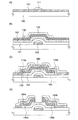
第1の方法は、基板50上にスパッタリング法や蒸着法等の公知の方法により、導電層51を全面に形成し、その後、マスクとなる絶縁層52を液滴吐出手段53により形成する(図1(A)参照)。次に、絶縁層52をマスクとして、導電層51をエッチングして、導電層55を形成する(図1(C)参照)。その後、絶縁層52は除去しない。
第2の方法は、基板50上に液滴吐出手段53により、導電層54を一部の領域に形成し、その後、マスクとなる絶縁層52を液滴吐出手段53により形成する(図1(B)参照)。次に、絶縁層52をマスクとして、導電層54をエッチングして、導電層55を形成する(図1(C)参照)。その後、絶縁層52は除去しない。
In the first method, the
In the second method, the
第3の方法は、基板50上にスパッタリング法等の公知の方法により、導電層51を全面に形成し、その後、マスクとなる絶縁層52を液滴吐出手段53により形成する(図2(A)参照)。次に、フォトマスク56を用いて露光し(図2(B)参照)、現像処理を行って、絶縁層57を形成する(図2(C)参照)。最後に、絶縁層57をマスクとして、導電層51をエッチングして、導電層58を形成する(図2(G)参照)。その後、絶縁層57は除去しない。
第4の方法は、基板50上に液滴吐出手段53により、導電層54を一部の領域に形成し、その後、マスクとなる絶縁層52を液滴吐出手段53により形成する(図2(D)参照)。次に、フォトマスク56を用いて露光し(図2(E)参照)、現像処理を行って、絶縁層57を形成する(図2(F)参照)。最後に、絶縁層57をマスクとして、導電層54をエッチングして、導電層58を形成する(図2(G)参照)。その後、絶縁層57は除去しない。
In the third method, the
In the fourth method, the
なお、上記の第1の方法と第4の方法において、導電層51を半導体層に置換してもよい。この場合、除去しなかった絶縁層52、57は、ゲート絶縁膜として活用することができる。
Note that in the first method and the fourth method, the
また、上記の記載において、導電層を液滴吐出法により形成する場合は、銀、金、銅又はインジウム錫酸化物から形成することを特徴とする。さらに、マスクとなる絶縁層は、有機材料又は珪素と酸素との結合で骨格構造が形成された材料で形成することを特徴とする。 In the above description, in the case where the conductive layer is formed by a droplet discharge method, the conductive layer is formed using silver, gold, copper, or indium tin oxide. Further, the insulating layer serving as a mask is formed of an organic material or a material in which a skeleton structure is formed by a bond of silicon and oxygen.
本発明の薄膜トランジスタの作製方法は、第1の導電層に接する第1のマスクを液滴吐出法により形成するステップ、前記第1のマスクを用いて、前記第1の導電層をエッチングして、第2の導電層を形成するステップを有する。上記ステップを経て、ゲート電極として機能する第2の導電層が完成する。
次に、第1のマスク上に、絶縁層、第1の半導体層及び一導電型が付与された第2の半導体層を積層形成するステップ、前記第2の半導体層に接する第2のマスクを液滴吐出法により形成するステップ、前記第2のマスクを用いて、前記第1及び前記第2の半導体層を同時にエッチングして、第3の半導体層及び一導電型が付与された第4の半導体層を形成するステップを有する。上記ステップを経て、ゲート絶縁膜として機能する絶縁層、活性層として機能する第3の半導体層が完成する。
次に、第4の半導体層に接する第3の導電層を形成するステップ、前記第3の導電層に接する第3のマスクを液滴吐出法により形成するステップ、前記第3のマスクを用いて、前記第4の半導体層及び前記第3の導電層を同時にエッチングするステップを有する。上記ステップを経て、第3の導電層がエッチングされ、ソース・ドレイン配線が完成する。また、第4の半導体層がエッチングされ、ソース・ドレイン配線と活性層(第3の半導体層)を電気的に接続し、一導電型が付与された半導体層が完成する。また、上記ステップを経て、チャネルエッチ型の薄膜トランジスタが完成する。
なお、本発明では、上記ステップにおいて、第1乃至第3のマスクから選択された1つ又は複数は除去しないことを特徴とする。上記特徴により、作製時間の短縮及び作製費用の低減を実現する。
In the method for manufacturing a thin film transistor of the present invention, a step of forming a first mask in contact with the first conductive layer by a droplet discharge method, the first conductive layer is etched using the first mask, Forming a second conductive layer. Through the above steps, a second conductive layer functioning as a gate electrode is completed.
Next, a step of stacking an insulating layer, a first semiconductor layer, and a second semiconductor layer having one conductivity type over the first mask, and a second mask in contact with the second semiconductor layer are formed. Forming by a droplet discharge method; using the second mask, simultaneously etching the first and second semiconductor layers to provide a third semiconductor layer and a fourth conductivity type imparted with one conductivity type; Forming a semiconductor layer. Through the above steps, an insulating layer functioning as a gate insulating film and a third semiconductor layer functioning as an active layer are completed.
Next, a step of forming a third conductive layer in contact with the fourth semiconductor layer, a step of forming a third mask in contact with the third conductive layer by a droplet discharge method, and using the third mask And etching the fourth semiconductor layer and the third conductive layer simultaneously. Through the above steps, the third conductive layer is etched to complete the source / drain wiring. Further, the fourth semiconductor layer is etched, and the source / drain wiring and the active layer (third semiconductor layer) are electrically connected to complete a semiconductor layer imparted with one conductivity type. Through the above steps, a channel-etched thin film transistor is completed.
In the present invention, in the above step, one or more selected from the first to third masks are not removed. With the above features, manufacturing time can be shortened and manufacturing cost can be reduced.
本発明の薄膜トランジスタの作製方法は、第1の導電層に接する第1のマスクを液滴吐出法により形成するステップ、前記第1のマスクを用いて、前記第1の導電層をエッチングして、第2の導電層を形成するステップを有する。上記ステップを経て、ゲート電極として機能する第2の導電層が完成する。
次に、第1のマスク上に、第1の絶縁層、第1の半導体層及び第2の絶縁層を積層形成するステップ、前記第2の絶縁層に接する第2のマスクを液滴吐出法により形成するステップ、前記第2のマスクを用いて、前記第2の絶縁層をエッチングして、第3の絶縁層を形成するステップを有する。上記ステップを経て、ゲート絶縁膜として機能する第1の絶縁層が完成する。また、チャネル保護層として機能する第3の絶縁層が完成する。
次に、第2のマスク上に、一導電型が付与された第2の半導体層を形成するステップ、前記第2の半導体層に接する第3のマスクを液滴吐出法により形成するステップ、前記第3のマスクを用いて、前記第1及び前記第2の半導体層を同時にエッチングして、第3の半導体層及び一導電型が付与された第4の半導体層を形成するステップを有する。上記ステップを経て、活性層として機能する第3の半導体層が完成する。
次に、第4の半導体層と接する第3の導電層を形成するステップ、前記第3の導電層に接する第4のマスクを液滴吐出法により形成するステップ、前記第4のマスクを用いて、前記第4の半導体層及び前記第3の導電層を同時にエッチングするステップを有する。上記ステップを経て、第3の導電層がエッチングされ、ソース・ドレイン配線が完成する。また、第4の半導体層がエッチングされ、ソース・ドレイン配線と活性層(第3の半導体層)を電気的に接続し、一導電型が付与された半導体層が完成する。また、上記ステップを経て、チャネル保護型の薄膜トランジスタが完成する。
なお、本発明では、上記ステップにおいて、第1乃至第4のマスクから選択された1つ又は複数は除去しないことを特徴とする。上記特徴により、作製時間の短縮及び作製費用の低減を実現する。
In the method for manufacturing a thin film transistor of the invention, a step of forming a first mask in contact with the first conductive layer by a droplet discharge method, the first conductive layer is etched using the first mask, Forming a second conductive layer. Through the above steps, a second conductive layer functioning as a gate electrode is completed.
Next, a step of stacking and forming a first insulating layer, a first semiconductor layer, and a second insulating layer over the first mask, and a second mask in contact with the second insulating layer is formed by a droplet discharge method. And forming a third insulating layer by etching the second insulating layer using the second mask. Through the above steps, a first insulating layer functioning as a gate insulating film is completed. In addition, a third insulating layer functioning as a channel protective layer is completed.
Next, a step of forming a second semiconductor layer imparted with one conductivity type over the second mask, a step of forming a third mask in contact with the second semiconductor layer by a droplet discharge method, Using the third mask, the first and second semiconductor layers are simultaneously etched to form a third semiconductor layer and a fourth semiconductor layer imparted with one conductivity type. Through the above steps, a third semiconductor layer functioning as an active layer is completed.
Next, a step of forming a third conductive layer in contact with the fourth semiconductor layer, a step of forming a fourth mask in contact with the third conductive layer by a droplet discharge method, and using the fourth mask And etching the fourth semiconductor layer and the third conductive layer simultaneously. Through the above steps, the third conductive layer is etched to complete the source / drain wiring. Further, the fourth semiconductor layer is etched, and the source / drain wiring and the active layer (third semiconductor layer) are electrically connected to complete a semiconductor layer imparted with one conductivity type. Through the above steps, a channel protective thin film transistor is completed.
In the present invention, in the above step, one or more selected from the first to fourth masks are not removed. With the above features, manufacturing time can be shortened and manufacturing cost can be reduced.
本発明の薄膜トランジスタの作製方法は、第1の半導体層に接する第1のマスクを液滴吐出法により形成するステップ、前記第1のマスクを用いて、前記第1の半導体層をエッチングして、第2の半導体層を形成するステップを有する。上記ステップを経て、活性層となる第2の半導体層が完成する。
次に、第1のマスク上に、導電層を形成するステップ、前記導電層に接する第2のマスクを液滴吐出法により形成するステップ、前記第2のマスクを用いて、前記導電層をエッチングするステップを有する。上記ステップを経て、前記導電層がエッチングされ、ゲート電極が完成する。また、上記ステップを経て、順スタガ型の薄膜トランジスタが完成する。
なお、本発明では、上記ステップにおいて、第1及び第2のマスクから選択された1つ又は複数は除去しないことを特徴とする。上記特徴により、作製時間の短縮及び作製費用の低減を実現する。
The method for manufacturing a thin film transistor of the present invention includes a step of forming a first mask in contact with a first semiconductor layer by a droplet discharge method, etching the first semiconductor layer using the first mask, Forming a second semiconductor layer. Through the above steps, a second semiconductor layer that becomes an active layer is completed.
Next, a step of forming a conductive layer on the first mask, a step of forming a second mask in contact with the conductive layer by a droplet discharge method, and etching the conductive layer using the second mask There is a step to do. Through the above steps, the conductive layer is etched to complete the gate electrode. Further, through the above steps, a forward staggered thin film transistor is completed.
In the present invention, in the above step, one or more selected from the first and second masks are not removed. With the above features, manufacturing time can be shortened and manufacturing cost can be reduced.
本発明の薄膜トランジスタの作製方法は、第1の導電層、一導電型が付与された第1の半導体層を積層形成するステップ、前記第1の半導体層に接する第1のマスクを液滴吐出法により形成するステップ、前記第1のマスクを用いて、前記第1の半導体層をエッチングして、一導電型が付与された第2の半導体層を形成するステップを有する。上記ステップを経て、ソース・ドレイン配線となる第1の導電層が完成する。
次に、前記第2の半導体層に接する第3の半導体層を形成するステップ、前記第3の半導体層に接する第2のマスクを液滴吐出法により形成するステップ、前記第2のマスクを用いて、前記第2及び前記第3の半導体層をエッチングして、一導電型が付与された第4の半導体層と、第5の半導体層を形成するステップを有する。上記のステップを経て、活性層となる第5の半導体層が完成する。また、ソース・ドレイン配線と、活性層(第5の半導体層)とを電気的に接続する、一導電型が付与された第4の半導体層が完成する。
次に、前記第2のマスク上に、絶縁層、第2の導電層を積層形成するステップ、前記第2の導電層に接する第3のマスクを液滴吐出法により形成するステップ、前記第3のマスクを用いて、前記第2の導電層をエッチングするステップを有する。上記ステップを経て、ゲート絶縁膜として機能する絶縁層が完成し、また、前記第2の導電層をエッチングして、ゲート電極が完成する。
なお、本発明では、上記ステップにおいて、第1乃至第3のマスクから選択された1つ又は複数は除去しないことを特徴とする。上記特徴により、作製時間の短縮及び作製費用の低減を実現する。
The method for manufacturing a thin film transistor of the present invention includes a step of stacking a first conductive layer, a first semiconductor layer imparted with one conductivity type, and a droplet discharge method using a first mask in contact with the first semiconductor layer. And forming a second semiconductor layer imparted with one conductivity type by etching the first semiconductor layer using the first mask. Through the above steps, the first conductive layer to be the source / drain wiring is completed.
Next, forming a third semiconductor layer in contact with the second semiconductor layer, forming a second mask in contact with the third semiconductor layer by a droplet discharge method, and using the second mask And etching the second and third semiconductor layers to form a fourth semiconductor layer imparted with one conductivity type and a fifth semiconductor layer. Through the above steps, a fifth semiconductor layer to be an active layer is completed. In addition, a fourth semiconductor layer imparted with one conductivity type, which electrically connects the source / drain wiring and the active layer (fifth semiconductor layer), is completed.
Next, a step of laminating and forming an insulating layer and a second conductive layer on the second mask, a step of forming a third mask in contact with the second conductive layer by a droplet discharge method, the third And etching the second conductive layer using the mask. Through the above steps, an insulating layer functioning as a gate insulating film is completed, and the second conductive layer is etched to complete a gate electrode.
In the present invention, in the above step, one or more selected from the first to third masks are not removed. With the above features, manufacturing time can be shortened and manufacturing cost can be reduced.
本発明の薄膜トランジスタの作製方法は、第1の半導体層に接する第1のマスクを液滴吐出法により形成するステップ、前記第1のマスクを用いて、前記第1の半導体層をエッチングして、第2の半導体層を形成するステップを有する。上記ステップを経て、活性層となる第2の半導体層が完成する。
次に、第2の半導体層上に、一導電型が付与された第3の半導体層、第1の導電層を積層形成するステップ、前記第1の導電層に接する第2のマスクを液滴吐出法により形成するステップ、前記第2のマスクを用いて、前記第3の半導体層及び前記第1の導電層をエッチングして、一導電型が付与された第4の半導体層と第2の導電層を形成するステップを有する。上記ステップを経て、ソース・ドレイン配線となる第2の導電層、ソース・ドレイン配線と活性層(第2の半導体層)を電気的に接続する、一導電型が付与された第4の半導体層が完成する。
次に、前記第2のマスク上に、絶縁層、第3の導電層を積層形成するステップ、前記第3の導電層に接する第3のマスクを液滴吐出法により形成するステップ、前記第3のマスクを用いて、前記第3の導電層をエッチングするステップを有することを特徴とする。上記ステップを経て、ゲート絶縁膜として機能する絶縁層が完成する。また、第3の導電層をエッチングして、ゲート電極が完成する。
なお、本発明では、上記ステップにおいて、第1乃至第3のマスクから選択された1つ又は複数は除去しないことを特徴とする。上記特徴により、作製時間の短縮及び作製費用の低減を実現する。
The method for manufacturing a thin film transistor of the present invention includes a step of forming a first mask in contact with a first semiconductor layer by a droplet discharge method, etching the first semiconductor layer using the first mask, Forming a second semiconductor layer. Through the above steps, a second semiconductor layer that becomes an active layer is completed.
Next, a step of stacking and forming a third semiconductor layer imparted with one conductivity type on the second semiconductor layer, the first conductive layer, and a second mask in contact with the first conductive layer as a droplet A step of forming by a discharge method, the third semiconductor layer and the first conductive layer are etched using the second mask, and the fourth semiconductor layer provided with one conductivity type and the second semiconductor layer Forming a conductive layer. Through the above steps, a second conductive layer serving as a source / drain wiring, a fourth semiconductor layer imparted with one conductivity type, which electrically connects the source / drain wiring and the active layer (second semiconductor layer). Is completed.
Next, a step of laminating and forming an insulating layer and a third conductive layer on the second mask, a step of forming a third mask in contact with the third conductive layer by a droplet discharge method, the third And etching the third conductive layer using the mask. Through the above steps, an insulating layer functioning as a gate insulating film is completed. In addition, the third conductive layer is etched to complete the gate electrode.
In the present invention, in the above step, one or more selected from the first to third masks are not removed. With the above features, manufacturing time can be shortened and manufacturing cost can be reduced.
上述した作製方法のうち、導電層は、液滴吐出法、スパッタリング法又は蒸着法により形成することを特徴とする。また、液滴吐出法で形成する場合は、銀、金、銅又はインジウム錫酸化物から形成することを特徴とする。マスクは、液滴吐出法により形成された絶縁層をそのまま用いるか、又は、液滴吐出法により形成された絶縁層に、フォトマスクを用いた露光処理及び現像処理を行って形成する。さらに、それらのマスクは、有機材料又は珪素と酸素との結合で骨格構造が形成された材料で形成することを特徴とする。 Of the above-described manufacturing methods, the conductive layer is formed by a droplet discharge method, a sputtering method, or an evaporation method. Further, when formed by a droplet discharge method, it is formed from silver, gold, copper, or indium tin oxide. As the mask, an insulating layer formed by a droplet discharge method is used as it is, or an insulating layer formed by a droplet discharge method is formed by performing exposure processing and development processing using a photomask. Further, these masks are formed using an organic material or a material in which a skeleton structure is formed by a bond of silicon and oxygen.
本発明により、剥離工程を用いずに、工程を簡略化して、作製時間の短縮及び作製費用の低減を実現した薄膜トランジスタの作製方法、半導体装置の作製方法を提供することができる。 According to the present invention, it is possible to provide a method for manufacturing a thin film transistor and a method for manufacturing a semiconductor device in which a manufacturing process is shortened and manufacturing cost is reduced without using a peeling process.
本発明の実施の形態について、図面を用いて詳細に説明する。但し、本発明は以下の説明に限定されず、本発明の趣旨及びその範囲から逸脱することなくその形態及び詳細を様々に変更し得ることは当業者であれば容易に理解される。従って、本発明は以下に示す実施の形態の記載内容に限定して解釈されるものではない。なお、以下に説明する本発明の構成において、同じものを指す符号は異なる図面間で共通して用いる。
(実施の形態1)
Embodiments of the present invention will be described in detail with reference to the drawings. However, the present invention is not limited to the following description, and it is easily understood by those skilled in the art that modes and details can be variously changed without departing from the spirit and scope of the present invention. Therefore, the present invention should not be construed as being limited to the description of the embodiments below. Note that in the structures of the present invention described below, the same reference numerals are used in common in different drawings.
(Embodiment 1)
本発明の薄膜トランジスタの作製方法について、図3を用いて説明する。ここでは、非晶質半導体をチャネル部とした、チャネルエッチ型の薄膜トランジスタの作製方法について説明する。 A method for manufacturing the thin film transistor of the present invention will be described with reference to FIGS. Here, a method for manufacturing a channel-etched thin film transistor using an amorphous semiconductor as a channel portion is described.
基板100としては、バリウムホウケイ酸ガラス、アルミノホウケイ酸ガラス等からなるガラス基板、石英基板、シリコン基板、金属基板、ステンレス基板又は本作製工程の処理温度に耐えうる耐熱性を有するプラスチック基板を用いる(図3(A)参照)。そして、基板100上に、第1の導電層101を形成する。第1の導電層101は、液滴吐出法、蒸着法、イオンプレーティング法、スパッタリング法、CVD法、めっき法等の公知の方法により形成する。なお、第1の導電層101は、被処理物の全面に形成してもよいし、液滴吐出法により一部の領域のみに形成してもよい。次に、第1の導電層101に接するように、液滴吐出法により第1のマスク111を形成する。
As the
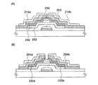
第1のマスク111を用いて、第1の導電層101をエッチングして、第2の導電層102を形成する(図3(B)参照)。第2の導電層102は、ゲート電極として機能する。続いて、第1のマスク111は除去せず、該第1のマスク111上に、絶縁層121、第1の半導体層131、一導電型が付与された第2の半導体層132を積層形成する。絶縁層121はゲート絶縁膜として機能するものであり、プラズマCVD法等の公知の方法を用いて、珪素の酸化膜、窒化膜を単層又は積層構造で形成する。第1の半導体層131は活性層として機能するものであり、プラズマCVD法、スパッタリング法等の公知の方法を用いて形成する。また、第1の半導体層131は、非晶質半導体又は微結晶半導体で形成する。第2の半導体層132は、一導電型が付与され、シランガスとフォスフィンガスを用いて形成したり、CVD法により半導体層を形成後に、ドーピング法により不純物元素を添加して形成したりする。次に、第2の半導体層132に接する第2のマスク112を液滴吐出法により形成する。
The first
続いて、第2のマスク112を用いて、第1の半導体層131と、一導電型が付与された第2の半導体層132を同時にエッチングして、第3の半導体層133と、一導電型が付与された第4の半導体層134を形成する(図3(C)参照)。その後、本プロセスでは、第2のマスク112を除去するが、除去せずに残しておいてもよい。除去しない場合には、さらなる作製時間の短縮及び作製費用の低減が実現する。次に、第4の半導体層134に接する第3の導電層103を形成する。第3の導電層103は、液滴吐出法、蒸着法等の公知の方法により形成する。なお、第3の導電層103は、全面に形成してもよいし、液滴吐出法により一部に形成してもよい。なお、第2のマスク112を除去しない場合、第3の半導体層133及び第4の半導体層134と、第3の導電層103とは、端部122でのみ電気的に接続する。次に、第3の導電層103に接する第3のマスク113a、113bを液滴吐出法により形成する。
Subsequently, using the
次に、第3のマスク113a、113bを用いて、第3の導電層103と第4の半導体層134を同時にエッチングして、第4の導電層104a、104b、第5の半導体層135a、135bを形成する(図3(D)参照)。このエッチング処理を経ると、図示するように、第3の半導体層133も少しエッチングされる。上記工程を経て、チャネルエッチ型の薄膜トランジスタが完成する。
Next, the third
本発明は、第1のマスク111、第2のマスク112、第3のマスク113a、113bを液滴吐出法により形成することを特徴とする。また、これらのマスクのうち、少なくとも1つのマスクは、除去せずに残しておくことを特徴とする。第1のマスク111、第2のマスク112、第3のマスク113a、113bは、液滴吐出法により形成した絶縁層をそのままマスクとして用いるか、又は液滴吐出法で形成された絶縁層に露光・現像・エッチング処理を行った絶縁層をマスクとして用いる。さらに、好ましくは、第1の導電層101と第3の導電層103も液滴吐出法により形成することを特徴とする。
The present invention is characterized in that the
なお、ここでは、基板上に薄膜トランジスタが完成した状態をTFT基板(トランジスタ基板)とよぶ。つまり、上記工程を経ると、TFT基板が完成した状態となる。 Here, a state where a thin film transistor is completed on a substrate is referred to as a TFT substrate (transistor substrate). That is, after the above steps, the TFT substrate is completed.
なお、液滴吐出法において用いるノズルの径は、0.02〜100μm(好適には30μm以下)に設定し、該ノズルから吐出される組成物の吐出量は0.001pl〜100pl(好適には10pl以下)に設定するとよい。この吐出量は、ノズルの径の大きさに比例して増加する。但し、ノズルの径は、形成するパターンの形状やその大きさに従って適宜変更するとよい。また、被処理物とノズルの吐出口との距離は、所望の箇所に滴下するために、出来る限り近づけておくことが好ましく、好適には0.1〜3mm(好適には1mm以下)程度に設定する。ノズルと被処理物は、その相対的な距離を保ちながら、該ノズル又は該被処理物が移動して、所望のパターンを描画する。 The diameter of the nozzle used in the droplet discharge method is set to 0.02 to 100 μm (preferably 30 μm or less), and the discharge amount of the composition discharged from the nozzle is 0.001 pl to 100 pl (preferably 10 pl or less). This discharge amount increases in proportion to the size of the nozzle diameter. However, the nozzle diameter may be appropriately changed according to the shape of the pattern to be formed and its size. In addition, the distance between the object to be processed and the nozzle outlet is preferably as close as possible in order to drop it at a desired location, preferably about 0.1 to 3 mm (preferably about 1 mm or less). Set. While maintaining the relative distance between the nozzle and the object to be processed, the nozzle or the object to be processed moves to draw a desired pattern.
液滴吐出法でマスクを形成する際、吐出口から吐出する組成物は、絶縁性材料を溶媒に溶解又は分散させたものを用いる。絶縁性材料とは、エポキシ樹脂、アクリル樹脂、フェノール樹脂、ノボラック樹脂、メラミン樹脂、ウレタン樹脂等の樹脂材料を用いる。なおこれらの樹脂材料を用いる場合、その粘度は、溶媒を用いて溶解又は分散することで調整するとよい。また、撥液性の材料として、フッ素原子が含まれた樹脂、あるいは炭化水素のみで構成された樹脂が挙げられる。より詳しくは、分子内にフッ素原子を含有するモノマーを含む樹脂、或いは全て炭素と水素原子のみから構成されるモノマーを含む樹脂が挙げられる。また、アクリル、ベンゾシクロブテン、パリレン、フレア、透過性を有するポリイミドなどの有機材料、シロキサン系ポリマー等の重合によってできた化合物材料、水溶性ホモポリマーと水溶性共重合体を含む組成物等が挙げられる。 When forming a mask by a droplet discharge method, a composition in which an insulating material is dissolved or dispersed in a solvent is used as the composition discharged from the discharge port. As the insulating material, a resin material such as an epoxy resin, an acrylic resin, a phenol resin, a novolac resin, a melamine resin, or a urethane resin is used. In addition, when using these resin materials, the viscosity is good to adjust by melt | dissolving or disperse | distributing using a solvent. In addition, examples of the liquid repellent material include a resin containing a fluorine atom, or a resin composed of only a hydrocarbon. More specifically, a resin containing a monomer containing a fluorine atom in the molecule, or a resin containing a monomer composed entirely of carbon and hydrogen atoms can be given. Also, organic materials such as acrylic, benzocyclobutene, parylene, flare, permeable polyimide, compound materials made by polymerization of siloxane polymers, compositions containing water-soluble homopolymers and water-soluble copolymers, etc. Can be mentioned.
有機材料を用いると、その平坦性が優れているため、後に導電体を成膜した際にも、段差部で膜厚が極端に薄くなったり、断線が起こったりすることがなく、好適である。但し、有機材料は、脱ガス発生の防止のため、下層と上層に、珪素を含む無機材料で薄膜を形成するとよい。具体的には、プラズマCVD法やスパッタリング法により、窒化酸化珪素膜や窒化珪素膜を形成するとよい。シロキサン系ポリマーは、珪素と酸素との結合で骨格構造が構成され置換基に少なくとも水素を含む材料、又は、置換基にフッ素、アルキル基、または芳香族炭化水素のうち少なくとも1種を有する材料の代表例として挙げたものであり、上記条件の範疇にある様々な材料を用いることができる。このシロキサン系ポリマーは、平坦性に優れており、また透明性や耐熱性をも有し、シロキサンポリマーからなる絶縁体を形成後に300度〜600度程度以下の温度で加熱処理を行うことができるという利点を有する。この加熱処理により、例えば水素化と焼成の処理を同時に行うことができる。 When an organic material is used, the flatness thereof is excellent, and therefore, even when a conductor is formed later, the film thickness is not extremely reduced at the stepped portion, and disconnection does not occur. . However, for the organic material, a thin film is preferably formed of an inorganic material containing silicon in a lower layer and an upper layer in order to prevent outgassing. Specifically, a silicon nitride oxide film or a silicon nitride film is preferably formed by a plasma CVD method or a sputtering method. A siloxane-based polymer is a material having a skeleton structure formed of a bond of silicon and oxygen and containing at least hydrogen as a substituent, or a material having at least one of fluorine, an alkyl group, or an aromatic hydrocarbon as a substituent. These are given as representative examples, and various materials within the above conditions can be used. This siloxane-based polymer is excellent in flatness, has transparency and heat resistance, and can be heat-treated at a temperature of about 300 ° C. to 600 ° C. or less after forming an insulator made of a siloxane polymer. Has the advantage. By this heat treatment, for example, hydrogenation and baking treatment can be performed simultaneously.
また、感光剤を含む市販のレジスト材料を用いてもよく、例えば、代表的なポジ型レジストである、ノボラック樹脂と感光剤であるナフトキノンジアジド化合物、ネガ型レジストであるベース樹脂、ジフェニルシランジオール及び酸発生剤などを、溶媒に溶解又は分散させたものを用いてもよい。その粘度は、溶媒を用いて、上記の材料を溶解又は分散することで調節するとよい。 Further, a commercially available resist material containing a photosensitizer may be used. For example, a novolak resin that is a typical positive resist and a naphthoquinonediazide compound that is a photosensitizer, a base resin that is a negative resist, diphenylsilanediol, and You may use what dissolved or disperse | distributed the acid generator etc. in the solvent. The viscosity may be adjusted by dissolving or dispersing the above material using a solvent.
一方、液滴吐出法で導電層を形成する際、吐出口から吐出する組成物は、導電性材料を溶媒に溶解又は分散させたものを用いる。導電性材料とは、Ag(銀)、Au(金)、Cu(銅)、Ni(ニッケル)、Pt(白金)、Pd(鉛)、Ir(イリジウム)、Rh(ロジウム)、W(タングステン)、Al(アルミニウム)等の金属、Cd(カドミウム)、Zn(亜鉛)、Fe(鉄)、Ti(チタン)、Si(珪素)、Ge(ゲルマニウム)、Zr(ジルコニウム)、Ba(バリウム)、ハロゲン化銀の微粒子又は分散性ナノ粒子に相当する。また、透明導電膜として用いられるインジウム錫酸化物(ITO)、インジウム錫酸化物と酸化珪素からなるITSO、有機インジウム、有機スズ、酸化亜鉛、窒化チタン等に相当する。但し、吐出口から吐出する組成物は、比抵抗値を考慮して、金、銀、銅のいずれかの材料を溶媒に溶解又は分散させたものを用いることが好適であり、より好適には、低抵抗な銀、銅を用いるとよい。但し、銀、銅を用いる場合には、不純物対策のため、合わせてバリア膜を設けるとよい。 On the other hand, when forming a conductive layer by a droplet discharge method, a composition in which a conductive material is dissolved or dispersed in a solvent is used as a composition discharged from a discharge port. The conductive material is Ag (silver), Au (gold), Cu (copper), Ni (nickel), Pt (platinum), Pd (lead), Ir (iridium), Rh (rhodium), W (tungsten). , Metals such as Al (aluminum), Cd (cadmium), Zn (zinc), Fe (iron), Ti (titanium), Si (silicon), Ge (germanium), Zr (zirconium), Ba (barium), halogen Corresponds to silver halide fine particles or dispersible nanoparticles. Further, it corresponds to indium tin oxide (ITO) used as a transparent conductive film, ITSO composed of indium tin oxide and silicon oxide, organic indium, organic tin, zinc oxide, titanium nitride, and the like. However, it is preferable to use a composition in which any of gold, silver and copper is dissolved or dispersed in a solvent in consideration of the specific resistance value, more preferably the composition discharged from the discharge port. It is preferable to use low resistance silver or copper. However, when silver or copper is used, a barrier film may be provided as a countermeasure against impurities.
溶媒は、酢酸ブチル、酢酸エチル等のエステル類、イソプロピルアルコール、エチルアルコール等のアルコール類、メチルエチルケトン、アセトン等の有機溶剤等に相当する。組成物の粘度は50cp以下が好適であり、これは、乾燥が起こることを防止したり、吐出口から組成物を円滑に吐出できるようにしたりするためである。また、組成物の表面張力は、40mN/m以下が好適である。なお、用いる溶媒や、用途に合わせて、組成物の粘度等は適宜調整するとよい。一例として、ITOや、有機インジウム、有機スズ、銀、金を溶媒に溶解又は分散させた組成物の粘度は5〜20mPa・Sに設定する。 The solvent corresponds to esters such as butyl acetate and ethyl acetate, alcohols such as isopropyl alcohol and ethyl alcohol, organic solvents such as methyl ethyl ketone and acetone. The viscosity of the composition is preferably 50 cp or less, in order to prevent the drying from occurring or to smoothly discharge the composition from the discharge port. The surface tension of the composition is preferably 40 mN / m or less. Note that the viscosity of the composition and the like may be appropriately adjusted according to the solvent to be used and the application. As an example, the viscosity of a composition in which ITO, organic indium, organic tin, silver, or gold is dissolved or dispersed in a solvent is set to 5 to 20 mPa · S.
また、被処理物の表面にプラズマ処理を施してもよい。これは、プラズマ処理を施すと、被処理物の表面が親水性になったり、疎液性になったりすることを活用するためである。例えば、純水に対しては親水性になり、アルコールを溶媒したペーストに対しては疎液性になる。 Moreover, you may plasma-process on the surface of a to-be-processed object. This is to take advantage of the fact that the surface of the workpiece becomes hydrophilic or lyophobic when the plasma treatment is performed. For example, it becomes hydrophilic with respect to pure water and becomes lyophobic with respect to a paste using an alcohol as a solvent.
組成物を吐出する工程は、減圧下で行うと、組成物を吐出して被処理物に着弾するまでの間に、該組成物の溶媒が揮発し、後の乾燥と焼成の工程を省略、又は短くすることができるため、好適である。また、組成物を吐出して絶縁層を形成した後は、乾燥と焼成の一方又は両方の工程を行う。乾燥と焼成の工程は、両工程とも加熱処理の工程であるが、例えば、乾燥は100度で3分間、焼成は200〜350度で15分間〜120分間で行うもので、その目的、温度と時間が異なるものである。乾燥の工程、焼成の工程は、常圧下又は減圧下で、レーザ光の照射や瞬間熱アニール、加熱炉などにより行う。なお、この加熱処理を行うタイミングは特に限定されない。乾燥と焼成の工程を良好に行うためには、基板を加熱しておいてもよく、そのときの温度は、基板等の材質に依存するが、一般的には100〜800度(好ましくは200〜350度)とする。本工程により、組成物中の溶媒の揮発、又は化学的に分散剤を除去するとともに、周囲の樹脂が硬化収縮することで、融合と融着を加速する。 When the step of discharging the composition is performed under reduced pressure, the solvent of the composition is volatilized before discharging the composition and landing on the object to be processed, and the subsequent drying and baking steps are omitted. Alternatively, it can be shortened, which is preferable. In addition, after forming the insulating layer by discharging the composition, one or both of drying and baking steps are performed. The drying and firing steps are both heat treatment steps. For example, the drying is performed at 100 degrees for 3 minutes, and the firing is performed at 200 to 350 degrees for 15 minutes to 120 minutes. Time is different. The drying process and the firing process are performed under normal pressure or reduced pressure by laser light irradiation, rapid thermal annealing, a heating furnace, or the like. In addition, the timing which performs this heat processing is not specifically limited. In order to satisfactorily perform the drying and firing steps, the substrate may be heated, and the temperature at that time depends on the material of the substrate or the like, but is generally 100 to 800 degrees (preferably 200). ~ 350 degrees). By this step, the solvent in the composition is volatilized or the dispersant is chemically removed, and the surrounding resin is cured and contracted to accelerate fusion and fusion.
レーザ光の照射は、連続発振またはパルス発振の気体レーザ又は固体レーザを用いれば良い。前者の気体レーザとしては、エキシマレーザ、YAGレーザ等が挙げられ、後者の固体レーザとしては、Cr、Nd等がドーピングされたYAG、YVO4等の結晶を使ったレーザ等が挙げられる。なお、レーザ光の吸収率の関係から、連続発振のレーザを用いることが好ましい。また、パルス発振と連続発振を組み合わせたハイブリッドのレーザ照射方法を用いてもよい。但し、基板100の耐熱性に依っては、レーザ光の照射による加熱処理は、該基板100が破壊しないように、数マイクロ秒から数十秒の間で瞬間に行うとよい。瞬間熱アニール(RTA)は、不活性ガスの雰囲気下で、紫外光乃至赤外光を照射する赤外ランプやハロゲンランプなどを用いて、急激に温度を上昇させ、数分〜数マイクロ秒の間で瞬間的に熱を加えて行う。この処理は瞬間的に行うために、実質的に最表面の薄膜のみを加熱することができ、下層の膜には影響を与えない。つまり、プラスチック基板等の耐熱性が弱い基板にも影響を与えない。
For the laser light irradiation, a continuous wave or pulsed gas laser or solid-state laser may be used. Examples of the former gas laser include an excimer laser and a YAG laser, and examples of the latter solid-state laser include a laser using a crystal such as YAG or YVO 4 doped with Cr, Nd, or the like. Note that it is preferable to use a continuous wave laser because of the absorption rate of the laser light. Alternatively, a hybrid laser irradiation method combining pulse oscillation and continuous oscillation may be used. However, depending on the heat resistance of the
なお、液滴吐出法には、オンデマンド型とコンティニュアス型の2つの方式があるが、どちらの方式を用いてもよい。また液滴吐出法において用いるヘッドには大別して、圧電方式、加熱方式があるが、本発明では、どちらの方法を用いてもよい。圧電方式は圧電体の電圧印加により変形する性質を利用したものであり、加熱方式はノズル内に設けられたヒータにより組成物を沸騰させ、該組成物を吐出するものである。
(実施の形態2)
There are two types of droplet discharge methods, an on-demand type and a continuous type, and either method may be used. The head used in the droplet discharge method is roughly classified into a piezoelectric method and a heating method, but either method may be used in the present invention. The piezoelectric method utilizes the property of being deformed by applying a voltage to a piezoelectric body, and the heating method is a method in which a composition is boiled by a heater provided in a nozzle and the composition is discharged.
(Embodiment 2)
本発明の薄膜トランジスタの作製方法について、図4、5を用いて説明する。ここでは、非晶質半導体をチャネル部とした、チャネル保護型の薄膜トランジスタの作製方法について説明する。 A method for manufacturing the thin film transistor of the present invention will be described with reference to FIGS. Here, a method for manufacturing a channel protective thin film transistor using an amorphous semiconductor as a channel portion will be described.
基板200としては、ガラス基板、石英基板、シリコン基板又は本作製工程の処理温度に耐えうる耐熱性を有するプラスチック基板を用いる(図4(A)参照)。そして、基板200上に、第1の導電層201を形成する。第1の導電層201は、液滴吐出法、蒸着法等の公知の方法により形成する。なお、第1の導電層201は、被処理物の全面に形成してもよいし、液滴吐出法により一部の領域のみに形成してもよい。次に、第1の導電層201に接するように、液滴吐出法により第1のマスク211を形成する。
As the
第1のマスク211を用いて、第1の導電層201をエッチングして、第2の導電層202を形成する(図4(B)参照)。第2の導電層202は、ゲート電極として機能する。続いて、第1のマスク211は除去せず、該第1のマスク211上に、第1の絶縁層221、第1の半導体層231、第2の絶縁層222を積層形成する。第1の絶縁層221はゲート絶縁膜として機能するものであり、プラズマCVD法等の公知の方法を用いて、珪素の酸化膜、窒化膜を単層又は積層構造で形成する。第1の半導体層231は活性層として機能するものであり、プラズマCVD法、スパッタリング法等の公知の方法を用いて形成する。また、第1の半導体層231は、非晶質半導体又は微結晶半導体で形成する。次に、第2の絶縁層222に接する第2のマスク212を液滴吐出法により形成する。
The first
第2のマスク212を用いて、第2の絶縁層222をエッチングして、第3の絶縁層223を形成する(図4(C)参照)。第3の絶縁層223は、チャネル保護層として機能する。続いて、第2のマスク212上に、一導電型が付与された第2の半導体層232を形成する。第2の半導体層232は、シランガスとフォスフィンガスを用いて形成したり、CVD法により半導体層を形成後に、ドーピング法により不純物元素を添加して形成したりする。次に、第2の半導体層232に接する第3のマスク213を液滴吐出法により形成する。
The second
第3のマスク213を用いて、第1の半導体層231と第2の半導体層232を同時にエッチングして、第3の半導体層233と第4の半導体層234を形成する(図5(A)参照)。その後、本プロセスでは、第3のマスク213を除去するが、除去せずに残しておいてもよい。除去しない場合には、さらなる作製時間の短縮及び作製費用の低減が実現する。次に、第4の半導体層234に接する第3の導電層203を形成する。第3の導電層203は、液滴吐出法、蒸着法等の公知の方法により形成する。なお、第3の導電層203は、全面に形成してもよいし、液滴吐出法により一部に形成してもよい。なお、第3のマスク213を除去しない場合、第3の半導体層233及び第4の半導体層234と、第3の導電層203とは、端部240でのみ電気的に接続する。次に、第3の導電層203に接する第4のマスク214a、214bを液滴吐出法により形成する。
The
第4のマスク214a、214bを用いて、第4の半導体層234及び第3の導電層203を同時にエッチングして、第5の半導体層235a、235bと、第4の導電層204a、204bを形成する(図5(B)参照)。このエッチング処理の際、第3の半導体層233は、第3の絶縁層223と第2のマスク212に保護され、エッチングされることはない。上記工程を経て、チャネル保護型の薄膜トランジスタが完成する。
Using the
本発明は、第1のマスク211、第2のマスク212、第3のマスク213、第4のマスク214a、214bを液滴吐出法により形成することを特徴とする。また、これらのマスクのうち、少なくとも1つのマスクは、除去せずに残しておくことを特徴とする。第1のマスク211、第2のマスク212、第3のマスク213、第4のマスク214a、214bは、液滴吐出法により形成した絶縁層をそのままマスクとして用いるか、又は液滴吐出法で形成された絶縁層に露光・現像・エッチング処理を行った絶縁層をマスクとして用いる。さらに、好ましくは、第1の導電層201と第3の導電層203も液滴吐出法により形成することを特徴とする。なお、液滴吐出法によるマスクや導電層の形成に関しては、上記の実施の形態1において上述したので、ここではその説明を省略する。
(実施の形態3)
The present invention is characterized in that the
(Embodiment 3)
本発明の薄膜トランジスタの作製方法について、図6、7を用いて説明する。ここでは、順スタガ型の薄膜トランジスタの作製方法について説明する。 A method for manufacturing the thin film transistor of the present invention will be described with reference to FIGS. Here, a method for manufacturing a forward staggered thin film transistor is described.
基板300としては、ガラス基板、石英基板、シリコン基板又は本作製工程の処理温度に耐えうる耐熱性を有するプラスチック基板を用いる(図6(A)参照)。そして、基板300上に、第1の半導体層331を形成する。第1の半導体層331は、スパッタリング法、LPCVD法、プラズマCVD法等の公知の方法により形成し、非晶質半導体、微結晶半導体のいずれでもよい。次いで、図示しないが、前記半導体膜を公知の結晶化法(レーザ結晶化法、RTA又はファーネスアニール炉を用いる熱結晶化法、結晶化を助長する金属元素を用いる熱結晶化法等)を用いて結晶化させる。次に、第1の半導体層331に接するように、液滴吐出法により第1のマスク311を形成する。
As the
第1のマスク311を用いて、第1の半導体層331をエッチングして、第2の半導体層332を形成する(図6(B)参照)。第2の半導体層332は、活性層として機能する。続いて、第1のマスク311を除去せず、該第1のマスク311上に、第1の導電層301を形成する。第1の導電層301は、液滴吐出法、蒸着法等の公知の方法により形成する。なお、第1の導電層301は、全面に形成してもよいし、液滴吐出法により一部に形成してもよい。ここで、第1のマスク311は、ゲート絶縁膜として機能する。次に、第1の導電層301に接するように、液滴吐出法により第2のマスク312を形成する。
The
第2のマスク312を用いて、第1の導電層301をエッチングして、第2の導電層302を形成する(図6(C)参照)。第2の導電層302は、ゲート電極として機能する。続いて、第2のマスク312及び第2の導電層302をマスクとして、第2の半導体層332に燐やボロンなどの不純物元素をドーピング法等により添加して、不純物領域333とチャネル形成領域334を形成する。上記工程を経て、順スタガ型の薄膜トランジスタが完成する。
The first
次に、完成した素子の全面に絶縁層321を形成する(図7(A)参照)。絶縁層321は、液滴吐出法、スピンコート法等の公知の方法により形成する。なお、絶縁層321は、液滴吐出法で形成した場合、表面に凸凹が形成される場合があるため、そのような場合には、公知の平坦化手段、例えばCMP法などにより表面を平坦化しておくとよい。その後、不純物領域333を露出させる開口部を形成するために、絶縁層321に接するように、液滴吐出法により第3のマスク313a〜313cを形成する。
Next, an insulating
第3のマスク313a〜313cを用いて、絶縁層321をエッチングして、開口部322、323を形成する(図7(B)参照)。次に、開口部322、323を充填し、なおかつ不純物領域333に接するように、第3の導電層303a、303bを形成する。これらの導電層は、液滴吐出法、スパッタリング等の公知の方法により形成する。なお、第3の導電層303a、303bをスパッタリング法等で全面に形成した場合は、マスクを用いてエッチングする工程が必要となる。一方、液滴吐出法により形成する場合は、選択的に形成することができるため、後のフォトリソグラフィ工程が不必要となる。但し、液滴吐出法で形成した場合であっても、フォトリソグラフィ工程を用いることで、所望の形状にしてもよい。
The insulating
本発明は、第1のマスク311、第2のマスク312、第3のマスク313a〜313cを液滴吐出法により形成することを特徴とする。また、これらのマスクのうち、少なくとも1つのマスクは、除去せずに残しておくことを特徴とする。第1のマスク311、第2のマスク312、第3のマスク313a〜313cは、液滴吐出法により形成した絶縁層をそのままマスクとして用いるか、又は液滴吐出法で形成された絶縁層に露光・現像・エッチング処理を行った絶縁層をマスクとして用いる。さらに、好ましくは、第1の導電層301と第3の導電層303a、303bも液滴吐出法により形成することを特徴とする。なお、液滴吐出法によるマスクや導電層の形成に関しては、上記の実施の形態1において上述したので、ここではその説明を省略する。
(実施の形態4)
The present invention is characterized in that the
(Embodiment 4)
本発明の薄膜トランジスタの作製方法について、図8を用いて説明する。ここでは、順スタガ型の薄膜トランジスタの作製方法について説明する。 A method for manufacturing the thin film transistor of the present invention will be described with reference to FIGS. Here, a method for manufacturing a forward staggered thin film transistor is described.
基板400としては、ガラス基板、石英基板等を用いる(図8(A)参照)。そして、基板400上に、第1の導電層401a、401bを形成する。第1の導電層401a、401bは、液滴吐出法、蒸着法等の公知の方法により形成する。なお、第1の導電層401a、401bをスパッタリング法等で全面に形成した場合は、マスクを用いてエッチングする工程が必要となる。一方、液滴吐出法により形成する場合は、選択的に形成することができるため、後のフォトリソグラフィ工程が不必要となる。但し、液滴吐出法で形成した場合であっても、フォトリソグラフィ工程を用いることで、所望の形状にしてもよい。続いて、第1の導電層401a、401bに接するように、一導電型が付与された第1の半導体層431を形成する。第1の半導体層431は、シランガスとフォスフィンガスを用いて形成したり、CVD法により半導体層を形成後に、ドーピング法により不純物元素を添加して形成したりする。続いて、第1の半導体層431に接するように、第1のマスク411a、411bを液滴吐出法により形成する。
As the
第1のマスク411a、411bを用いて、第1の半導体層431をエッチングして、第2の半導体層432a、432bを形成する(図8(B)参照)。その後、本プロセスでは、第1のマスク411a、411bを除去するが、除去せずに残しておいてもよい。除去しない場合には、さらなる作製時間の短縮及び作製費用の低減が実現する。次に、第2の半導体層432a、432bを覆うように、第3の半導体層433を形成する。なお、第1のマスク411a、411bを除去しない場合、第2の半導体層432a、432bと第3の半導体層433とは、端部422でのみ電気的に接続する。続いて、第3の半導体層433に接するように、第2のマスク412を液滴吐出法により形成する。
The
第2のマスク412を用いて、第2の半導体層432a、432bと第3の半導体層433を同時にエッチングして、第4の半導体層434a、434b、第5の半導体層435を形成する(図8(C)参照)。その後、第2のマスク412を除去せずに、該第2のマスク412上に、絶縁層421、第2の導電層402を積層形成する。絶縁層421は、ゲート絶縁膜として機能する。次に、第2の導電層402に接するように、第3のマスク413を液滴吐出法により形成する。
The
第3のマスク413を用いて、第2の導電層402をエッチングして、第3の導電層403を形成する(図8(D)参照)。上記工程を経て、順スタガ型の薄膜トランジスタが完成する。
The second
本発明は、第1のマスク411a、411b、第2のマスク412、第3のマスク413を液滴吐出法により形成することを特徴とする。また、これらのマスクのうち、少なくとも1つのマスクは、除去せずに残しておくことを特徴とする。第1のマスク411a、411b、第2のマスク412、第3のマスク413は、液滴吐出法により形成した絶縁層をそのままマスクとして用いるか、又は液滴吐出法で形成された絶縁層に露光・現像・エッチング処理を行った絶縁層をマスクとして用いる。さらに、好ましくは、第1の導電層401a、401bと第2の導電層402も液滴吐出法により形成することを特徴とする。なお、液滴吐出法によるマスクや導電層の形成に関しては、上記の実施の形態1において上述したので、ここではその説明を省略する。
(実施の形態5)
The present invention is characterized in that the
(Embodiment 5)
本発明の薄膜トランジスタの作製方法について、図9を用いて説明する。ここでは、順スタガ型の薄膜トランジスタの作製方法について説明する。 A method for manufacturing the thin film transistor of the present invention will be described with reference to FIGS. Here, a method for manufacturing a forward staggered thin film transistor is described.
基板500としては、ガラス基板、石英基板等を用いる(図9(A)参照)。そして、基板500上に、第1の半導体層531を形成する。第1の半導体層531は、スパッタリング法、LPCVD法、プラズマCVD法等の公知の方法により形成する。次に、第1の半導体層531に接するように、第1のマスク511を液滴吐出手段により形成する。
As the
第1のマスク511を用いて、第1の半導体層531をエッチングして、第2の半導体層532を形成する(図9(B)参照)。その後、本プロセスでは、第1のマスク511を除去するが、除去せずに残しておいてもよい。除去しない場合には、さらなる作製時間の短縮及び作製費用の低減が実現する。次に、第2の半導体層532上に、一導電型が付与された第3の半導体層533、第1の導電層501を積層形成する。第3の半導体層533は、シランガスとフォスフィンガスを用いて形成したり、CVD法により半導体層を形成後に、ドーピング法により不純物元素を添加して形成したりする。第1の導電層501は、液滴吐出法、蒸着法等の公知の方法により形成する。なお、第1のマスク511を除去しない場合、第2の半導体層532と第3の半導体層533とは、端部522でのみ電気的に接続する。次に、第1の導電層501に接するように、第2のマスク512a、512bを液滴吐出法により形成する。
The
第2のマスク512a、512bを用いて、第1の導電層501をエッチングして、第2の導電層502a、502bを形成する(図9(C)参照)。その後、第2のマスク512a、512bは除去せず、該第2のマスク512a、512b上に、絶縁層521を形成する。絶縁層521は、ゲート絶縁膜として機能する。次に、絶縁層521上に第3の導電層503を形成する。第3の導電層503は、液滴吐出法、蒸着法等の公知の方法により形成する。なお、第3の導電層503は、全面に形成してもよいし、液滴吐出法により一部に形成してもよい。次に、第3の導電層503に接するように、第3のマスク513を液滴吐出法により形成する。
The first
第3のマスク513を用いて、第3の導電層503をエッチングして、第4の導電層504を形成する(図9(C)参照)。上記工程を経て、順スタガ型の薄膜トランジスタが完成する。
The third
本発明は、第1のマスク511、第2のマスク512a、512b、第3のマスク513を液滴吐出法により形成することを特徴とする。また、これらのマスクのうち、少なくとも1つのマスクは、除去せずに残しておくことを特徴とする。第1のマスク511、第2のマスク512a、512b、第3のマスク513は、液滴吐出法により形成した絶縁層をそのままマスクとして用いるか、又は液滴吐出法で形成された絶縁層に露光・現像・エッチング処理を行った絶縁層をマスクとして用いる。さらに、好ましくは、第1の導電層501と第3の導電層503も液滴吐出法により形成することを特徴とする。なお、液滴吐出法によるマスクや導電層の形成に関しては、上記の実施の形態1において上述したので、ここではその説明を省略する。
(実施の形態6)
The present invention is characterized in that the
(Embodiment 6)
本発明の表示装置の作製方法について、図10〜12を用いて説明する。まず、液晶表示装置の作製方法について、図10を用いて説明する。基板1101上に、チャネルエッチ型のTFT1102が形成され、該TFT1102が含む導電層と接続するように、画素電極1110が形成され、該画素電極1110上に配向膜1103が形成される。そして、カラーフィルタ1107、対向電極1106及び配向膜1105が形成された基板1108を準備し、基板1101と基板1108とをシール材(図示せず)により貼り合わせる。その後、液晶1104を注入すると、表示機能を具備した表示装置が完成する。基板1101、1108には、偏光板1100、1109を貼り付ける。なお、さらなる作製時間の短縮及び作製費用の低減を実現するため、配向膜1103、1105や液晶1104も液滴吐出法で形成するとよい。
A method for manufacturing a display device of the present invention will be described with reference to FIGS. First, a method for manufacturing a liquid crystal display device is described with reference to FIGS. A channel
次に、発光素子(逆積み型、陰極/電界発光層/陽極)を含む表示装置の作製方法について、図11を用いて説明する。まず、下面出射を行う表示装置の作製方法について、図11(A)を用いて説明する。基板1200上に、チャネル保護型のTFT1201が形成され、該TFT1201上に絶縁層1202が形成される。次に、TFT1201が含む導電層と接続する配線が形成され、該配線に接続するように、導電層1203を形成し、該導電層1203と接続するように導電層1204を形成する。導電層1203、1204は、透光性を有する導電性材料により形成する。続いて、土手となる絶縁層1208を形成し、導電層1204に接するように、電界発光層1205、導電層1206、遮蔽体1207を積層形成する。上記構成では、発光素子を駆動するTFT1201がN型TFTであり、導電層1204が陰極、導電層1206が陽極に相当する。そして、発光素子から発せられる光は、遮蔽体1207で反射され、基板1200側に出射する、下面出射を行う表示装置が完成する。
Next, a method for manufacturing a display device including a light-emitting element (reverse stacking type, cathode / electroluminescent layer / anode) will be described with reference to FIGS. First, a method for manufacturing a display device that performs bottom emission will be described with reference to FIG. A channel
次に、上面出射を行う表示装置の作製方法について図11(B)を用いて説明する。基板1200上に、TFT1201が形成され、該TFT1201上に絶縁層1202が形成される。次に、TFT1201が含む導電層と接続する配線が形成され、該配線に接続するように、導電層1214を形成する。続いて、土手となる絶縁層1218を形成し、導電層1214と接するように、電界発光層1215、導電層1216を積層形成する。上記構成では、導電層1214が陰極、導電層1216が陽極に相当する。そして、発光素子から発せられる光は、基板1200とは反対側に出射する、上面出射を行う表示装置が完成する。なお、図11(C)は、図11(A)(B)に示す断面構造の等価回路図を示したものであり、より詳しくは、N型TFT1201と発光素子1221の等価回路図を示す。
Next, a method for manufacturing a display device that performs top emission will be described with reference to FIG. A
次に、発光素子(順積み型、陽極/電界発光層/陰極)を含む表示装置の作製方法について、図12を用いて説明する。まず、下面出射を行う表示装置の作製方法について、図12(A)を用いて説明する。基板1300上に、順スタガ型のTFT1301が形成され、該TFT1301上に絶縁層1302が形成される。次に、TFT1301が含む導電層と接続する配線と接するように、導電層1303が形成される。続いて、土手となる絶縁層1306を形成し、導電層1303と接するように、電界発光層1304、導電層1305を積層形成する。上記構成では、発光素子を駆動するTFT1301がP型TFTであり、導電層1303が陽極、導電層1305が陰極に相当する。そして、発光素子から発せられる光は、基板1300に出射する、上面出射を行う表示装置が完成する。
Next, a method for manufacturing a display device including a light-emitting element (sequentially stacked type, anode / electroluminescent layer / cathode) will be described with reference to FIGS. First, a method for manufacturing a display device that performs bottom emission will be described with reference to FIG. A staggered
次に、上面出射を行う表示装置の作製方法について、図12(B)を用いて説明する。基板1300上に、順スタガ型のTFT1301が形成され、TFT1301上に絶縁層1302が形成される。次に、TFT1301が含む導電層と接続する配線に接するように、光を反射する性質を有する導電層1312が形成され、該導電層1312上に導電層1313が形成される。続いて、土手となる絶縁層1316を形成し、導電層1313と接するように、電界発光層1314、導電層1315を積層形成する。上記構成では、導電層1313が陽極、導電層1315が陰極に相当する。そして、発光素子から発せられる光は、導電層1312で反射され、基板1300とは反対側に出射する、上面出射を行う表示装置が完成する。なお、図12(C)は、図12(A)(B)に示す断面構造の等価回路図を示したものであり、より詳しくは、P型TFT1301と発光素子1321の等価回路図を示す。
Next, a method for manufacturing a display device that performs top emission will be described with reference to FIG. A staggered
上記構成において、陰極は、仕事関数が小さい材料を用いることが好ましく、例えば、Ca、Al、CaF、MgAg、AlLi等を用いる。電界発光層は、単層型、積層型、また層の界面がない混合型のいずれの型でもよく、またシングレット材料、トリプレット材料、又はそれらを組み合わせた材料や、低分子材料、高分子材料及び中分子材料を含む有機材料、電子注入性に優れる酸化モリブデン等に代表される無機材料、有機材料と無機材料の複合材料のいずれを用いてもよい。陽極は光を透過する透明導電体で形成するか、又は光を透過する厚さで形成することが好ましく、例えばITO、ITSOの他、酸化インジウムに2〜20%の酸化亜鉛(ZnO)を混合した透明導電体を用いる。なお、陽極/電界発光層/陰極で形成する、順積み素子を形成する場合には、陽極の形成前に、酸素雰囲気中でのプラズマ処理や真空雰囲気下での加熱処理を行うことが好ましく、これは、駆動電圧が低くなったり、寿命が向上したりするためである。土手となる絶縁層は、珪素を含む材料、アクリル等の有機材料、シロキサンポリマー等の化合物材料を用いて形成する。但し、アクリル、ポリイミド等の感光性、非感光性の材料を用いて形成すると、その側面は曲率半径が連続的に変化する形状となり、上層の薄膜が段切れせずに形成されるため好ましい。 In the above structure, it is preferable to use a material having a low work function for the cathode, for example, Ca, Al, CaF, MgAg, AlLi, or the like. The electroluminescent layer may be any of a single layer type, a laminated type, and a mixed type having no layer interface, a singlet material, a triplet material, or a combination thereof, a low molecular material, a polymer material, Any of an organic material including a medium molecular material, an inorganic material typified by molybdenum oxide having excellent electron injection properties, and a composite material of an organic material and an inorganic material may be used. The anode is preferably formed of a transparent conductor that transmits light or a thickness that transmits light. For example, in addition to ITO and ITSO, indium oxide is mixed with 2 to 20% zinc oxide (ZnO). The transparent conductor made is used. In the case of forming a stacking element formed by anode / electroluminescent layer / cathode, it is preferable to perform plasma treatment in an oxygen atmosphere or heat treatment in a vacuum atmosphere before forming the anode, This is because the drive voltage is lowered and the life is improved. The insulating layer serving as the bank is formed using a material containing silicon, an organic material such as acrylic, or a compound material such as a siloxane polymer. However, it is preferable to use a photosensitive or non-photosensitive material such as acrylic or polyimide because the side surface has a shape in which the radius of curvature continuously changes and the upper thin film is formed without being cut off.
また、図示しないが、発光素子から発せられる光は、基板側とその反対側に出射する、両面出射を行ってもよい。その場合には、陽極及び陰極の両者を透光性材料で形成するか、又は光を透過することができる厚さで形成する。 Although not shown, the light emitted from the light emitting element may be emitted from both sides of the substrate and the opposite side. In that case, both the anode and the cathode are formed of a light-transmitting material, or are formed with a thickness capable of transmitting light.
なお、ここでは、TFT基板が完成し、さらに液晶や発光素子が形成された状態であり、つまり、液晶モジュール用基板、液晶パネル用基板、ELモジュール用基板、ELパネル用基板が完成した状態である。 Here, the TFT substrate is completed, and further, a liquid crystal and a light emitting element are formed. That is, a liquid crystal module substrate, a liquid crystal panel substrate, an EL module substrate, and an EL panel substrate are completed. is there.
本発明が適用された表示装置の一形態であるパネルの外観について、図13を用いて説明する。図13(A)はパネルの上面図、図13(B)は図13(A)のA−A’における断面図、図13(C)はB−B’における断面図である。 The appearance of a panel which is one mode of a display device to which the present invention is applied will be described with reference to FIGS. 13A is a top view of the panel, FIG. 13B is a cross-sectional view taken along line A-A ′ of FIG. 13A, and FIG. 13C is a cross-sectional view taken along line B-B ′.
図13(A)(B)に示すように、第1の基板4001上には、画素部4002、走査線駆動回路4004及び保護回路4040が設けられ、これらを囲むようにシール材4005が設けられ、液晶4007と共に第2の基板4006によって封止される。シール材4005によって囲まれる領域とは別の領域に、別途用意された基板上に多結晶半導体で形成された信号線駆動回路4003が実装される。画素部4002と走査線駆動回路4004は、複数のTFTを有し、図13(B)には画素部4002が含むTFT4010と、保護回路4040が含むダイオード及び抵抗素子を含む素子群4041を例示する。TFT4010は、非晶質半導体をチャネル部としたTFTであり、該TFT4010に電気的に接続された画素電極4030、第2の基板4006上に形成された対向電極4031及び液晶4007が重なる部分が液晶素子である。また、画素電極4030と対向電極4031に接するように、配向膜4020、4021が設けられる。スペーサ4035は、画素電極4030と対向電極4031との間の距離を制御するために設けられる。図13(B)には、信号線駆動回路4003に含まれる、多結晶半導体で形成されたTFT4009を例示する。なお、保護回路4040については、いくつかの構成について、図17を用いて後述するので、参考にするとよい。
As shown in FIGS. 13A and 13B, a
また、図13(C)に示すように、別途形成された信号線駆動回路4003、走査線駆動回路4004及び画素部4002に供給される各種信号は、接続端子4015から供給される。接続端子4015は、異方性導電体4016を介して、FPC4018に接続される。上記パネルは、多結晶半導体を用いたTFTを有する信号線駆動回路4003を、第1の基板4001に貼り合わせる構成であったが、多結晶半導体ではなく、単結晶半導体を用いたTFTで構成される駆動回路を貼り合わせてもよい。また、走査線駆動回路を別途形成して実装しても良いし、信号線駆動回路の一部または走査線駆動回路の一部のみを別途形成して実装しても良い。また、上記パネルは、第1の基板4001上に、画素部4002及び走査線駆動回路4004を一体形成した場合を示しており、これらを構成する素子は、多結晶半導体又は非晶質半導体の中に結晶粒が分散するように存在しているセミアモルファス半導体(以下SASと表記)を用いてもよい。SASを用いたトランジスタは、その移動度が2〜10cm2/V・secと、非晶質半導体を用いたトランジスタの2〜20倍の電界効果移動度を有する。従って、駆動回路の一部または全体を、画素部と同じ基板上に一体形成することができる。つまり、システムオンパネル化を実現する。
In addition, as illustrated in FIG. 13C, various signals supplied to the signal
SASは、非晶質と結晶構造(単結晶、多結晶を含む)の中間的な構造の半導体である。この半導体は、自由エネルギー的に安定な第3の状態を有する半導体であって、短距離秩序を持ち格子歪みを有する結晶質なものであり、その粒径を0.5〜20nmとして非単結晶半導体中に分散させて存在せしめることが可能である。また、未結合手(ダングリングボンド)の中和剤として水素またはハロゲンを少なくとも1原子%またはそれ以上含ませている。さらに、ヘリウム、アルゴン、クリプトン、ネオンなどの希ガス元素を含ませて格子歪みをさらに助長させることで安定性が増し良好なSASが得られる。 SAS is a semiconductor having an intermediate structure between an amorphous structure and a crystalline structure (including single crystal and polycrystal). This semiconductor is a semiconductor having a third state which is stable in terms of free energy, and is a crystalline material having a short-range order and lattice strain, and having a grain size of 0.5 to 20 nm. It can be dispersed in a semiconductor. Further, hydrogen or halogen is contained at least 1 atomic% or more as a neutralizing agent for dangling bonds. Further, by adding a rare gas element such as helium, argon, krypton, or neon to further promote lattice distortion, stability is improved and a favorable SAS can be obtained.
また、SASは、価電子制御を目的とした不純物元素を意図的に添加しないときに弱いN型の電気伝導性を示す。これは、SAS中に含まれる不純物によるもので、代表的には酸素がN型の伝導性を付与するものとして考えられている。SASに含まれる酸素は、成膜時の高周波電力密度に応じても変化する。本発明においては、SASの酸素濃度は5×10¹⁹atoms/cm3以下、好ましくは1×1019atoms/cm3以下とすることが望ましい。勿論、この酸素の全てがドナーとして機能する訳ではないので、導電型を制御するには、それに応じた量の不純物元素を添加することとなる。 In addition, SAS exhibits weak N-type electrical conductivity when an impurity element for the purpose of valence electron control is not intentionally added. This is due to impurities contained in the SAS, and it is typically considered that oxygen imparts N-type conductivity. The oxygen contained in the SAS also varies depending on the high frequency power density during film formation. In the present invention, the oxygen concentration of SAS is 5 × 10 19 atoms / cm 3 or less, preferably 1 × 10 19 atoms / cm 3 or less. Of course, not all of this oxygen functions as a donor. Therefore, in order to control the conductivity type, an appropriate amount of impurity element is added.
ここで、トランジスタのチャネル形成領域を設けるSASに対しては、P型を付与する不純物元素を、この成膜と同時に、或いは成膜後に添加することで、しきい値制御をすることが可能となる。P型を付与する不純物元素としては、代表的には硼素であり、B2H6、BF3などの不純物気体を1ppm〜1000ppmの割合で珪化物気体に混入させると良い。そしてボロンの濃度を1×10¹⁴〜6×10¹⁶atoms/cm3とすると良い。 Here, for a SAS in which a channel formation region of a transistor is provided, the threshold value can be controlled by adding an impurity element imparting P-type simultaneously with or after the film formation. Become. The impurity element imparting P-type is typically boron, and an impurity gas such as B 2 H 6 or BF 3 may be mixed into the silicide gas at a rate of 1 ppm to 1000 ppm. The boron concentration is preferably 1 × 10 14 to 6 × 10 16 atoms / cm 3 .
上記のSASは、多結晶半導体と異なり、SASとして直接基板上に成膜することができる。具体的には、SiH4をH2で流量比2〜1000倍、好ましくは10〜100倍に希釈して、プラズマCVD法を用いて成膜することができる。又は、SiF4をArとH2で希釈して、プラズマCVD法を用いて成膜することができる。上記方法を用いて作製されたSASは、0.5nm〜20nmの結晶粒を非晶質半導体中に含む微結晶半導体も含んでいる。よって、多結晶半導体を用いる場合と異なり、半導体の成膜後に結晶化の工程を設ける必要がない。そして、レーザ光を用いた結晶化のように、レーザビームの長軸の長さに限界があるために、基板の寸法に制限が生じるようなことがない。つまり、第5世代以降の一辺がメータ角の基板上にも簡単に作製することができる。また、トランジスタの作製における工程数を削減することができ、その分、表示装置の歩留まりを高め、コストを抑えることができる。なお図示していないが、上記パネルに偏光板、カラーフィルタや遮蔽膜を有していてもよい。 Unlike the polycrystalline semiconductor, the above SAS can be directly formed on a substrate as a SAS. Specifically, SiH 4 can be formed into a film by using a plasma CVD method by diluting SiH 4 with H 2 at a flow rate ratio of 2 to 1000 times, preferably 10 to 100 times. Alternatively, SiF 4 can be diluted with Ar and H 2 to form a film using a plasma CVD method. A SAS manufactured using the above method also includes a microcrystalline semiconductor including crystal grains of 0.5 nm to 20 nm in an amorphous semiconductor. Therefore, unlike the case of using a polycrystalline semiconductor, it is not necessary to provide a crystallization step after the semiconductor is formed. And since the length of the long axis of a laser beam has a limit like crystallization using a laser beam, the dimension of a board | substrate does not produce a restriction | limiting. That is, it can be easily manufactured on a substrate having a meter angle on one side after the fifth generation. Further, the number of steps in manufacturing the transistor can be reduced, and accordingly, the yield of the display device can be increased and the cost can be reduced. Although not shown, the panel may have a polarizing plate, a color filter, and a shielding film.
次に、表示素子として発光素子を用いたパネルについて、図20を用いて説明する。図20(A)はパネルの上面図、図20(B)は図20(A)のA−A’における断面図である。 Next, a panel using a light-emitting element as a display element will be described with reference to FIGS. 20A is a top view of the panel, and FIG. 20B is a cross-sectional view taken along line A-A ′ of FIG.
図20(A)(B)に示すように、第1の基板3001上に、駆動回路3021、3022及び画素部3023が設けられ、これらの回路を囲むようにして、シール材3012が設けられる。そして、第1の基板3001上の回路は、シール材3012を用いて、第2の基板3002により封止される。第1の基板3001上に形成された各回路に供給される各種信号は、FPC3013から供給される。図20(B)には、画素部3023が含むTFT3006〜3008を例示し、該TFT3006〜3008に電気的に接続するように、発光素子3009〜3011が設けられる。発光素子3009〜3011の各々から発せられる光は、カラーフィルタ3003〜3005を介して外部に出射される。上記構成では、まず、第1の基板3001上に、カラーフィルタ3003〜3005に相当する樹脂膜を形成し、続いて、該樹脂膜上に、平坦化を目的とした層間膜を形成する。次に、層間膜上にTFT及び発光素子を形成する。
20A and 20B,
本パネルでは、発光素子3009〜3011から発せられる光がカラーフィルタ3003〜3005を介して外部に出射するため、色純度が良好なパネルを得ることができる。なお、上記パネルでは、R(赤)、G(緑)、B(青)のカラーフィルタ3003〜3005を設けた場合を示したが、色変換層を設けてもよい。また、発光素子3009〜3011の各々から発せられる光は、白色でもよいし、また、RGBの各色でもよいし、それ以外の色を呈してもよい。RGBの各色を発する場合には、カラーフィルタ3003〜3005を介することによって、さらに色純度の良好なパネルを得ることができる。
In this panel, since light emitted from the light-emitting
上記パネルでは、カラーフィルタ3003〜3005を形成後、TFT及び発光素子を形成した場合のパネルの断面図を示すが、TFTを形成後、カラーフィルタ3003〜3005を形成し、その後発光素子を形成してもよい。その場合のパネルの断面図を図21(A)に示す。この場合も、発光素子3009〜3011から発せられる光はカラーフィルタ3033〜3035を介して出射するため、色純度が良好なパネルを得ることができる。なお、図20(B)と図21(A)に示すTFT及び発光素子の構造は、図11(A)に示す通りであるので、ここでは、詳しい説明を省略する。
The above panel shows a cross-sectional view of the panel when the TFTs and the light emitting elements are formed after forming the
続いて、上面出射を行うパネルについて、図21(B)を用いて説明する。図21(B)に示すように、第1の基板3101上に、TFT3103〜3105が設けられ、該TFT3103〜3105に接続するように発光素子3106〜3108が設けられる。第1の基板3101と第2の基板3102との空間は、樹脂3114により密閉されている。発光素子3106〜3108から発せられる光は、カラーフィルタ3109〜3111を介して、外部に出射される。各カラーフィルタ3109〜3111の間には、ブラックマトリクス3115が設けられる。第1の基板3101上の回路は、シール材3112を用いて、第2の基板3102により封止される。第1の基板3101上に形成された各回路に供給される各種信号は、FPC3113から供給される。本パネルでは、発光素子3106〜3108から発せられる光がカラーフィルタ3109〜3111を介して外部に出射することで、色純度の良好なパネルを得ることができる。なお、図21(B)に示すTFTの構造は、図10に示す通りであり、発光素子の構造は図11(B)に示す通りであるので、ここでは、詳しい説明を省略する。
Next, a panel that performs top emission will be described with reference to FIG. As shown in FIG. 21B,
なお、上記パネルでは、発光素子をガラス基板により封止した場合を示すが、封止の処理は、発光素子を水分から保護するための処理であり、カバー材で機械的に封入する方法、熱硬化性樹脂又は紫外光硬化性樹脂で封入する方法、金属酸化物や窒化物等のバリア能力が高い薄膜により封止する方法のいずれかを用いる。カバー材としては、ガラス、セラミックス、プラスチックもしくは金属を用いることができるが、カバー材側に光を放射させる場合は透光性でなければならない。また、カバー材と上記発光素子が形成された基板とは熱硬化性樹脂又は紫外光硬化性樹脂等のシール材を用いて貼り合わせられ、熱処理又は紫外光照射処理によって樹脂を硬化させて密閉空間を形成する。この密閉空間の中に酸化バリウムに代表される吸湿材を設けることも有効である。さらに、カバー材と発光素子の形成された基板との空間を熱硬化性樹脂若しくは紫外光硬化性樹脂で充填することも可能である。この場合、熱硬化性樹脂若しくは紫外光硬化性樹脂の中に酸化バリウムに代表される吸湿材を添加しておくことは有効である。なお、ここでは、液晶や発光素子を封止した状態であり、パネルが完成した状態である。 Note that the above panel shows the case where the light-emitting element is sealed with a glass substrate, but the sealing process is a process for protecting the light-emitting element from moisture. Either a method of encapsulating with a curable resin or an ultraviolet light curable resin or a method of sealing with a thin film having a high barrier ability such as a metal oxide or a nitride is used. As the cover material, glass, ceramics, plastic, or metal can be used. However, when light is emitted to the cover material side, it must be translucent. In addition, the cover material and the substrate on which the light emitting element is formed are bonded together using a sealing material such as a thermosetting resin or an ultraviolet light curable resin, and the resin is cured by heat treatment or ultraviolet light irradiation treatment to form a sealed space. Form. It is also effective to provide a hygroscopic material typified by barium oxide in this sealed space. Further, the space between the cover material and the substrate on which the light emitting element is formed can be filled with a thermosetting resin or an ultraviolet light curable resin. In this case, it is effective to add a moisture absorbing material typified by barium oxide in the thermosetting resin or the ultraviolet light curable resin. Here, the liquid crystal and the light emitting element are sealed, and the panel is completed.
本発明が適用された表示装置の構成について、図14を用いて説明する。図14は、表示装置の概略を説明する上面図であり、基板6120上に、画素部(表示部)6102、保護回路6103、6104が設けられ、引き回し配線を介して、信号線側のドライバIC6107、走査線側のドライバIC6108と接続される。画素部6102を構成する素子として、非晶質半導体又は微結晶半導体を用いる場合、図示するように、COG方式やTAB方式等の公知の方式によりドライバIC6107、6108を実装し、これらのドライバICを駆動回路として用いるとよい。なお、画素部6102を構成する素子として、微結晶半導体を用いる場合、走査線側の駆動回路を微結晶半導体で構成し、信号線側にドライバIC6107を実装してもよい。上記とは別の構成として、走査側及び信号線側の駆動回路の一部を同一基板上に作り込み、一部をドライバICで代用した構成でもよい。つまり、ドライバICを実装するにあたり、その構成は様々であり、本発明はいずれの構成を用いてもよい。
A structure of a display device to which the present invention is applied will be described with reference to FIG. FIG. 14 is a top view for explaining the outline of the display device. A pixel portion (display portion) 6102 and
次に、表示装置の画素回路について、図15を用いて説明する。図15(A)は、画素6101の等価回路図を示したものであり、該画素6101は、信号線6114、電源線6115、6117、走査線6116の各配線で囲まれた領域に、画素6101に対するビデオ信号の入力を制御するTFT6110、発光素子6113の両電極間に流れる電流値を制御するTFT6111、該TFT6111のゲート・ソース間電圧を保持する容量素子6112を有する。なお、図15(A)では、容量素子6112を図示したが、TFT6111のゲート容量や他の寄生容量で賄うことが可能な場合には、設けなくてもよい。
Next, a pixel circuit of the display device is described with reference to FIG. FIG. 15A shows an equivalent circuit diagram of the
図15(B)は、図15(A)に示した画素6101に、TFT6118と走査線6119を新たに設けた構成の画素回路である。TFT6118の配置により、強制的に発光素子6113に電流が流れない状態を作ることができるため、全ての画素に対する信号の書き込みを待つことなく、書き込み期間の開始と同時又は直後に点灯期間を開始することができる。従って、デューティ比が向上して、動画の表示は特に良好に行うことができる。
FIG. 15B illustrates a pixel circuit in which a
図15(C)は、図15(B)に示した画素6101のTFT6111を削除して、新たに、TFT6125、6126と、配線6127を設けた画素回路である。本構成では、TFT6125のゲート電極を一定の電位に保持した配線6127に接続することにより、このゲート電極の電位を固定にし、なおかつ飽和領域で動作させる。また、TFT6125と直列に接続させ、線形領域で動作するTFT6126のゲート電極には、TFT6110を介して、画素の点灯又は非点灯の情報を伝えるビデオ信号を入力する。線形領域で動作するTFT6126のソース・ドレイン間電圧の値は小さいため、TFT6126のゲート・ソース間電圧の僅かな変動は、発光素子6113に流れる電流値には影響を及ぼさない。従って、発光素子6113に流れる電流値は、飽和領域で動作するTFT6125により決定される。上記構成を有する本発明は、TFT6125の特性バラツキに起因した発光素子6113の輝度ムラを改善して画質を高めることができる。なお、TFT6125のチャネル長L1、チャネル幅W1、TFT6126のチャネル長L2、チャネル幅W2は、L1/W1:L2/W2=5〜6000:1を満たすように設定するとよい。また、両TFTは同じ導電型を有していると作製工程上好ましい。さらに、TFT6125には、エンハンスメント型だけでなく、ディプリーション型のTFTを用いてもよい。
FIG. 15C illustrates a pixel circuit in which the
図16は、上記構成の画素回路の上面図を示したものであり、図16(A)(B)において、信号線6703、電源線6704、走査線6705、電源線6706で囲まれた領域に、TFT6700、6701、6702、容量素子6708を有し、TFT6701のソース又はドレインに画素電極6707が接続される。
FIG. 16 is a top view of the pixel circuit having the above structure. In FIGS. 16A and 16B, a region surrounded by the
なお、本発明が適用された表示装置には、アナログのビデオ信号、ディジタルのビデオ信号のどちらを用いてもよい。但し、ディジタルのビデオ信号を用いる場合、そのビデオ信号が電圧を用いているのか、電流を用いているのかで異なる。つまり、発光素子の発光時において、画素に入力されるビデオ信号は、定電圧のものと、定電流のものがある。ビデオ信号が定電圧のものには、発光素子に印加される電圧が一定のものと、発光素子に流れる電流が一定のものとがある。またビデオ信号が定電流のものには、発光素子に印加される電圧が一定のものと、発光素子に流れる電流が一定のものとがある。この発光素子に印加される電圧が一定のものは定電圧駆動であり、発光素子に流れる電流が一定のものは定電流駆動である。定電流駆動は、発光素子の抵抗変化によらず、一定の電流が流れる。本発明の表示装置及びその駆動方法には、電圧のビデオ信号、電流のビデオ信号のどちらを用いてもよく、また定電圧駆動、定電流駆動のどちらを用いてもよい。本実施例は、上記の実施の形態、実施例と自由に組み合わせることができる。 Note that a display device to which the present invention is applied may use either an analog video signal or a digital video signal. However, when a digital video signal is used, it differs depending on whether the video signal uses voltage or current. That is, when the light emitting element emits light, a video signal input to the pixel includes a constant voltage signal and a constant current signal. A video signal having a constant voltage includes a constant voltage applied to the light emitting element and a constant current flowing through the light emitting element. In addition, a video signal having a constant current includes a constant voltage applied to the light emitting element and a constant current flowing in the light emitting element. A constant voltage applied to the light emitting element is constant voltage driving, and a constant current flowing through the light emitting element is constant current driving. In constant current driving, a constant current flows regardless of the resistance change of the light emitting element. In the display device and the driving method thereof of the present invention, either a voltage video signal or a current video signal may be used, and either constant voltage driving or constant current driving may be used. This embodiment can be freely combined with the above embodiment modes and embodiments.
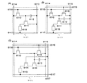
本発明の表示装置に具備される保護回路の一例について説明する。保護回路は、TFT、ダイオード、抵抗素子及び容量素子等から選択された1つ又は複数の素子によって構成されるものであり、以下にはいくつかの保護回路の構成とその動作について説明する。まず、外部回路と内部回路の間に配置される保護回路であって、1つの入力端子に対応した保護回路の等価回路図の構成について、図17を用いて説明する。図17(A)に示す保護回路は、P型TFT7220、7230、容量素子7210、7240、抵抗素子7250を有する。抵抗素子7250は2端子の抵抗であり、一端には入力電圧Vin(以下、Vinと表記)が、他端には低電位電圧VSS(以下、VSSと表記)が与えられる。抵抗素子7250は、入力端子にVinが与えられなくなったときに、配線の電位をVSSにおとすために設けられており、その抵抗値は配線の配線抵抗よりも十分に大きく設定する。
An example of a protection circuit included in the display device of the present invention will be described. The protection circuit is composed of one or a plurality of elements selected from a TFT, a diode, a resistance element, a capacitance element, and the like, and the configurations and operations of some protection circuits will be described below. First, a configuration of an equivalent circuit diagram of a protection circuit arranged between an external circuit and an internal circuit and corresponding to one input terminal will be described with reference to FIG. The protection circuit illustrated in FIG. 17A includes P-
Vinが高電位電圧VDD(以下、VDDと称する)よりも高い場合、そのゲート・ソース間電圧の関係から、TFT7220はオン、TFT7230はオフとなる。そうすると、VDDがTFT7220を介して、配線に与えられる。従って、雑音等により、VinがVDDよりも高くなっても、配線に与えられる電圧は、VDDよりも高くなることはない。一方、VinがVSSよりも低い場合、そのゲート・ソース間電圧の関係から、TFT7220はオフ、TFT7230はオンとなる。そうすると、VSSが配線に与えられる。従って、雑音等により、VinがVSSよりも低くなっても、配線に与えられる電圧は、VDDよりも高くなることはない。さらに、容量素子7210、7240により、入力端子からの電圧にパルス状の雑音を鈍らせることができ、雑音による電圧の急峻な変化をある程度小さくすることができる。
When Vin is higher than a high potential voltage VDD (hereinafter referred to as VDD), the
上記構成の保護回路の配置により、配線の電圧は、VSSからVDD間の範囲に保たれ、この範囲外の異常に高いまたは低い電圧の印加から保護される。さらに、信号が入力される入力端子に保護回路を設けることで、信号が入力されていないときに、信号が与えられる全ての配線の電圧を、一定(ここではVSS)の高さに保つことができる。つまり信号が入力されていないときは、配線同士をショートした状態にすることができるショートリングとしての機能も有する。そのため、配線間での電圧差に起因する静電破壊を防ぐことができる。また、信号を入力しているときは、抵抗素子7250の抵抗値が十分に大きいので、配線に与えられる信号がVSSに引っ張られることがない。
With the arrangement of the protection circuit having the above configuration, the voltage of the wiring is kept in a range between VSS and VDD, and is protected from application of an abnormally high or low voltage outside this range. Further, by providing a protection circuit at an input terminal to which a signal is input, the voltage of all wirings to which a signal is applied can be kept constant (here, VSS) when no signal is input. it can. In other words, when a signal is not input, it also has a function as a short ring that can make the wirings short-circuited. For this reason, electrostatic breakdown due to a voltage difference between the wirings can be prevented. Further, when a signal is input, the resistance value of the
図17(B)に示す保護回路は、P型TFT7220、7230を、整流性を有するダイオード7260、7270で代用した等価回路図である。図17(C)に示す保護回路は、P型TFT7220、7230を、TFT7350、7360、7370、7380で代用した等価回路図である。また、上記とは別の構成の保護回路として、図17(D)に示す保護回路は、抵抗素子7280、7290と、TFT7300を有する。図17(E)に示す保護回路は、抵抗素子7280、7290、P型TFT7310及びN型TFT7320を有する。図17(D)(E)の両構成とも、端子7330には配線などが接続され、この配線などの電位が急激に変化した場合に、N型TFT7300、又はP型TFT7310及びN型TFT7320がオンすることで、電流を端子7330から端子7340の方向に流す。そうすると、端子7330に接続された電位の急激な変動を緩和し、素子の損傷又は破壊を防止することができる。なお、上記保護回路を構成する素子は、耐圧に優れた非晶質半導体により構成することが好ましい。本実施例は、上記の実施の形態と自由に組み合わせることが可能である。
The protection circuit shown in FIG. 17B is an equivalent circuit diagram in which P-
本発明を適用して作製される電子機器の一例として、デジタルカメラ、カーオーディオなどの音響再生装置、ノート型パーソナルコンピュータ、ゲーム機器、携帯情報端末(携帯電話、携帯型ゲーム機等)、家庭用ゲーム機などの記録媒体を備えた画像再生装置などが挙げられる。それら電子機器の具体例を図18、19に示す。 As an example of an electronic device manufactured by applying the present invention, a digital camera, a sound reproducing device such as a car audio, a notebook personal computer, a game device, a portable information terminal (mobile phone, portable game machine, etc.), home use An image reproducing device including a recording medium such as a game machine may be used. Specific examples of these electronic devices are shown in FIGS.
図18(A)はテレビ受像機(テレビ、テレビジョン装置、テレビジョン受像機とも呼ぶ)であり、筐体9501、表示部9502等を含む。図18(B)はパソコン用のモニタであり、筐体9601、表示部9602等を含む。図18(C)はノート型パーソナルコンピュータであり、筐体9801、表示部9802等を含む。本発明は、上記電子機器の表示部の作製に適用される。上記の電子機器の表示部は、携帯端末と比較すると大型であるため、必然的に、第4世代、第5世代以降の大型のガラス基板を用いることになる。従って、材料の利用効率が高く、またフォトリソグラフィ工程を用いる場合と比較して工程数を削減することが可能な液滴吐出法用いる本発明を適用すれば、低価格化が実現される。また、作製工程や費用の面から、非晶質半導体や微結晶半導体をチャネル部としたトランジスタにより構成することが好ましい。
FIG. 18A illustrates a television receiver (also referred to as a television, a television device, or a television receiver), which includes a
図19(A)は携帯端末のうちの携帯電話であり、筐体9101、表示部9102等を含む。図19(B)は携帯端末のうちのPDA(personal digital assistant)であり、筐体9201、表示部9202等を含む。図19(C)はビデオカメラであり、表示部9701、9702等を含む。本発明は、上記電子機器の表示部の作製に適用される。上記電子機器は、携帯端末であるため、その画面が比較的小型である。従って、表示部と同一の基板上に、多結晶半導体をチャネルとした薄膜トランジスタを用いた駆動回路やCPU(Central Processing Unit、中央処理ユニット)等の機能回路、多層配線を搭載して、小型化を図ることが好ましい。この際、工程数を削減することができる液滴吐出法で配線を形成する本発明を用いると、低価格化が実現される。さらに、上記電子機器は携帯端末であるため、薄型、軽量、小型の点で付加価値を図るために、発光素子を用いた表示部とするとよい。本実施例は、上記の実施の形態、実施例と自由に組み合わせることができる。
FIG. 19A illustrates a mobile phone among mobile terminals, which includes a
50・・・基板、51・・・導電層、52・・・絶縁層
53・・・液滴吐出手段、54・・・導電層、55・・・導電層
56・・・フォトマスク、57・・・絶縁層、58・・・導電層
50 ... Substrate, 51 ... Conductive layer, 52 ... Insulating
Claims (19)
前記第1の導電層に接する第1のマスクを液滴吐出法により形成し、
前記第1のマスクを用いて、前記第1の導電層をエッチングして、ゲート電極としての機能を有する第2の導電層を形成し、
前記第1のマスク上に、ゲート絶縁膜としての機能を有する絶縁層と、第1の半導体層及び一導電型が付与された第2の半導体層を積層形成し、
前記第2の半導体層に接する第2のマスクを液滴吐出法により形成し、
前記第2のマスクを用いて、前記第1の半導体層及び前記第2の半導体層を同時にエッチングして、活性層としての機能を有する第3の半導体層及び一導電型が付与された第4の半導体層を形成し、
前記第4の半導体層に接する第3の導電層を形成し、
前記第3の導電層に接する第3のマスクを液滴吐出法により形成し、
前記第3のマスクを用いて、前記第4の半導体層及び前記第3の導電層を同時にエッチングして、第5の半導体層及びソース・ドレイン配線としての機能を有する第4の導電層を形成し、
前記第1乃至前記第3のマスクのうち、少なくとも1つは除去しないことを特徴とする薄膜トランジスタの作製方法。 Forming a first conductive layer on the substrate;
Forming a first mask in contact with the first conductive layer by a droplet discharge method;
The first conductive layer is etched using the first mask to form a second conductive layer having a function as a gate electrode ,
On the first mask , an insulating layer having a function as a gate insulating film, a first semiconductor layer, and a second semiconductor layer imparted with one conductivity type are stacked.
Forming a second mask in contact with the second semiconductor layer by a droplet discharge method;
Using the second mask, the first semiconductor layer and the second semiconductor layer are simultaneously etched to provide a third semiconductor layer having a function as an active layer and a fourth conductivity type. Forming a semiconductor layer,
Forming a third conductive layer in contact with the fourth semiconductor layer;
Forming a third mask in contact with the third conductive layer by a droplet discharge method;
Using the third mask, the fourth semiconductor layer and the third conductive layer are simultaneously etched to form a fifth semiconductor layer and a fourth conductive layer functioning as a source / drain wiring. And
A method for manufacturing a thin film transistor, wherein at least one of the first to third masks is not removed.
前記第1の導電層に接する第1のマスクを液滴吐出法により形成し、
前記第1のマスクを用いて、前記第1の導電層をエッチングして、ゲート電極としての機能を有する第2の導電層を形成し、
前記第1のマスク上に、ゲート絶縁膜としての機能を有する第1の絶縁層と、第1の半導体層と、第2の絶縁層とを積層形成し、
前記第2の絶縁層に接する第2のマスクを液滴吐出法により形成し、
前記第2のマスクを用いて、前記第2の絶縁層をエッチングして、チャネル保護層としての機能を有する第3の絶縁層を形成し、
前記第2のマスク上に、一導電型が付与された第2の半導体層を形成し、
前記第2の半導体層に接する第3のマスクを液滴吐出法により形成し、
前記第3のマスクを用いて、前記第1の半導体層及び前記第2の半導体層を同時にエッチングして、活性層としての機能を有する第3の半導体層及び一導電型が付与された第4の半導体層を形成し、
前記第4の半導体層と接する第3の導電層を形成し、
前記第3の導電層に接する第4のマスクを液滴吐出法により形成し、
前記第4のマスクを用いて、前記第4の半導体層及び前記第3の導電層を同時にエッチングして、第5の半導体層及びソース・ドレイン配線としての機能を有する第4の導電層を形成し、
前記第1乃至前記第4のマスクのうち、少なくとも1つは除去しないことを特徴とする薄膜トランジスタの作製方法。 Forming a first conductive layer on the substrate;
Forming a first mask in contact with the first conductive layer by a droplet discharge method;
The first conductive layer is etched using the first mask to form a second conductive layer having a function as a gate electrode ,
A first insulating layer having a function as a gate insulating film, a first semiconductor layer, and a second insulating layer are stacked over the first mask;
Forming a second mask in contact with the second insulating layer by a droplet discharge method;
The second insulating layer is etched using the second mask to form a third insulating layer having a function as a channel protective layer ,
Forming a second semiconductor layer imparted with one conductivity type on the second mask;
Forming a third mask in contact with the second semiconductor layer by a droplet discharge method;
Using the third mask, the first semiconductor layer and the second semiconductor layer are simultaneously etched to provide a third semiconductor layer having a function as an active layer and a fourth conductivity type. Forming a semiconductor layer,
Forming a third conductive layer in contact with the fourth semiconductor layer;
Forming a fourth mask in contact with the third conductive layer by a droplet discharge method;
Using the fourth mask, the fourth semiconductor layer and the third conductive layer are simultaneously etched to form a fifth semiconductor layer and a fourth conductive layer functioning as a source / drain wiring. And
A method for manufacturing a thin film transistor, wherein at least one of the first to fourth masks is not removed.
前記第1の半導体層に接する、ゲート絶縁膜としての機能を有する第1のマスクを液滴吐出法により形成し、
前記第1のマスクを用いて、前記第1の半導体層をエッチングして、活性層としての機能を有する第2の半導体層を形成し、
前記第1のマスク上に、第1の導電層を形成し、
前記第1の導電層に接する第2のマスクを液滴吐出法により形成し、
前記第2のマスクを用いて、前記第1の導電層をエッチングして、ゲート電極としての機能を有する第2の導電層を形成し、
前記第1のマスクと前記第2のマスクのうち、少なくとも1つは除去しないことを特徴とする薄膜トランジスタの作製方法。 Forming a first semiconductor layer on a substrate;
Forming a first mask in contact with the first semiconductor layer and having a function as a gate insulating film by a droplet discharge method;
Etching the first semiconductor layer using the first mask to form a second semiconductor layer having a function as an active layer ;
Forming a first conductive layer on the first mask;
Forming a second mask in contact with the first conductive layer by a droplet discharge method;
Etching the first conductive layer using the second mask to form a second conductive layer having a function as a gate electrode ;
A method for manufacturing a thin film transistor, wherein at least one of the first mask and the second mask is not removed.
前記第1の半導体層に接する第1のマスクを液滴吐出法により形成し、
前記第1のマスクを用いて、前記第1の半導体層をエッチングして、一導電型が付与された第2の半導体層を形成し、
前記第2の半導体層に接する第3の半導体層を形成し、
前記第3の半導体層に接する第2のマスクを液滴吐出法により形成し、
前記第2のマスクを用いて、前記第2の半導体層及び前記第3の半導体層をエッチングして、一導電型が付与された第4の半導体層と、活性層としての機能を有する第5の半導体層を形成し、
前記第2のマスク上に、ゲート絶縁膜としての機能を有する絶縁層と、第2の導電層を積層形成し、
前記第2の導電層に接する第3のマスクを液滴吐出法により形成し、
前記第3のマスクを用いて、前記第2の導電層をエッチングして、ゲート電極としての機能を有する第3の導電層を形成し、
前記第1乃至前記第3のマスクのうち、少なくとも1つは除去しないことを特徴とする薄膜トランジスタの作製方法。 A first conductive layer having a function as a source / drain wiring and a first semiconductor layer imparted with one conductivity type are stacked on the substrate,
Forming a first mask in contact with the first semiconductor layer by a droplet discharge method;
The first semiconductor layer is etched using the first mask to form a second semiconductor layer imparted with one conductivity type,
Forming a third semiconductor layer in contact with the second semiconductor layer;
Forming a second mask in contact with the third semiconductor layer by a droplet discharge method;
The second semiconductor layer and the third semiconductor layer are etched using the second mask, and a fourth semiconductor layer imparted with one conductivity type and a fifth semiconductor layer functioning as an active layer Forming a semiconductor layer,
An insulating layer having a function as a gate insulating film and a second conductive layer are stacked over the second mask;
Forming a third mask in contact with the second conductive layer by a droplet discharge method;
Etching the second conductive layer using the third mask to form a third conductive layer having a function as a gate electrode ;
A method for manufacturing a thin film transistor, wherein at least one of the first to third masks is not removed.
前記第1の半導体層に接する第1のマスクを液滴吐出法により形成し、
前記第1のマスクを用いて、前記第1の半導体層をエッチングして、活性層としての機能を有する第2の半導体層を形成し、
前記第2の半導体層上に、一導電型が付与された第3の半導体層と、第1の導電層を積層形成し、
前記第1の導電層に接する第2のマスクを液滴吐出法により形成し、
前記第2のマスクを用いて、前記第3の半導体層及び前記第1の導電層をエッチングして、一導電型が付与された第4の半導体層と、ソース・ドレイン配線としての機能を有する第2の導電層を形成し、
前記第2のマスク上に、ゲート絶縁膜としての機能を有する絶縁層と、第3の導電層を積層形成し、
前記第3の導電層に接する第3のマスクを液滴吐出法により形成し、
前記第3のマスクを用いて、前記第3の導電層をエッチングして、ゲート電極としての機能を有する第4の導電層を形成し、
前記第1乃至前記第3のマスクのうち、少なくとも1つは除去しないことを特徴とする薄膜トランジスタの作製方法。 Forming a first semiconductor layer on a substrate;
Forming a first mask in contact with the first semiconductor layer by a droplet discharge method;
Etching the first semiconductor layer using the first mask to form a second semiconductor layer having a function as an active layer ;
On the second semiconductor layer, a third semiconductor layer imparted with one conductivity type and a first conductive layer are stacked.
Forming a second mask in contact with the first conductive layer by a droplet discharge method;
Using the second mask, the third semiconductor layer and the first conductive layer are etched to have a function of a fourth semiconductor layer imparted with one conductivity type and a source / drain wiring. Forming a second conductive layer;
An insulating layer having a function as a gate insulating film and a third conductive layer are stacked over the second mask;
Forming a third mask in contact with the third conductive layer by a droplet discharge method;
The third conductive layer is etched using the third mask to form a fourth conductive layer having a function as a gate electrode ,
A method for manufacturing a thin film transistor, wherein at least one of the first to third masks is not removed.
前記第1の導電層と前記第3の導電層は、液滴吐出法、スパッタリング法又は蒸着法により形成することを特徴とする薄膜トランジスタの作製方法。 In claim 1 or claim 2,
The method for manufacturing a thin film transistor, wherein the first conductive layer and the third conductive layer are formed by a droplet discharge method, a sputtering method, or an evaporation method.
前記第1の導電層と前記第3の導電層は、銀、金、銅又はインジウム錫酸化物により形成することを特徴とする薄膜トランジスタの作製方法。 In claim 1 or claim 2,
The first conductive layer and the third conductive layer are formed using silver, gold, copper, or indium tin oxide.
前記第1の導電層は、液滴吐出法、スパッタリング法又は蒸着法により形成することを特徴とする薄膜トランジスタの作製方法。 In claim 3,
The method for manufacturing a thin film transistor, wherein the first conductive layer is formed by a droplet discharge method, a sputtering method, or an evaporation method.
前記第1の導電層は、銀、金、銅又はインジウム錫酸化物により形成することを特徴とする薄膜トランジスタの作製方法。 In claim 3,
The method for manufacturing a thin film transistor, wherein the first conductive layer is formed using silver, gold, copper, or indium tin oxide.
前記第1の導電層と前記第2の導電層は、液滴吐出法、スパッタリング法又は蒸着法により形成することを特徴とする薄膜トランジスタの作製方法。 Oite to claim 4,
The method for manufacturing a thin film transistor, wherein the first conductive layer and the second conductive layer are formed by a droplet discharge method, a sputtering method, or an evaporation method.
前記第1の導電層と前記第2の導電層は、銀、金、銅又はインジウム錫酸化物により形成することを特徴とする薄膜トランジスタの作製方法。 Oite to claim 4,
The first conductive layer and the second conductive layer are formed using silver, gold, copper, or indium tin oxide.
前記第1の導電層と前記第3の導電層は、液滴吐出法、スパッタリング法又は蒸着法により形成することを特徴とする薄膜トランジスタの作製方法。The method for manufacturing a thin film transistor, wherein the first conductive layer and the third conductive layer are formed by a droplet discharge method, a sputtering method, or an evaporation method.
前記第1の導電層と前記第3の導電層は、銀、金、銅又はインジウム錫酸化物により形成することを特徴とする薄膜トランジスタの作製方法。The first conductive layer and the third conductive layer are formed using silver, gold, copper, or indium tin oxide.
前記第1乃至前記第3のマスクは、液滴吐出法により形成された絶縁層に、フォトマスクを用いた露光処理及び現像処理を行って形成することを特徴とする薄膜トランジスタの作製方法。 In any one of Claim 1, Claim 4, or Claim 5,
The first to third masks are formed by performing exposure treatment and development treatment using a photomask on an insulating layer formed by a droplet discharge method.
前記第1乃至前記第3のマスクは、有機材料又は珪素と酸素との結合で骨格構造が形成された材料で形成することを特徴とする薄膜トランジスタの作製方法。 In any one of Claim 1, Claim 4, or Claim 5,
The method for manufacturing a thin film transistor, wherein the first to third masks are formed using an organic material or a material in which a skeleton structure is formed by a bond of silicon and oxygen.
前記第1乃至前記第4のマスクは、液滴吐出法により形成された絶縁層に、フォトマスクを用いた露光処理及び現像処理を行って形成することを特徴とする薄膜トランジスタの作製方法。 In claim 2,
The first to fourth masks are formed by performing exposure treatment and development treatment using a photomask on an insulating layer formed by a droplet discharge method.
前記第1乃至前記第4のマスクは、有機材料又は珪素と酸素との結合で骨格構造が形成された材料で形成することを特徴とする薄膜トランジスタの作製方法。 In claim 2,
The method for manufacturing a thin film transistor, wherein the first to fourth masks are formed using an organic material or a material in which a skeleton structure is formed by a bond of silicon and oxygen.
前記第1のマスク及び前記第2のマスクは、液滴吐出法により形成された絶縁層に、フォトマスクを用いた露光処理及び現像処理を行って形成することを特徴とする薄膜トランジスタの作製方法。 In claim 3,
The method for manufacturing a thin film transistor, wherein the first mask and the second mask are formed by performing exposure treatment and development treatment using a photomask on an insulating layer formed by a droplet discharge method.
前記第1のマスク及び前記第2のマスクは、有機材料又は珪素と酸素との結合で骨格構造が形成された材料で形成することを特徴とする薄膜トランジスタの作製方法。 In claim 3,
The method for manufacturing a thin film transistor, wherein the first mask and the second mask are formed using an organic material or a material in which a skeleton structure is formed by a bond of silicon and oxygen.
Priority Applications (1)
| Application Number | Priority Date | Filing Date | Title |
|---|---|---|---|
| JP2004297094A JP4718818B2 (en) | 2003-10-10 | 2004-10-12 | Method for manufacturing thin film transistor |
Applications Claiming Priority (3)
| Application Number | Priority Date | Filing Date | Title |
|---|---|---|---|
| JP2003351974 | 2003-10-10 | ||
| JP2003351974 | 2003-10-10 | ||
| JP2004297094A JP4718818B2 (en) | 2003-10-10 | 2004-10-12 | Method for manufacturing thin film transistor |
Publications (3)
| Publication Number | Publication Date |
|---|---|
| JP2005136403A JP2005136403A (en) | 2005-05-26 |
| JP2005136403A5 JP2005136403A5 (en) | 2007-08-30 |
| JP4718818B2 true JP4718818B2 (en) | 2011-07-06 |
Family
ID=34656092
Family Applications (1)
| Application Number | Title | Priority Date | Filing Date |
|---|---|---|---|
| JP2004297094A Expired - Fee Related JP4718818B2 (en) | 2003-10-10 | 2004-10-12 | Method for manufacturing thin film transistor |
Country Status (1)
| Country | Link |
|---|---|
| JP (1) | JP4718818B2 (en) |
Families Citing this family (3)
| Publication number | Priority date | Publication date | Assignee | Title |
|---|---|---|---|---|
| JP2008226993A (en) * | 2007-03-09 | 2008-09-25 | Advanced Lcd Technologies Development Center Co Ltd | Semiconductor device and its manufacturing method |
| KR20220136513A (en) | 2009-12-04 | 2022-10-07 | 가부시키가이샤 한도오따이 에네루기 켄큐쇼 | Semiconductor device |
| JP2012164876A (en) * | 2011-02-08 | 2012-08-30 | Mitsubishi Chemicals Corp | Method of forming interconnection or electrode, electronic device, and method of manufacturing the same |
Citations (1)
| Publication number | Priority date | Publication date | Assignee | Title |
|---|---|---|---|---|
| JP2003179234A (en) * | 2001-09-05 | 2003-06-27 | Konica Corp | Organic semiconductor element and manufacturing method thereof |
Family Cites Families (3)
| Publication number | Priority date | Publication date | Assignee | Title |
|---|---|---|---|---|
| JPS62140466A (en) * | 1985-12-16 | 1987-06-24 | Matsushita Electric Ind Co Ltd | Manufacture of thin-film transistor circuit |
| JPS62263676A (en) * | 1986-05-09 | 1987-11-16 | Seiko Instr & Electronics Ltd | Manufacture of thin film transistor |
| JPH11340129A (en) * | 1998-05-28 | 1999-12-10 | Seiko Epson Corp | Method and device for manufacturing pattern |
-
2004
- 2004-10-12 JP JP2004297094A patent/JP4718818B2/en not_active Expired - Fee Related
Patent Citations (1)
| Publication number | Priority date | Publication date | Assignee | Title |
|---|---|---|---|---|
| JP2003179234A (en) * | 2001-09-05 | 2003-06-27 | Konica Corp | Organic semiconductor element and manufacturing method thereof |
Also Published As
| Publication number | Publication date |
|---|---|
| JP2005136403A (en) | 2005-05-26 |
Similar Documents
| Publication | Publication Date | Title |
|---|---|---|
| KR101030698B1 (en) | Method for manufacturing semiconductor device | |
| US7365805B2 (en) | Display device, manufacturing method thereof, and television receiver | |
| US7247529B2 (en) | Method for manufacturing display device | |
| US9237657B2 (en) | Wiring substrate, semiconductor device, and method for manufacturing thereof | |
| US7955907B2 (en) | Semiconductor device, television set, and method for manufacturing the same | |
| JP4731970B2 (en) | Light emitting device and manufacturing method thereof | |
| US7795730B2 (en) | Wiring substrate and method of manufacturing thereof, and thin film transistor and method of manufacturing thereof | |
| JP4498715B2 (en) | Method for manufacturing semiconductor device | |
| JP4554292B2 (en) | Method for manufacturing thin film transistor | |
| JP4737971B2 (en) | Liquid crystal display device and method for manufacturing liquid crystal display device | |
| JP4884675B2 (en) | Method for manufacturing semiconductor device | |
| JP4877866B2 (en) | Method for manufacturing semiconductor device | |
| JP4718818B2 (en) | Method for manufacturing thin film transistor | |
| JP4877868B2 (en) | Method for manufacturing display device | |
| JP4741218B2 (en) | Liquid crystal display device, manufacturing method thereof, and liquid crystal television receiver | |
| JP4817627B2 (en) | Method for manufacturing display device | |
| JP4597627B2 (en) | Wiring board manufacturing method | |
| JP4712332B2 (en) | Method for manufacturing thin film transistor | |
| JP4916653B2 (en) | Wiring substrate manufacturing method and semiconductor device manufacturing method | |
| JP4683898B2 (en) | Method for manufacturing semiconductor device | |
| JP4624078B2 (en) | Method for manufacturing liquid crystal display device |
Legal Events
| Date | Code | Title | Description |
|---|---|---|---|
| A521 | Written amendment |
Free format text: JAPANESE INTERMEDIATE CODE: A523 Effective date: 20070712 |
|
| A621 | Written request for application examination |
Free format text: JAPANESE INTERMEDIATE CODE: A621 Effective date: 20070712 |
|
| A977 | Report on retrieval |
Free format text: JAPANESE INTERMEDIATE CODE: A971007 Effective date: 20101022 |
|
| A131 | Notification of reasons for refusal |
Free format text: JAPANESE INTERMEDIATE CODE: A131 Effective date: 20110222 |
|
| A521 | Written amendment |
Free format text: JAPANESE INTERMEDIATE CODE: A523 Effective date: 20110308 |
|
| TRDD | Decision of grant or rejection written | ||
| A01 | Written decision to grant a patent or to grant a registration (utility model) |
Free format text: JAPANESE INTERMEDIATE CODE: A01 Effective date: 20110329 |
|
| A01 | Written decision to grant a patent or to grant a registration (utility model) |
Free format text: JAPANESE INTERMEDIATE CODE: A01 |
|
| A61 | First payment of annual fees (during grant procedure) |
Free format text: JAPANESE INTERMEDIATE CODE: A61 Effective date: 20110401 |
|
| R150 | Certificate of patent or registration of utility model |
Free format text: JAPANESE INTERMEDIATE CODE: R150 |
|
| FPAY | Renewal fee payment (event date is renewal date of database) |
Free format text: PAYMENT UNTIL: 20140408 Year of fee payment: 3 |
|
| FPAY | Renewal fee payment (event date is renewal date of database) |
Free format text: PAYMENT UNTIL: 20140408 Year of fee payment: 3 |
|
| R250 | Receipt of annual fees |
Free format text: JAPANESE INTERMEDIATE CODE: R250 |
|
| R250 | Receipt of annual fees |
Free format text: JAPANESE INTERMEDIATE CODE: R250 |
|
| R250 | Receipt of annual fees |
Free format text: JAPANESE INTERMEDIATE CODE: R250 |
|
| LAPS | Cancellation because of no payment of annual fees |