JP4339000B2 - Semiconductor device and manufacturing method thereof - Google Patents
Semiconductor device and manufacturing method thereof Download PDFInfo
- Publication number
- JP4339000B2 JP4339000B2 JP2003084808A JP2003084808A JP4339000B2 JP 4339000 B2 JP4339000 B2 JP 4339000B2 JP 2003084808 A JP2003084808 A JP 2003084808A JP 2003084808 A JP2003084808 A JP 2003084808A JP 4339000 B2 JP4339000 B2 JP 4339000B2
- Authority
- JP
- Japan
- Prior art keywords
- insulating film
- wiring
- layer
- semiconductor device
- substrate
- Prior art date
- Legal status (The legal status is an assumption and is not a legal conclusion. Google has not performed a legal analysis and makes no representation as to the accuracy of the status listed.)
- Expired - Fee Related
Links
- 239000004065 semiconductor Substances 0.000 title claims description 61
- 238000004519 manufacturing process Methods 0.000 title claims description 18
- 239000010408 film Substances 0.000 claims description 162
- 239000000758 substrate Substances 0.000 claims description 52
- 238000000034 method Methods 0.000 claims description 46
- 150000002894 organic compounds Chemical class 0.000 claims description 38
- 239000010949 copper Substances 0.000 claims description 25
- 239000010409 thin film Substances 0.000 claims description 25
- 229910052802 copper Inorganic materials 0.000 claims description 24
- 238000005530 etching Methods 0.000 claims description 24
- RYGMFSIKBFXOCR-UHFFFAOYSA-N Copper Chemical compound [Cu] RYGMFSIKBFXOCR-UHFFFAOYSA-N 0.000 claims description 23
- 230000004888 barrier function Effects 0.000 claims description 23
- 239000004973 liquid crystal related substance Substances 0.000 claims description 23
- 239000000463 material Substances 0.000 claims description 22
- PXHVJJICTQNCMI-UHFFFAOYSA-N Nickel Chemical compound [Ni] PXHVJJICTQNCMI-UHFFFAOYSA-N 0.000 claims description 19
- 239000000956 alloy Substances 0.000 claims description 19
- 229910045601 alloy Inorganic materials 0.000 claims description 18
- BASFCYQUMIYNBI-UHFFFAOYSA-N platinum Chemical compound [Pt] BASFCYQUMIYNBI-UHFFFAOYSA-N 0.000 claims description 15
- XEEYBQQBJWHFJM-UHFFFAOYSA-N Iron Chemical compound [Fe] XEEYBQQBJWHFJM-UHFFFAOYSA-N 0.000 claims description 14
- 238000007789 sealing Methods 0.000 claims description 14
- 238000006243 chemical reaction Methods 0.000 claims description 12
- PCHJSUWPFVWCPO-UHFFFAOYSA-N gold Chemical compound [Au] PCHJSUWPFVWCPO-UHFFFAOYSA-N 0.000 claims description 12
- 229910052737 gold Inorganic materials 0.000 claims description 12
- 239000010931 gold Substances 0.000 claims description 12
- 229910052709 silver Inorganic materials 0.000 claims description 12
- BQCADISMDOOEFD-UHFFFAOYSA-N Silver Chemical compound [Ag] BQCADISMDOOEFD-UHFFFAOYSA-N 0.000 claims description 11
- 229910052759 nickel Inorganic materials 0.000 claims description 11
- 230000008569 process Effects 0.000 claims description 11
- 239000004332 silver Substances 0.000 claims description 11
- 229910052804 chromium Inorganic materials 0.000 claims description 10
- 239000011651 chromium Substances 0.000 claims description 10
- VYZAMTAEIAYCRO-UHFFFAOYSA-N Chromium Chemical compound [Cr] VYZAMTAEIAYCRO-UHFFFAOYSA-N 0.000 claims description 8
- 229910052697 platinum Inorganic materials 0.000 claims description 8
- 229910052742 iron Inorganic materials 0.000 claims description 7
- 238000007747 plating Methods 0.000 claims description 7
- 229910052782 aluminium Inorganic materials 0.000 claims description 6
- XAGFODPZIPBFFR-UHFFFAOYSA-N aluminium Chemical compound [Al] XAGFODPZIPBFFR-UHFFFAOYSA-N 0.000 claims description 5
- 239000010410 layer Substances 0.000 description 137
- 239000011159 matrix material Substances 0.000 description 25
- XUIMIQQOPSSXEZ-UHFFFAOYSA-N Silicon Chemical compound [Si] XUIMIQQOPSSXEZ-UHFFFAOYSA-N 0.000 description 17
- 229910052710 silicon Inorganic materials 0.000 description 17
- 239000010703 silicon Substances 0.000 description 17
- 229910052751 metal Inorganic materials 0.000 description 15
- 239000002184 metal Substances 0.000 description 15
- 239000012535 impurity Substances 0.000 description 14
- 238000009713 electroplating Methods 0.000 description 10
- 229910052760 oxygen Inorganic materials 0.000 description 8
- VYPSYNLAJGMNEJ-UHFFFAOYSA-N Silicium dioxide Chemical compound O=[Si]=O VYPSYNLAJGMNEJ-UHFFFAOYSA-N 0.000 description 7
- 229910052814 silicon oxide Inorganic materials 0.000 description 7
- 238000010438 heat treatment Methods 0.000 description 6
- 238000002347 injection Methods 0.000 description 6
- 239000007924 injection Substances 0.000 description 6
- 229920003227 poly(N-vinyl carbazole) Polymers 0.000 description 6
- 229910052581 Si3N4 Inorganic materials 0.000 description 5
- QVGXLLKOCUKJST-UHFFFAOYSA-N atomic oxygen Chemical compound [O] QVGXLLKOCUKJST-UHFFFAOYSA-N 0.000 description 5
- 229910052757 nitrogen Inorganic materials 0.000 description 5
- 239000001301 oxygen Substances 0.000 description 5
- 238000005268 plasma chemical vapour deposition Methods 0.000 description 5
- 239000000565 sealant Substances 0.000 description 5
- HQVNEWCFYHHQES-UHFFFAOYSA-N silicon nitride Chemical compound N12[Si]34N5[Si]62N3[Si]51N64 HQVNEWCFYHHQES-UHFFFAOYSA-N 0.000 description 5
- 239000000126 substance Substances 0.000 description 5
- IJGRMHOSHXDMSA-UHFFFAOYSA-N Atomic nitrogen Chemical compound N#N IJGRMHOSHXDMSA-UHFFFAOYSA-N 0.000 description 4
- 229920001609 Poly(3,4-ethylenedioxythiophene) Polymers 0.000 description 4
- 230000015572 biosynthetic process Effects 0.000 description 4
- 239000003795 chemical substances by application Substances 0.000 description 4
- 238000002425 crystallisation Methods 0.000 description 4
- 238000009792 diffusion process Methods 0.000 description 4
- 230000005281 excited state Effects 0.000 description 4
- 230000005525 hole transport Effects 0.000 description 4
- 239000012212 insulator Substances 0.000 description 4
- 239000011133 lead Substances 0.000 description 4
- 229910052718 tin Inorganic materials 0.000 description 4
- 239000011135 tin Substances 0.000 description 4
- XLOMVQKBTHCTTD-UHFFFAOYSA-N zinc oxide Inorganic materials [Zn]=O XLOMVQKBTHCTTD-UHFFFAOYSA-N 0.000 description 4
- ATJFFYVFTNAWJD-UHFFFAOYSA-N Tin Chemical compound [Sn] ATJFFYVFTNAWJD-UHFFFAOYSA-N 0.000 description 3
- 229910052785 arsenic Inorganic materials 0.000 description 3
- 239000000975 dye Substances 0.000 description 3
- 230000005283 ground state Effects 0.000 description 3
- 229910052739 hydrogen Inorganic materials 0.000 description 3
- 239000011229 interlayer Substances 0.000 description 3
- 238000004020 luminiscence type Methods 0.000 description 3
- 239000000203 mixture Substances 0.000 description 3
- 230000003287 optical effect Effects 0.000 description 3
- 230000010355 oscillation Effects 0.000 description 3
- 230000003647 oxidation Effects 0.000 description 3
- 238000007254 oxidation reaction Methods 0.000 description 3
- 238000005192 partition Methods 0.000 description 3
- 229910052698 phosphorus Inorganic materials 0.000 description 3
- 238000005498 polishing Methods 0.000 description 3
- 239000003566 sealing material Substances 0.000 description 3
- 239000002356 single layer Substances 0.000 description 3
- 150000005072 1,3,4-oxadiazoles Chemical class 0.000 description 2
- YLYPIBBGWLKELC-RMKNXTFCSA-N 2-[2-[(e)-2-[4-(dimethylamino)phenyl]ethenyl]-6-methylpyran-4-ylidene]propanedinitrile Chemical compound C1=CC(N(C)C)=CC=C1\C=C\C1=CC(=C(C#N)C#N)C=C(C)O1 YLYPIBBGWLKELC-RMKNXTFCSA-N 0.000 description 2
- KRHYYFGTRYWZRS-UHFFFAOYSA-N Fluorane Chemical compound F KRHYYFGTRYWZRS-UHFFFAOYSA-N 0.000 description 2
- KDLHZDBZIXYQEI-UHFFFAOYSA-N Palladium Chemical compound [Pd] KDLHZDBZIXYQEI-UHFFFAOYSA-N 0.000 description 2
- 229910008484 TiSi Inorganic materials 0.000 description 2
- 230000004913 activation Effects 0.000 description 2
- 239000007864 aqueous solution Substances 0.000 description 2
- 239000011248 coating agent Substances 0.000 description 2
- 238000000576 coating method Methods 0.000 description 2
- VBVAVBCYMYWNOU-UHFFFAOYSA-N coumarin 6 Chemical compound C1=CC=C2SC(C3=CC4=CC=C(C=C4OC3=O)N(CC)CC)=NC2=C1 VBVAVBCYMYWNOU-UHFFFAOYSA-N 0.000 description 2
- 230000008025 crystallization Effects 0.000 description 2
- 238000010586 diagram Methods 0.000 description 2
- 230000000694 effects Effects 0.000 description 2
- 230000005284 excitation Effects 0.000 description 2
- 239000011152 fibreglass Substances 0.000 description 2
- 239000007789 gas Substances 0.000 description 2
- 229910010272 inorganic material Inorganic materials 0.000 description 2
- 239000011147 inorganic material Substances 0.000 description 2
- 238000005499 laser crystallization Methods 0.000 description 2
- 239000007769 metal material Substances 0.000 description 2
- VOFUROIFQGPCGE-UHFFFAOYSA-N nile red Chemical compound C1=CC=C2C3=NC4=CC=C(N(CC)CC)C=C4OC3=CC(=O)C2=C1 VOFUROIFQGPCGE-UHFFFAOYSA-N 0.000 description 2
- 238000000059 patterning Methods 0.000 description 2
- 239000000049 pigment Substances 0.000 description 2
- 229920002620 polyvinyl fluoride Polymers 0.000 description 2
- 230000001681 protective effect Effects 0.000 description 2
- 239000012495 reaction gas Substances 0.000 description 2
- 239000002904 solvent Substances 0.000 description 2
- 238000004544 sputter deposition Methods 0.000 description 2
- 238000002834 transmittance Methods 0.000 description 2
- 229910052721 tungsten Inorganic materials 0.000 description 2
- 238000007740 vapor deposition Methods 0.000 description 2
- XLYOFNOQVPJJNP-UHFFFAOYSA-N water Substances O XLYOFNOQVPJJNP-UHFFFAOYSA-N 0.000 description 2
- OYQCBJZGELKKPM-UHFFFAOYSA-N zinc indium(3+) oxygen(2-) Chemical compound [O-2].[Zn+2].[O-2].[In+3] OYQCBJZGELKKPM-UHFFFAOYSA-N 0.000 description 2
- 239000011787 zinc oxide Substances 0.000 description 2
- KLCLIOISYBHYDZ-UHFFFAOYSA-N 1,4,4-triphenylbuta-1,3-dienylbenzene Chemical compound C=1C=CC=CC=1C(C=1C=CC=CC=1)=CC=C(C=1C=CC=CC=1)C1=CC=CC=C1 KLCLIOISYBHYDZ-UHFFFAOYSA-N 0.000 description 1
- 229910017073 AlLi Inorganic materials 0.000 description 1
- 229920002799 BoPET Polymers 0.000 description 1
- ZOXJGFHDIHLPTG-UHFFFAOYSA-N Boron Chemical compound [B] ZOXJGFHDIHLPTG-UHFFFAOYSA-N 0.000 description 1
- 229910004261 CaF 2 Inorganic materials 0.000 description 1
- -1 CaN Substances 0.000 description 1
- OKTJSMMVPCPJKN-UHFFFAOYSA-N Carbon Chemical compound [C] OKTJSMMVPCPJKN-UHFFFAOYSA-N 0.000 description 1
- 229940126062 Compound A Drugs 0.000 description 1
- NLDMNSXOCDLTTB-UHFFFAOYSA-N Heterophylliin A Natural products O1C2COC(=O)C3=CC(O)=C(O)C(O)=C3C3=C(O)C(O)=C(O)C=C3C(=O)OC2C(OC(=O)C=2C=C(O)C(O)=C(O)C=2)C(O)C1OC(=O)C1=CC(O)=C(O)C(O)=C1 NLDMNSXOCDLTTB-UHFFFAOYSA-N 0.000 description 1
- 229910017911 MgIn Inorganic materials 0.000 description 1
- 239000005041 Mylar™ Substances 0.000 description 1
- 229910000577 Silicon-germanium Inorganic materials 0.000 description 1
- 229910008812 WSi Inorganic materials 0.000 description 1
- LEVVHYCKPQWKOP-UHFFFAOYSA-N [Si].[Ge] Chemical compound [Si].[Ge] LEVVHYCKPQWKOP-UHFFFAOYSA-N 0.000 description 1
- AZWHFTKIBIQKCA-UHFFFAOYSA-N [Sn+2]=O.[O-2].[In+3] Chemical compound [Sn+2]=O.[O-2].[In+3] AZWHFTKIBIQKCA-UHFFFAOYSA-N 0.000 description 1
- NIXOWILDQLNWCW-UHFFFAOYSA-N acrylic acid group Chemical group C(C=C)(=O)O NIXOWILDQLNWCW-UHFFFAOYSA-N 0.000 description 1
- AZDRQVAHHNSJOQ-UHFFFAOYSA-N alumane Chemical group [AlH3] AZDRQVAHHNSJOQ-UHFFFAOYSA-N 0.000 description 1
- 239000012298 atmosphere Substances 0.000 description 1
- 230000005540 biological transmission Effects 0.000 description 1
- 229910052796 boron Inorganic materials 0.000 description 1
- 239000003990 capacitor Substances 0.000 description 1
- 229910052799 carbon Inorganic materials 0.000 description 1
- 239000003054 catalyst Substances 0.000 description 1
- 238000004140 cleaning Methods 0.000 description 1
- 238000010549 co-Evaporation Methods 0.000 description 1
- 150000001875 compounds Chemical class 0.000 description 1
- 230000007423 decrease Effects 0.000 description 1
- 239000002274 desiccant Substances 0.000 description 1
- 230000006866 deterioration Effects 0.000 description 1
- 238000011161 development Methods 0.000 description 1
- 230000005684 electric field Effects 0.000 description 1
- 239000003822 epoxy resin Substances 0.000 description 1
- 238000001704 evaporation Methods 0.000 description 1
- 230000001747 exhibiting effect Effects 0.000 description 1
- 238000005984 hydrogenation reaction Methods 0.000 description 1
- 229910052738 indium Inorganic materials 0.000 description 1
- AMGQUBHHOARCQH-UHFFFAOYSA-N indium;oxotin Chemical compound [In].[Sn]=O AMGQUBHHOARCQH-UHFFFAOYSA-N 0.000 description 1
- 239000011261 inert gas Substances 0.000 description 1
- 230000001678 irradiating effect Effects 0.000 description 1
- 238000004518 low pressure chemical vapour deposition Methods 0.000 description 1
- 238000012423 maintenance Methods 0.000 description 1
- 230000007257 malfunction Effects 0.000 description 1
- 230000007246 mechanism Effects 0.000 description 1
- 230000008018 melting Effects 0.000 description 1
- 238000002844 melting Methods 0.000 description 1
- 229910021645 metal ion Inorganic materials 0.000 description 1
- 238000002156 mixing Methods 0.000 description 1
- 229910052750 molybdenum Inorganic materials 0.000 description 1
- NMVZHJHQIMLNBM-UHFFFAOYSA-N n,n-dimethyl-4-[2-(6-methyl-4h-pyran-2-yl)ethenyl]aniline Chemical compound C1=CC(N(C)C)=CC=C1C=CC1=CCC=C(C)O1 NMVZHJHQIMLNBM-UHFFFAOYSA-N 0.000 description 1
- 239000011368 organic material Substances 0.000 description 1
- 239000003960 organic solvent Substances 0.000 description 1
- AHLBNYSZXLDEJQ-FWEHEUNISA-N orlistat Chemical compound CCCCCCCCCCC[C@H](OC(=O)[C@H](CC(C)C)NC=O)C[C@@H]1OC(=O)[C@H]1CCCCCC AHLBNYSZXLDEJQ-FWEHEUNISA-N 0.000 description 1
- 229910052763 palladium Inorganic materials 0.000 description 1
- 230000000737 periodic effect Effects 0.000 description 1
- 229920003023 plastic Polymers 0.000 description 1
- 239000004033 plastic Substances 0.000 description 1
- 229920000172 poly(styrenesulfonic acid) Polymers 0.000 description 1
- 229920000647 polyepoxide Polymers 0.000 description 1
- 229920000728 polyester Polymers 0.000 description 1
- 230000002265 prevention Effects 0.000 description 1
- 238000001552 radio frequency sputter deposition Methods 0.000 description 1
- 238000012827 research and development Methods 0.000 description 1
- 229920005989 resin Polymers 0.000 description 1
- 239000011347 resin Substances 0.000 description 1
- 230000004044 response Effects 0.000 description 1
- 229910052703 rhodium Inorganic materials 0.000 description 1
- 239000010948 rhodium Substances 0.000 description 1
- MHOVAHRLVXNVSD-UHFFFAOYSA-N rhodium atom Chemical compound [Rh] MHOVAHRLVXNVSD-UHFFFAOYSA-N 0.000 description 1
- 239000010944 silver (metal) Substances 0.000 description 1
- 239000000243 solution Substances 0.000 description 1
- 125000006850 spacer group Chemical group 0.000 description 1
- 238000003860 storage Methods 0.000 description 1
- 229910052715 tantalum Inorganic materials 0.000 description 1
- 229910052719 titanium Inorganic materials 0.000 description 1
- 229910052725 zinc Inorganic materials 0.000 description 1
- 239000011701 zinc Substances 0.000 description 1
Images


Description
【0001】
【発明の属する技術分野】
本発明は薄膜トランジスタ(以下、TFTという)で構成された回路を有する半導体装置およびその作製方法に関する。例えば、液晶表示装置に代表される電気光学装置やOLEDを有する発光装置を部品として搭載した電子機器に関する。
【0002】
なお、本明細書中において半導体装置とは、半導体特性を利用することで機能しうる装置全般を指し、電気光学装置、半導体回路および電子機器は全て半導体装置である。
【0003】
【従来の技術】
近年、絶縁表面を有する基板上に形成された半導体薄膜(厚さ数〜数百nm程度)を用いて薄膜トランジスタ(TFT)を構成する技術が注目されている。薄膜トランジスタはICや電気光学装置のような電子デバイスに広く応用され、特に画像表示装置のスイッチング素子として開発が急がれている。
【0004】
従来より、画像表示装置として液晶表示装置が知られている。パッシブ型の液晶表示装置に比べ高精細な画像が得られることからアクティブマトリクス型の液晶表示装置が多く用いられるようになっている。アクティブマトリクス型の液晶表示装置においては、マトリクス状に配置された画素電極を駆動することによって、画面上に表示パターンが形成される。詳しくは選択された画素電極と該画素電極に対応する対向電極との間に電圧が印加されることによって、画素電極と対向電極との間に配置された液晶層の光学変調が行われ、この光学変調が表示パターンとして観察者に認識される。
【0005】
また、OLEDを用いた発光装置にとって、TFTはアクティブマトリクス駆動方式を実現する上で、必須の素子となっている。従って、OLEDを用いた発光装置は、少なくとも、スイッチング素子として機能するTFTと、OLEDに電流を供給するTFTとが、各画素に設けられることになる。薄型軽量、高速応答性、直流低電圧駆動などの特徴を有する有機化合物を発光体として用いた発光素子は、次世代のフラットパネルディスプレイへの応用が期待されている。特に、発光素子をマトリクス状に配置した表示装置は、従来の液晶表示装置と比較して、視野角が広く視認性が優れる点に優位性があると考えられている。
【0006】
発光素子の発光機構は、一対の電極間に有機化合物層を挟んで電圧を印加することにより、陰極から注入された電子および陽極から注入された正孔が有機化合物層中の発光中心で再結合して分子励起子を形成し、その分子励起子が基底状態に戻る際にエネルギーを放出して発光するといわれている。励起状態には一重項励起と三重項励起が知られ、発光はどちらの励起状態を経ても可能であると考えられている。
【0007】
このような発光素子をマトリクス状に配置して形成された発光装置には、パッシブマトリクス駆動(単純マトリクス型)とアクティブマトリクス駆動(アクティブマトリクス型)といった駆動方法を用いることが可能である。しかし、画素密度が増えた場合には、画素(又は1ドット)毎にスイッチが設けられているアクティブマトリクス型の方が低電圧駆動できるので有利であると考えられている。
【0008】
このようなアクティブマトリクス型の表示装置(代表的には液晶表示装置および発光表示装置)の用途は広がっており、画面サイズの大面積化とともに高精細化や高開口率化や高信頼性の要求が高まっている。また、同時に生産性の向上や低コスト化の要求も高まっている。
【0009】
【発明が解決しようとする課題】
従来、上記TFTのゲート配線材料としてアルミニウムを用いてTFTを作製した場合、熱処理によってヒロックやウィスカー等の突起物の形成や、アルミニウム原子のチャネル形成領域への拡散により、TFTの動作不良やTFT特性の低下を引き起こしていた。そこで、熱処理に耐え得る金属材料、代表的には高い融点を有している金属元素を用いた場合、画面サイズが大面積化すると配線抵抗が高くなる等の問題が発生し、消費電力の増大等を引き起こしていた。
【0010】
そこで、本発明は、大画面化しても低消費電力を実現した半導体装置の構造およびその作製方法を提供することを課題としている。
【0011】
【課題を解決するための手段】
上記問題点を解決するため本発明は、絶縁層を形成し、該絶縁層に埋め込み配線(Cu、Au、Ag、Ni、クロム、パラジウム、ロジウム、錫、鉛またはこれらの合金など)を形成し、さらに該絶縁層の表面を平坦化した後、露出する部分に金属保護膜(Ti、TiN、Ta、TaNなど)を形成し、この埋め込み配線を発光装置または液晶表示装置の各種配線(ゲート配線、ソース配線、電源供給線、コモン配線など)の一部に使用することによって配線の低抵抗化を図るものである。本発明により、画面サイズが大面積化しても低消費電力を実現することができる。
【0012】
本明細書で開示する発明の構成は、図1にその一例を示すように、
絶縁表面を有する第1の基板と透光性を有する第2の基板との間に、第1の電極と、該第1の電極上に接する有機化合物を含む層と、該有機化合物を含む層上に接する第2の電極とを有する発光素子を複数有する画素部と、薄膜トランジスタを有する駆動回路とを有する発光装置であって、
前記画素部に配置されるゲート配線、ソース配線、または電源供給線は、埋め込み配線であることを特徴とする発光装置である。
【0013】
上記構成において、前記埋め込み配線は、メッキ処理可能な銅、銀、金、またはこれらの合金であることを特徴としている。また、前記埋め込み配線は、前記薄膜トランジスタの下層に設けられる。
【0014】
また、上記構成において、前記有機化合物を含む層は白色発光する材料であり、前記第2の基板に設けられたカラーフィルタと組み合わせたことを特徴としている。或いは、前記有機化合物を含む層は単色発光する材料であり、前記第2の基板に設けられた色変換層または着色層と組み合わせたことを特徴としている。
【0015】
また、上記構造を実現するための発明の構成は、
絶縁表面上に導電性を有するエッチングストッパー層を形成する第1の工程と、
前記エッチングストッパー層を覆う第1の絶縁膜を形成する第2の工程と、
前記第1の絶縁膜にエッチングを行い、前記エッチングストッパー層に達する開口を形成する第3の工程と、
シードを形成してメッキを行い、前記開口を覆う埋め込み配線を形成する第4の工程と、
平坦化処理を行う第5の工程と、
アルミニウムを含む第2の絶縁膜を形成する第6の工程と、
前記第2の絶縁膜上に第3の絶縁膜を形成する第7の工程と、
前記第3の絶縁膜上に半導体層を形成する第8の工程と、
前記半導体層上に第4の絶縁膜を形成する第9の工程と、
前記第4の絶縁膜上にゲート電極を形成する第10の工程と、
前記半導体層と接続する配線、および前記埋め込み配線と接続する配線を形成する第11の工程と、
第1の電極を形成する第12の工程と、
前記第1の電極上に有機化合物を含む層と、該有機化合物を含む層上に第2の電極を形成する第13の工程と、を有することを特徴とする発光装置の作製方法である。
【0016】
また、上記作製方法に関する構成において、前記埋め込み配線は電源供給線であることを特徴としている。
【0017】
また、上記作製方法に関する構成において、前記埋め込み配線は、銅、銀、金、またはこれらの合金であることを特徴としている。
【0018】
また、上記各作製方法に関する構成において、エッチングストッパー層をシードとしてメッキを行ってもよい。
【0019】
また、他の発明の構成は、図12に示すように、
絶縁表面を有する第1の基板と透光性を有する第2の基板との間に、第1の電極と、第2の電極と、これらの電極に挟まれた液晶材料とを有する画素部と、薄膜トランジスタを有する駆動回路とを有する液晶表示装置であって、
前記画素部に配置されるゲート配線、またはソース配線は、埋め込み配線であることを特徴とする液晶表示装置である。
【0020】
また、上記構成において、前記埋め込み配線は、銅、銀、金、またはこれらの合金であることを特徴としている。また、上記構成において、前記埋め込み配線は、前記薄膜トランジスタの下層に設けられる。
【0021】
また、上記構造を実現するための発明の構成は、
絶縁表面上に導電性を有するエッチングストッパー層を形成する第1の工程と、
前記エッチングストッパー層を覆う第1の絶縁膜を形成する第2の工程と、
前記第1の絶縁膜にエッチングを行い、前記エッチングストッパー層に達する開口を形成する第3の工程と、
シードを形成してメッキを行い、前記開口を覆う埋め込み配線を形成する第4の工程と、
平坦化処理を行う第5の工程と、
アルミニウムを含む第2の絶縁膜を形成する第6の工程と、
前記第2の絶縁膜上に第3の絶縁膜を形成する第7の工程と、
前記第3の絶縁膜上に半導体層を形成する第8の工程と、
前記半導体層上に第4の絶縁膜を形成する第9の工程と、
前記第4の絶縁膜上にゲート電極を形成する第10の工程と、
前記半導体層と接続するソース配線、および前記埋め込み配線と前記ゲート電極とを接続する配線を形成する第11の工程と、
を有することを特徴とする液晶表示装置の作製方法である。
【0022】
また、上記作製方法に関する構成において、前記埋め込み配線はゲート配線であることを特徴としている。また、上記作製方法に関する構成において、前記埋め込み配線は、銅、銀、金、またはこれらの合金であることを特徴としている。
【0023】
なお、発光素子(EL素子)は、電場を加えることで発生するルミネッセンス(Electro Luminescence)が得られる有機化合物を含む層(以下、EL層と記す)と、陽極と、陰極とを有する。有機化合物におけるルミネッセンスには、一重項励起状態から基底状態に戻る際の発光(蛍光)と三重項励起状態から基底状態に戻る際の発光(リン光)とがあるが、本発明により作製される発光装置は、どちらの発光を用いた場合にも適用可能である。
【0024】
有機化合物を含む層は積層構造となっている。代表的には、陽極上に正孔輸送層/発光層/電子輸送層という積層構造が挙げられる。この構造は非常に発光効率が高く、現在、研究開発が進められている発光装置は殆どこの構造を採用している。また、他にも陽極上に正孔注入層/正孔輸送層/発光層/電子輸送層、または正孔注入層/正孔輸送層/発光層/電子輸送層/電子注入層の順に積層する構造も良い。発光層に対して蛍光性色素等をドーピングしても良い。また、これらの層は、全て低分子系の材料を用いて形成しても良いし、全て高分子系の材料を用いて形成しても良い。なお、本明細書において、陰極と陽極との間に設けられる全ての層を総称して有機化合物を含む層(EL層)という。したがって、上記正孔注入層、正孔輸送層、発光層、電子輸送層及び電子注入層は、全てEL層に含まれる。また、有機化合物を含む層(EL層)は、シリコンなどの無機材料をも含んでいてもよい。
【0025】
また、本発明の発光装置において、画面表示の駆動方法は特に限定されず、例えば、点順次駆動方法や線順次駆動方法や面順次駆動方法などを用いればよい。代表的には、線順次駆動方法とし、時分割階調駆動方法や面積階調駆動方法を適宜用いればよい。また、発光装置のソース線に入力する映像信号は、アナログ信号であってもよいし、デジタル信号であってもよく、適宜、映像信号に合わせて駆動回路などを設計すればよい。
【0026】
【発明の実施の形態】
本発明の実施形態について、以下に説明する。
【0027】
ここでは、埋め込み配線とTFTとを形成する例を図1に示す。
【0028】
まず、絶縁表面を有する基板100上にエッチングストッパー層102を形成する。エッチングストッパー層102としては、Ni、Ti、W、WSiX、Al、Mo、Ta、Cr、またはMoから選ばれた元素、または前記元素を主成分とする合金材料もしくは化合物材料を主成分とする膜またはそれらの積層膜を用いればよい。このエッチングストッパー層102は、後に行う電解メッキ処理のシード層(メッキ法での陰極)にもすることができる。次いで、エッチングストッパー層102を覆う珪素を主成分とする絶縁膜101を形成する。(図1(A))
【0029】
次いで、パターニングを行い、絶縁膜101を選択的にエッチングして、エッチングストッパー層102に達する開口(溝)を形成する。次いで、第1のバリア層103を形成した後、電解メッキ処理を行って開口(溝)に十分な厚みの低抵抗金属膜を形成する。電解メッキ処理は、メッキ法により形成しようとする金属イオンを含む水溶液中に直流電流を流し、陰極面に金属膜を形成する方法である。メッキされる金属としては、電気抵抗が低い材料、例えば銅、銀、金、クロム、鉄、ニッケル、白金、またはこれらの合金などを用いることができる。電解メッキ処理において形成される金属膜の膜厚は電流密度と時間とを制御することにより実施者が適宜設定することができる。銅の電気抵抗は非常に低いため、ここでは低抵抗金属膜として電解メッキが可能な銅(Cu)を用いる例を示す。なお、メッキを行う前にシードを形成することが望ましい。また、第1のバリア層103は、酸化珪素を主成分とする絶縁膜中での拡散が速い銅の拡散防止層、即ちバリアメタルであり、比抵抗値が300〜500μΩcm程度以下である金属材料(WNX、TaNX、TiSiXNY、WSiXNY、TaSiXNYなど)を用いることが好ましい。また、銅は、酸化珪素を主成分とする絶縁膜との密着性が悪いため、密着性の良好な第1のバリア層103を形成することは有用である。
【0030】
次いで、化学機械研磨法(以下、CMP法と呼ぶ)などで代表される平坦化処理を行うことによって、開口(溝)だけに銅と第1のバリア層を残し、不要な部分を除去して埋め込み型の配線(以下、埋め込み配線と呼ぶ)104a、104bを形成する。(図1(B))
【0031】
次いで、露出した銅の耐酸化性を高めるため、第2のバリア層106を形成する。また、第2のバリア層106は、酸化珪素を主成分とする絶縁膜中での拡散が速い銅の拡散防止層としても有用であり、窒化珪素膜、または金属材料(TiN、NbN、WNX、TaNX、TiSiXNY、WSiXNY、TaSiXNYなど)を用いることが好ましい。また、銅は、酸化珪素を主成分とする絶縁膜との密着性が悪いため、密着性の良好な第2のバリア層106を形成することは有用である。
【0032】
次いで、後に形成されるTFTへの不純物拡散を防止する下地絶縁膜として、AlNXOYで示される層107を形成する。AlNXOYで示される層107は、AlNまたはAlからなるターゲットを用いたRFスパッタ法により、前記ガス導入系から酸素または窒素または希ガスを導入して成膜すればよい。AlNXOYで示される層中に窒素を数atm%以上、好ましくは2.5atm%〜47.5atm%含む範囲であればよく、酸素を47.5atm%以下、好ましくは、0.01〜20atm%未満であればよい。
【0033】
次いで、酸化シリコン膜、窒化シリコン膜または酸化窒化シリコン膜などの絶縁膜の積層からなる下地絶縁膜108を形成する。ここでは下地絶縁膜108として2層構造を用いるが、前記絶縁膜の単層膜または2層以上積層させた構造を用いても良い。下地絶縁膜の一層目108aとしては、プラズマCVD法を用い、SiH4、NH3、及びN2Oを反応ガスとして成膜される酸化窒化シリコン膜を10〜200nm(好ましくは50〜100nm)形成する。ここでは、膜厚50nmの酸化窒化シリコン膜(組成比Si=32%、O=27%、N=24%、H=17%)を形成する。次いで、下地絶縁膜のニ層目108bとしては、プラズマCVD法を用い、SiH4及びN2Oを反応ガスとして成膜される酸化窒化シリコン膜を50〜200nm(好ましくは100〜150nm)の厚さに積層形成する。ここでは、膜厚100nmの酸化窒化シリコン膜(組成比Si=32%、O=59%、N=7%、H=2%)を形成する。(図1(C))
【0034】
次いで、下地膜上に半導体層を形成する。半導体層は、非晶質構造を有する半導体膜を公知の手段(スパッタ法、LPCVD法、またはプラズマCVD法等)により成膜した後、公知の結晶化処理(レーザー結晶化法、熱結晶化法、またはニッケルなどの触媒を用いた熱結晶化法等)を行って得られた結晶質半導体膜を所望の形状にパターニングして形成する。この半導体層の厚さは25〜80nm(好ましくは30〜60nm)の厚さで形成する。結晶質半導体膜の材料に限定はないが、好ましくはシリコンまたはシリコンゲルマニウム合金などで形成すると良い。
【0035】
また、レーザー結晶化法で結晶質半導体膜を作製する場合には、パルス発振型または連続発光型のエキシマレーザーやYAGレーザー、YVO4レーザーを用いることができる。これらのレーザーを用いる場合には、レーザー発振器から放射されたレーザー光を光学系で線状に集光し半導体膜に照射する方法を用いると良い。結晶化の条件は実施者が適宣選択するものであるが、エキシマレーザーを用いる場合はパルス発振周波数30Hzとし、レーザーエネルギー密度を100〜400mJ/cm2(代表的には200〜300mJ/cm2)とする。また、YAGレーザーを用いる場合にはその第2高調波を用いパルス発振周波数1〜10kHzとし、レーザーエネルギー密度を300〜600mJ/cm2(代表的には350〜500mJ/cm2)とすると良い。そして幅100〜1000μm、例えば400μmで線状に集光したレーザー光を基板全面に渡って照射し、この時の線状レーザー光の重ね合わせ率(オーバーラップ率)を80〜98%として行えばよい。
【0036】
次いで、半導体層の表面をフッ酸を含むエッチャントで洗浄し、半導体層を覆うゲート絶縁膜109を形成する。ゲート絶縁膜109はプラズマCVD法またはスパッタ法を用い、厚さを40〜150nmとしてシリコンを含む絶縁膜で形成する。本実施例では、プラズマCVD法により115nmの厚さで酸化窒化シリコン膜(組成比Si=32%、O=59%、N=7%、H=2%)で形成する。勿論、ゲート絶縁膜は酸化窒化シリコン膜に限定されるものでなく、他のシリコンを含む絶縁膜を単層または積層構造として用いても良い。
【0037】
次いで、ゲート絶縁膜109の表面を洗浄した後、ゲート電極110または接続電極を形成する。また、ゲート電極110を形成する前に、埋め込み配線104a、104bに達するコンタクトホールを形成して埋め込み配線104bに接するゲート電極110、または埋め込み配線104aに接する接続電極を形成して電気的な接続を行う。
【0038】
次いで、半導体にp型を付与する不純物元素(Bなど)、ここではボロンを適宜添加して、ソース領域111及びドレイン領域112を形成する。添加した後、不純物元素を活性化するために加熱処理、強光の照射、またはレーザー光の照射を行う。また、活性化と同時にゲート絶縁膜へのプラズマダメージやゲート絶縁膜と半導体層との界面へのプラズマダメージを回復することができる。特に、室温〜300℃の雰囲気中において、表面または裏面からYAGレーザーの第2高調波を照射して不純物元素を活性化させることは非常に有効である。YAGレーザーはメンテナンスが少ないため好ましい活性化手段である。
【0039】
以降の工程は、有機材料または無機材料からなる層間絶縁膜113を形成し、水素化を行った後、ソース領域、ドレイン領域、または接続電極に達するコンタクトホールを形成する。次いで、ソース電極(配線)115、ドレイン電極114を形成して埋め込み配線を有するTFT(pチャネル型TFT)を完成させる。(図1(E))ここではゲート電極と同時に形成される接続電極を介して埋め込み配線とドレイン電極114との接続を行った例を示したが、接続電極を用いずに埋め込み配線に達するコンタクトホールを形成した後、ドレイン電極を形成してもよい。
【0040】
以上の工程により得られる埋め込み配線104a、104bを有するTFTは、様々な半導体装置、例えば、図2に示すような発光装置のTFT(電流制御用TFT)や図12に示すような液晶表示装置の画素TFTに用いることができる。
【0041】
なお、ここでは、ゲート電極と接続している埋め込み配線104bと、ドレイン電極に接続している埋め込み配線104aとを図示したが特に限定されず、様々な配線、例えばソース配線、引き出し配線、電源供給線、容量配線などに用いて配線の低抵抗化を図ることができる。
【0042】
また、本発明は図1(E)のTFT構造に限定されず、必要があればチャネル形成領域とドレイン領域(またはソース領域)との間にLDD領域を有する低濃度ドレイン(LDD:Lightly Doped Drain)構造としてもよい。この構造はチャネル形成領域と、高濃度に不純物元素を添加して形成するソース領域またはドレイン領域との間に低濃度に不純物元素を添加した領域を設けたものであり、この領域をLDD領域と呼んでいる。さらにゲート絶縁膜を介してLDD領域をゲート電極と重ねて配置させた、いわゆるGOLD(Gate-drain Overlapped LDD)構造としてもよい。
【0043】
また、ここではpチャネル型TFTを用いて説明したが、p型不純物元素に代えてn型不純物元素(P、As等)を用いることによってnチャネル型TFTを形成することができることは言うまでもない。
【0044】
また、ここではトップゲート型TFTを例として説明したが、TFT構造に関係なく本発明を適用することが可能であり、例えばボトムゲート型(逆スタガ型)TFTや順スタガ型TFTに適用することが可能である。
【0045】
以上の構成でなる本発明について、以下に示す実施例でもってさらに詳細な説明を行うこととする。
【0046】
(実施例)
[実施例1]
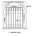
本実施例では、発光装置の電源供給線の主要部を埋め込み配線とする例を図3〜図6に示す。
【0047】
まず、上記実施の形態に従って、絶縁表面を有する基板上にエッチングストッパー層、該エッチングストッパー層を覆う珪素を主成分とする絶縁膜を形成し、該絶縁膜を選択的にエッチングして、エッチングストッパー層に達する開口(溝)を形成し、第1のバリア層を形成した後、電解メッキ処理を行って開口(溝)に十分な厚みの低抵抗金属膜を形成する。次いで、化学機械研磨法(以下、CMP法と呼ぶ)などで代表される平坦化処理を行い、開口(溝)だけに銅と第1のバリア層を残し、不要な部分を除去して埋め込み型の配線を形成する。この段階での上面図が図3に示した図であり、点線x−x’で切断した断面図が図1(C)に相当する。図3において、12は画素部、13はソース側駆動回路、14、15はゲート側駆動回路が配置される領域を示している。図3に示すように、電源供給線16の端部には電解メッキ処理を行う際に外部電源から電流を流すための接続電極パッドが基板の角に設けられている。なお、本実施例では、単色の発光素子をマトリクス状に配置する例とするため、電源供給線16は各画素に共通とし、全て導電位となるようにパターンが繋げられている。
【0048】
なお、簡略化のために電源供給線16は8本しか示していないが、実際は、m×n(m行n列)個の画素数を有している場合、電源供給線は、m本、もしくは電解メッキの均一性を上げるための予備配線を1、2本追加した本数となる。
【0049】
次いで、露出した銅の耐酸化性を高めるため、第2のバリア層を形成し、さらに下地絶縁膜として、AlNXOYで示される層を形成した後、酸化シリコン膜、窒化シリコン膜または酸化窒化シリコン膜などの絶縁膜の積層からなる下地絶縁膜を形成する。次いで、結晶質半導体膜を所望の形状にパターニングして半導体層を形成し、該半導体層を覆うゲート絶縁膜を形成する。
【0050】
次いで、埋め込み配線に達するコンタクトホールを形成した後、ゲート絶縁膜上にゲート配線、端子電極、および引き回し電極を形成する。この引き回し電極は、ソース側駆動回路13と画素部12との間に設け、後に形成するソース配線が引き回し配線(発光素子の陰極または陽極と接続する配線)17と重ならないように配置する電極である。また、端子電極は基板の端部に複数設け、そのうちのいくつかは埋め込み配線である電源供給線と接続させる。この段階での上面図が図4に示した図である。
【0051】
次いで、半導体にp型を付与する不純物元素(Bなど)またはn型を付与する不純物元素(P、As等)を適宜添加して、ソース領域及びドレイン領域を形成する。次いで、添加した不純物元素を活性化するために加熱処理、強光の照射、またはレーザー光の照射を行う。次いで、層間絶縁膜を形成し、水素化を行った後、ソース領域、ドレイン領域、引き回し電極、端子電極、または埋め込み配線に達するコンタクトホールを形成する。
【0052】
次いで、ソース電極(配線)、ドレイン電極、または接続電極を形成して各種TFTを完成させる。以上の工程が終了した段階で、画素部12においては、ソース領域と電源供給線とが電気的に接続され、ドレイン領域と接する接続電極(ここでは図示しない)が形成される。また、駆動回路においては、ソース領域に接するソース電極(配線)、ドレイン領域に接するドレイン電極が形成される。また、端子部においては、ある端子電極と接するソース配線、他の端子電極と接する引き回し配線(発光素子の陰極または陽極と接続する配線)17が形成される。また、駆動回路と画素部の間には、引き回し配線(発光素子の陰極または陽極と接続する配線)17が設けられる。この段階での上面図が図5に示した図である。
【0053】
次いで、画素部において、ドレイン領域と接する接続電極に接する第1の電極19をマトリクス状に配置する。この第1の電極19は、発光素子の陽極、或いは陰極となる。次いで、第1の電極19の端部を覆う絶縁物(バンク、隔壁、障壁、土手などと呼ばれる)を形成する。次いで、画素部に有機化合物を含む層10を形成し、その上に第2の電極11を形成して発光素子を完成させる。この第2の電極11は、発光素子の陰極、或いは陽極となる。なお、画素部とソース側駆動回路の間の領域で第2の電極11が、引き回し配線17と接して電気的接続させる。
【0054】
次いで、シール材31で基板と封止材(ここでは透光性を有する基板)30とを貼り合せる。この段階での上面図が図6に示した図である。さらに、外気を遮断するため、第2の電極11上に窒化シリコン膜、酸化窒化シリコン膜、またはDLC(ダイヤモンドライクカーボン)膜からなる保護膜を形成してもよい。最後に、端子電極に外部回路と接続するためのFPC(フレキシブルプリントサーキット)を貼り付ける。
【0055】
以上の工程でアクティブマトリクス型発光装置が完成する。
【0056】
なお、TFTを有するアクティブマトリクス型発光装置は、光の放射方向で2通りの構造が考えられる。一つは、発光素子からの発光が第2の電極を透過して放射されて観測者の目に入る構造である。この場合、観測者は第2の電極側から画像を認識することができる。もう一つは、発光素子からの発光が第1の電極および基板を透過して放射されて観測者の目に入る構造である。
【0057】
図2(A)に示すように発光素子からの発光が第2の電極を透過して放射されて観測者の目に入る構造とする場合、第2の電極11(図2(A)における電極119)は透光性を有する材料を用いることが望ましい。
【0058】
例えば、第1の電極19(図2(A)における電極117)を陽極とする場合、第1の電極19の材料として、仕事関数の大きい金属(Pt、Cr、W、Ni、Zn、Sn、In)を用い、端部を絶縁物(バンク、隔壁、障壁、土手などと呼ばれる)116で覆った後、正孔注入層として作用するポリ(エチレンジオキシチオフェン)/ポリ(スチレンスルホン酸)水溶液(PEDOT/PSS)を全面に塗布、焼成した後、発光層として作用する発光中心色素(1,1,4,4−テトラフェニル−1,3−ブタジエン(TPB)、4−ジシアノメチレン−2−メチル−6−(p−ジメチルアミノ−スチリル)−4H−ピラン(DCM1)、ナイルレッド、クマリン6など)ドープしたポリビニルカルバゾール(PVK)溶液を全面に塗布、焼成した後、仕事関数の小さい金属(Li、Mg、Cs)を含む薄膜と、その上に積層した透明導電膜(ITO(酸化インジウム酸化スズ合金)、酸化インジウム酸化亜鉛合金(In2O3―ZnO)、酸化亜鉛(ZnO)等)との積層からなる第2の電極11(図2(A)における電極119)を陰極として形成すればよい。なお、図2(A)においては、陰極の低抵抗化を図るため、絶縁物116上に補助電極120を設けている。こうして得られる発光素子は、白色発光を示す。なお、PEDOT/PSSは溶媒に水を用いており、有機溶剤には溶けない。従って、PVKをその上から塗布する場合にも、再溶解する心配はない。また、PEDOT/PSSとPVKは溶媒が異なるため、成膜室は同一のものを使用しないことが好ましい。なお、ここでは塗布により有機化合物を含む層10(図2(A)における118)を形成した例を示したが、特に限定されず、蒸着法により形成してもよい。
【0059】
また、上記例では図7(B)に示すように有機化合物層を積層とした例を示したが図7(A)に示すように有機化合物層を単層とすることもできる。例えば、ホール輸送性のポリビニルカルバゾール(PVK)に電子輸送性の1,3,4−オキサジアゾール誘導体(PBD)を分散させてもよい。また、30wt%のPBDを電子輸送剤として分散し、4種類の色素(TPB、クマリン6、DCM1、ナイルレッド)を適当量分散することで白色発光が得られる。また、図7(C)に示すように有機化合物層として高分子材料からなる層と、低分子材料からなる層とを積層してもよい。
【0060】
なお、有機化合物膜は、陽極と陰極の間に形成されており、陽極から注入された正孔と陰極から注入された電子が有機化合物膜において再結合することにより、有機化合物膜において、白色発光が得られる。
【0061】
また、赤色発光する有機化合物膜や緑色発光する有機化合物膜や青色発光する有機化合物膜を適宜選択し、重ねて混色させることによって全体として白色発光を得ることも可能である。
【0062】
白色発光を示す発光素子を形成し、フルカラー表示とするには様々な方法がある。例えば、図8(A)に示すように、得られた白色発光をカラーフィルターに通すことで赤、緑、青の発光を得るという方式(以下、カラーフィルター法とよぶ)がある。
【0063】
上記有機化合物膜が白色発光する方向に赤色発光以外を吸収する着色層(R)、緑色発光以外を吸収する着色層(G)、青色発光以外を吸収する着色層(B)をそれぞれ設けたカラーフィルタを形成することにより、発光素子からの白色発光をそれぞれ分離して、赤色発光、緑色発光、青色発光として得ることができる。また、アクティブマトリクス型の場合には、基板とカラーフィルターの間にTFTが形成される構造となる。また、カラーフィルターにおいて各着色層の間には遮光層が設けられており、大画面化する場合には、この遮光層に乾燥剤を含ませることが好ましい。
【0064】
また、着色層(R,G,B)には、最も単純なストライプパターンをはじめとして、斜めモザイク配列、三角モザイク配列、RGBG四画素配列、もしくはRGBW四画素配列などを用いることができる。
【0065】
白色光源(D65)を用いて各着色層の透過率と波長との関係の一例を図9に示した。カラーフィルターを構成する着色層は、顔料を分散した有機感光材料からなるカラーレジストを用いて形成される。また、白色発光とカラーフィルタを組み合わせた場合の色再現範囲を色度座標として図10に示す。なお、白色発光の色度座標は(x,y)=(0.34、0.35)である。図10よりフルカラーとしての色再現性は十分確保されていることが分かる。
【0066】
なお、この場合には、得られる発光色が異なっていても、すべて白色発光を示す有機化合物膜で形成されていることから、発光色ごとに有機化合物膜を塗り分けて形成する必要がない。また、鏡面反射を防ぐ円偏光板も特に必要ないものとすることができる。
【0067】
次に青色発光性の有機化合物膜を有する青色発光素子と蛍光性の色変換層を組み合わせることにより実現されるCCM法(color changing mediums)について図8(B)により説明する。
【0068】
CCM法は、青色発光素子から出射された青色発光で蛍光性の色変換層を励起し、それぞれの色変換層で色変換を行う。具体的には色変換層で青色から赤色への変換(B→R)、色変換層で青色から緑色への変換(B→G)、色変換層で青色から青色への変換(B→B)(なお、青色から青色への変換は行わなくても良い。)を行い、赤色、緑色及び青色の発光を得るというものである。CCM法の場合にも、アクティブマトリクス型の場合には、基板と色変換層の間にTFTが形成される構造となる。
【0069】
なお、この場合にも有機化合物膜を塗り分けて形成する必要がない。また、鏡面反射を防ぐ円偏光板も特に必要ないものとすることができる。
【0070】
また、CCM法を用いる場合には、色変換層が蛍光性であるため外光により励起され、コントラストを低下させる問題があるので、図8(C)に示したようにカラーフィルターを装着するなどしてコントラストを上げるようにすると良い。
【0071】
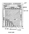
ここで、アクティブマトリクス型発光装置全体の外観図について図11に説明する。なお、図11(A)は、発光装置を示す上面図、図11(B)は図11(A)をA−A’で切断した断面図である。点線で示された901はソース信号線駆動回路、902は画素部、903はゲート信号線駆動回路である。また、904は封止基板、905はシール剤であり、シール剤905で囲まれた内側は、空間907になっている。
【0072】
なお、908はソース信号線駆動回路901及びゲート信号線駆動回路903に入力される信号を伝送するための配線であり、外部入力端子となるFPC(フレキシブルプリントサーキット)909からビデオ信号やクロック信号を受け取る。なお、ここではFPCしか図示されていないが、このFPCにはプリント配線基盤(PWB)が取り付けられていても良い。本明細書における発光装置には、発光装置本体だけでなく、それにFPCもしくはPWBが取り付けられた状態をも含むものとする。
【0073】
次に、断面構造について図11(B)を用いて説明する。基板910上には駆動回路及び画素部が形成されているが、ここでは、駆動回路としてソース信号線駆動回路901と画素部902が示されている。
【0074】
なお、ソース信号線駆動回路901はnチャネル型TFT923とpチャネル型TFT924とを組み合わせたCMOS回路が形成される。また、駆動回路を形成するTFTは、公知のCMOS回路、PMOS回路もしくはNMOS回路で形成しても良い。また、本実施の形態では、基板上に駆動回路を形成したドライバー一体型を示すが、必ずしもその必要はなく、基板上ではなく外部に形成することもできる。
【0075】
また、画素部902はスイッチング用TFT911と、電流制御用TFT912とそのドレインに電気的に接続された第1の電極(陽極)913を含む複数の画素により形成される。電流制御用TFT912のソースには、埋め込み配線930が電気的に接続されている。
【0076】
また、第1の電極(陽極)913の両端には絶縁層914が形成され、第1の電極(陽極)913上には有機化合物を含む層915が形成される。さらに、有機化合物を含む層915上には第2の電極(陰極)916が形成される。これにより、第1の電極(陽極)912、有機化合物を含む層915、及び第2の電極(陰極)916からなる発光素子918が形成される。ここでは発光素子918は白色発光とする例であるので着色層931とBM932からなるカラーフィルター(簡略化のため、ここではオーバーコート層は図示しない)が設けている。
【0077】
第2の電極(陰極)916は全画素に共通の配線としても機能し、接続配線908を経由してFPC909に電気的に接続されている。また、絶縁層914上には第3の電極(補助電極)が形成されており、第2の電極の低抵抗化を実現している。
【0078】
また、基板910上に形成された発光素子918を封止するためにシール剤905により封止基板904を貼り合わせる。なお、封止基板904と発光素子918との間隔を確保するために樹脂膜からなるスペーサを設けても良い。そして、シール剤905の内側の空間907には窒素等の不活性気体が充填されている。なお、シール剤905としてはエポキシ系樹脂を用いるのが好ましい。また、シール剤905はできるだけ水分や酸素を透過しない材料であることが望ましい。さらに、空間907の内部に酸素や水を吸収する効果をもつ物質を含有させても良い。
【0079】
また、本実施例では封止基板904を構成する材料としてガラス基板や石英基板の他、FRP(Fiberglass-Reinforced Plastics)、PVF(ポリビニルフロライド)、マイラー、ポリエステルまたはアクリル等からなるプラスチック基板を用いることができる。また、シール剤905を用いて封止基板904を接着した後、さらに側面(露呈面)を覆うようにシール剤で封止することも可能である。
【0080】
以上のようにして発光素子を空間907に封入することにより、発光素子を外部から完全に遮断することができ、外部から水分や酸素といった有機化合物層の劣化を促す物質が侵入することを防ぐことができる。従って、信頼性の高い発光装置を得ることができる。
【0081】
一方、図2(B)に示すように発光素子からの発光が第1の電極および基板を透過して放射されて観測者の目に入る構造とする場合、第1の電極19(図2(A)における電極117)は透光性を有する材料を用いることが望ましい。
【0082】
例えば、第1の電極19(図2(B)における電極117)を陽極とする場合、第1の電極19の材料として、透明導電膜(ITO(酸化インジウム酸化スズ合金)、酸化インジウム酸化亜鉛合金(In2O3―ZnO)、酸化亜鉛(ZnO)等)を用い、端部を絶縁物(バンク、隔壁、障壁、土手などと呼ばれる)116で覆った後、有機化合物を含む層118を形成し、その上に金属膜(MgAg、MgIn、AlLi、CaF2、CaNなどの合金、または周期表の1族もしくは2族に属する元素とアルミニウムとを共蒸着法により形成した膜)からなる第2の電極11(図2(B)における電極119)を陰極として形成すればよい。陰極形成の際には蒸着による抵抗加熱法を用い、蒸着マスクを用いて選択的に形成すればよい。
【0083】
また、本実施例は実施の形態と自由に組み合わせることができる。
【0084】
[実施例2]
ここでは液晶表示装置のゲート配線の主要部を埋め込み配線とする例を図12、図13に示す。
【0085】
まず、上記実施の形態に従って、絶縁表面を有する基板上にエッチングストッパー層、該エッチングストッパー層を覆う珪素を主成分とする絶縁膜を形成し、該絶縁膜を選択的にエッチングして、エッチングストッパー層に達する開口(溝)を形成し、第1のバリア層を形成した後、電解メッキ処理を行って開口(溝)に十分な厚みの低抵抗金属膜を形成する。次いで、化学機械研磨法(以下、CMP法と呼ぶ)などで代表される平坦化処理を行い、開口(溝)だけに銅と第1のバリア層を残し、不要な部分を除去して埋め込み型の配線を形成する。
【0086】
次いで、露出した銅の耐酸化性を高めるため、第2のバリア層を形成し、さらに下地絶縁膜として、AlNXOYで示される層を形成した後、酸化シリコン膜、窒化シリコン膜または酸化窒化シリコン膜などの絶縁膜の積層からなる下地絶縁膜を形成する。次いで、結晶質半導体膜を所望の形状にパターニングして半導体層を形成し、該半導体層を覆うゲート絶縁膜を形成する。
【0087】
次いで、埋め込み配線に達するコンタクトホールを形成した後、ゲート絶縁膜上にゲート電極、端子電極を形成する。なお、ゲート電極は、埋め込み配線と接続されてゲート配線の低抵抗化が実現する。また、端子電極は基板の端部に複数設ける。
【0088】
次いで、半導体にp型を付与する不純物元素(Bなど)またはn型を付与する不純物元素(P、As等)を適宜添加して、ソース領域及びドレイン領域を形成する。次いで、添加した不純物元素を活性化するために加熱処理、強光の照射、またはレーザー光の照射を行う。次いで、層間絶縁膜を形成し、水素化を行った後、ソース領域、ドレイン領域、端子電極に達するコンタクトホールを形成する。
【0089】
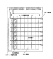
次いで、ソース電極(配線)55、またはドレイン電極を形成して各種TFTを完成させる。以上の工程が終了した段階で、画素部52においては、それぞれドレイン領域とドレイン電極とが電気的に接続され、ソース領域とソース電極(配線)とが電気的に接続される。また、駆動回路においては、ソース領域に接するソース電極(配線)、ドレイン領域に接するドレイン電極が形成される。また、端子部においては、ある端子電極と接するソース配線が形成される。次いで、画素部において、ドレイン領域と接する接続電極に接する画素電極59をマトリクス状に配置する。この段階での上面図が図13に示した図である。図13において、52は画素部、53はソース側駆動回路、54はゲート側駆動回路が配置される領域を示している。図13に示すように、ゲート配線56の端部には電解メッキ処理を行う際に外部電源から電流を流すための接続電極パッドが基板の端面近傍に設けられている。なお、本実施例では、ゲート配線56と同じ本数に対応する接続電極パッドを設けている。また、ゲート配線を全て導電位となるようにパターンを繋げてメッキ処理を行った後、分断して個々のゲート配線を形成してもよい。
【0090】
次いで、配向膜62aを形成した後、ラビング処理を行う。次いで、シール材(図示しない)で基板と対向基板60とを貼り合せ、基板間に液晶材料63を注入した後、封止する。対向基板60には予め、透明導電膜からなる対向電極61と、ラビング処理が行われた配向膜62bとが設けられている。最後に、端子電極に外部回路と接続するためのFPC(フレキシブルプリントサーキット)を貼り付け、さらに偏光板やカラーフィルターを設ける。
【0091】
以上の工程でアクティブマトリクス型液晶表示装置が完成する。
【0092】
なお、TFTを有するアクティブマトリクス型液晶表示装置は、3通りの構造(透過型、反射型、半透過型)が考えられる。画素電極を透明導電膜とし、バックライトを設ける透過型と、画素電極を反射金属膜とし、外光を反射させる反射型と、画素電極の一部を透明導電膜とし、その他の部分を反射金属膜として適宜切り替えを行う半透過型とがあるが、本発明は、いずれの構造に適用することができる。
【0093】
また、本実施例は実施の形態と自由に組み合わせることができる。
【0094】
[実施例3]
本発明を実施して形成された駆動回路や画素部は様々なモジュール(アクティブマトリクス型液晶モジュール、アクティブマトリクス型ECモジュール)を完成させることができる。即ち、本発明により、それらを表示部に組み込んだ電子機器全てを完成させることができる。
【0095】
その様な電子機器としては、ビデオカメラ、デジタルカメラ、ヘッドマウントディスプレイ(ゴーグル型ディスプレイ)、カーナビゲーション、プロジェクタ、カーステレオ、パーソナルコンピュータ、携帯情報端末(モバイルコンピュータ、携帯電話または電子書籍等)などが挙げられる。それらの一例を図14、図15に示す。
【0096】
図14(A)はパーソナルコンピュータであり、本体2001、画像入力部2002、表示部2003、キーボード2004等を含む。
【0097】
図14(B)はモバイルコンピュータ(モービルコンピュータ)であり、本体2201、カメラ部2202、受像部2203、操作スイッチ2204、表示部2205等を含む。
【0098】
図14(C)はプログラムを記録した記録媒体(以下、記録媒体と呼ぶ)を用いるプレーヤーであり、本体2401、表示部2402、スピーカ部2403、記録媒体2404、操作スイッチ2405等を含む。なお、このプレーヤーは記録媒体としてDVD(Digtial Versatile Disc)、CD等を用い、音楽鑑賞や映画鑑賞やゲームやインターネットを行うことができる。
【0099】
図15(A)は携帯書籍(電子書籍)であり、本体3001、表示部3002、3003、記憶媒体3004、操作スイッチ3005、アンテナ3006等を含む。
【0100】
図15(B)はディスプレイであり、本体3101、支持台3102、表示部3103等を含む。本発明は対角が10〜50インチの表示部3103を完成させることができる。
【0101】
以上の様に、本発明の適用範囲は極めて広く、あらゆる分野の電子機器を完成させることが可能である。また、本実施例の電子機器は実施の形態、実施例1、実施例2のどのような組み合わせからなる構成を用いても実現することができる。
【0102】
【発明の効果】
本発明により、アクティブマトリクス型の発光表示装置や液晶表示装置に代表される半導体装置において、画素部の面積が大きくなり大画面化しても良好な表示を実現することができる。画素部の配線の抵抗を大幅に低下させることができるため、例えば、対角40インチや対角50インチの大画面にも本発明は対応しうる。
【図面の簡単な説明】
【図1】 本発明の工程を示す断面図。(実施の形態)
【図2】 本発明の発光素子の断面を示す図。(実施例1)
【図3】 発光装置の作製過程における上面図を示す図。(実施例1)
【図4】 発光装置の作製過程における上面図を示す図。(実施例1)
【図5】 発光装置の作製過程における上面図を示す図。(実施例1)
【図6】 発光装置の作製過程における上面図を示す図。(実施例1)
【図7】 発光素子の積層構造を示す図。(実施例1)
【図8】 白色発光を用いてフルカラー化する場合の模式図である。(実施例1)
【図9】 着色層の透過率を示す図。(実施例1)
【図10】 色度座標を示す図。(実施例1)
【図11】 アクティブ型表示装置の断面図および上面図。(実施例1)
【図12】 液晶表示装置の断面図を示す図。(実施例2)
【図13】 液晶表示装置の作製過程における上面図を示す図。(実施例2)
【図14】 電子機器の一例を示す図。
【図15】 電子機器の一例を示す図。[0001]
BACKGROUND OF THE INVENTION
The present invention relates to a semiconductor device having a circuit formed of a thin film transistor (hereinafter referred to as TFT) and a manufacturing method thereof. For example, the present invention relates to an electronic apparatus in which an electro-optical device typified by a liquid crystal display device or a light emitting device having an OLED is mounted as a component.
[0002]
Note that in this specification, a semiconductor device refers to all devices that can function by utilizing semiconductor characteristics, and an electro-optical device, a semiconductor circuit, and an electronic device are all semiconductor devices.
[0003]
[Prior art]
In recent years, a technique for forming a thin film transistor (TFT) using a semiconductor thin film (having a thickness of about several to several hundred nm) formed on a substrate having an insulating surface has attracted attention. Thin film transistors are widely applied to electronic devices such as ICs and electro-optical devices, and development of switching devices for image display devices is urgently required.
[0004]
Conventionally, a liquid crystal display device is known as an image display device. Active matrix liquid crystal display devices are often used because high-definition images can be obtained compared to passive liquid crystal display devices. In an active matrix liquid crystal display device, a display pattern is formed on a screen by driving pixel electrodes arranged in a matrix. Specifically, by applying a voltage between the selected pixel electrode and the counter electrode corresponding to the pixel electrode, optical modulation of the liquid crystal layer disposed between the pixel electrode and the counter electrode is performed. The optical modulation is recognized by the observer as a display pattern.
[0005]
In addition, for a light emitting device using an OLED, a TFT is an essential element for realizing an active matrix driving method. Therefore, in a light emitting device using an OLED, at least a TFT that functions as a switching element and a TFT that supplies current to the OLED are provided in each pixel. A light-emitting element using an organic compound having characteristics such as thin and light weight, high-speed response, and direct current low-voltage driving as a light emitter is expected to be applied to a next-generation flat panel display. In particular, a display device in which light emitting elements are arranged in a matrix is considered to be superior to a conventional liquid crystal display device in that it has a wide viewing angle and excellent visibility.
[0006]
The light-emitting mechanism of the light-emitting element recombines electrons injected from the cathode and holes injected from the anode at the emission center in the organic compound layer by applying a voltage with the organic compound layer sandwiched between a pair of electrodes. Thus, it is said that molecular excitons are formed, and when the molecular excitons return to the ground state, energy is emitted and light is emitted. Singlet excitation and triplet excitation are known as excited states, and light emission is considered to be possible through either excited state.
[0007]
For a light-emitting device formed by arranging such light-emitting elements in a matrix, driving methods such as passive matrix driving (simple matrix type) and active matrix driving (active matrix type) can be used. However, when the pixel density increases, the active matrix type in which a switch is provided for each pixel (or one dot) is considered to be advantageous because it can be driven at a lower voltage.
[0008]
Applications of such active matrix display devices (typically liquid crystal display devices and light-emitting display devices) are expanding, and demands for higher definition, higher aperture ratio, and higher reliability as the screen size increases. Is growing. At the same time, demands for improved productivity and lower costs are increasing.
[0009]
[Problems to be solved by the invention]
Conventionally, when a TFT is manufactured using aluminum as the gate wiring material of the TFT, TFT malfunction and TFT characteristics are caused by the formation of protrusions such as hillocks and whiskers by heat treatment and diffusion of aluminum atoms into the channel formation region. Was causing a decline. Therefore, when using a metal material that can withstand heat treatment, typically a metal element having a high melting point, problems such as increased wiring resistance occur when the screen size is increased, resulting in increased power consumption. And so on.
[0010]
Therefore, an object of the present invention is to provide a structure of a semiconductor device that realizes low power consumption even when the screen is enlarged and a manufacturing method thereof.
[0011]
[Means for Solving the Problems]
In order to solve the above problems, the present invention forms an insulating layer and forms a buried wiring (such as Cu, Au, Ag, Ni, chromium, palladium, rhodium, tin, lead, or an alloy thereof) in the insulating layer. Further, after planarizing the surface of the insulating layer, a metal protective film (Ti, TiN, Ta, TaN, etc.) is formed on the exposed portion, and this embedded wiring is used as various wiring (gate wiring) of the light emitting device or the liquid crystal display device. , Source wiring, power supply line, common wiring, etc.) to reduce the resistance of the wiring. According to the present invention, low power consumption can be realized even when the screen size is increased.
[0012]
The configuration of the invention disclosed in this specification is, as shown in FIG.
Between the first substrate having an insulating surface and the second substrate having a light-transmitting property, a first electrode, a layer containing an organic compound in contact with the first electrode, and a layer containing the organic compound A light emitting device having a pixel portion having a plurality of light emitting elements having a second electrode in contact therewith, and a driving circuit having a thin film transistor,
In the light-emitting device, the gate wiring, the source wiring, or the power supply line arranged in the pixel portion is a buried wiring.
[0013]
In the above configuration, the embedded wiring is characterized by being copper, silver, gold, or an alloy thereof that can be plated. The embedded wiring is provided below the thin film transistor.
[0014]
In the above structure, the layer containing an organic compound is a material that emits white light, and is combined with a color filter provided on the second substrate. Alternatively, the layer containing an organic compound is a material that emits monochromatic light, and is characterized by being combined with a color conversion layer or a colored layer provided on the second substrate.
[0015]
The configuration of the invention for realizing the above structure is as follows.
A first step of forming a conductive etching stopper layer on the insulating surface;
A second step of forming a first insulating film covering the etching stopper layer;
Etching the first insulating film to form an opening reaching the etching stopper layer;
Forming a seed, plating, and forming a buried wiring covering the opening;
A fifth step of performing planarization;
A sixth step of forming a second insulating film containing aluminum;
A seventh step of forming a third insulating film on the second insulating film;
An eighth step of forming a semiconductor layer on the third insulating film;
A ninth step of forming a fourth insulating film on the semiconductor layer;
A tenth step of forming a gate electrode on the fourth insulating film;
An eleventh step of forming a wiring connected to the semiconductor layer and a wiring connected to the embedded wiring;
A twelfth step of forming a first electrode;
A method for manufacturing a light-emitting device, comprising: a layer containing an organic compound on the first electrode; and a thirteenth step of forming a second electrode on the layer containing the organic compound.
[0016]
In the structure related to the manufacturing method, the embedded wiring is a power supply line.
[0017]
In the structure related to the manufacturing method, the embedded wiring is copper, silver, gold, or an alloy thereof.
[0018]
Further, in the configuration relating to each of the above manufacturing methods, the etching stopper layer Plating may be performed using as a seed.
[0019]
In addition, as shown in FIG.
A pixel portion including a first electrode, a second electrode, and a liquid crystal material sandwiched between the first substrate having an insulating surface and the second substrate having a light-transmitting property; A liquid crystal display device having a driving circuit having a thin film transistor,
In the liquid crystal display device, the gate wiring or the source wiring arranged in the pixel portion is a buried wiring.
[0020]
In the above structure, the embedded wiring is copper, silver, gold, or an alloy thereof. In the above structure, the embedded wiring is provided below the thin film transistor.
[0021]
The configuration of the invention for realizing the above structure is as follows.
A first step of forming a conductive etching stopper layer on the insulating surface;
A second step of forming a first insulating film covering the etching stopper layer;
Etching the first insulating film to form an opening reaching the etching stopper layer;
Forming a seed, plating, and forming a buried wiring covering the opening;
A fifth step of performing planarization;
A sixth step of forming a second insulating film containing aluminum;
A seventh step of forming a third insulating film on the second insulating film;
An eighth step of forming a semiconductor layer on the third insulating film;
A ninth step of forming a fourth insulating film on the semiconductor layer;
A tenth step of forming a gate electrode on the fourth insulating film;
An eleventh step of forming a source wiring connected to the semiconductor layer and a wiring connecting the buried wiring and the gate electrode;
It is a manufacturing method of the liquid crystal display device characterized by having.
[0022]
In the structure related to the manufacturing method, the embedded wiring is a gate wiring. In the structure related to the manufacturing method, the embedded wiring is copper, silver, gold, or an alloy thereof.
[0023]
Note that the light-emitting element (EL element) includes a layer containing an organic compound (hereinafter, referred to as an EL layer) from which luminescence generated by applying an electric field is obtained, an anode, and a cathode. Luminescence in an organic compound includes light emission (fluorescence) when returning from a singlet excited state to a ground state and light emission (phosphorescence) when returning from a triplet excited state to a ground state, which are produced according to the present invention. The light emitting device can be applied to either light emission.
[0024]
The layer containing an organic compound has a laminated structure. Typically, a stacked structure of a hole transport layer / a light emitting layer / an electron transport layer is provided on the anode. This structure has very high luminous efficiency, and most of the light emitting devices that are currently under research and development employ this structure. In addition, a hole injection layer / a hole transport layer / a light emitting layer / an electron transport layer, or a hole injection layer / a hole transport layer / a light emitting layer / an electron transport layer / an electron injection layer are sequentially laminated on the anode. Good structure. You may dope a fluorescent pigment | dye etc. with respect to a light emitting layer. These layers may all be formed using a low molecular weight material, or may be formed using a high molecular weight material. Note that in this specification, all layers provided between a cathode and an anode are collectively referred to as a layer containing an organic compound (EL layer). Therefore, the hole injection layer, the hole transport layer, the light emitting layer, the electron transport layer, and the electron injection layer are all included in the EL layer. The layer containing an organic compound (EL layer) may also contain an inorganic material such as silicon.
[0025]
In the light emitting device of the present invention, the screen display driving method is not particularly limited, and for example, a dot sequential driving method, a line sequential driving method, a surface sequential driving method, or the like may be used. Typically, a line sequential driving method is used, and a time-division gray scale driving method or an area gray scale driving method may be used as appropriate. The video signal input to the source line of the light-emitting device may be an analog signal or a digital signal, and a drive circuit or the like may be designed in accordance with the video signal as appropriate.
[0026]
DETAILED DESCRIPTION OF THE INVENTION
Embodiments of the present invention will be described below.
[0027]
Here, FIG. 1 shows an example in which a buried wiring and a TFT are formed.
[0028]
First, the
[0029]
Next, patterning is performed, and the insulating
[0030]
Next, by performing a planarization process represented by a chemical mechanical polishing method (hereinafter referred to as a CMP method), copper and the first barrier layer are left only in the openings (grooves), and unnecessary portions are removed. Embedded wirings (hereinafter referred to as embedded wirings) 104a and 104b are formed. (Fig. 1 (B))
[0031]
Next, a
[0032]
Next, AlN is used as a base insulating film for preventing impurity diffusion into the TFT formed later. X O Y The
[0033]
Next, a base insulating film 108 including a stack of insulating films such as a silicon oxide film, a silicon nitride film, or a silicon oxynitride film is formed. Although a two-layer structure is used here as the base insulating film 108, a single-layer film of the insulating film or a structure in which two or more layers are stacked may be used. As the
[0034]
Next, a semiconductor layer is formed over the base film. The semiconductor layer is formed by forming a semiconductor film having an amorphous structure by a known means (sputtering method, LPCVD method, plasma CVD method, etc.), and then known crystallization treatment (laser crystallization method, thermal crystallization method). Or a crystalline semiconductor film obtained by performing a thermal crystallization method using a catalyst such as nickel) is formed into a desired shape by patterning. The semiconductor layer is formed with a thickness of 25 to 80 nm (preferably 30 to 60 nm). There is no limitation on the material of the crystalline semiconductor film, but it is preferably formed of silicon or a silicon germanium alloy.
[0035]
When a crystalline semiconductor film is formed by laser crystallization, a pulse oscillation type or continuous emission type excimer laser, YAG laser, YVO Four A laser can be used. When these lasers are used, it is preferable to use a method in which laser light emitted from a laser oscillator is linearly collected by an optical system and irradiated onto a semiconductor film. Crystallization conditions are appropriately selected by the practitioner. When an excimer laser is used, the pulse oscillation frequency is 30 Hz and the laser energy density is 100 to 400 mJ / cm. 2 (Typically 200-300mJ / cm 2 ). When a YAG laser is used, the second harmonic is used and the pulse oscillation frequency is 1 to 10 kHz, and the laser energy density is 300 to 600 mJ / cm. 2 (Typically 350-500mJ / cm 2 ) Then, when the laser beam condensed linearly with a width of 100 to 1000 μm, for example, 400 μm is irradiated over the entire surface of the substrate, the superposition ratio (overlap ratio) of the linear laser light at this time is 80 to 98%. Good.
[0036]
Next, the surface of the semiconductor layer is washed with an etchant containing hydrofluoric acid to form a
[0037]
Next, after cleaning the surface of the
[0038]
Next, an impurity element imparting p-type conductivity to the semiconductor (such as B), here boron, is added as appropriate, so that the
[0039]
In the subsequent steps, an
[0040]
The TFTs having the embedded
[0041]
Here, although the embedded
[0042]
Further, the present invention is not limited to the TFT structure of FIG. 1E, and if necessary, a lightly doped drain (LDD) having an LDD region between a channel formation region and a drain region (or source region). ) Structure may be used. In this structure, a region to which an impurity element is added at a low concentration is provided between a channel formation region and a source region or a drain region formed by adding an impurity element at a high concentration, and this region is referred to as an LDD region. I'm calling. Further, a so-called GOLD (Gate-drain Overlapped LDD) structure in which an LDD region is disposed so as to overlap with a gate electrode through a gate insulating film may be employed.
[0043]
In addition, although a p-channel TFT has been described here, an n-type impurity element (P, As, etc.) is used instead of the p-type impurity element. n Needless to say, a channel TFT can be formed.
[0044]
Although the top gate type TFT has been described as an example here, the present invention can be applied regardless of the TFT structure. For example, it can be applied to a bottom gate type (reverse stagger type) TFT or a forward stagger type TFT. Is possible.
[0045]
The present invention having the above-described configuration will be described in more detail with the following examples.
[0046]
(Example)
[Example 1]
In this embodiment, an example in which the main part of the power supply line of the light emitting device is embedded wiring is shown in FIGS.
[0047]
First, according to the above embodiment, an etching stopper layer and an insulating film mainly composed of silicon covering the etching stopper layer are formed on a substrate having an insulating surface, and the insulating film is selectively etched to form an etching stopper. After forming an opening (groove) reaching the layer and forming the first barrier layer, electrolytic plating is performed to form a low-resistance metal film having a sufficient thickness in the opening (groove). Next, a planarization process represented by a chemical mechanical polishing method (hereinafter referred to as a CMP method) is performed, leaving copper and the first barrier layer only in the opening (groove), and removing unnecessary portions to embed the mold. The wiring is formed. A top view at this stage is shown in FIG. 3, and a cross-sectional view taken along a dotted line xx ′ corresponds to FIG. In FIG. 3, reference numeral 12 denotes a pixel portion, 13 denotes a source side driver circuit, and 14 and 15 denote regions where gate side driver circuits are arranged. As shown in FIG. 3, connection electrode pads are provided at the corners of the substrate at the end portions of the
[0048]
For simplification, only eight
[0049]
Next, in order to increase the oxidation resistance of the exposed copper, a second barrier layer is formed, and further, AlN is used as a base insulating film. X O Y Then, a base insulating film formed by stacking insulating films such as a silicon oxide film, a silicon nitride film, or a silicon oxynitride film is formed. Next, the crystalline semiconductor film is patterned into a desired shape to form a semiconductor layer, and a gate insulating film covering the semiconductor layer is formed.
[0050]
Next, after forming a contact hole reaching the buried wiring, a gate wiring, a terminal electrode, and a routing electrode are formed on the gate insulating film. This routing electrode is an electrode provided between the source side driving circuit 13 and the pixel portion 12 and arranged so that a source wiring to be formed later does not overlap with the routing wiring (wiring connected to the cathode or anode of the light emitting element) 17. is there. A plurality of terminal electrodes are provided at the end of the substrate, some of which are connected to power supply lines which are embedded wirings. FIG. 4 is a top view at this stage.
[0051]
Next, an impurity element that imparts p-type conductivity (such as B) or an impurity element that imparts n-type conductivity (such as P or As) to the semiconductor is added as appropriate to form source and drain regions. Next, heat treatment, intense light irradiation, or laser light irradiation is performed to activate the added impurity element. Next, after forming an interlayer insulating film and performing hydrogenation, contact holes reaching the source region, the drain region, the lead-out electrode, the terminal electrode, or the buried wiring are formed.
[0052]
Next, a source electrode (wiring), a drain electrode, or a connection electrode is formed to complete various TFTs. At the stage where the above steps are completed, in the pixel portion 12, the source region and the power supply line are electrically connected, and a connection electrode (not shown here) in contact with the drain region is formed. In the driver circuit, a source electrode (wiring) in contact with the source region and a drain electrode in contact with the drain region are formed. In the terminal portion, a source wiring in contact with a certain terminal electrode and a routing wiring (wiring connected to the cathode or anode of the light emitting element) 17 in contact with another terminal electrode are formed. A lead wiring (wiring connected to the cathode or anode of the light emitting element) 17 is provided between the driving circuit and the pixel portion. FIG. 5 is a top view at this stage.
[0053]
Next, in the pixel portion, the first electrodes 19 in contact with the connection electrodes in contact with the drain region are arranged in a matrix. The first electrode 19 serves as an anode or a cathode of the light emitting element. Next, an insulator (referred to as a bank, a partition, a barrier, a bank, or the like) that covers the end portion of the first electrode 19 is formed. Next, a
[0054]
Next, the substrate and the sealing material (translucent substrate here) 30 are bonded to each other with the sealing material 31. FIG. 6 is a top view at this stage. Further, a protective film made of a silicon nitride film, a silicon oxynitride film, or a DLC (diamond-like carbon) film may be formed over the second electrode 11 in order to block outside air. Finally, an FPC (flexible printed circuit) for connecting to an external circuit is attached to the terminal electrode.
[0055]
The active matrix light emitting device is completed through the above steps.
[0056]
Note that an active matrix light-emitting device having a TFT can have two structures in the light emission direction. One is a structure in which light emitted from the light emitting element is emitted through the second electrode and enters the observer's eyes. In this case, the observer can recognize the image from the second electrode side. The other is a structure in which light emitted from the light-emitting element is emitted through the first electrode and the substrate and enters the observer's eyes.
[0057]
As shown in FIG. 2A, in the case where light emitted from the light-emitting element is emitted through the second electrode and enters the observer's eyes, the second electrode 11 (the electrode in FIG. 2A) is used. 119) preferably uses a light-transmitting material.
[0058]
For example, when the first electrode 19 (the
[0059]
In the above example, an example in which an organic compound layer is stacked as shown in FIG. 7B is shown, but the organic compound layer can be a single layer as shown in FIG. 7A. For example, an electron transporting 1,3,4-oxadiazole derivative (PBD) may be dispersed in hole transporting polyvinyl carbazole (PVK). Further, white light emission can be obtained by dispersing 30 wt% PBD as an electron transporting agent and dispersing an appropriate amount of four kinds of dyes (TPB, coumarin 6, DCM1, Nile red). Further, as shown in FIG. 7C, a layer made of a high molecular material and a layer made of a low molecular material may be stacked as the organic compound layer.
[0060]
The organic compound film is formed between the anode and the cathode, and the holes injected from the anode and the electrons injected from the cathode are recombined in the organic compound film, so that the organic compound film emits white light. Is obtained.
[0061]
It is also possible to obtain white light emission as a whole by appropriately selecting an organic compound film emitting red light, an organic compound film emitting green light, or an organic compound film emitting blue light and mixing them in layers.
[0062]
There are various methods for forming a light emitting element that emits white light to achieve full color display. For example, as shown in FIG. 8A, there is a method of obtaining red, green, and blue light emission by passing the obtained white light emission through a color filter (hereinafter referred to as a color filter method).
[0063]
A color provided with a colored layer (R) that absorbs light other than red light, a colored layer (G) that absorbs light other than green light, and a colored layer (B) that absorbs light other than blue light in the direction in which the organic compound film emits white light. By forming the filter, white light emission from the light emitting element can be separated and obtained as red light emission, green light emission, and blue light emission. In the case of the active matrix type, a TFT is formed between the substrate and the color filter. In the color filter, a light shielding layer is provided between the colored layers, and when the screen is enlarged, it is preferable to include a desiccant in the light shielding layer.
[0064]
In addition, the colored layer (R, G, B) can use a simplest stripe pattern, an oblique mosaic arrangement, a triangular mosaic arrangement, an RGBG four-pixel arrangement, or an RGBW four-pixel arrangement.
[0065]
An example of the relationship between the transmittance and wavelength of each colored layer using a white light source (D65) is shown in FIG. The colored layer constituting the color filter is formed using a color resist made of an organic photosensitive material in which a pigment is dispersed. FIG. 10 shows the color reproduction range when white light emission and a color filter are combined as chromaticity coordinates. The chromaticity coordinates of white light emission are (x, y) = (0.34, 0.35). FIG. 10 shows that the color reproducibility as a full color is sufficiently secured.
[0066]
In this case, even if the luminescent color obtained is different, all the organic compound films exhibiting white luminescence are formed, so that it is not necessary to separately form the organic compound film for each luminescent color. Further, a circularly polarizing plate that prevents specular reflection can be omitted.
[0067]
Next, a CCM method (color changing mediums) realized by combining a blue light emitting element having a blue light emitting organic compound film and a fluorescent color conversion layer will be described with reference to FIG.
[0068]
In the CCM method, blue light emitted from a blue light emitting element excites a fluorescent color conversion layer, and color conversion is performed in each color conversion layer. Specifically, the color conversion layer converts blue to red (B → R), the color conversion layer converts blue to green (B → G), and the color conversion layer converts blue to blue (B → B). ) (Note that the conversion from blue to blue is not necessary) to obtain red, green and blue light emission. Also in the case of the CCM method, the active matrix type has a structure in which TFTs are formed between the substrate and the color conversion layer.
[0069]
In this case, it is not necessary to form the organic compound film separately. Further, a circularly polarizing plate that prevents specular reflection can be omitted.
[0070]
Further, when the CCM method is used, since the color conversion layer is fluorescent, it is excited by external light and has a problem of lowering the contrast. Therefore, a color filter is attached as shown in FIG. To increase the contrast.
[0071]
Here, an external view of the entire active matrix light-emitting device will be described with reference to FIG. 11A is a top view illustrating the light-emitting device, and FIG. 11B is a cross-sectional view taken along line AA ′ in FIG. 11A. Reference numeral 901 indicated by a dotted line denotes a source signal line driver circuit, 902 denotes a pixel portion, and 903 denotes a gate signal line driver circuit. Reference numeral 904 denotes a sealing substrate, reference numeral 905 denotes a sealant, and the inside surrounded by the sealant 905 is a space 907.
[0072]
Note that reference numeral 908 denotes wiring for transmitting signals input to the source signal line driver circuit 901 and the gate signal line driver circuit 903, and a video signal and a clock signal are received from an FPC (flexible printed circuit) 909 serving as an external input terminal. receive. Although only the FPC is shown here, a printed wiring board (PWB) may be attached to the FPC. The light-emitting device in this specification includes not only a light-emitting device body but also a state in which an FPC or a PWB is attached thereto.
[0073]
Next, a cross-sectional structure is described with reference to FIG. A driver circuit and a pixel portion are formed over the substrate 910. Here, a source signal line driver circuit 901 and a pixel portion 902 are shown as the driver circuits.
[0074]
Note that as the source signal line driver circuit 901, a CMOS circuit in which an n-
[0075]
The pixel portion 902 is formed by a plurality of pixels including a switching
[0076]
An insulating layer 914 is formed on both ends of the first electrode (anode) 913, and a
[0077]
The second electrode (cathode) 916 also functions as a wiring common to all pixels, and is electrically connected to the
[0078]
In addition, in order to seal the light emitting element 918 formed over the substrate 910, the sealing substrate 904 is attached with a sealant 905. Note that a spacer made of a resin film may be provided in order to secure a space between the sealing substrate 904 and the light-emitting element 918. A space 907 inside the sealing agent 905 is filled with an inert gas such as nitrogen. Note that an epoxy resin is preferably used as the sealant 905. In addition, the sealant 905 is desirably a material that does not transmit moisture and oxygen as much as possible. Furthermore, a substance having an effect of absorbing oxygen and water may be contained in the space 907.
[0079]
Further, in this embodiment, a plastic substrate made of FRP (Fiberglass-Reinforced Plastics), PVF (polyvinyl fluoride), Mylar, polyester, acrylic, or the like is used as a material constituting the sealing substrate 904 as a material constituting the sealing substrate 904. be able to. In addition, after the sealing substrate 904 is bonded using the sealing agent 905, the sealing substrate 904 can be further sealed with a sealing agent so as to cover the side surface (exposed surface).
[0080]
By encapsulating the light emitting element in the space 907 as described above, the light emitting element can be completely blocked from the outside, and a substance that promotes deterioration of the organic compound layer such as moisture and oxygen can be prevented from entering from the outside. Can do. Therefore, a highly reliable light-emitting device can be obtained.
[0081]
On the other hand, as shown in FIG. 2B, when the light emitted from the light-emitting element is emitted through the first electrode and the substrate and enters the eyes of the observer, the first electrode 19 (FIG. 2B The electrode 117) in A) is preferably made of a light-transmitting material.
[0082]
For example, when the first electrode 19 (
[0083]
This embodiment can be freely combined with the embodiment mode.
[0084]
[Example 2]
Here, an example in which the main part of the gate wiring of the liquid crystal display device is a buried wiring is shown in FIGS.
[0085]
First, according to the above embodiment, an etching stopper layer and an insulating film mainly composed of silicon covering the etching stopper layer are formed on a substrate having an insulating surface, and the insulating film is selectively etched to form an etching stopper. After forming an opening (groove) reaching the layer and forming the first barrier layer, electrolytic plating is performed to form a low-resistance metal film having a sufficient thickness in the opening (groove). Next, a planarization process represented by a chemical mechanical polishing method (hereinafter referred to as a CMP method) is performed, leaving copper and the first barrier layer only in the opening (groove), and removing unnecessary portions to embed the mold. The wiring is formed.
[0086]
Next, in order to increase the oxidation resistance of the exposed copper, a second barrier layer is formed, and further, AlN is used as a base insulating film. X O Y Then, a base insulating film formed by stacking insulating films such as a silicon oxide film, a silicon nitride film, or a silicon oxynitride film is formed. Next, the crystalline semiconductor film is patterned into a desired shape to form a semiconductor layer, and a gate insulating film covering the semiconductor layer is formed.
[0087]
Next, after forming a contact hole reaching the buried wiring, a gate electrode and a terminal electrode are formed on the gate insulating film. Note that the gate electrode is connected to the buried wiring, and the resistance of the gate wiring is reduced. A plurality of terminal electrodes are provided at the end of the substrate.
[0088]
Next, an impurity element that imparts p-type conductivity (such as B) or an impurity element that imparts n-type conductivity (such as P or As) to the semiconductor is added as appropriate to form source and drain regions. Next, heat treatment, intense light irradiation, or laser light irradiation is performed to activate the added impurity element. Next, an interlayer insulating film is formed, hydrogenated, and contact holes reaching the source region, the drain region, and the terminal electrode are formed.
[0089]
Next, a source electrode (wiring) 55 or a drain electrode is formed to complete various TFTs. When the above steps are completed, in the pixel portion 52, the drain region and the drain electrode are electrically connected, and the source region and the source electrode (wiring) are electrically connected. In the driver circuit, a source electrode (wiring) in contact with the source region and a drain electrode in contact with the drain region are formed. In the terminal portion, a source wiring that contacts a certain terminal electrode is formed. Next, in the pixel portion,
[0090]
Next, after the
[0091]
The active matrix liquid crystal display device is completed through the above steps.
[0092]
Note that three types of structures (transmission type, reflection type, and transflective type) can be considered for an active matrix liquid crystal display device having TFTs. The pixel electrode is a transparent conductive film, a transmissive type with a backlight, the pixel electrode is a reflective metal film, the reflective type reflects external light, and a part of the pixel electrode is a transparent conductive film, and the other part is a reflective metal. There is a transflective type in which the film is switched as appropriate, but the present invention can be applied to any structure.
[0093]
This embodiment can be freely combined with the embodiment mode.
[0094]
[Example 3]
Various modules (active matrix type liquid crystal module, active matrix type EC module) can be completed in the driver circuit and the pixel portion formed by implementing the present invention. That is, according to the present invention, all electronic devices in which they are incorporated into the display portion can be completed.
[0095]
Such electronic devices include video cameras, digital cameras, head mounted displays (goggles type displays), car navigation systems, projectors, car stereos, personal computers, personal digital assistants (mobile computers, mobile phones, electronic books, etc.), etc. Can be mentioned. Examples of these are shown in FIGS.
[0096]
FIG. 14A illustrates a personal computer, which includes a main body 2001, an image input portion 2002, a display portion 2003, a
[0097]
FIG. 14B shows a mobile computer, which includes a main body 2201, a camera unit 2202, an
[0098]
FIG. 14C shows a player using a recording medium (hereinafter referred to as a recording medium) on which a program is recorded, and includes a main body 2401, a
[0099]
FIG. 15A illustrates a portable book (electronic book), which includes a
[0100]
FIG. 15B shows a display, which includes a
[0101]
As described above, the applicable range of the present invention is so wide that electronic devices in various fields can be completed. In addition, the electronic apparatus of this example can be realized by using a configuration including any combination of the embodiment mode, the first example, and the second example.
[0102]
【The invention's effect】
According to the present invention, in a semiconductor device typified by an active matrix light-emitting display device or a liquid crystal display device, an excellent display can be realized even if the area of a pixel portion is increased and the screen size is increased. Since the resistance of the wiring of the pixel portion can be greatly reduced, the present invention can be applied to, for example, a large screen with a diagonal of 40 inches or a diagonal of 50 inches.
[Brief description of the drawings]
FIG. 1 is a cross-sectional view showing a process of the present invention. (Embodiment)
FIG. 2 is a cross-sectional view of a light emitting element of the present invention. (Example 1)
FIGS. 3A and 3B are top views of a light-emitting device in the manufacturing process. FIGS. (Example 1)
FIGS. 4A and 4B are top views of a manufacturing process of a light-emitting device. FIGS. (Example 1)
FIGS. 5A and 5B are top views of a manufacturing process of a light-emitting device. FIGS. (Example 1)
FIGS. 6A and 6B are top views of a manufacturing process of a light-emitting device. FIGS. (Example 1)
FIG 7 illustrates a stacked structure of a light-emitting element. (Example 1)
FIG. 8 is a schematic diagram in the case of full color using white light emission. (Example 1)
FIG. 9 is a graph showing the transmittance of a colored layer. (Example 1)
FIG. 10 is a diagram showing chromaticity coordinates. (Example 1)
11A and 11B are a cross-sectional view and a top view of an active display device. (Example 1)
FIG. 12 is a cross-sectional view of a liquid crystal display device. (Example 2)
FIG. 13 is a top view of a manufacturing process of a liquid crystal display device. (Example 2)
FIG 14 illustrates an example of an electronic device.
FIG 15 illustrates an example of an electronic device.
Claims (16)
前記基板上の第1の絶縁膜と、
前記第1の絶縁膜に埋め込まれた配線と、
前記第1の絶縁膜及び前記配線上の第2の絶縁膜と、
前記第2の絶縁膜上の薄膜トランジスタとを有し、
前記薄膜トランジスタは半導体層、ゲート絶縁膜、及びゲート電極を有し、
前記配線は、銅、銀、金、クロム、鉄、ニッケル、白金、またはこれらの合金でなり、
前記配線と前記第1の絶縁膜の間及び前記配線と前記第2の絶縁膜の間にはバリア層が設けられ、前記バリア層は前記配線と接しており、
前記薄膜トランジスタの前記ゲート電極は前記配線と電気的に接続していることを特徴とする半導体装置。A substrate having an insulating surface;
A first insulating film on the substrate;
A wiring embedded in the first insulating film;
A first insulating film and a second insulating film on the wiring;
A thin film transistor on the second insulating film,
The thin film transistor has a semiconductor layer, a gate insulating film, and a gate electrode,
The wiring is made of copper, silver, gold, chromium, iron, nickel, platinum, or an alloy thereof,
A barrier layer is provided between the wiring and the first insulating film and between the wiring and the second insulating film, and the barrier layer is in contact with the wiring,
The semiconductor device, wherein the gate electrode of the thin film transistor is electrically connected to the wiring.
前記基板上の第1の絶縁膜と、
前記第1の絶縁膜に埋め込まれた配線と、
前記第1の絶縁膜及び前記配線上の第2の絶縁膜と、
前記第2の絶縁膜上の薄膜トランジスタとを有し、
前記薄膜トランジスタは、ソース領域及びドレイン領域を有する半導体層、ゲート絶縁膜、並びにゲート電極を有し、
前記配線は、銅、銀、金、クロム、鉄、ニッケル、白金、またはこれらの合金でなり、
前記配線と前記第1の絶縁膜の間及び前記配線と前記第2の絶縁膜の間にはバリア層が設けられ、前記バリア層は前記配線と接しており、
前記薄膜トランジスタの前記ソース領域は前記配線と電気的に接続していることを特徴とする半導体装置。A substrate having an insulating surface;
A first insulating film on the substrate;
A wiring embedded in the first insulating film;
A first insulating film and a second insulating film on the wiring;
A thin film transistor on the second insulating film,
The thin film transistor includes a semiconductor layer having a source region and a drain region, a gate insulating film, and a gate electrode,
The wiring is made of copper, silver, gold, chromium, iron, nickel, platinum, or an alloy thereof,
A barrier layer is provided between the wiring and the first insulating film and between the wiring and the second insulating film, and the barrier layer is in contact with the wiring,
The semiconductor device is characterized in that the source region of the thin film transistor is electrically connected to the wiring.
前記基板上の第1の絶縁膜と、
前記第1の絶縁膜に埋め込まれた配線と、
前記第1の絶縁膜及び前記配線上の第2の絶縁膜と、
前記第2の絶縁膜上の薄膜トランジスタとを有し、
前記薄膜トランジスタは、ソース領域及びドレイン領域を有する半導体層、ゲート絶縁膜、並びにゲート電極を有し、
前記配線は、銅、銀、金、クロム、鉄、ニッケル、白金、またはこれらの合金でなり、
前記配線と前記第1の絶縁膜の間及び前記配線と前記第2の絶縁膜の間にはバリア層が設けられ、前記バリア層は前記配線と接しており、
前記薄膜トランジスタの前記ドレイン領域は前記配線と電気的に接続していることを特徴とする半導体装置。A substrate having an insulating surface;
A first insulating film on the substrate;
A wiring embedded in the first insulating film;
A first insulating film and a second insulating film on the wiring;
A thin film transistor on the second insulating film,
The thin film transistor includes a semiconductor layer having a source region and a drain region, a gate insulating film, and a gate electrode,
The wiring is made of copper, silver, gold, chromium, iron, nickel, platinum, or an alloy thereof,
A barrier layer is provided between the wiring and the first insulating film and between the wiring and the second insulating film, and the barrier layer is in contact with the wiring,
The semiconductor device, wherein the drain region of the thin film transistor is electrically connected to the wiring.
前記配線はゲート配線であることを特徴とする半導体装置。The semiconductor device, wherein the wiring is a gate wiring.
前記配線は、ソース配線、または電源供給線であることを特徴とする半導体装置。The semiconductor device is characterized in that the wiring is a source wiring or a power supply line.
前記基板上の第1の絶縁膜と、A first insulating film on the substrate;
前記第1の絶縁膜に埋め込まれたゲート配線と、A gate wiring embedded in the first insulating film;
前記第1の絶縁膜及び前記ゲート配線上の第2の絶縁膜と、A second insulating film on the first insulating film and the gate wiring;
前記第2の絶縁膜上の薄膜トランジスタとを有し、A thin film transistor on the second insulating film,
前記薄膜トランジスタは半導体層、ゲート絶縁膜、及びゲート電極を有し、The thin film transistor has a semiconductor layer, a gate insulating film, and a gate electrode,
前記ゲート配線は、銅、銀、金、クロム、鉄、ニッケル、白金、またはこれらの合金でなり、The gate wiring is made of copper, silver, gold, chromium, iron, nickel, platinum, or an alloy thereof.
前記薄膜トランジスタの前記ゲート電極は前記ゲート配線と電気的に接続していることを特徴とする半導体装置。The semiconductor device, wherein the gate electrode of the thin film transistor is electrically connected to the gate wiring.
前記基板上の第1の絶縁膜と、A first insulating film on the substrate;
前記第1の絶縁膜に埋め込まれた電源供給線と、A power supply line embedded in the first insulating film;
前記第1の絶縁膜及び前記電源供給線上の第2の絶縁膜と、The first insulating film and the second insulating film on the power supply line;
前記第2の絶縁膜上の薄膜トランジスタとを有し、A thin film transistor on the second insulating film,
前記薄膜トランジスタは、ソース領域及びドレイン領域を有する半導体層、ゲート絶縁膜、並びにゲート電極を有し、The thin film transistor includes a semiconductor layer having a source region and a drain region, a gate insulating film, and a gate electrode,
前記電源供給線は、銅、銀、金、クロム、鉄、ニッケル、白金、またはこれらの合金でなり、The power supply line is made of copper, silver, gold, chromium, iron, nickel, platinum, or an alloy thereof.
前記薄膜トランジスタの前記ソース領域は前記電源供給線と電気的に接続していることを特徴とする半導体装置。The semiconductor device, wherein the source region of the thin film transistor is electrically connected to the power supply line.
前記基板上に形成され、第1の電極、有機化合物を含む層、第2の電極を順に積層してなる発光素子と、前記基板に貼り合わされた、前記発光素子を封止する封止基板とを有することを特徴とする半導体装置。In any one of Claims 1 thru | or 7 ,
A light-emitting element formed on the substrate, in which a first electrode, a layer containing an organic compound, and a second electrode are sequentially stacked; and a sealing substrate that is bonded to the substrate and seals the light-emitting element; A semiconductor device comprising:
前記エッチングストッパー層を覆う第1の絶縁膜を形成し、
前記第1の絶縁膜にエッチングを行い、前記エッチングストッパー層に達する開口を形成し、
前記開口にシードを形成し、
前記シードにメッキを行い、前記開口を覆う埋め込み配線を形成し、
平坦化処理を行い、前記第1の絶縁膜の上面と前記埋め込み配線の上面を平坦にし、
前記第1の絶縁膜及び前記埋め込み配線上にアルミニウムを含む第2の絶縁膜を形成し、
前記第2の絶縁膜上に第3の絶縁膜を形成し、
前記第3の絶縁膜上に、ソース領域及びドレイン領域を有する半導体層、ゲート絶縁膜並びにゲート電極を有する薄膜トランジスタを形成し、
前記ソース領域、前記ドレイン領域、または前記ゲート電極は、前記埋め込み配線と電気的に接続していることを特徴とする半導体装置の作製方法。Forming a conductive etching stopper layer on the insulating surface;
Forming a first insulating film covering the etching stopper layer;
Etching the first insulating film to form an opening reaching the etching stopper layer;
Forming a seed in the opening;
Plating the seed, forming an embedded wiring covering the opening;
Performing a planarization process to planarize the upper surface of the first insulating film and the upper surface of the embedded wiring;
Forming a second insulating film containing aluminum on the first insulating film and the embedded wiring;
Forming a third insulating film on the second insulating film;
A thin film transistor having a semiconductor layer having a source region and a drain region, a gate insulating film, and a gate electrode is formed on the third insulating film,
The method for manufacturing a semiconductor device, wherein the source region, the drain region, or the gate electrode is electrically connected to the embedded wiring.
Priority Applications (1)
| Application Number | Priority Date | Filing Date | Title |
|---|---|---|---|
| JP2003084808A JP4339000B2 (en) | 2002-03-26 | 2003-03-26 | Semiconductor device and manufacturing method thereof |
Applications Claiming Priority (2)
| Application Number | Priority Date | Filing Date | Title |
|---|---|---|---|
| JP2002087222 | 2002-03-26 | ||
| JP2003084808A JP4339000B2 (en) | 2002-03-26 | 2003-03-26 | Semiconductor device and manufacturing method thereof |
Publications (3)
| Publication Number | Publication Date |
|---|---|
| JP2004004663A JP2004004663A (en) | 2004-01-08 |
| JP2004004663A5 JP2004004663A5 (en) | 2006-05-11 |
| JP4339000B2 true JP4339000B2 (en) | 2009-10-07 |
Family
ID=30446058
Family Applications (1)
| Application Number | Title | Priority Date | Filing Date |
|---|---|---|---|
| JP2003084808A Expired - Fee Related JP4339000B2 (en) | 2002-03-26 | 2003-03-26 | Semiconductor device and manufacturing method thereof |
Country Status (1)
| Country | Link |
|---|---|
| JP (1) | JP4339000B2 (en) |
Families Citing this family (26)
| Publication number | Priority date | Publication date | Assignee | Title |
|---|---|---|---|---|
| JP4720069B2 (en) | 2002-04-18 | 2011-07-13 | セイコーエプソン株式会社 | Electro-optical device and electronic apparatus |
| JP4530083B2 (en) * | 2002-06-07 | 2010-08-25 | セイコーエプソン株式会社 | Electro-optical device and electronic apparatus |
| JP4586997B2 (en) * | 2003-02-20 | 2010-11-24 | セイコーエプソン株式会社 | Electro-optic device |
| JP2005235860A (en) * | 2004-02-17 | 2005-09-02 | Sanyo Electric Co Ltd | Semiconductor device and manufacturing method thereof |
| JP4424078B2 (en) * | 2004-06-07 | 2010-03-03 | カシオ計算機株式会社 | Display panel and manufacturing method thereof |
| US8350466B2 (en) * | 2004-09-17 | 2013-01-08 | Semiconductor Energy Laboratory Co., Ltd. | Display device and manufacturing method thereof |
| JP4792748B2 (en) * | 2005-01-14 | 2011-10-12 | カシオ計算機株式会社 | Display panel |
| US7898623B2 (en) * | 2005-07-04 | 2011-03-01 | Semiconductor Energy Laboratory Co., Ltd. | Display device, electronic device and method of driving display device |
| KR100683791B1 (en) | 2005-07-30 | 2007-02-20 | 삼성에스디아이 주식회사 | Thin film transistor substrate and flat panel display apparatus |
| US20070126728A1 (en) * | 2005-12-05 | 2007-06-07 | Toppoly Optoelectronics Corp. | Power circuit for display and fabrication method thereof |
| JP5120528B2 (en) * | 2006-03-29 | 2013-01-16 | カシオ計算機株式会社 | Manufacturing method of display device |
| US8159449B2 (en) * | 2006-04-14 | 2012-04-17 | Semiconductor Energy Laboratory Co., Ltd. | Display device having light-emitting element and liquid crystal element and method for driving the same |
| JP5167611B2 (en) * | 2006-08-24 | 2013-03-21 | セイコーエプソン株式会社 | Electro-optical device and electronic apparatus |
| US8372744B2 (en) * | 2007-04-20 | 2013-02-12 | International Business Machines Corporation | Fabricating a contact rhodium structure by electroplating and electroplating composition |
| JP4924293B2 (en) * | 2007-08-29 | 2012-04-25 | セイコーエプソン株式会社 | Electro-optical device and electronic apparatus |
| JP5194892B2 (en) * | 2008-03-06 | 2013-05-08 | セイコーエプソン株式会社 | Electro-optical device and electronic apparatus |
| JP5313590B2 (en) * | 2008-08-29 | 2013-10-09 | エルジー ディスプレイ カンパニー リミテッド | Image display device |
| KR101824425B1 (en) | 2008-12-17 | 2018-02-02 | 가부시키가이샤 한도오따이 에네루기 켄큐쇼 | Light-emitting device and electronic device |
| KR101769586B1 (en) * | 2010-09-24 | 2017-08-21 | 삼성디스플레이 주식회사 | Organic light emitting display apparatus |
| JP2012119532A (en) * | 2010-12-01 | 2012-06-21 | Seiko Epson Corp | Substrate for forming thin film transistor, semiconductor device, electrical apparatus |
| US20130207111A1 (en) * | 2012-02-09 | 2013-08-15 | Semiconductor Energy Laboratory Co., Ltd. | Semiconductor device, display device including semiconductor device, electronic device including semiconductor device, and method for manufacturing semiconductor device |
| JP2015052742A (en) | 2013-09-09 | 2015-03-19 | パナソニックIpマネジメント株式会社 | Image display device and manufacturing method thereof |
| JP2015053444A (en) * | 2013-09-09 | 2015-03-19 | パナソニックIpマネジメント株式会社 | Flexible semiconductor device, manufacturing method thereof and image display device |
| JP6098017B2 (en) * | 2014-02-17 | 2017-03-22 | エバーディスプレイ オプトロニクス(シャンハイ) リミテッド | Thin film transistor array substrate and manufacturing method thereof |
| KR102320578B1 (en) * | 2014-04-25 | 2021-11-02 | 가부시키가이샤 한도오따이 에네루기 켄큐쇼 | Light-emitting device, electronic device, and lighting device |
| JP2017028012A (en) * | 2015-07-17 | 2017-02-02 | ラピスセミコンダクタ株式会社 | Semiconductor manufacturing device and semiconductor manufacturing method |
-
2003
- 2003-03-26 JP JP2003084808A patent/JP4339000B2/en not_active Expired - Fee Related
Also Published As
| Publication number | Publication date |
|---|---|
| JP2004004663A (en) | 2004-01-08 |
Similar Documents
| Publication | Publication Date | Title |
|---|---|---|
| JP4339000B2 (en) | Semiconductor device and manufacturing method thereof | |
| KR100974569B1 (en) | Light-emitting device, liquid-crystal display device and method for manufacturing the same | |
| US10454059B2 (en) | Semiconductor device and method of manufacturing same | |
| US9853098B2 (en) | Light emitting device and manufacturing method of the same | |
| JP4373086B2 (en) | Light emitting device | |
| JP4731970B2 (en) | Light emitting device and manufacturing method thereof | |
| JP4156431B2 (en) | Light emitting device and manufacturing method thereof | |
| JP2004063461A (en) | Light emitting device and manufacturing method therefor | |
| JP2004047446A (en) | Light emitting device and manufacturing method thereof |
Legal Events
| Date | Code | Title | Description |
|---|---|---|---|
| A521 | Request for written amendment filed |
Free format text: JAPANESE INTERMEDIATE CODE: A523 Effective date: 20060322 |
|
| A621 | Written request for application examination |
Free format text: JAPANESE INTERMEDIATE CODE: A621 Effective date: 20060322 |
|
| A977 | Report on retrieval |
Free format text: JAPANESE INTERMEDIATE CODE: A971007 Effective date: 20090305 |
|
| A131 | Notification of reasons for refusal |
Free format text: JAPANESE INTERMEDIATE CODE: A131 Effective date: 20090324 |
|
| A521 | Request for written amendment filed |
Free format text: JAPANESE INTERMEDIATE CODE: A523 Effective date: 20090430 |
|
| TRDD | Decision of grant or rejection written | ||
| A01 | Written decision to grant a patent or to grant a registration (utility model) |
Free format text: JAPANESE INTERMEDIATE CODE: A01 Effective date: 20090630 |
|
| A01 | Written decision to grant a patent or to grant a registration (utility model) |
Free format text: JAPANESE INTERMEDIATE CODE: A01 |
|
| A61 | First payment of annual fees (during grant procedure) |
Free format text: JAPANESE INTERMEDIATE CODE: A61 Effective date: 20090701 |
|
| R150 | Certificate of patent or registration of utility model |
Ref document number: 4339000 Country of ref document: JP Free format text: JAPANESE INTERMEDIATE CODE: R150 Free format text: JAPANESE INTERMEDIATE CODE: R150 |
|
| FPAY | Renewal fee payment (event date is renewal date of database) |
Free format text: PAYMENT UNTIL: 20120710 Year of fee payment: 3 |
|
| FPAY | Renewal fee payment (event date is renewal date of database) |
Free format text: PAYMENT UNTIL: 20120710 Year of fee payment: 3 |
|
| FPAY | Renewal fee payment (event date is renewal date of database) |
Free format text: PAYMENT UNTIL: 20120710 Year of fee payment: 3 |
|
| FPAY | Renewal fee payment (event date is renewal date of database) |
Free format text: PAYMENT UNTIL: 20120710 Year of fee payment: 3 |
|
| FPAY | Renewal fee payment (event date is renewal date of database) |
Free format text: PAYMENT UNTIL: 20130710 Year of fee payment: 4 |
|
| R250 | Receipt of annual fees |
Free format text: JAPANESE INTERMEDIATE CODE: R250 |
|
| R250 | Receipt of annual fees |
Free format text: JAPANESE INTERMEDIATE CODE: R250 |
|
| R250 | Receipt of annual fees |
Free format text: JAPANESE INTERMEDIATE CODE: R250 |
|
| R250 | Receipt of annual fees |
Free format text: JAPANESE INTERMEDIATE CODE: R250 |
|
| R250 | Receipt of annual fees |
Free format text: JAPANESE INTERMEDIATE CODE: R250 |
|
| R250 | Receipt of annual fees |
Free format text: JAPANESE INTERMEDIATE CODE: R250 |
|
| R250 | Receipt of annual fees |
Free format text: JAPANESE INTERMEDIATE CODE: R250 |
|
| R250 | Receipt of annual fees |
Free format text: JAPANESE INTERMEDIATE CODE: R250 |
|
| R250 | Receipt of annual fees |
Free format text: JAPANESE INTERMEDIATE CODE: R250 |
|
| R250 | Receipt of annual fees |
Free format text: JAPANESE INTERMEDIATE CODE: R250 |
|
| LAPS | Cancellation because of no payment of annual fees |