JP2005235860A - Semiconductor device and manufacturing method thereof - Google Patents
Semiconductor device and manufacturing method thereof Download PDFInfo
- Publication number
- JP2005235860A JP2005235860A JP2004040409A JP2004040409A JP2005235860A JP 2005235860 A JP2005235860 A JP 2005235860A JP 2004040409 A JP2004040409 A JP 2004040409A JP 2004040409 A JP2004040409 A JP 2004040409A JP 2005235860 A JP2005235860 A JP 2005235860A
- Authority
- JP
- Japan
- Prior art keywords
- layer
- semiconductor device
- via hole
- barrier layer
- rewiring
- Prior art date
- Legal status (The legal status is an assumption and is not a legal conclusion. Google has not performed a legal analysis and makes no representation as to the accuracy of the status listed.)
- Pending
Links
- 239000004065 semiconductor Substances 0.000 title claims abstract description 129
- 238000004519 manufacturing process Methods 0.000 title claims abstract description 31
- 230000004888 barrier function Effects 0.000 claims abstract description 59
- 239000000758 substrate Substances 0.000 claims abstract description 53
- 229910052782 aluminium Inorganic materials 0.000 claims abstract description 21
- XAGFODPZIPBFFR-UHFFFAOYSA-N aluminium Chemical compound [Al] XAGFODPZIPBFFR-UHFFFAOYSA-N 0.000 claims abstract description 21
- 238000000034 method Methods 0.000 claims abstract description 18
- NRTOMJZYCJJWKI-UHFFFAOYSA-N Titanium nitride Chemical compound [Ti]#N NRTOMJZYCJJWKI-UHFFFAOYSA-N 0.000 claims description 15
- 238000007747 plating Methods 0.000 claims description 12
- 229910000838 Al alloy Inorganic materials 0.000 claims description 9
- 150000001875 compounds Chemical class 0.000 claims description 9
- 238000010030 laminating Methods 0.000 claims description 7
- 239000003870 refractory metal Substances 0.000 claims description 7
- 238000004544 sputter deposition Methods 0.000 claims description 7
- MZLGASXMSKOWSE-UHFFFAOYSA-N tantalum nitride Chemical compound [Ta]#N MZLGASXMSKOWSE-UHFFFAOYSA-N 0.000 claims description 5
- MAKDTFFYCIMFQP-UHFFFAOYSA-N titanium tungsten Chemical compound [Ti].[W] MAKDTFFYCIMFQP-UHFFFAOYSA-N 0.000 claims description 5
- 238000005530 etching Methods 0.000 abstract description 17
- 230000006866 deterioration Effects 0.000 abstract description 4
- 239000010410 layer Substances 0.000 description 170
- TWNQGVIAIRXVLR-UHFFFAOYSA-N oxo(oxoalumanyloxy)alumane Chemical compound O=[Al]O[Al]=O TWNQGVIAIRXVLR-UHFFFAOYSA-N 0.000 description 10
- 229910052751 metal Inorganic materials 0.000 description 7
- 239000002184 metal Substances 0.000 description 7
- 239000010949 copper Substances 0.000 description 6
- 239000011241 protective layer Substances 0.000 description 6
- 230000015572 biosynthetic process Effects 0.000 description 4
- 239000011521 glass Substances 0.000 description 4
- RYGMFSIKBFXOCR-UHFFFAOYSA-N Copper Chemical compound [Cu] RYGMFSIKBFXOCR-UHFFFAOYSA-N 0.000 description 3
- 229910052802 copper Inorganic materials 0.000 description 3
- 239000011347 resin Substances 0.000 description 3
- 229920005989 resin Polymers 0.000 description 3
- 229910018072 Al 2 O 3 Inorganic materials 0.000 description 2
- XUIMIQQOPSSXEZ-UHFFFAOYSA-N Silicon Chemical compound [Si] XUIMIQQOPSSXEZ-UHFFFAOYSA-N 0.000 description 2
- 239000000853 adhesive Substances 0.000 description 2
- 230000001070 adhesive effect Effects 0.000 description 2
- 238000001312 dry etching Methods 0.000 description 2
- 238000000926 separation method Methods 0.000 description 2
- 229910052710 silicon Inorganic materials 0.000 description 2
- 239000010703 silicon Substances 0.000 description 2
- 229910000679 solder Inorganic materials 0.000 description 2
- 229910018125 Al-Si Inorganic materials 0.000 description 1
- 229910018182 Al—Cu Inorganic materials 0.000 description 1
- 229910018520 Al—Si Inorganic materials 0.000 description 1
- 229910018594 Si-Cu Inorganic materials 0.000 description 1
- 229910008465 Si—Cu Inorganic materials 0.000 description 1
- RTAQQCXQSZGOHL-UHFFFAOYSA-N Titanium Chemical compound [Ti] RTAQQCXQSZGOHL-UHFFFAOYSA-N 0.000 description 1
- 229910045601 alloy Inorganic materials 0.000 description 1
- 239000000956 alloy Substances 0.000 description 1
- 238000005229 chemical vapour deposition Methods 0.000 description 1
- 238000007772 electroless plating Methods 0.000 description 1
- 238000009713 electroplating Methods 0.000 description 1
- 230000003287 optical effect Effects 0.000 description 1
- 230000000149 penetrating effect Effects 0.000 description 1
- 230000002040 relaxant effect Effects 0.000 description 1
- 238000007650 screen-printing Methods 0.000 description 1
- 229910052715 tantalum Inorganic materials 0.000 description 1
- GUVRBAGPIYLISA-UHFFFAOYSA-N tantalum atom Chemical compound [Ta] GUVRBAGPIYLISA-UHFFFAOYSA-N 0.000 description 1
- 239000010936 titanium Substances 0.000 description 1
- 229910052719 titanium Inorganic materials 0.000 description 1
Images


Classifications
-
- H—ELECTRICITY
- H01—ELECTRIC ELEMENTS
- H01L—SEMICONDUCTOR DEVICES NOT COVERED BY CLASS H10
- H01L21/00—Processes or apparatus adapted for the manufacture or treatment of semiconductor or solid state devices or of parts thereof
- H01L21/02—Manufacture or treatment of semiconductor devices or of parts thereof
- H01L21/04—Manufacture or treatment of semiconductor devices or of parts thereof the devices having at least one potential-jump barrier or surface barrier, e.g. PN junction, depletion layer or carrier concentration layer
- H01L21/18—Manufacture or treatment of semiconductor devices or of parts thereof the devices having at least one potential-jump barrier or surface barrier, e.g. PN junction, depletion layer or carrier concentration layer the devices having semiconductor bodies comprising elements of Group IV of the Periodic System or AIIIBV compounds with or without impurities, e.g. doping materials
- H01L21/28—Manufacture of electrodes on semiconductor bodies using processes or apparatus not provided for in groups H01L21/20 - H01L21/268
-
- H—ELECTRICITY
- H01—ELECTRIC ELEMENTS
- H01L—SEMICONDUCTOR DEVICES NOT COVERED BY CLASS H10
- H01L21/00—Processes or apparatus adapted for the manufacture or treatment of semiconductor or solid state devices or of parts thereof
- H01L21/70—Manufacture or treatment of devices consisting of a plurality of solid state components formed in or on a common substrate or of parts thereof; Manufacture of integrated circuit devices or of parts thereof
- H01L21/71—Manufacture of specific parts of devices defined in group H01L21/70
- H01L21/768—Applying interconnections to be used for carrying current between separate components within a device comprising conductors and dielectrics
- H01L21/76898—Applying interconnections to be used for carrying current between separate components within a device comprising conductors and dielectrics formed through a semiconductor substrate
-
- H—ELECTRICITY
- H01—ELECTRIC ELEMENTS
- H01L—SEMICONDUCTOR DEVICES NOT COVERED BY CLASS H10
- H01L23/00—Details of semiconductor or other solid state devices
- H01L23/48—Arrangements for conducting electric current to or from the solid state body in operation, e.g. leads, terminal arrangements ; Selection of materials therefor
- H01L23/481—Internal lead connections, e.g. via connections, feedthrough structures
-
- H—ELECTRICITY
- H01—ELECTRIC ELEMENTS
- H01L—SEMICONDUCTOR DEVICES NOT COVERED BY CLASS H10
- H01L24/00—Arrangements for connecting or disconnecting semiconductor or solid-state bodies; Methods or apparatus related thereto
- H01L24/01—Means for bonding being attached to, or being formed on, the surface to be connected, e.g. chip-to-package, die-attach, "first-level" interconnects; Manufacturing methods related thereto
- H01L24/02—Bonding areas ; Manufacturing methods related thereto
-
- H—ELECTRICITY
- H01—ELECTRIC ELEMENTS
- H01L—SEMICONDUCTOR DEVICES NOT COVERED BY CLASS H10
- H01L2224/00—Indexing scheme for arrangements for connecting or disconnecting semiconductor or solid-state bodies and methods related thereto as covered by H01L24/00
- H01L2224/01—Means for bonding being attached to, or being formed on, the surface to be connected, e.g. chip-to-package, die-attach, "first-level" interconnects; Manufacturing methods related thereto
- H01L2224/02—Bonding areas; Manufacturing methods related thereto
- H01L2224/023—Redistribution layers [RDL] for bonding areas
- H01L2224/0237—Disposition of the redistribution layers
- H01L2224/02372—Disposition of the redistribution layers connecting to a via connection in the semiconductor or solid-state body
-
- H—ELECTRICITY
- H01—ELECTRIC ELEMENTS
- H01L—SEMICONDUCTOR DEVICES NOT COVERED BY CLASS H10
- H01L2224/00—Indexing scheme for arrangements for connecting or disconnecting semiconductor or solid-state bodies and methods related thereto as covered by H01L24/00
- H01L2224/01—Means for bonding being attached to, or being formed on, the surface to be connected, e.g. chip-to-package, die-attach, "first-level" interconnects; Manufacturing methods related thereto
- H01L2224/02—Bonding areas; Manufacturing methods related thereto
- H01L2224/023—Redistribution layers [RDL] for bonding areas
- H01L2224/0237—Disposition of the redistribution layers
- H01L2224/02379—Fan-out arrangement
-
- H—ELECTRICITY
- H01—ELECTRIC ELEMENTS
- H01L—SEMICONDUCTOR DEVICES NOT COVERED BY CLASS H10
- H01L2224/00—Indexing scheme for arrangements for connecting or disconnecting semiconductor or solid-state bodies and methods related thereto as covered by H01L24/00
- H01L2224/01—Means for bonding being attached to, or being formed on, the surface to be connected, e.g. chip-to-package, die-attach, "first-level" interconnects; Manufacturing methods related thereto
- H01L2224/02—Bonding areas; Manufacturing methods related thereto
- H01L2224/04—Structure, shape, material or disposition of the bonding areas prior to the connecting process
- H01L2224/05—Structure, shape, material or disposition of the bonding areas prior to the connecting process of an individual bonding area
- H01L2224/05001—Internal layers
- H01L2224/05005—Structure
- H01L2224/05008—Bonding area integrally formed with a redistribution layer on the semiconductor or solid-state body, e.g.
-
- H—ELECTRICITY
- H01—ELECTRIC ELEMENTS
- H01L—SEMICONDUCTOR DEVICES NOT COVERED BY CLASS H10
- H01L2224/00—Indexing scheme for arrangements for connecting or disconnecting semiconductor or solid-state bodies and methods related thereto as covered by H01L24/00
- H01L2224/01—Means for bonding being attached to, or being formed on, the surface to be connected, e.g. chip-to-package, die-attach, "first-level" interconnects; Manufacturing methods related thereto
- H01L2224/02—Bonding areas; Manufacturing methods related thereto
- H01L2224/04—Structure, shape, material or disposition of the bonding areas prior to the connecting process
- H01L2224/05—Structure, shape, material or disposition of the bonding areas prior to the connecting process of an individual bonding area
- H01L2224/05001—Internal layers
- H01L2224/0502—Disposition
- H01L2224/05022—Disposition the internal layer being at least partially embedded in the surface
-
- H—ELECTRICITY
- H01—ELECTRIC ELEMENTS
- H01L—SEMICONDUCTOR DEVICES NOT COVERED BY CLASS H10
- H01L2224/00—Indexing scheme for arrangements for connecting or disconnecting semiconductor or solid-state bodies and methods related thereto as covered by H01L24/00
- H01L2224/01—Means for bonding being attached to, or being formed on, the surface to be connected, e.g. chip-to-package, die-attach, "first-level" interconnects; Manufacturing methods related thereto
- H01L2224/02—Bonding areas; Manufacturing methods related thereto
- H01L2224/04—Structure, shape, material or disposition of the bonding areas prior to the connecting process
- H01L2224/05—Structure, shape, material or disposition of the bonding areas prior to the connecting process of an individual bonding area
- H01L2224/05001—Internal layers
- H01L2224/0502—Disposition
- H01L2224/05024—Disposition the internal layer being disposed on a redistribution layer on the semiconductor or solid-state body
-
- H—ELECTRICITY
- H01—ELECTRIC ELEMENTS
- H01L—SEMICONDUCTOR DEVICES NOT COVERED BY CLASS H10
- H01L2224/00—Indexing scheme for arrangements for connecting or disconnecting semiconductor or solid-state bodies and methods related thereto as covered by H01L24/00
- H01L2224/01—Means for bonding being attached to, or being formed on, the surface to be connected, e.g. chip-to-package, die-attach, "first-level" interconnects; Manufacturing methods related thereto
- H01L2224/02—Bonding areas; Manufacturing methods related thereto
- H01L2224/04—Structure, shape, material or disposition of the bonding areas prior to the connecting process
- H01L2224/05—Structure, shape, material or disposition of the bonding areas prior to the connecting process of an individual bonding area
- H01L2224/05001—Internal layers
- H01L2224/0502—Disposition
- H01L2224/05026—Disposition the internal layer being disposed in a recess of the surface
-
- H—ELECTRICITY
- H01—ELECTRIC ELEMENTS
- H01L—SEMICONDUCTOR DEVICES NOT COVERED BY CLASS H10
- H01L2224/00—Indexing scheme for arrangements for connecting or disconnecting semiconductor or solid-state bodies and methods related thereto as covered by H01L24/00
- H01L2224/01—Means for bonding being attached to, or being formed on, the surface to be connected, e.g. chip-to-package, die-attach, "first-level" interconnects; Manufacturing methods related thereto
- H01L2224/02—Bonding areas; Manufacturing methods related thereto
- H01L2224/04—Structure, shape, material or disposition of the bonding areas prior to the connecting process
- H01L2224/05—Structure, shape, material or disposition of the bonding areas prior to the connecting process of an individual bonding area
- H01L2224/05001—Internal layers
- H01L2224/05099—Material
- H01L2224/051—Material with a principal constituent of the material being a metal or a metalloid, e.g. boron [B], silicon [Si], germanium [Ge], arsenic [As], antimony [Sb], tellurium [Te] and polonium [Po], and alloys thereof
- H01L2224/05117—Material with a principal constituent of the material being a metal or a metalloid, e.g. boron [B], silicon [Si], germanium [Ge], arsenic [As], antimony [Sb], tellurium [Te] and polonium [Po], and alloys thereof the principal constituent melting at a temperature of greater than or equal to 400°C and less than 950°C
- H01L2224/05124—Aluminium [Al] as principal constituent
-
- H—ELECTRICITY
- H01—ELECTRIC ELEMENTS
- H01L—SEMICONDUCTOR DEVICES NOT COVERED BY CLASS H10
- H01L2224/00—Indexing scheme for arrangements for connecting or disconnecting semiconductor or solid-state bodies and methods related thereto as covered by H01L24/00
- H01L2224/01—Means for bonding being attached to, or being formed on, the surface to be connected, e.g. chip-to-package, die-attach, "first-level" interconnects; Manufacturing methods related thereto
- H01L2224/02—Bonding areas; Manufacturing methods related thereto
- H01L2224/04—Structure, shape, material or disposition of the bonding areas prior to the connecting process
- H01L2224/05—Structure, shape, material or disposition of the bonding areas prior to the connecting process of an individual bonding area
- H01L2224/05001—Internal layers
- H01L2224/05099—Material
- H01L2224/051—Material with a principal constituent of the material being a metal or a metalloid, e.g. boron [B], silicon [Si], germanium [Ge], arsenic [As], antimony [Sb], tellurium [Te] and polonium [Po], and alloys thereof
- H01L2224/05163—Material with a principal constituent of the material being a metal or a metalloid, e.g. boron [B], silicon [Si], germanium [Ge], arsenic [As], antimony [Sb], tellurium [Te] and polonium [Po], and alloys thereof the principal constituent melting at a temperature of greater than 1550°C
- H01L2224/05181—Tantalum [Ta] as principal constituent
-
- H—ELECTRICITY
- H01—ELECTRIC ELEMENTS
- H01L—SEMICONDUCTOR DEVICES NOT COVERED BY CLASS H10
- H01L2224/00—Indexing scheme for arrangements for connecting or disconnecting semiconductor or solid-state bodies and methods related thereto as covered by H01L24/00
- H01L2224/01—Means for bonding being attached to, or being formed on, the surface to be connected, e.g. chip-to-package, die-attach, "first-level" interconnects; Manufacturing methods related thereto
- H01L2224/02—Bonding areas; Manufacturing methods related thereto
- H01L2224/04—Structure, shape, material or disposition of the bonding areas prior to the connecting process
- H01L2224/05—Structure, shape, material or disposition of the bonding areas prior to the connecting process of an individual bonding area
- H01L2224/0554—External layer
- H01L2224/05541—Structure
- H01L2224/05548—Bonding area integrally formed with a redistribution layer on the semiconductor or solid-state body
-
- H—ELECTRICITY
- H01—ELECTRIC ELEMENTS
- H01L—SEMICONDUCTOR DEVICES NOT COVERED BY CLASS H10
- H01L2224/00—Indexing scheme for arrangements for connecting or disconnecting semiconductor or solid-state bodies and methods related thereto as covered by H01L24/00
- H01L2224/01—Means for bonding being attached to, or being formed on, the surface to be connected, e.g. chip-to-package, die-attach, "first-level" interconnects; Manufacturing methods related thereto
- H01L2224/02—Bonding areas; Manufacturing methods related thereto
- H01L2224/04—Structure, shape, material or disposition of the bonding areas prior to the connecting process
- H01L2224/05—Structure, shape, material or disposition of the bonding areas prior to the connecting process of an individual bonding area
- H01L2224/0554—External layer
- H01L2224/0556—Disposition
- H01L2224/05569—Disposition the external layer being disposed on a redistribution layer on the semiconductor or solid-state body
-
- H—ELECTRICITY
- H01—ELECTRIC ELEMENTS
- H01L—SEMICONDUCTOR DEVICES NOT COVERED BY CLASS H10
- H01L2224/00—Indexing scheme for arrangements for connecting or disconnecting semiconductor or solid-state bodies and methods related thereto as covered by H01L24/00
- H01L2224/01—Means for bonding being attached to, or being formed on, the surface to be connected, e.g. chip-to-package, die-attach, "first-level" interconnects; Manufacturing methods related thereto
- H01L2224/02—Bonding areas; Manufacturing methods related thereto
- H01L2224/04—Structure, shape, material or disposition of the bonding areas prior to the connecting process
- H01L2224/05—Structure, shape, material or disposition of the bonding areas prior to the connecting process of an individual bonding area
- H01L2224/0554—External layer
- H01L2224/05599—Material
- H01L2224/056—Material with a principal constituent of the material being a metal or a metalloid, e.g. boron [B], silicon [Si], germanium [Ge], arsenic [As], antimony [Sb], tellurium [Te] and polonium [Po], and alloys thereof
- H01L2224/05617—Material with a principal constituent of the material being a metal or a metalloid, e.g. boron [B], silicon [Si], germanium [Ge], arsenic [As], antimony [Sb], tellurium [Te] and polonium [Po], and alloys thereof the principal constituent melting at a temperature of greater than or equal to 400°C and less than 950°C
- H01L2224/05624—Aluminium [Al] as principal constituent
-
- H—ELECTRICITY
- H01—ELECTRIC ELEMENTS
- H01L—SEMICONDUCTOR DEVICES NOT COVERED BY CLASS H10
- H01L2224/00—Indexing scheme for arrangements for connecting or disconnecting semiconductor or solid-state bodies and methods related thereto as covered by H01L24/00
- H01L2224/01—Means for bonding being attached to, or being formed on, the surface to be connected, e.g. chip-to-package, die-attach, "first-level" interconnects; Manufacturing methods related thereto
- H01L2224/02—Bonding areas; Manufacturing methods related thereto
- H01L2224/04—Structure, shape, material or disposition of the bonding areas prior to the connecting process
- H01L2224/05—Structure, shape, material or disposition of the bonding areas prior to the connecting process of an individual bonding area
- H01L2224/0554—External layer
- H01L2224/05599—Material
- H01L2224/056—Material with a principal constituent of the material being a metal or a metalloid, e.g. boron [B], silicon [Si], germanium [Ge], arsenic [As], antimony [Sb], tellurium [Te] and polonium [Po], and alloys thereof
- H01L2224/05638—Material with a principal constituent of the material being a metal or a metalloid, e.g. boron [B], silicon [Si], germanium [Ge], arsenic [As], antimony [Sb], tellurium [Te] and polonium [Po], and alloys thereof the principal constituent melting at a temperature of greater than or equal to 950°C and less than 1550°C
- H01L2224/05647—Copper [Cu] as principal constituent
-
- H—ELECTRICITY
- H01—ELECTRIC ELEMENTS
- H01L—SEMICONDUCTOR DEVICES NOT COVERED BY CLASS H10
- H01L2224/00—Indexing scheme for arrangements for connecting or disconnecting semiconductor or solid-state bodies and methods related thereto as covered by H01L24/00
- H01L2224/01—Means for bonding being attached to, or being formed on, the surface to be connected, e.g. chip-to-package, die-attach, "first-level" interconnects; Manufacturing methods related thereto
- H01L2224/10—Bump connectors; Manufacturing methods related thereto
- H01L2224/12—Structure, shape, material or disposition of the bump connectors prior to the connecting process
- H01L2224/13—Structure, shape, material or disposition of the bump connectors prior to the connecting process of an individual bump connector
- H01L2224/13001—Core members of the bump connector
- H01L2224/1302—Disposition
- H01L2224/13024—Disposition the bump connector being disposed on a redistribution layer on the semiconductor or solid-state body
-
- H—ELECTRICITY
- H01—ELECTRIC ELEMENTS
- H01L—SEMICONDUCTOR DEVICES NOT COVERED BY CLASS H10
- H01L2224/00—Indexing scheme for arrangements for connecting or disconnecting semiconductor or solid-state bodies and methods related thereto as covered by H01L24/00
- H01L2224/01—Means for bonding being attached to, or being formed on, the surface to be connected, e.g. chip-to-package, die-attach, "first-level" interconnects; Manufacturing methods related thereto
- H01L2224/10—Bump connectors; Manufacturing methods related thereto
- H01L2224/15—Structure, shape, material or disposition of the bump connectors after the connecting process
- H01L2224/16—Structure, shape, material or disposition of the bump connectors after the connecting process of an individual bump connector
-
- H—ELECTRICITY
- H01—ELECTRIC ELEMENTS
- H01L—SEMICONDUCTOR DEVICES NOT COVERED BY CLASS H10
- H01L24/00—Arrangements for connecting or disconnecting semiconductor or solid-state bodies; Methods or apparatus related thereto
- H01L24/01—Means for bonding being attached to, or being formed on, the surface to be connected, e.g. chip-to-package, die-attach, "first-level" interconnects; Manufacturing methods related thereto
- H01L24/02—Bonding areas ; Manufacturing methods related thereto
- H01L24/03—Manufacturing methods
-
- H—ELECTRICITY
- H01—ELECTRIC ELEMENTS
- H01L—SEMICONDUCTOR DEVICES NOT COVERED BY CLASS H10
- H01L24/00—Arrangements for connecting or disconnecting semiconductor or solid-state bodies; Methods or apparatus related thereto
- H01L24/01—Means for bonding being attached to, or being formed on, the surface to be connected, e.g. chip-to-package, die-attach, "first-level" interconnects; Manufacturing methods related thereto
- H01L24/02—Bonding areas ; Manufacturing methods related thereto
- H01L24/04—Structure, shape, material or disposition of the bonding areas prior to the connecting process
- H01L24/05—Structure, shape, material or disposition of the bonding areas prior to the connecting process of an individual bonding area
-
- H—ELECTRICITY
- H01—ELECTRIC ELEMENTS
- H01L—SEMICONDUCTOR DEVICES NOT COVERED BY CLASS H10
- H01L24/00—Arrangements for connecting or disconnecting semiconductor or solid-state bodies; Methods or apparatus related thereto
- H01L24/01—Means for bonding being attached to, or being formed on, the surface to be connected, e.g. chip-to-package, die-attach, "first-level" interconnects; Manufacturing methods related thereto
- H01L24/10—Bump connectors ; Manufacturing methods related thereto
- H01L24/12—Structure, shape, material or disposition of the bump connectors prior to the connecting process
- H01L24/13—Structure, shape, material or disposition of the bump connectors prior to the connecting process of an individual bump connector
-
- H—ELECTRICITY
- H01—ELECTRIC ELEMENTS
- H01L—SEMICONDUCTOR DEVICES NOT COVERED BY CLASS H10
- H01L27/00—Devices consisting of a plurality of semiconductor or other solid-state components formed in or on a common substrate
- H01L27/14—Devices consisting of a plurality of semiconductor or other solid-state components formed in or on a common substrate including semiconductor components sensitive to infrared radiation, light, electromagnetic radiation of shorter wavelength or corpuscular radiation and specially adapted either for the conversion of the energy of such radiation into electrical energy or for the control of electrical energy by such radiation
- H01L27/144—Devices controlled by radiation
- H01L27/146—Imager structures
- H01L27/14683—Processes or apparatus peculiar to the manufacture or treatment of these devices or parts thereof
-
- H—ELECTRICITY
- H01—ELECTRIC ELEMENTS
- H01L—SEMICONDUCTOR DEVICES NOT COVERED BY CLASS H10
- H01L2924/00—Indexing scheme for arrangements or methods for connecting or disconnecting semiconductor or solid-state bodies as covered by H01L24/00
- H01L2924/0001—Technical content checked by a classifier
-
- H—ELECTRICITY
- H01—ELECTRIC ELEMENTS
- H01L—SEMICONDUCTOR DEVICES NOT COVERED BY CLASS H10
- H01L2924/00—Indexing scheme for arrangements or methods for connecting or disconnecting semiconductor or solid-state bodies as covered by H01L24/00
- H01L2924/01—Chemical elements
- H01L2924/01078—Platinum [Pt]
-
- H—ELECTRICITY
- H01—ELECTRIC ELEMENTS
- H01L—SEMICONDUCTOR DEVICES NOT COVERED BY CLASS H10
- H01L2924/00—Indexing scheme for arrangements or methods for connecting or disconnecting semiconductor or solid-state bodies as covered by H01L24/00
- H01L2924/049—Nitrides composed of metals from groups of the periodic table
- H01L2924/0494—4th Group
- H01L2924/04941—TiN
-
- H—ELECTRICITY
- H01—ELECTRIC ELEMENTS
- H01L—SEMICONDUCTOR DEVICES NOT COVERED BY CLASS H10
- H01L2924/00—Indexing scheme for arrangements or methods for connecting or disconnecting semiconductor or solid-state bodies as covered by H01L24/00
- H01L2924/30—Technical effects
- H01L2924/301—Electrical effects
- H01L2924/3025—Electromagnetic shielding
Landscapes
- Engineering & Computer Science (AREA)
- Computer Hardware Design (AREA)
- Microelectronics & Electronic Packaging (AREA)
- Power Engineering (AREA)
- Physics & Mathematics (AREA)
- Condensed Matter Physics & Semiconductors (AREA)
- General Physics & Mathematics (AREA)
- Manufacturing & Machinery (AREA)
- Internal Circuitry In Semiconductor Integrated Circuit Devices (AREA)
Abstract
Description
本発明は、半導体装置及びその製造方法に関し、特に、半導体基板に貫通ビアホールが形成されて成る半導体装置及びその製造方法に関する。 The present invention relates to a semiconductor device and a manufacturing method thereof, and more particularly to a semiconductor device in which a through via hole is formed in a semiconductor substrate and a manufacturing method thereof.
従来より、半導体チップの外形寸法と略同サイズの外形寸法を有するチップサイズパッケージの一種として、BGA(Ball Grip Array)型の半導体装置が知られている。このBGA型の半導体装置は、このBGA型の半導体装置は、半田等の金属部材からなるボール状端子をパッケージの一主面上に格子状に複数配列し、パッケージの他方の面上に形成される半導体チップと電気的に接続したものである。 2. Description of the Related Art Conventionally, a BGA (Ball Grip Array) type semiconductor device is known as a kind of chip size package having an outer dimension substantially the same as the outer dimension of a semiconductor chip. This BGA type semiconductor device is formed on the other surface of the package by arranging a plurality of ball-shaped terminals made of metal members such as solder in a lattice shape on one main surface of the package. It is electrically connected to the semiconductor chip.
そして、このBGA型の半導体装置を電子機器に組み込む際には、各ボール状端子をプリント基板上の配線パターンに圧着することで、半導体チップとプリント基板に搭載される外部回路とを電気的に接続している。 When incorporating this BGA type semiconductor device into an electronic device, each ball-shaped terminal is crimped to a wiring pattern on the printed circuit board, thereby electrically connecting the semiconductor chip and the external circuit mounted on the printed circuit board. Connected.
このようなBGA型の半導体装置は、側部に突出したリードピンを有するSOP(Small Outline Package)やQFP(Quad Flat Packagae)等の他の型のチップサイズパッケージに比して、多数のボール状端子を設けることが出来、しかも小型化できるという長所を有する。BGA型の半導体装置は、例えば携帯電話機に搭載されるデジタルカメラのイメージセンサチップとしての用途がある。この例では、半導体チップの一主面上もしくは両主面上に、例えばガラスから成る支持基板が接着される。なお、関連する技術文献としては、以下の特許文献1が挙げられる。 Such a BGA type semiconductor device has a larger number of ball terminals as compared with other types of chip size packages such as SOP (Small Outline Package) and QFP (Quad Flat Package) having lead pins protruding from the side. Can be provided, and the size can be reduced. The BGA type semiconductor device has an application as an image sensor chip of a digital camera mounted on a mobile phone, for example. In this example, a support substrate made of glass, for example, is bonded onto one main surface or both main surfaces of a semiconductor chip. In addition, the following patent document 1 is mentioned as a related technical document.
次に、半導体チップに1枚の支持基板が接着されて成る場合の従来例に係るBGA型の半導体装置及びその製造方法について、図面を参照して説明する。 Next, a BGA type semiconductor device according to a conventional example when a single support substrate is bonded to a semiconductor chip and a manufacturing method thereof will be described with reference to the drawings.
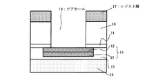
図5乃至図7は、イメージセンサチップに適用可能な従来例に係るBGA型の半導体装置及びその製造方法を示す断面図である。最初に、図5に示すように、半導体基板30上の表面に、絶縁膜、例えば酸化膜31を介してアルミニウム層またはアルミニウム合金層から成るパッド電極層34を形成する。そしてパッド電極層34を含む半導体基板30の表面に、樹脂層35を介して例えばガラスから成る支持基板36を接着する。
5 to 7 are cross-sectional views showing a conventional BGA type semiconductor device applicable to an image sensor chip and a method for manufacturing the same. First, as shown in FIG. 5, a
次に、図6に示すように、パッド電極層34に対応する半導体基板30の裏面に開口部を有したレジスト層37を形成し、これをマスクとして、ドライエッチングを半導体基板30に対して行い、半導体基板30の裏面からパッド電極層34に到達するビアホール38を形成する。ここで、上記エッチングにより形成したビアホール38底部のパッド電極層34の一部上には、エッチングの際に生成されるアルミニウム酸化物50(例えばAl2O3化合物)が形成される。
Next, as illustrated in FIG. 6, a resist layer 37 having an opening is formed on the back surface of the
そして、図7に示すように、ビアホール38内を含む半導体基板30の裏面にバリア層39を形成する。さらに、バリア層39上にメッキ用のシード層40を形成し、そのシード層40上でメッキ処理を行って、例えば銅(Cu)から成る再配線層41を形成する。さらに、再配線層41上に保護層(図示せず)を形成し、保護層の所定位置に開口を設けて再配線層41とコンタクトするボール状端子42を形成する。
Then, as shown in FIG. 7, a barrier layer 39 is formed on the back surface of the
その後、図示しないが、半導体基板及びそれに積層された上記各層を切断して、個々の半導体チップに分離する。こうして、パッド電極層34とボール状端子42とが電気的に接続されたBGA型の半導体装置が形成される。
しかしながら、上記エッチングによりビアホール38を形成した際に、その底部に形成されたアルミニウム酸化物50は、パッド電極層34の一部上に形成されるため、パッド電極層34と再配線層41との間の抵抗を高抵抗に至らしめていた。また、アルミニウム酸化物50は、再配線層41に対するパッド電極層34の被覆性を劣化させるため、再配線層41に断線等の損傷を生じ易くさせていた。従って、半導体装置の特性が劣化するという問題が生じていた。
However, when the
そこで、このアルミニウム酸化物50を再度エッチング等により除去することが考えられるが、この場合、エッチング工程が増すことにより製造プロセスが煩雑になるという問題が生じていた。
Therefore, it is conceivable to remove the
そこで、本発明は、エッチング工程を増加させることなく、電気的特性の劣化を極力抑止し得る半導体装置及びその製造方法を提供するものである。 Therefore, the present invention provides a semiconductor device and a method for manufacturing the same that can suppress deterioration of electrical characteristics as much as possible without increasing the number of etching steps.
本発明の半導体装置は、上記課題に鑑みて為されたものであり、半導体チップの表面に形成され、かつ、第1のバリア層とアルミニウム層又はアルミニウム合金層が積層されて成るパッド電極層と、半導体チップの表面に接着された支持基板と、半導体チップの裏面から第1のバリア層に到達するビアホールと、ビアホール内を含む半導体チップの裏面に形成され、かつ第1のバリア層と接続された再配線層と、を有することを特徴とする。 The semiconductor device of the present invention has been made in view of the above problems, and is formed on the surface of a semiconductor chip, and a pad electrode layer formed by laminating a first barrier layer and an aluminum layer or an aluminum alloy layer. A support substrate bonded to the front surface of the semiconductor chip, a via hole reaching the first barrier layer from the back surface of the semiconductor chip, and formed on the back surface of the semiconductor chip including the inside of the via hole, and connected to the first barrier layer. And a rewiring layer.
また、本発明の半導体装置は、上記構成に加えて、再配線層は、ビアホール内を完全に、もしくは不完全に埋め込むようにして形成されていることを特徴とする。 In addition to the above structure, the semiconductor device of the present invention is characterized in that the rewiring layer is formed so as to completely or incompletely fill the via hole.
また、本発明の半導体装置は、上記再配線層は、メッキ処理またはスパッタ処理により形成されている。 In the semiconductor device of the present invention, the rewiring layer is formed by plating or sputtering.
また、本発明の半導体装置は、再配線層上に導電端子が形成されていることを特徴とする。 The semiconductor device of the present invention is characterized in that a conductive terminal is formed on the rewiring layer.
また、本発明の半導体装置は、ビアホール内を含む半導体チップの裏面と再配線層との間に、第2のバリア層が形成されていることを特徴とする。 The semiconductor device of the present invention is characterized in that a second barrier layer is formed between the back surface of the semiconductor chip including the inside of the via hole and the redistribution layer.
また、本発明の半導体装置の製造方法は、第1のバリア層とアルミニウム層又はアルミニウム合金層が積層されて成るパッド電極層を有する半導体基板を準備し、半導体基板の表面に支持基板を接着する工程と、半導体基板に当該半導体基板の裏面から第1のバリア層に到達するビアホールを形成する工程と、ビアホール内を含む半導体基板の裏面に、第1のバリア層と接続する再配線層を形成する工程と、を有することを特徴とする。 According to the method of manufacturing a semiconductor device of the present invention, a semiconductor substrate having a pad electrode layer formed by laminating a first barrier layer and an aluminum layer or an aluminum alloy layer is prepared, and a support substrate is bonded to the surface of the semiconductor substrate. Forming a via hole reaching the first barrier layer from the back surface of the semiconductor substrate, and forming a rewiring layer connected to the first barrier layer on the back surface of the semiconductor substrate including the inside of the via hole; And a step of performing.
また、本発明の半導体装置の製造方法は、上記再配線層を形成する工程において、再配線層は、ビアホール内を完全に、もしくは不完全に埋め込むようにして形成されることを特徴とする。 The method for manufacturing a semiconductor device according to the present invention is characterized in that, in the step of forming the rewiring layer, the rewiring layer is formed so as to completely or incompletely fill the via hole.
また、本発明の半導体装置の製造方法は、再配線層を形成する工程において、前記再配線層はメッキ処理またはスパッタ処理により形成されることを特徴とする。 The method for manufacturing a semiconductor device according to the present invention is characterized in that, in the step of forming the rewiring layer, the rewiring layer is formed by plating or sputtering.
また、本発明の半導体装置の製造方法は、上記工程に加え、再配線層上に導電端子を形成する工程を含むことを特徴とする。 In addition to the above steps, the method for manufacturing a semiconductor device of the present invention includes a step of forming a conductive terminal on the rewiring layer.
また、本発明の半導体装置の製造方法は、上記工程に加え、ビアホール内を含む半導体基板の裏面と再配線層との間に、第2のバリア層を形成する工程を含むことを特徴とする。 In addition to the above steps, the method for manufacturing a semiconductor device of the present invention includes a step of forming a second barrier layer between the back surface of the semiconductor substrate including the inside of the via hole and the rewiring layer. .
本発明の半導体装置及びその製造方法によれば、アルミニウム層又はアルミニウム合金層と第1のバリア層を積層することにより、パッド電極層を形成した。これにより、エッチングによりビアホールを形成する際に、従来のようなビアホールの底部に位置するパッド電極層上に、アルミニウム酸化物が形成されることが回避される。従って、パッド電極層と再配線層との間が高抵抗となることがなくなり、再配線層に断線等の損傷の発生を極力抑止することができる。その結果、上記ビアホールの形成による半導体装置の電気的特性の劣化を極力抑止することが可能となる。また、アルミニウム酸化物を除去するためのエッチング工程が必要なくなる。 According to the semiconductor device and the manufacturing method thereof of the present invention, the pad electrode layer is formed by laminating the aluminum layer or the aluminum alloy layer and the first barrier layer. This avoids the formation of aluminum oxide on the pad electrode layer located at the bottom of the via hole as in the prior art when the via hole is formed by etching. Therefore, the resistance between the pad electrode layer and the rewiring layer is not increased, and the occurrence of damage such as disconnection in the rewiring layer can be suppressed as much as possible. As a result, it is possible to suppress the deterioration of the electrical characteristics of the semiconductor device due to the formation of the via hole as much as possible. Further, an etching process for removing the aluminum oxide is not necessary.
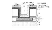
次に、本実施形態に係る半導体装置の構造について、図面を参照して説明する。図4は、本実施形態に係る半導体装置のうち、後述するパッド電極層が存在する領域の断面を示しており、個々の半導体チップに分離する以前の状態を示している。 Next, the structure of the semiconductor device according to the present embodiment will be described with reference to the drawings. FIG. 4 shows a cross section of a region where a later-described pad electrode layer is present in the semiconductor device according to the present embodiment, and shows a state before separation into individual semiconductor chips.
図4に示すように、Siから成る半導体基板10(後に分離されて個々の半導体チップとなる)の表面上に、絶縁膜、例えば酸化膜11を介して第1のバリア層12上にアルミニウム層13(もしくはアルミニウム合金層)が積層されて成るパッド電極層14が形成されている。即ち、第1のバリア層12は、半導体チップ10に近い方の層として形成されている。
As shown in FIG. 4, an aluminum layer is formed on the surface of the
なお、半導体基板10には、不図示の回路が形成されており、パッド電極層14は、上記回路と電気的に接続されている。上記不図示の回路は、例えばCCD(Charge Coupled Device)イメージセンサとして形成されている。この場合、CCDイメージ(画像)の基準点となるオプティカル・ブラック領域が必要となるため、パッド電極層14を構成するアルミニウム層13は、光(赤外線)を遮光し得るピュア・アルミニウムから成ることが好ましく、Al−Cu層でも良い。もしくは、赤外線を透過するするシリコン(Si)を含む合金(例えばAl―Si,Al―Si−Cu等)以外の金属であることが好ましい。
Note that a circuit (not shown) is formed on the
また、第1のバリア層12は、例えばチタンナイトライド(TiN)層であることが好ましい。もしくは、第1のバリア層12は、高融点金属層やその化合物層であれば、チタンナイトライド層以外の金属から成るものであっても良く、タンタル(Ta)層、チタンタングステン(TiW)層、タンタルナイトライド(TaN)層等でも良い。
The
さらに、半導体基板10の表面上に、樹脂層15(接着剤として機能する)を介して、例えば所定の波長帯の光を透過し得るガラスから成る支持基板16が接着されている。そして、半導体基板10のうち、パッド電極層14が存在する領域には、半導体基板10の裏面から、パッド電極層14の第1のバリア層12に到達するビアホール18が形成されている。そして、このビアホール18内を含む半導体基板10の裏面上に、ビアホール18から露出する半導体基板10の側壁を絶縁するために形成した絶縁層を介してそれらを覆うようにして、第2のバリア層19が形成されている。この第2のバリア層19は、例えばチタンナイトライド層であることが好ましい。もしくは、第2のバリア層19は、第1のバリア層と同様にチタンナイトライド層以外の金属から成るものであってもよい。
Further, a
そして、第2のバリア層19上には、メッキ用のシード層20と、メッキ処理により成膜された再配線層21が形成されている。さらに、再線層21上に保護層(図示せず)を形成し、保護層の所定位置に開口を設けて再配線21とコンタクトするボール状端子22が形成されている。即ち、このボール状端子22は、再配線層21、シード層20、第2のバリア層19を介して、パッド電極層14と電気的に接続されている。
On the second barrier layer 19, a seed layer 20 for plating and a rewiring layer 21 formed by plating are formed. Further, a protective layer (not shown) is formed on the rewire layer 21, and a ball-shaped terminal 22 is formed in contact with the rewiring 21 by providing an opening at a predetermined position of the protective layer. That is, the ball-shaped terminal 22 is electrically connected to the
次に、上述した本実施形態に係る半導体装置の製造方法について、図面を参照して説明する。図1乃至図4は、本実施形態に係る半導体装置の製造方法を示す断面図である。図1乃至図4は、パッド電極層14が存在する領域の断面を示しており、個々の半導体チップに分離する以前の状態を示している。
Next, a method for manufacturing the semiconductor device according to this embodiment described above will be described with reference to the drawings. 1 to 4 are cross-sectional views showing a method for manufacturing a semiconductor device according to this embodiment. 1 to 4 show a cross section of a region where the
最初に、図1に示すように、不図示の回路が形成された半導体基板10(後に分離されて個々の半導体チップとなる)の表面上に、絶縁層、例えば酸化膜11を介して、第1のバリア層12上にアルミニウム層13もしくはアルミニウム合金層が積層されて成るパッド電極層14が形成される。即ち、第1のバリア層12は、半導体チップ10に近い方の層として形成される。
First, as shown in FIG. 1, on the surface of a
ここで、上記不図示の回路が、例えばCCDイメージセンサである場合、パッド電極層14を構成するアルミニウム層13は、ピュア・アルミニウムから成ることが好ましい。そして、アルミニウム層13は、光(赤外線)を遮光し得るような厚さ(例えば2μm)で形成されることが好ましい。また、第1のバリア層12は、例えばチタンナイトライド(TiN)層であることが好ましく、本実施形態では250℃の設定温度のスパッタ装置を用いてチタンナイトライド(TiN)層をスパッタ形成している。もしくは、第1のバリア層12は、前述したように高融点金属やその化合物であれば、チタンナイトライド以外の金属から成るものであってもよい。
Here, when the circuit (not shown) is, for example, a CCD image sensor, the
そして、半導体基板10の表面上に、樹脂層15(接着剤として機能する)を介して、例えばガラスから成る支持基板16が接着される。
Then, a
次に、図2に示すように、半導体基板10の裏面上において、パッド電極層14が存在する位置の一部上を開口するレジスト層17を形成する。そして、レジスト層17をマスクとして半導体基板10に対してエッチングを行うことにより、半導体基板10の裏面から、パッド電極層14の第1のバリア層12に到達するビアホール18が形成される。その際のエッチングは、半導体基板10がシリコン(Si)から成る場合、例えばSF6もしくはO2もしくはC4F8等を含むエッチングガスを用いてドライエッチングにより行われることが好ましい。
Next, as shown in FIG. 2, a resist layer 17 is formed on the back surface of the
ここで、ビアホール18の底部に位置するパッド電極層14の面は第1のバリア層12となっているため、上記エッチングはアルミニウム層13にまで及ばない。従って、従来例の半導体装置を示す図6にみられたようなアルミニウム酸化物50(例えばAl2O3化合物)などの酸化物が形成されることはない。
Here, since the surface of the
次に、レジスト層17を除去した後、図3に示すように、ビアホール18内を含む半導体基板10の裏面上に、それらを覆うようにして酸化膜等から成る絶縁層を形成し、第1のバリア層12上の絶縁層を除去した後に、全面に第2のバリア層19が形成される。この第2のバリア層19は、例えばチタンナイトライド層であることが好ましく、本実施形態では200℃以下のCVD装置内でCVD法でチタンナイトライド層を形成している。もしくは、前述したように第2のバリア層19は、高融点金属やその化合物であれば、チタンナイトライド層以外の金属から成るものであってもよい。なお、第2のバリア層19の形成前もしくは形成後に、半導体基板10もしくは第2のバリア層19上に、ボール状端子22に加わる力を緩和するための不図示の緩衝部材を形成してもよい。ここで、第1のバリア層12上の絶縁層(例えば酸化膜)をエッチング除去する際に第1のバリア層12によりアルミニウム層13は露出しないため、アルミニウム酸化物は形成されない。
Next, after removing the resist layer 17, as shown in FIG. 3, an insulating layer made of an oxide film or the like is formed on the back surface of the
次に、図4に示すように、第2のバリア層19上の全面に再配線層21が形成される。その際、まず、第2のバリア層19上の全面に、例えば銅(Cu)から成るメッキ用のシード層20を電界メッキにより形成し、その後、そのシード層20に対して無電界メッキ処理を行うことで、例えば銅(Cu)から成る再配線層21を形成する。ここで、再配線層21は、ビアホール18内を不完全に埋め込むようにして形成される。もしくは、再配線層21は、ビアホール18内を完全に埋め込むように形成されてもよい。
Next, as shown in FIG. 4, a rewiring layer 21 is formed on the entire surface of the second barrier layer 19. At that time, first, a plating seed layer 20 made of, for example, copper (Cu) is formed on the entire surface of the second barrier layer 19 by electroplating, and then the seed layer 20 is subjected to electroless plating. By doing so, the rewiring layer 21 made of, for example, copper (Cu) is formed. Here, the rewiring layer 21 is formed so as to be embedded in the via
さらに、再配線層21上に保護層(図示せず)を形成し、保護層の所定位置に開口を設けた後にスクリーン印刷法によりハンダを印刷してリフローさせることで、前記開口上にボール状端子22を形成する。そして、図示しないが、ダイシングラインに沿って、半導体基板10及びそれに積層された各層を切断することにより、個々の半導体チップ、即ち本実施形態の半導体装置が完成される。
Further, a protective layer (not shown) is formed on the rewiring layer 21, and an opening is provided at a predetermined position of the protective layer, and then solder is printed by screen printing and reflowed to form a ball shape on the opening. Terminal 22 is formed. Although not shown, by cutting the
上述したように、本発明の半導体装置及びその製造方法によれば、半導体基板10の表面に、第1のバリア層12(例えばチタンナイトライド層から成る)上にアルミニウム層13もしくはアルミニウム合金層が積層されて成るパッド電極層14を形成した。
As described above, according to the semiconductor device and the manufacturing method thereof of the present invention, the
これにより、エッチングによりビアホール18を形成する際に、第1のバリア層12の存在によりビアホール18の底部に位置するパッド電極層14上に、アルミニウム酸化物が形成されることが回避される。従って、パッド電極層14と再配線層21との間が高抵抗となることが極力回避される。また、再配線層21に断線等の損傷の発生を極力抑止することができる。その結果、上記ビアホール18の形成による半導体装置の特性の劣化を極力抑止することが可能となる。また、アルミニウム酸化物50を除去する必要がなくなるため、エッチング工程を増やす必要がなくなる。
Thus, when the via
なお、本実施形態では、ビアホール18を含む半導体基板10の裏面に第2のバリア層19を形成したが、本発明はこれに制限されるものではない。即ち、本発明は、ビアホール18を含む半導体基板10の裏面に、第2のバリア層19が形成されずに、前記絶縁層を介して再配線層21が形成されるものであってもよい。
In the present embodiment, the second barrier layer 19 is formed on the back surface of the
また、本実施形態では、再配線層21は、メッキ処理により形成されるものとしたが、本発明はこれに制限されるものではない。即ち、本発明は、メッキ用のシード層20は形成されず、メッキ処理以外の方法により再配線層21が形成されるものであってもよく、例えばアルミニウム(Al)等の金属をスパッタ形成するものでも良い。 In the present embodiment, the rewiring layer 21 is formed by plating, but the present invention is not limited to this. That is, in the present invention, the seed layer 20 for plating may not be formed, and the rewiring layer 21 may be formed by a method other than plating. For example, a metal such as aluminum (Al) is formed by sputtering. Things can be used.
また、本発明は、ボール状端子22が形成された半導体装置に適用されるものとしたが、本発明はこれに制限されるものではない。即ち、本発明は、半導体基板を貫通するビアホールが形成されて成るものであれば、ボール状端子が形成されない半導体装置にも適用されるものである。例えば、LGA(Land Grid Array)型の半導体装置にも適用される。 Moreover, although the present invention is applied to a semiconductor device in which the ball-shaped terminals 22 are formed, the present invention is not limited to this. That is, the present invention can be applied to a semiconductor device in which a ball terminal is not formed as long as a via hole penetrating a semiconductor substrate is formed. For example, the present invention is also applied to an LGA (Land Grid Array) type semiconductor device.
更に言えば、本発明ではビアホール18を形成する側のアルミニウム層13上に第1のバリア層12を形成しているため、ビアホール開口時のエッチング処理時にアルミニウム層13の表面がオーバーエッチングによりエッチングされることが抑制される。従って、オーバーエッチングにより削られてしまう量を考慮してアルミニウム層13の膜厚を多くする必要がなくなる。
Furthermore, in the present invention, since the
Claims (16)
前記半導体チップの表面に接着された支持基板と、
前記半導体チップの裏面から前記第1のバリア層に到達するビアホールと、
前記ビアホール内を含む前記半導体チップの裏面に形成され、かつ前記第1のバリア層と接続された再配線層と、
を有することを特徴とする半導体装置。 A pad electrode layer formed on the surface of the semiconductor chip and formed by laminating a first barrier layer and an aluminum layer or an aluminum alloy layer;
A support substrate bonded to the surface of the semiconductor chip;
A via hole reaching the first barrier layer from the back surface of the semiconductor chip;
A redistribution layer formed on the back surface of the semiconductor chip including in the via hole and connected to the first barrier layer;
A semiconductor device comprising:
前記半導体基板の表面に支持基板を接着する工程と、
前記半導体基板に、当該半導体基板の裏面から前記第1のバリア層に到達するビアホールを形成する工程と、
前記ビアホール内を含む前記半導体基板の裏面に、前記第1のバリア層と接続する再配線層を形成する工程と、
を有することを特徴とする半導体装置の製造方法。 Preparing a semiconductor substrate having a pad electrode layer formed by laminating a first barrier layer and an aluminum layer or an aluminum alloy layer;
Bonding a support substrate to the surface of the semiconductor substrate;
Forming a via hole in the semiconductor substrate reaching the first barrier layer from the back surface of the semiconductor substrate;
Forming a redistribution layer connected to the first barrier layer on the back surface of the semiconductor substrate including the inside of the via hole;
A method for manufacturing a semiconductor device, comprising:
Priority Applications (7)
| Application Number | Priority Date | Filing Date | Title |
|---|---|---|---|
| JP2004040409A JP2005235860A (en) | 2004-02-17 | 2004-02-17 | Semiconductor device and manufacturing method thereof |
| TW094102436A TWI261343B (en) | 2004-02-17 | 2005-01-27 | Semiconductor device and method of manufacturing the same |
| US11/054,603 US7256497B2 (en) | 2004-02-17 | 2005-02-10 | Semiconductor device with a barrier layer and a metal layer |
| KR1020050012334A KR100646722B1 (en) | 2004-02-17 | 2005-02-15 | Semiconductor device and manufacturing method thereof |
| EP05003396.8A EP1564806B1 (en) | 2004-02-17 | 2005-02-17 | Semiconductor device and manufacturing method of the same |
| CN2005100093505A CN1658385A (en) | 2004-02-17 | 2005-02-17 | Semiconductor device and manufacturing method of the same |
| US11/822,262 US7759247B2 (en) | 2004-02-17 | 2007-07-03 | Manufacturing method of semiconductor device with a barrier layer and a metal layer |
Applications Claiming Priority (1)
| Application Number | Priority Date | Filing Date | Title |
|---|---|---|---|
| JP2004040409A JP2005235860A (en) | 2004-02-17 | 2004-02-17 | Semiconductor device and manufacturing method thereof |
Publications (2)
| Publication Number | Publication Date |
|---|---|
| JP2005235860A true JP2005235860A (en) | 2005-09-02 |
| JP2005235860A5 JP2005235860A5 (en) | 2007-03-15 |
Family
ID=34697999
Family Applications (1)
| Application Number | Title | Priority Date | Filing Date |
|---|---|---|---|
| JP2004040409A Pending JP2005235860A (en) | 2004-02-17 | 2004-02-17 | Semiconductor device and manufacturing method thereof |
Country Status (6)
| Country | Link |
|---|---|
| US (2) | US7256497B2 (en) |
| EP (1) | EP1564806B1 (en) |
| JP (1) | JP2005235860A (en) |
| KR (1) | KR100646722B1 (en) |
| CN (1) | CN1658385A (en) |
| TW (1) | TWI261343B (en) |
Cited By (6)
| Publication number | Priority date | Publication date | Assignee | Title |
|---|---|---|---|---|
| JP2009194399A (en) * | 2009-05-27 | 2009-08-27 | Sony Corp | Solid-state imaging device |
| WO2011058712A1 (en) | 2009-11-12 | 2011-05-19 | パナソニック株式会社 | Semiconductor device and method for manufacturing semiconductor device |
| WO2012057200A1 (en) * | 2010-10-29 | 2012-05-03 | 株式会社フジクラ | Process for manufacture of through-type wiring substrate, and through-type wiring substrate |
| JP2013247254A (en) * | 2012-05-25 | 2013-12-09 | Lapis Semiconductor Co Ltd | Semiconductor device and manufacturing method of the same |
| US9349673B2 (en) | 2012-07-04 | 2016-05-24 | Seiko Epson Corporation | Substrate, method of manufacturing substrate, semiconductor device, and electronic apparatus |
| JP2016115837A (en) * | 2014-12-16 | 2016-06-23 | シチズンホールディングス株式会社 | Semiconductor device and method of manufacturing the same |
Families Citing this family (19)
| Publication number | Priority date | Publication date | Assignee | Title |
|---|---|---|---|---|
| JP4850392B2 (en) | 2004-02-17 | 2012-01-11 | 三洋電機株式会社 | Manufacturing method of semiconductor device |
| TWI250596B (en) * | 2004-07-23 | 2006-03-01 | Ind Tech Res Inst | Wafer-level chip scale packaging method |
| JP4443379B2 (en) | 2004-10-26 | 2010-03-31 | 三洋電機株式会社 | Manufacturing method of semiconductor device |
| JP4873517B2 (en) | 2004-10-28 | 2012-02-08 | オンセミコンダクター・トレーディング・リミテッド | Semiconductor device and manufacturing method thereof |
| JP4641820B2 (en) * | 2005-02-17 | 2011-03-02 | 三洋電機株式会社 | Manufacturing method of semiconductor device |
| US7485967B2 (en) | 2005-03-10 | 2009-02-03 | Sanyo Electric Co., Ltd. | Semiconductor device with via hole for electric connection |
| US9601474B2 (en) * | 2005-07-22 | 2017-03-21 | Invensas Corporation | Electrically stackable semiconductor wafer and chip packages |
| JP2007184553A (en) | 2005-12-06 | 2007-07-19 | Sanyo Electric Co Ltd | Semiconductor device and its fabrication process |
| JP2007311771A (en) * | 2006-04-21 | 2007-11-29 | Sanyo Electric Co Ltd | Semiconductor device and method of manufacturing the same |
| JP4812512B2 (en) * | 2006-05-19 | 2011-11-09 | オンセミコンダクター・トレーディング・リミテッド | Manufacturing method of semiconductor device |
| JP5143382B2 (en) * | 2006-07-27 | 2013-02-13 | オンセミコンダクター・トレーディング・リミテッド | Semiconductor device and manufacturing method thereof |
| US7927966B2 (en) * | 2006-12-12 | 2011-04-19 | Nxp B.V. | Method of manufacturing openings in a substrate, a via in substrate, and a semiconductor device comprising such a via |
| US20090089515A1 (en) * | 2007-10-02 | 2009-04-02 | Qualcomm Incorporated | Memory Controller for Performing Memory Block Initialization and Copy |
| JP5150566B2 (en) * | 2009-06-22 | 2013-02-20 | 株式会社東芝 | Semiconductor device and camera module |
| JP5955706B2 (en) * | 2012-08-29 | 2016-07-20 | ルネサスエレクトロニクス株式会社 | Semiconductor device and manufacturing method thereof |
| US20140151095A1 (en) * | 2012-12-05 | 2014-06-05 | Samsung Electro-Mechanics Co., Ltd. | Printed circuit board and method for manufacturing the same |
| US9466554B2 (en) * | 2014-02-13 | 2016-10-11 | Qualcomm Incorporated | Integrated device comprising via with side barrier layer traversing encapsulation layer |
| CN106935561B (en) * | 2015-12-30 | 2019-10-18 | 力成科技股份有限公司 | Prevent the semiconductor packaging structure that via hole is electrically broken |
| US11609207B2 (en) | 2020-03-31 | 2023-03-21 | Analog Devices International Unlimited Company | Electrochemical sensor and method of forming thereof |
Citations (7)
| Publication number | Priority date | Publication date | Assignee | Title |
|---|---|---|---|---|
| JP2001189414A (en) * | 1999-12-27 | 2001-07-10 | Seiko Epson Corp | Semiconductor chip, manufacturing method therefor, semiconductor module, and electronic apparatus |
| JP2002083936A (en) * | 2000-09-08 | 2002-03-22 | Fujitsu Quantum Devices Ltd | Chemical compound semiconductor device |
| JP2003203889A (en) * | 2002-01-08 | 2003-07-18 | Fujitsu Ltd | Method for manufacturing semiconductor device |
| JP2003309221A (en) * | 2002-04-15 | 2003-10-31 | Sanyo Electric Co Ltd | Method of manufacturing semiconductor device |
| JP2003328180A (en) * | 2002-05-17 | 2003-11-19 | Denso Corp | Method of filling plating into bottomed hole |
| JP2003332417A (en) * | 2002-05-08 | 2003-11-21 | Toshiba Corp | Method for manufacturing semiconductor chip |
| JP2004004663A (en) * | 2002-03-26 | 2004-01-08 | Semiconductor Energy Lab Co Ltd | Light emitting device, liquid crystal display device, and method of manufacturing them |
Family Cites Families (54)
| Publication number | Priority date | Publication date | Assignee | Title |
|---|---|---|---|---|
| FR2553579B1 (en) * | 1983-10-12 | 1985-12-27 | Commissariat Energie Atomique | METHOD FOR MANUFACTURING A THIN FILM TRANSISTOR WITH SELF-ALIGNED GRID |
| US4560436A (en) * | 1984-07-02 | 1985-12-24 | Motorola, Inc. | Process for etching tapered polyimide vias |
| US4678542A (en) * | 1986-07-25 | 1987-07-07 | Energy Conversion Devices, Inc. | Self-alignment process for thin film diode array fabrication |
| US4827326A (en) * | 1987-11-02 | 1989-05-02 | Motorola, Inc. | Integrated circuit having polyimide/metal passivation layer and method of manufacture using metal lift-off |
| US5173753A (en) * | 1989-08-10 | 1992-12-22 | Industrial Technology Research Institute | Inverted coplanar amorphous silicon thin film transistor which provides small contact capacitance and resistance |
| US5300813A (en) * | 1992-02-26 | 1994-04-05 | International Business Machines Corporation | Refractory metal capped low resistivity metal conductor lines and vias |
| US5242864A (en) * | 1992-06-05 | 1993-09-07 | Intel Corporation | Polyimide process for protecting integrated circuits |
| US6028348A (en) | 1993-11-30 | 2000-02-22 | Texas Instruments Incorporated | Low thermal impedance integrated circuit |
| US5554564A (en) * | 1994-08-01 | 1996-09-10 | Texas Instruments Incorporated | Pre-oxidizing high-dielectric-constant material electrodes |
| US5567657A (en) * | 1995-12-04 | 1996-10-22 | General Electric Company | Fabrication and structures of two-sided molded circuit modules with flexible interconnect layers |
| US6111317A (en) * | 1996-01-18 | 2000-08-29 | Kabushiki Kaisha Toshiba | Flip-chip connection type semiconductor integrated circuit device |
| US5682065A (en) * | 1996-03-12 | 1997-10-28 | Micron Technology, Inc. | Hermetic chip and method of manufacture |
| JP3287392B2 (en) * | 1997-08-22 | 2002-06-04 | 日本電気株式会社 | Semiconductor device and manufacturing method thereof |
| JPH11111753A (en) * | 1997-10-01 | 1999-04-23 | Mitsubishi Electric Corp | Semiconductor device |
| JP3033564B2 (en) * | 1997-10-02 | 2000-04-17 | セイコーエプソン株式会社 | Method for manufacturing semiconductor device |
| US6054768A (en) * | 1997-10-02 | 2000-04-25 | Micron Technology, Inc. | Metal fill by treatment of mobility layers |
| TWI224221B (en) * | 1998-01-30 | 2004-11-21 | Seiko Epson Corp | Electro-optic apparatus, electronic apparatus using the same, and its manufacturing method |
| IL123207A0 (en) | 1998-02-06 | 1998-09-24 | Shellcase Ltd | Integrated circuit device |
| US6287977B1 (en) * | 1998-07-31 | 2001-09-11 | Applied Materials, Inc. | Method and apparatus for forming improved metal interconnects |
| US6479900B1 (en) * | 1998-12-22 | 2002-11-12 | Sanyo Electric Co., Ltd. | Semiconductor device and method of manufacturing the same |
| US6154366A (en) * | 1999-11-23 | 2000-11-28 | Intel Corporation | Structures and processes for fabricating moisture resistant chip-on-flex packages |
| JP3907151B2 (en) * | 2000-01-25 | 2007-04-18 | 株式会社東芝 | Manufacturing method of semiconductor device |
| US6475889B1 (en) | 2000-04-11 | 2002-11-05 | Cree, Inc. | Method of forming vias in silicon carbide and resulting devices and circuits |
| JP2002076293A (en) * | 2000-09-01 | 2002-03-15 | Matsushita Electric Ind Co Ltd | Method for manufacturing capacitor and semiconductor device |
| JP4183375B2 (en) * | 2000-10-04 | 2008-11-19 | 沖電気工業株式会社 | Semiconductor device and manufacturing method thereof |
| US6423570B1 (en) * | 2000-10-18 | 2002-07-23 | Intel Corporation | Method to protect an encapsulated die package during back grinding with a solder metallization layer and devices formed thereby |
| US6555906B2 (en) * | 2000-12-15 | 2003-04-29 | Intel Corporation | Microelectronic package having a bumpless laminated interconnection layer |
| US20020123228A1 (en) | 2001-03-02 | 2002-09-05 | Smoak Richard C. | Method to improve the reliability of gold to aluminum wire bonds with small pad openings |
| JP2002319669A (en) * | 2001-04-23 | 2002-10-31 | Hamamatsu Photonics Kk | Backside incident type photodiode and photodiode array |
| JP2002329722A (en) * | 2001-04-27 | 2002-11-15 | Nec Corp | Semiconductor device and its manufacturing method |
| JP2003031575A (en) * | 2001-07-17 | 2003-01-31 | Nec Corp | Semiconductor device and manufacturing method therefor |
| JP4309608B2 (en) * | 2001-09-12 | 2009-08-05 | 株式会社東芝 | Semiconductor device and manufacturing method thereof |
| JP3825314B2 (en) * | 2001-12-17 | 2006-09-27 | 株式会社ルネサステクノロジ | Manufacturing method of semiconductor device |
| TWI232560B (en) * | 2002-04-23 | 2005-05-11 | Sanyo Electric Co | Semiconductor device and its manufacture |
| TWI229435B (en) | 2002-06-18 | 2005-03-11 | Sanyo Electric Co | Manufacture of semiconductor device |
| JP2004040059A (en) * | 2002-07-08 | 2004-02-05 | Fujitsu Ltd | Manufacturing method of semiconductor memory device, and semiconductor memory device |
| US6902872B2 (en) * | 2002-07-29 | 2005-06-07 | Hewlett-Packard Development Company, L.P. | Method of forming a through-substrate interconnect |
| TWI227050B (en) | 2002-10-11 | 2005-01-21 | Sanyo Electric Co | Semiconductor device and method for manufacturing the same |
| JP4511148B2 (en) | 2002-10-11 | 2010-07-28 | 三洋電機株式会社 | Manufacturing method of semiconductor device |
| JP2004207327A (en) * | 2002-12-24 | 2004-07-22 | Renesas Technology Corp | Semiconductor device and its manufacturing method |
| JP4290421B2 (en) * | 2002-12-27 | 2009-07-08 | Necエレクトロニクス株式会社 | Semiconductor device and manufacturing method thereof |
| JP4130158B2 (en) | 2003-06-09 | 2008-08-06 | 三洋電機株式会社 | Semiconductor device manufacturing method, semiconductor device |
| JP3970211B2 (en) | 2003-06-24 | 2007-09-05 | 三洋電機株式会社 | Semiconductor device and manufacturing method thereof |
| JP4499386B2 (en) * | 2003-07-29 | 2010-07-07 | 浜松ホトニクス株式会社 | Manufacturing method of back-illuminated photodetector |
| US20050126420A1 (en) | 2003-09-10 | 2005-06-16 | Givens Richard W. | Wall breaching apparatus and method |
| JP4011002B2 (en) * | 2003-09-11 | 2007-11-21 | シャープ株式会社 | Active substrate, display device and manufacturing method thereof |
| JP4850392B2 (en) * | 2004-02-17 | 2012-01-11 | 三洋電機株式会社 | Manufacturing method of semiconductor device |
| TWI249767B (en) * | 2004-02-17 | 2006-02-21 | Sanyo Electric Co | Method for making a semiconductor device |
| DE102004015862B4 (en) * | 2004-03-31 | 2006-11-16 | Advanced Micro Devices, Inc., Sunnyvale | A method of forming a conductive barrier layer in critical openings by means of a final deposition step after backsputter deposition |
| KR100592388B1 (en) * | 2004-04-01 | 2006-06-22 | 엘지전자 주식회사 | Organic electroluminescent display device and manufacturing method thereof |
| DE102004021261B4 (en) * | 2004-04-30 | 2007-03-22 | Advanced Micro Devices, Inc., Sunnyvale | Semiconductor device having a hybrid metallization layer stack for improved mechanical strength during and after insertion into a package |
| TWI272683B (en) * | 2004-05-24 | 2007-02-01 | Sanyo Electric Co | Semiconductor device and manufacturing method thereof |
| JP4376715B2 (en) * | 2004-07-16 | 2009-12-02 | 三洋電機株式会社 | Manufacturing method of semiconductor device |
| JP4373866B2 (en) * | 2004-07-16 | 2009-11-25 | 三洋電機株式会社 | Manufacturing method of semiconductor device |
-
2004
- 2004-02-17 JP JP2004040409A patent/JP2005235860A/en active Pending
-
2005
- 2005-01-27 TW TW094102436A patent/TWI261343B/en active
- 2005-02-10 US US11/054,603 patent/US7256497B2/en active Active
- 2005-02-15 KR KR1020050012334A patent/KR100646722B1/en active IP Right Grant
- 2005-02-17 EP EP05003396.8A patent/EP1564806B1/en active Active
- 2005-02-17 CN CN2005100093505A patent/CN1658385A/en active Pending
-
2007
- 2007-07-03 US US11/822,262 patent/US7759247B2/en active Active
Patent Citations (7)
| Publication number | Priority date | Publication date | Assignee | Title |
|---|---|---|---|---|
| JP2001189414A (en) * | 1999-12-27 | 2001-07-10 | Seiko Epson Corp | Semiconductor chip, manufacturing method therefor, semiconductor module, and electronic apparatus |
| JP2002083936A (en) * | 2000-09-08 | 2002-03-22 | Fujitsu Quantum Devices Ltd | Chemical compound semiconductor device |
| JP2003203889A (en) * | 2002-01-08 | 2003-07-18 | Fujitsu Ltd | Method for manufacturing semiconductor device |
| JP2004004663A (en) * | 2002-03-26 | 2004-01-08 | Semiconductor Energy Lab Co Ltd | Light emitting device, liquid crystal display device, and method of manufacturing them |
| JP2003309221A (en) * | 2002-04-15 | 2003-10-31 | Sanyo Electric Co Ltd | Method of manufacturing semiconductor device |
| JP2003332417A (en) * | 2002-05-08 | 2003-11-21 | Toshiba Corp | Method for manufacturing semiconductor chip |
| JP2003328180A (en) * | 2002-05-17 | 2003-11-19 | Denso Corp | Method of filling plating into bottomed hole |
Cited By (8)
| Publication number | Priority date | Publication date | Assignee | Title |
|---|---|---|---|---|
| JP2009194399A (en) * | 2009-05-27 | 2009-08-27 | Sony Corp | Solid-state imaging device |
| WO2011058712A1 (en) | 2009-11-12 | 2011-05-19 | パナソニック株式会社 | Semiconductor device and method for manufacturing semiconductor device |
| US8471367B2 (en) | 2009-11-12 | 2013-06-25 | Panasonic Corporation | Semiconductor device and method for manufacturing semiconductor device |
| WO2012057200A1 (en) * | 2010-10-29 | 2012-05-03 | 株式会社フジクラ | Process for manufacture of through-type wiring substrate, and through-type wiring substrate |
| JP2012099548A (en) * | 2010-10-29 | 2012-05-24 | Fujikura Ltd | Method for manufacturing through wiring board and through wiring board |
| JP2013247254A (en) * | 2012-05-25 | 2013-12-09 | Lapis Semiconductor Co Ltd | Semiconductor device and manufacturing method of the same |
| US9349673B2 (en) | 2012-07-04 | 2016-05-24 | Seiko Epson Corporation | Substrate, method of manufacturing substrate, semiconductor device, and electronic apparatus |
| JP2016115837A (en) * | 2014-12-16 | 2016-06-23 | シチズンホールディングス株式会社 | Semiconductor device and method of manufacturing the same |
Also Published As
| Publication number | Publication date |
|---|---|
| CN1658385A (en) | 2005-08-24 |
| TW200529384A (en) | 2005-09-01 |
| KR20060041950A (en) | 2006-05-12 |
| TWI261343B (en) | 2006-09-01 |
| EP1564806B1 (en) | 2016-12-14 |
| KR100646722B1 (en) | 2006-11-23 |
| EP1564806A1 (en) | 2005-08-17 |
| US20070254475A1 (en) | 2007-11-01 |
| US20050269704A1 (en) | 2005-12-08 |
| US7256497B2 (en) | 2007-08-14 |
| US7759247B2 (en) | 2010-07-20 |
Similar Documents
| Publication | Publication Date | Title |
|---|---|---|
| KR100646722B1 (en) | Semiconductor device and manufacturing method thereof | |
| JP4307284B2 (en) | Manufacturing method of semiconductor device | |
| JP4850392B2 (en) | Manufacturing method of semiconductor device | |
| JP4130158B2 (en) | Semiconductor device manufacturing method, semiconductor device | |
| JP4373866B2 (en) | Manufacturing method of semiconductor device | |
| KR100659625B1 (en) | Semiconductor device and method for manufacturing the same | |
| JP2004349593A (en) | Semiconductor device and method for manufacturing the same | |
| JP2005019521A (en) | Method of manufacturing semiconductor device | |
| JP4307296B2 (en) | Manufacturing method of semiconductor device | |
| JP4544902B2 (en) | Semiconductor device and manufacturing method thereof | |
| JP2004153260A (en) | Semiconductor device and method of manufacturing same | |
| JP4282514B2 (en) | Manufacturing method of semiconductor device | |
| JP2006128171A (en) | Semiconductor apparatus and its manufacturing method | |
| JP4845986B2 (en) | Semiconductor device | |
| JP4769926B2 (en) | Semiconductor device and manufacturing method thereof | |
| JP2005277173A (en) | Semiconductor device, and its manufacturing method | |
| JP2010073889A (en) | Semiconductor device and method of manufacturing the same | |
| JP2006049592A (en) | Method of manufacturing semiconductor device | |
| JP2005260080A (en) | Semiconductor device and its manufacturing method |
Legal Events
| Date | Code | Title | Description |
|---|---|---|---|
| A521 | Request for written amendment filed |
Free format text: JAPANESE INTERMEDIATE CODE: A523 Effective date: 20070129 |
|
| A621 | Written request for application examination |
Free format text: JAPANESE INTERMEDIATE CODE: A621 Effective date: 20070129 |
|
| A977 | Report on retrieval |
Free format text: JAPANESE INTERMEDIATE CODE: A971007 Effective date: 20090527 |
|
| A131 | Notification of reasons for refusal |
Free format text: JAPANESE INTERMEDIATE CODE: A131 Effective date: 20101007 |
|
| A521 | Request for written amendment filed |
Free format text: JAPANESE INTERMEDIATE CODE: A523 Effective date: 20101129 |
|
| A02 | Decision of refusal |
Free format text: JAPANESE INTERMEDIATE CODE: A02 Effective date: 20110124 |