JP5025123B2 - Display device and electronic device - Google Patents
Display device and electronic device Download PDFInfo
- Publication number
- JP5025123B2 JP5025123B2 JP2005332454A JP2005332454A JP5025123B2 JP 5025123 B2 JP5025123 B2 JP 5025123B2 JP 2005332454 A JP2005332454 A JP 2005332454A JP 2005332454 A JP2005332454 A JP 2005332454A JP 5025123 B2 JP5025123 B2 JP 5025123B2
- Authority
- JP
- Japan
- Prior art keywords
- light
- electrode
- monitor element
- film
- display device
- Prior art date
- Legal status (The legal status is an assumption and is not a legal conclusion. Google has not performed a legal analysis and makes no representation as to the accuracy of the status listed.)
- Expired - Fee Related
Links
- 239000010408 film Substances 0.000 claims description 223
- 239000010410 layer Substances 0.000 claims description 70
- 239000010409 thin film Substances 0.000 claims description 33
- 239000011229 interlayer Substances 0.000 claims description 27
- 239000011159 matrix material Substances 0.000 claims description 11
- 230000009977 dual effect Effects 0.000 claims description 2
- 238000012544 monitoring process Methods 0.000 claims 3
- 239000000758 substrate Substances 0.000 description 47
- 239000000463 material Substances 0.000 description 41
- 239000004065 semiconductor Substances 0.000 description 37
- 238000000034 method Methods 0.000 description 29
- 229920005989 resin Polymers 0.000 description 18
- 239000011347 resin Substances 0.000 description 18
- 239000002274 desiccant Substances 0.000 description 14
- 238000004519 manufacturing process Methods 0.000 description 14
- 239000003566 sealing material Substances 0.000 description 14
- IJGRMHOSHXDMSA-UHFFFAOYSA-N Atomic nitrogen Chemical compound N#N IJGRMHOSHXDMSA-UHFFFAOYSA-N 0.000 description 13
- 229910052581 Si3N4 Inorganic materials 0.000 description 12
- QVGXLLKOCUKJST-UHFFFAOYSA-N atomic oxygen Chemical compound [O] QVGXLLKOCUKJST-UHFFFAOYSA-N 0.000 description 12
- 230000006870 function Effects 0.000 description 12
- 229910052760 oxygen Inorganic materials 0.000 description 12
- 239000001301 oxygen Substances 0.000 description 12
- 229910052710 silicon Inorganic materials 0.000 description 12
- HQVNEWCFYHHQES-UHFFFAOYSA-N silicon nitride Chemical compound N12[Si]34N5[Si]62N3[Si]51N64 HQVNEWCFYHHQES-UHFFFAOYSA-N 0.000 description 12
- XUIMIQQOPSSXEZ-UHFFFAOYSA-N Silicon Chemical compound [Si] XUIMIQQOPSSXEZ-UHFFFAOYSA-N 0.000 description 11
- 238000005401 electroluminescence Methods 0.000 description 11
- 239000010703 silicon Substances 0.000 description 11
- 239000000565 sealant Substances 0.000 description 10
- VYPSYNLAJGMNEJ-UHFFFAOYSA-N silicon dioxide Inorganic materials O=[Si]=O VYPSYNLAJGMNEJ-UHFFFAOYSA-N 0.000 description 10
- 239000000126 substance Substances 0.000 description 10
- 239000012535 impurity Substances 0.000 description 9
- 239000010936 titanium Substances 0.000 description 9
- 230000006866 deterioration Effects 0.000 description 8
- 239000000945 filler Substances 0.000 description 8
- 238000010438 heat treatment Methods 0.000 description 8
- 230000008569 process Effects 0.000 description 8
- 229910052782 aluminium Inorganic materials 0.000 description 7
- QVQLCTNNEUAWMS-UHFFFAOYSA-N barium oxide Chemical compound [Ba]=O QVQLCTNNEUAWMS-UHFFFAOYSA-N 0.000 description 7
- 230000015572 biosynthetic process Effects 0.000 description 7
- -1 calcium nitride Chemical class 0.000 description 7
- 238000010586 diagram Methods 0.000 description 7
- 238000007789 sealing Methods 0.000 description 7
- 229910052814 silicon oxide Inorganic materials 0.000 description 7
- 229910052719 titanium Inorganic materials 0.000 description 7
- RTAQQCXQSZGOHL-UHFFFAOYSA-N Titanium Chemical compound [Ti] RTAQQCXQSZGOHL-UHFFFAOYSA-N 0.000 description 6
- 239000011521 glass Substances 0.000 description 6
- 229910052757 nitrogen Inorganic materials 0.000 description 6
- 229920001721 polyimide Polymers 0.000 description 6
- 229920001187 thermosetting polymer Polymers 0.000 description 6
- OKTJSMMVPCPJKN-UHFFFAOYSA-N Carbon Chemical compound [C] OKTJSMMVPCPJKN-UHFFFAOYSA-N 0.000 description 5
- 239000004642 Polyimide Substances 0.000 description 5
- 230000004888 barrier function Effects 0.000 description 5
- 229910052799 carbon Inorganic materials 0.000 description 5
- 239000003822 epoxy resin Substances 0.000 description 5
- 239000012212 insulator Substances 0.000 description 5
- 229910052751 metal Inorganic materials 0.000 description 5
- 239000002184 metal Substances 0.000 description 5
- 238000005192 partition Methods 0.000 description 5
- 229920000647 polyepoxide Polymers 0.000 description 5
- 230000001681 protective effect Effects 0.000 description 5
- XLYOFNOQVPJJNP-UHFFFAOYSA-N water Substances O XLYOFNOQVPJJNP-UHFFFAOYSA-N 0.000 description 5
- 229910045601 alloy Inorganic materials 0.000 description 4
- 239000000956 alloy Substances 0.000 description 4
- XAGFODPZIPBFFR-UHFFFAOYSA-N aluminium Chemical compound [Al] XAGFODPZIPBFFR-UHFFFAOYSA-N 0.000 description 4
- 229910052791 calcium Inorganic materials 0.000 description 4
- 239000011575 calcium Substances 0.000 description 4
- 230000008859 change Effects 0.000 description 4
- PMHQVHHXPFUNSP-UHFFFAOYSA-M copper(1+);methylsulfanylmethane;bromide Chemical compound Br[Cu].CSC PMHQVHHXPFUNSP-UHFFFAOYSA-M 0.000 description 4
- 238000002425 crystallisation Methods 0.000 description 4
- 230000007423 decrease Effects 0.000 description 4
- 230000007613 environmental effect Effects 0.000 description 4
- 239000001257 hydrogen Substances 0.000 description 4
- 229910052739 hydrogen Inorganic materials 0.000 description 4
- TWNQGVIAIRXVLR-UHFFFAOYSA-N oxo(oxoalumanyloxy)alumane Chemical compound O=[Al]O[Al]=O TWNQGVIAIRXVLR-UHFFFAOYSA-N 0.000 description 4
- 229920003023 plastic Polymers 0.000 description 4
- 239000004033 plastic Substances 0.000 description 4
- 239000002356 single layer Substances 0.000 description 4
- 238000001179 sorption measurement Methods 0.000 description 4
- UFHFLCQGNIYNRP-UHFFFAOYSA-N Hydrogen Chemical compound [H][H] UFHFLCQGNIYNRP-UHFFFAOYSA-N 0.000 description 3
- PXHVJJICTQNCMI-UHFFFAOYSA-N Nickel Chemical compound [Ni] PXHVJJICTQNCMI-UHFFFAOYSA-N 0.000 description 3
- XLOMVQKBTHCTTD-UHFFFAOYSA-N Zinc monoxide Chemical compound [Zn]=O XLOMVQKBTHCTTD-UHFFFAOYSA-N 0.000 description 3
- 239000012298 atmosphere Substances 0.000 description 3
- 239000003990 capacitor Substances 0.000 description 3
- 230000000052 comparative effect Effects 0.000 description 3
- KPUWHANPEXNPJT-UHFFFAOYSA-N disiloxane Chemical class [SiH3]O[SiH3] KPUWHANPEXNPJT-UHFFFAOYSA-N 0.000 description 3
- 238000001704 evaporation Methods 0.000 description 3
- AMGQUBHHOARCQH-UHFFFAOYSA-N indium;oxotin Chemical compound [In].[Sn]=O AMGQUBHHOARCQH-UHFFFAOYSA-N 0.000 description 3
- 239000011261 inert gas Substances 0.000 description 3
- 239000000203 mixture Substances 0.000 description 3
- 150000004767 nitrides Chemical class 0.000 description 3
- 239000012788 optical film Substances 0.000 description 3
- 238000002161 passivation Methods 0.000 description 3
- 230000002093 peripheral effect Effects 0.000 description 3
- 229920000642 polymer Polymers 0.000 description 3
- 229910052709 silver Inorganic materials 0.000 description 3
- 239000004925 Acrylic resin Substances 0.000 description 2
- 229920000178 Acrylic resin Polymers 0.000 description 2
- 229910017073 AlLi Inorganic materials 0.000 description 2
- ZOXJGFHDIHLPTG-UHFFFAOYSA-N Boron Chemical compound [B] ZOXJGFHDIHLPTG-UHFFFAOYSA-N 0.000 description 2
- 229910004261 CaF 2 Inorganic materials 0.000 description 2
- 229910017911 MgIn Inorganic materials 0.000 description 2
- ZOKXTWBITQBERF-UHFFFAOYSA-N Molybdenum Chemical compound [Mo] ZOKXTWBITQBERF-UHFFFAOYSA-N 0.000 description 2
- OAICVXFJPJFONN-UHFFFAOYSA-N Phosphorus Chemical compound [P] OAICVXFJPJFONN-UHFFFAOYSA-N 0.000 description 2
- NRTOMJZYCJJWKI-UHFFFAOYSA-N Titanium nitride Chemical compound [Ti]#N NRTOMJZYCJJWKI-UHFFFAOYSA-N 0.000 description 2
- 229910021536 Zeolite Inorganic materials 0.000 description 2
- 238000010521 absorption reaction Methods 0.000 description 2
- 229910052788 barium Inorganic materials 0.000 description 2
- 229910052796 boron Inorganic materials 0.000 description 2
- DQXBYHZEEUGOBF-UHFFFAOYSA-N but-3-enoic acid;ethene Chemical compound C=C.OC(=O)CC=C DQXBYHZEEUGOBF-UHFFFAOYSA-N 0.000 description 2
- ODINCKMPIJJUCX-UHFFFAOYSA-N calcium oxide Inorganic materials [Ca]=O ODINCKMPIJJUCX-UHFFFAOYSA-N 0.000 description 2
- 239000000919 ceramic Substances 0.000 description 2
- 230000008025 crystallization Effects 0.000 description 2
- HNPSIPDUKPIQMN-UHFFFAOYSA-N dioxosilane;oxo(oxoalumanyloxy)alumane Chemical compound O=[Si]=O.O=[Al]O[Al]=O HNPSIPDUKPIQMN-UHFFFAOYSA-N 0.000 description 2
- 239000005038 ethylene vinyl acetate Substances 0.000 description 2
- 229910003437 indium oxide Inorganic materials 0.000 description 2
- PJXISJQVUVHSOJ-UHFFFAOYSA-N indium(iii) oxide Chemical compound [O-2].[O-2].[O-2].[In+3].[In+3] PJXISJQVUVHSOJ-UHFFFAOYSA-N 0.000 description 2
- 238000002347 injection Methods 0.000 description 2
- 239000007924 injection Substances 0.000 description 2
- 239000011810 insulating material Substances 0.000 description 2
- 229910052744 lithium Inorganic materials 0.000 description 2
- 229910052750 molybdenum Inorganic materials 0.000 description 2
- 239000011733 molybdenum Substances 0.000 description 2
- 229910052759 nickel Inorganic materials 0.000 description 2
- 239000012299 nitrogen atmosphere Substances 0.000 description 2
- 150000002894 organic compounds Chemical class 0.000 description 2
- 239000011368 organic material Substances 0.000 description 2
- AHLBNYSZXLDEJQ-FWEHEUNISA-N orlistat Chemical compound CCCCCCCCCCC[C@H](OC(=O)[C@H](CC(C)C)NC=O)C[C@@H]1OC(=O)[C@H]1CCCCCC AHLBNYSZXLDEJQ-FWEHEUNISA-N 0.000 description 2
- 229910052698 phosphorus Inorganic materials 0.000 description 2
- 239000011574 phosphorus Substances 0.000 description 2
- 238000005268 plasma chemical vapour deposition Methods 0.000 description 2
- 238000005498 polishing Methods 0.000 description 2
- 229920003207 poly(ethylene-2,6-naphthalate) Polymers 0.000 description 2
- 229920001200 poly(ethylene-vinyl acetate) Polymers 0.000 description 2
- 229920002037 poly(vinyl butyral) polymer Polymers 0.000 description 2
- 239000004417 polycarbonate Substances 0.000 description 2
- 239000011112 polyethylene naphthalate Substances 0.000 description 2
- 229920000139 polyethylene terephthalate Polymers 0.000 description 2
- 239000005020 polyethylene terephthalate Substances 0.000 description 2
- 229920000915 polyvinyl chloride Polymers 0.000 description 2
- 239000004800 polyvinyl chloride Substances 0.000 description 2
- 229910002027 silica gel Inorganic materials 0.000 description 2
- 239000000741 silica gel Substances 0.000 description 2
- 125000006850 spacer group Chemical group 0.000 description 2
- 125000001424 substituent group Chemical group 0.000 description 2
- 238000007740 vapor deposition Methods 0.000 description 2
- 239000010457 zeolite Substances 0.000 description 2
- YVTHLONGBIQYBO-UHFFFAOYSA-N zinc indium(3+) oxygen(2-) Chemical compound [O--].[Zn++].[In+3] YVTHLONGBIQYBO-UHFFFAOYSA-N 0.000 description 2
- SMZOUWXMTYCWNB-UHFFFAOYSA-N 2-(2-methoxy-5-methylphenyl)ethanamine Chemical compound COC1=CC=C(C)C=C1CCN SMZOUWXMTYCWNB-UHFFFAOYSA-N 0.000 description 1
- NIXOWILDQLNWCW-UHFFFAOYSA-N 2-Propenoic acid Natural products OC(=O)C=C NIXOWILDQLNWCW-UHFFFAOYSA-N 0.000 description 1
- PXGOKWXKJXAPGV-UHFFFAOYSA-N Fluorine Chemical compound FF PXGOKWXKJXAPGV-UHFFFAOYSA-N 0.000 description 1
- 206010052128 Glare Diseases 0.000 description 1
- CERQOIWHTDAKMF-UHFFFAOYSA-N Methacrylic acid Chemical compound CC(=C)C(O)=O CERQOIWHTDAKMF-UHFFFAOYSA-N 0.000 description 1
- 239000004952 Polyamide Substances 0.000 description 1
- 239000004693 Polybenzimidazole Substances 0.000 description 1
- 239000004698 Polyethylene Substances 0.000 description 1
- 239000004372 Polyvinyl alcohol Substances 0.000 description 1
- 229910000577 Silicon-germanium Inorganic materials 0.000 description 1
- 229910002808 Si–O–Si Inorganic materials 0.000 description 1
- UCKMPCXJQFINFW-UHFFFAOYSA-N Sulphide Chemical compound [S-2] UCKMPCXJQFINFW-UHFFFAOYSA-N 0.000 description 1
- LEVVHYCKPQWKOP-UHFFFAOYSA-N [Si].[Ge] Chemical compound [Si].[Ge] LEVVHYCKPQWKOP-UHFFFAOYSA-N 0.000 description 1
- 239000011358 absorbing material Substances 0.000 description 1
- 230000004913 activation Effects 0.000 description 1
- 229910052784 alkaline earth metal Inorganic materials 0.000 description 1
- 229910000287 alkaline earth metal oxide Inorganic materials 0.000 description 1
- 150000001342 alkaline earth metals Chemical class 0.000 description 1
- 125000000217 alkyl group Chemical group 0.000 description 1
- 239000005407 aluminoborosilicate glass Substances 0.000 description 1
- 229910021417 amorphous silicon Inorganic materials 0.000 description 1
- 239000004760 aramid Substances 0.000 description 1
- 150000004945 aromatic hydrocarbons Chemical class 0.000 description 1
- 229920003235 aromatic polyamide Polymers 0.000 description 1
- 125000003118 aryl group Chemical group 0.000 description 1
- 125000004429 atom Chemical group 0.000 description 1
- DSAJWYNOEDNPEQ-UHFFFAOYSA-N barium atom Chemical compound [Ba] DSAJWYNOEDNPEQ-UHFFFAOYSA-N 0.000 description 1
- 230000008901 benefit Effects 0.000 description 1
- 230000000903 blocking effect Effects 0.000 description 1
- 239000005380 borophosphosilicate glass Substances 0.000 description 1
- 239000005388 borosilicate glass Substances 0.000 description 1
- BRPQOXSCLDDYGP-UHFFFAOYSA-N calcium oxide Chemical compound [O-2].[Ca+2] BRPQOXSCLDDYGP-UHFFFAOYSA-N 0.000 description 1
- 239000000292 calcium oxide Substances 0.000 description 1
- 230000001413 cellular effect Effects 0.000 description 1
- 238000006243 chemical reaction Methods 0.000 description 1
- 238000005229 chemical vapour deposition Methods 0.000 description 1
- 239000003086 colorant Substances 0.000 description 1
- 238000011109 contamination Methods 0.000 description 1
- 229910052802 copper Inorganic materials 0.000 description 1
- 230000002542 deteriorative effect Effects 0.000 description 1
- 229910001873 dinitrogen Inorganic materials 0.000 description 1
- 230000000694 effects Effects 0.000 description 1
- 230000005684 electric field Effects 0.000 description 1
- 238000005530 etching Methods 0.000 description 1
- 230000008020 evaporation Effects 0.000 description 1
- 238000000605 extraction Methods 0.000 description 1
- 239000011737 fluorine Substances 0.000 description 1
- 229910052731 fluorine Inorganic materials 0.000 description 1
- 229910052732 germanium Inorganic materials 0.000 description 1
- 229910052737 gold Inorganic materials 0.000 description 1
- 239000008187 granular material Substances 0.000 description 1
- 230000005525 hole transport Effects 0.000 description 1
- 125000004435 hydrogen atom Chemical group [H]* 0.000 description 1
- 150000002483 hydrogen compounds Chemical class 0.000 description 1
- 229910052741 iridium Inorganic materials 0.000 description 1
- 229910052742 iron Inorganic materials 0.000 description 1
- XEEYBQQBJWHFJM-UHFFFAOYSA-N iron Substances [Fe] XEEYBQQBJWHFJM-UHFFFAOYSA-N 0.000 description 1
- 238000005499 laser crystallization Methods 0.000 description 1
- 239000007788 liquid Substances 0.000 description 1
- 239000004973 liquid crystal related substance Substances 0.000 description 1
- 238000004518 low pressure chemical vapour deposition Methods 0.000 description 1
- 229910044991 metal oxide Inorganic materials 0.000 description 1
- 150000004706 metal oxides Chemical class 0.000 description 1
- 125000002496 methyl group Chemical group [H]C([H])([H])* 0.000 description 1
- 239000000178 monomer Substances 0.000 description 1
- 238000005121 nitriding Methods 0.000 description 1
- QJGQUHMNIGDVPM-UHFFFAOYSA-N nitrogen group Chemical group [N] QJGQUHMNIGDVPM-UHFFFAOYSA-N 0.000 description 1
- 125000000962 organic group Chemical group 0.000 description 1
- 230000003647 oxidation Effects 0.000 description 1
- 238000007254 oxidation reaction Methods 0.000 description 1
- 229910052763 palladium Inorganic materials 0.000 description 1
- 238000000059 patterning Methods 0.000 description 1
- 230000035699 permeability Effects 0.000 description 1
- 239000005011 phenolic resin Substances 0.000 description 1
- 125000001997 phenyl group Chemical group [H]C1=C([H])C([H])=C(*)C([H])=C1[H] 0.000 description 1
- 239000000049 pigment Substances 0.000 description 1
- 238000009832 plasma treatment Methods 0.000 description 1
- 229910052697 platinum Inorganic materials 0.000 description 1
- 229920002647 polyamide Polymers 0.000 description 1
- 229920002480 polybenzimidazole Polymers 0.000 description 1
- 229920000515 polycarbonate Polymers 0.000 description 1
- 229920000573 polyethylene Polymers 0.000 description 1
- 239000009719 polyimide resin Substances 0.000 description 1
- 229920002451 polyvinyl alcohol Polymers 0.000 description 1
- 230000002265 prevention Effects 0.000 description 1
- 239000010453 quartz Substances 0.000 description 1
- 230000004044 response Effects 0.000 description 1
- 229910052703 rhodium Inorganic materials 0.000 description 1
- 229920002050 silicone resin Polymers 0.000 description 1
- 238000004544 sputter deposition Methods 0.000 description 1
- 239000007858 starting material Substances 0.000 description 1
- 229920003002 synthetic resin Polymers 0.000 description 1
- 239000000057 synthetic resin Substances 0.000 description 1
- 229910052715 tantalum Inorganic materials 0.000 description 1
- XOLBLPGZBRYERU-UHFFFAOYSA-N tin dioxide Chemical compound O=[Sn]=O XOLBLPGZBRYERU-UHFFFAOYSA-N 0.000 description 1
- 229910001887 tin oxide Inorganic materials 0.000 description 1
- 229910052721 tungsten Inorganic materials 0.000 description 1
- 229910052725 zinc Inorganic materials 0.000 description 1
- 239000011701 zinc Substances 0.000 description 1
- 239000011787 zinc oxide Substances 0.000 description 1
- 229910052726 zirconium Inorganic materials 0.000 description 1
Images


Description
本発明は、半導体素子(半導体薄膜を用いた素子)を用いた表示装置に関する。特に、エレクトロルミネッセンス(Electro Luminescence:EL)素子、及び薄膜トランジスタ(以下、「TFT」と表記する。)を用いた表示装置に関する。また、表示装置を表示部に用いた電子機器に関する。 The present invention relates to a display device using a semiconductor element (an element using a semiconductor thin film). In particular, the present invention relates to a display device using an electroluminescence (EL) element and a thin film transistor (hereinafter referred to as “TFT”). Further, the present invention relates to an electronic device using the display device for a display portion.
近年、画素を発光ダイオード(LED)などの発光素子で形成した、いわゆる自発光型の表示装置が注目を浴びている。このような自発光型の表示装置に用いられる発光素子としては、有機発光ダイオード(OLED(Organic Light Emitting Diode)、有機EL素子、エレクトロルミネッセンス(Electro Luminescence:EL)素子などとも言う)が注目を集めており、有機ELディスプレイなどに用いられるようになってきている。 In recent years, so-called self-luminous display devices in which pixels are formed by light-emitting elements such as light-emitting diodes (LEDs) have attracted attention. As a light-emitting element used in such a self-luminous display device, an organic light-emitting diode (also referred to as an OLED (Organic Light Emitting Diode), an organic EL element, or an electroluminescence (EL) element) attracts attention. It has been used for organic EL displays and the like.
EL素子は、一対の電極間に電界発光層を有し、当該電極間に電流を流すことで発光する自発光型であるため、液晶ディスプレイに比べて画素の視認性が高く、バックライトが不要で応答速度が速い点で有利である。また発光素子の輝度は、当該発光素子を流れる電流値によって制御される。 An EL element has an electroluminescent layer between a pair of electrodes, and is a self-luminous type that emits light by passing a current between the electrodes. Therefore, the EL element has higher visibility than a liquid crystal display and does not require a backlight. This is advantageous in that the response speed is fast. The luminance of the light emitting element is controlled by the value of current flowing through the light emitting element.
発光素子は、周囲の温度(以下、「環境温度」と表記する。)により、その抵抗値(内部抵抗値)が変化する性質を有する。具体的には、室温を通常の温度とした時、温度が通常よりも高くなると抵抗値が低下し、温度が通常よりも低くなると抵抗値が上昇する。そのため、定電圧駆動では、温度が高くなると電流値が増加して所望の輝度よりも高い輝度となり、温度が低くなると電流値が低下して所望の輝度よりも低い輝度となる。また、昨今用いられている発光素子は、所定の電圧を印加しても経時的に電流値が減少する性質を有する。 A light-emitting element has a property that its resistance value (internal resistance value) changes depending on the ambient temperature (hereinafter referred to as “environmental temperature”). Specifically, when the room temperature is a normal temperature, the resistance value decreases when the temperature is higher than normal, and the resistance value increases when the temperature is lower than normal. Therefore, in constant voltage driving, the current value increases to a higher brightness than the desired brightness when the temperature increases, and the current value decreases to a brightness lower than the desired brightness when the temperature decreases. In addition, light emitting elements used recently have the property that the current value decreases with time even when a predetermined voltage is applied.
上記したような発光素子が有する性質により、環境温度が変化したり、経時変化が生じると、輝度にバラツキが生じてしまう。この環境温度の変化と経時変化に起因する発光素子の輝度のバラツキの問題を解決するため、モニター素子を設けることが提案されている(例えば、特許文献1参照)。モニター素子の一方の電極は、定電流源と、アンプの入力(入力端子)とに接続され、アンプの出力(出力端子)は、画素部の画素に設けられている発光素子の一方の電極に接続されている。このような構成とし、モニター素子の温度特性に基づき画素の発光素子を流れる電流の大きさを一定に保つ。なお、本明細書において、「接続されている」とは、直接接続されている場合だけでなく、電気的に接続されている場合も含むものとする。したがって、間に別の素子や配線などが形成されていてもよい。また、本明細書において「重なる」とは、表示装置を構成する要素(例えば、絶縁膜や配線など)同士が直接接して重なり合う場合だけでなく、間に別の要素を介して重なり合う場合も含むものとする。
上記構成によって、発光素子(電界発光層)の温度が変化しても画素の発光素子を流れる電流の大きさを一定に保つことができる。よって、表示装置の環境温度が上昇しても表示装置の消費電力が大きくなるのを抑えることができ、輝度も一定に保つことができる。 With the above structure, even when the temperature of the light emitting element (electroluminescent layer) changes, the magnitude of the current flowing through the light emitting element of the pixel can be kept constant. Therefore, even if the environmental temperature of the display device rises, the power consumption of the display device can be prevented from increasing, and the luminance can be kept constant.
モニター素子は画像の表示に用いるものではないため、モニター素子が設けられている領域(モニター素子部)は、モニター素子から発生する光が漏れないように遮光する必要がある。光漏れを解決する方法としては、遮光膜を設ける方法がある。また、モニター素子の陰極の反射面に(発光層側に接する面)に起伏部を設けて陰極の反射面において反射光を散乱させるという方法がある。 Since the monitor element is not used for displaying an image, it is necessary to shield the area where the monitor element is provided (monitor element unit) so that light generated from the monitor element does not leak. As a method of solving the light leakage, there is a method of providing a light shielding film. Further, there is a method in which an uneven portion is provided on the reflection surface of the cathode of the monitor element (the surface in contact with the light emitting layer side) to scatter the reflected light on the reflection surface of the cathode.
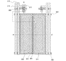
モニター素子部に設ける遮光膜の構成例について図1、図2、及び図13を用いながら説明する。図1は、モニター素子部のレイアウトであり、図2は、図1の鎖線A−A’で切断したときの断面構造図である。また、図13は図1と同じモニター素子部を示すが、モニター素子を駆動するTFTの位置などを分かりやすく説明するために、参照番号212で示される領域では第1の電極207の記載を省略し、参照番号213で示される領域ではさらに電流供給線202、遮光膜214、ドレイン電極215の記載を省略して図示したものである。
A configuration example of the light shielding film provided in the monitor element portion will be described with reference to FIGS. 1, 2, and 13. FIG. 1 is a layout of the monitor element portion, and FIG. 2 is a cross-sectional structure diagram taken along the chain line A-A ′ of FIG. 1. 13 shows the same monitor element portion as FIG. 1, but the description of the
図1、図2、及び図13に示すとおり、モニター素子部において、モニター素子を駆動するTFT211のゲート配線に電位を与える制御線201と画素部の発光素子に設けられたTFTのゲート配線206とで囲まれた領域には、それぞれ第1の電極(陽極または陰極)と電界発光層208と第2の電極(陰極または陽極)209とからなるモニター素子と、当該モニター素子を駆動するTFTとが設けられている。図1、図2、及び図13の点線で囲まれた領域204は、陽極と電界発光層と陰極からなるモニター素子が発光する領域を表している。また、モニター素子を駆動するTFTのゲート配線205は、モニター素子部の第1の電極207に重なっている。また、TFT211が制御線201とゲート配線206とで囲まれた領域に形成されており、TFT211のゲート電極205は遮光膜203と同じ層上に形成されているため、遮光膜203はTFT211と重ならないように形成する必要がある。このため、光を遮光するのに十分な大きさや形状を有する遮光膜203を形成することが困難であった。その結果、TFT211と遮光膜203との間の隙間から、モニター素子から発生した光が漏れる。また、モニター素子を駆動するTFTのソース領域と定電流源とを接続する電流供給線202と、モニター素子を駆動するTFTのゲート配線に電位を与える制御線201との隙間に相当する領域からも光が漏れる。なお、図2において、参照番号210は層間絶縁膜、211は絶縁膜(バンク、隔壁、障壁、土手などと呼ばれる)である。
As shown in FIGS. 1, 2, and 13, in the monitor element portion, a
この光漏れは、モニター素子部の開口率を下げることにより防止することが可能であるが、発光素子の劣化特性を考慮するとモニター素子部の開口率と画素部の開口率は同程度にした方が望ましい。したがって、モニター素子部の開口率を下げることは、画素部の発光素子の温度、劣化補償を行うという本来の目的を達成する上で望ましいものではない。 This light leakage can be prevented by lowering the aperture ratio of the monitor element section, but considering the deterioration characteristics of the light emitting element, the aperture ratio of the monitor element section and the aperture ratio of the pixel section should be the same. Is desirable. Therefore, lowering the aperture ratio of the monitor element portion is not desirable for achieving the original purpose of compensating for the temperature and deterioration of the light emitting element in the pixel portion.
本発明は、工程数を増やすことなく、且つ、コストが高くならないような遮光膜が形成された表示装置を提供することを課題とする。 An object of the present invention is to provide a display device in which a light-shielding film is formed without increasing the number of steps and without increasing the cost.
本発明の表示装置は、発光素子の温度変化、経時変化による影響を抑制するためのモニター素子と、当該モニター素子を駆動するためのTFTとを有し、前記モニター素子と、当該モニター素子を駆動するためのTFTとは、互いに異なる領域にそれぞれ設けられている。すなわち、モニター素子を駆動するためのTFTはモニター素子と重ならないように設けられている。また、本発明の表示装置は、モニター素子の第1の電極と重なるように設けられた第1の遮光膜と、前記第1の電極の外縁部と重なる第2の遮光膜を有する。なお、本明細書において、「モニター素子部」とは、モニター素子が設けられている領域全体を指すものとする。 The display device of the present invention includes a monitor element for suppressing an influence due to a temperature change and a change with time of the light emitting element, and a TFT for driving the monitor element, and the monitor element and the monitor element are driven. The TFTs for this purpose are provided in different regions. That is, the TFT for driving the monitor element is provided so as not to overlap the monitor element. In addition, the display device of the present invention includes a first light-shielding film provided so as to overlap with the first electrode of the monitor element, and a second light-shielding film overlapping with the outer edge portion of the first electrode. In the present specification, the “monitor element portion” refers to the entire region where the monitor element is provided.
また、本発明を適用することが可能な発光素子を有する表示装置は、アクティブマトリックス型である。また、発光素子から発せられる光の射出方式としては、下面射出型または両面射出型が適用できる。 A display device including a light-emitting element to which the present invention can be applied is an active matrix type. As a method for emitting light emitted from the light emitting element, a bottom emission type or a double emission type can be applied.
また、前記第1の遮光膜は、前記モニター素子のゲート信号線や画素部に設けられた発光素子のゲート信号線と同一の作製条件で同時に形成され、前記第2の遮光膜は、前記モニター素子のソース信号線や画素部に設けられた発光素子のソース信号線と同一の作製条件で同時に形成されることを特徴とする。 The first light shielding film is simultaneously formed under the same manufacturing conditions as the gate signal line of the monitor element and the gate signal line of the light emitting element provided in the pixel portion, and the second light shielding film is formed of the monitor element. They are formed simultaneously under the same manufacturing conditions as the source signal line of the element and the source signal line of the light emitting element provided in the pixel portion.
また、本発明の表示装置は、複数の画素と、ソース信号線駆動回路(ソースドライバー)と、ゲート信号線駆動回路(ゲートドライバー)とを有する。そして、複数の画素の各々は、発光素子と、画素へのビデオ信号の入力を制御する第1のトランジスタと、発光素子の点灯または非点灯を制御する第2のトランジスタと、ビデオ信号を保持する容量素子とを有する。なお、容量素子は必ずしも設ける必要はなく、第2のトランジスタのゲート容量で代用することが可能である。 The display device of the present invention includes a plurality of pixels, a source signal line driver circuit (source driver), and a gate signal line driver circuit (gate driver). Each of the plurality of pixels holds a light-emitting element, a first transistor that controls input of a video signal to the pixel, a second transistor that controls lighting or non-lighting of the light-emitting element, and a video signal. And a capacitor. Note that the capacitor is not necessarily provided, and the gate capacitor of the second transistor can be used instead.
また、モニター素子部(モニター素子が設けられている領域)は、画素部内に設けても良いし、それ以外の領域に設けても良い。但し、画像の表示に影響を及ぼさないようにし、且つ、モニター素子部と画素部の発光素子とをなるべく同じ環境下に置くために、モニター素子部は画素部以外の領域に近接して設けることが望ましい。 Further, the monitor element portion (region where the monitor element is provided) may be provided in the pixel portion, or may be provided in other regions. However, in order not to affect the display of the image and to place the monitor element portion and the light emitting element of the pixel portion in the same environment as much as possible, the monitor element portion should be provided close to a region other than the pixel portion. Is desirable.
また、モニター素子の数は適宜選択することができる。すなわち、モニター素子は、1個のみ設ける構成でもよいが、複数設ける構成でもよい。モニター素子を1個のみ用いる場合、定電流源に流す電流値は各画素の発光素子に流したい電流値を設定すればよいため消費電力を削減することができる。また、複数のモニター素子を複数設ける場合、モニター素子毎の特性のばらつきを平均化することができる。 The number of monitor elements can be selected as appropriate. That is, only one monitor element may be provided, or a plurality of monitor elements may be provided. When only one monitor element is used, the current value to be supplied to the constant current source may be set to a current value to be supplied to the light emitting element of each pixel, so that power consumption can be reduced. In addition, when a plurality of monitor elements are provided, it is possible to average variations in characteristics for each monitor element.
また、発光素子を含むパネルを用いてカラー表示を行う場合、発光波長帯の異なる電界発光層を画素毎に設けるとよく、典型的には、赤(R)、緑(G)、青(B)の各色に対応した電界発光層を設けると良い。この場合、赤、緑、青の各色に対応したモニター素子をそれぞれ設けて、各色毎に電源電圧を補正できるようにすると良い。この場合も、各色毎にモニター素子を1個ずつ設ける構成としても良いが、好ましくは各色毎にそれぞれ複数設ける構成が好ましい。 When color display is performed using a panel including a light-emitting element, an electroluminescent layer having a different emission wavelength band is preferably provided for each pixel. Typically, red (R), green (G), and blue (B It is preferable to provide an electroluminescent layer corresponding to each color. In this case, it is preferable to provide monitor elements corresponding to the respective colors of red, green, and blue so that the power supply voltage can be corrected for each color. In this case as well, a configuration may be adopted in which one monitor element is provided for each color, but a configuration in which a plurality of monitor elements are provided for each color is preferable.
本明細書で開示するアクティブマトリクス型の表示装置に関する発明の構成は、
発光素子及び当該発光素子を駆動する第1の薄膜トランジスタを有する画素がマトリクス状に複数設けられた画素部と、
第1の電極、前記第1の電極上に形成された電界発光層、及び前記電界発光層上に形成された第2の電極を有するモニター素子と、
前記モニター素子を駆動する第2の薄膜トランジスタと、
前記モニター素子に一定電流を流す定電流源と、
アンプと、を有し、
前記定電流源は、前記第2の薄膜トランジスタのソース及びドレインの一方、並びに前記アンプの入力に電気的に接続され、
前記第2の薄膜トランジスタのソース及びドレインの他方は、前記モニター素子の一方の電極に電気的に接続され、
前記アンプの出力に、前記第1の薄膜トランジスタを介して前記発光素子の一方の電極が電気的に接続され、
前記モニター素子と、前記第2の薄膜トランジスタとは互いに重ならないように設けられ、
前記モニター素子の第1の電極と重なるように第1の遮光膜が設けられ、
前記モニター素子の第1の電極の端部に重なるように第2の遮光膜が設けられていることを特徴とする。
The structure of the invention related to the active matrix display device disclosed in this specification is
A pixel portion in which a plurality of pixels each having a light emitting element and a first thin film transistor for driving the light emitting element are provided in a matrix;
A monitor element having a first electrode, an electroluminescent layer formed on the first electrode, and a second electrode formed on the electroluminescent layer;
A second thin film transistor for driving the monitor element;
A constant current source for supplying a constant current to the monitor element;
An amplifier, and
The constant current source is electrically connected to one of a source and a drain of the second thin film transistor and an input of the amplifier,
The other of the source and the drain of the second thin film transistor is electrically connected to one electrode of the monitor element,
One electrode of the light emitting element is electrically connected to the output of the amplifier via the first thin film transistor,
The monitor element and the second thin film transistor are provided so as not to overlap each other.
A first light-shielding film is provided so as to overlap the first electrode of the monitor element;
A second light-shielding film is provided so as to overlap with an end portion of the first electrode of the monitor element.
また、本明細書で開示するアクティブマトリクス型の表示装置に関する別の発明の構成は、
発光素子及び当該発光素子を駆動する第1の薄膜トランジスタを有する画素がマトリクス状に複数設けられた画素部と、
第1の電極、前記第1の電極上に形成された電界発光層、及び前記電界発光層上に形成された第2の電極を有するモニター素子と、前記モニター素子を駆動する第2の薄膜トランジスタとを含むモニター素子部と、
前記モニター素子に一定電流を流す定電流源と、
アンプと、を有し、
前記定電流源は、前記第2の薄膜トランジスタのソース及びドレインの一方、並びに前記アンプの入力に電気的に接続され、
前記第2の薄膜トランジスタのソース及びドレインの他方は、前記モニター素子の一方の電極に電気的に接続され、
前記アンプの出力に、前記第1の薄膜トランジスタを介して前記発光素子の一方の電極が電気的に接続され、
前記モニター素子部には、
ゲート信号線と同じ材料で形成された第1の遮光膜と、
前記第1の遮光膜上に形成された層間絶縁膜と、
ソース信号線と同じ材料で形成され、前記層間絶縁膜上に形成された第2の遮光膜と、
前記層間絶縁膜及び前記第2の遮光膜上に形成された前記モニター素子とが設けられ、
前記モニター素子と、前記第2の薄膜トランジスタとは前記ゲート信号線を介して互いに異なる領域に設けられ、
前記層間絶縁膜を介して前記モニター素子の第1の電極と重なるように第1の遮光膜が設けられ、
前記モニター素子の第1の電極の端部に重なるように第2の遮光膜が設けられていることを特徴とする。
Further, another invention relating to an active matrix display device disclosed in this specification includes:
A pixel portion in which a plurality of pixels each having a light emitting element and a first thin film transistor for driving the light emitting element are provided in a matrix;
A monitor element having a first electrode, an electroluminescent layer formed on the first electrode, and a second electrode formed on the electroluminescent layer; a second thin film transistor for driving the monitor element; Including a monitor element unit,
A constant current source for supplying a constant current to the monitor element;
An amplifier, and
The constant current source is electrically connected to one of a source and a drain of the second thin film transistor and an input of the amplifier,
The other of the source and the drain of the second thin film transistor is electrically connected to one electrode of the monitor element,
One electrode of the light emitting element is electrically connected to the output of the amplifier via the first thin film transistor,
In the monitor element section,
A first light-shielding film formed of the same material as the gate signal line;
An interlayer insulating film formed on the first light shielding film;
A second light-shielding film formed of the same material as the source signal line and formed on the interlayer insulating film;
And the monitor element formed on the interlayer insulating film and the second light shielding film,
The monitor element and the second thin film transistor are provided in different regions through the gate signal line,
A first light-shielding film is provided so as to overlap the first electrode of the monitor element via the interlayer insulating film;
A second light-shielding film is provided so as to overlap with an end portion of the first electrode of the monitor element.
また、上記発明の構成において、前記第2の遮光膜は環状であることを特徴とする。 In the configuration of the invention described above, the second light-shielding film is annular.
また、上記発明の構成において、前記表示装置は、下面射出型または両面射出型であることを特徴とする。 In the configuration of the invention described above, the display device is a bottom emission type or a double emission type.
また、上記発明の構成において、前記アンプはボルテージフォロワであることを特徴とする。 In the configuration of the invention described above, the amplifier is a voltage follower.
また、上記発明の構成において、前記モニター素子及び前記モニター素子を駆動するTFTは、前記画素部に近接して設けられていることを特徴とする。 In the above structure of the invention, the monitor element and the TFT for driving the monitor element are provided in the vicinity of the pixel portion.
また、上記発明の構成において、前記画素部は赤を発光する複数の画素、緑を発光する複数の画素、及び青を発光する複数の画素を有し、前記モニター素子及び前記モニター素子を駆動する薄膜トランジスタは、各発光色毎にそれぞれ設けられていることを特徴とする。 In the structure of the invention described above, the pixel portion includes a plurality of pixels that emit red, a plurality of pixels that emit green, and a plurality of pixels that emit blue, and drives the monitor element and the monitor element. The thin film transistor is provided for each emission color.
また、上記発明の構成において、前記モニター素子及び前記発光素子はEL素子であることを特徴とする。 In the above-described structure, the monitor element and the light-emitting element are EL elements.
また、上記発明の構成において、前記モニター素子と前記発光素子は同じ材料を用いて同じ工程で形成されていることを特徴とする。 In the above-described structure, the monitor element and the light-emitting element are formed using the same material and in the same process.
また、本明細書で開示する表示装置に関する別の発明の構成は、上記表示装置を有するELテレビジョンである。 Another structure of the invention related to the display device disclosed in this specification is an EL television including the display device.
また、本明細書で開示するアクティブマトリクス型の表示装置の作製方法に関する発明の構成は、
基板上に下地膜を形成し、
前記下地膜上に半導体層を形成し、
前記半導体層上にゲート絶縁膜を形成し、
前記ゲート絶縁膜上にゲート電極を形成すると同時に第1の遮光膜を形成し、
前記ゲート電極をマスクとして前記半導体層に不純物を添加することによりソース領域及びドレイン領域を形成して、モニター素子を駆動する薄膜トランジスタを形成し、
前記ゲート絶縁膜、前記ゲート電極、及び前記第1の遮光膜上に層間絶縁膜を形成し、
前記ソース領域及び前記ドレイン領域にそれぞれ接続するソース電極及びドレイン電極を形成すると同時に第2の遮光膜を形成し、
前記層間絶縁膜を介して前記第1の遮光膜に重なるように第1の電極を形成し、前記第1の電極上に電界発光層を形成し、前記電界発光層上に第2の電極を形成することにより、前記層間絶縁膜上にモニター素子を形成し、
前記第1の電極の端部は、前期第2の遮光膜と重なっており、
前記モニター素子は、当該モニター素子を駆動する薄膜トランジスタに重ならないように形成されていることを特徴とする。
In addition, the structure of the invention related to a method for manufacturing an active matrix display device disclosed in this specification is as follows.
Form a base film on the substrate,
Forming a semiconductor layer on the base film;
Forming a gate insulating film on the semiconductor layer;
Forming a gate electrode on the gate insulating film and simultaneously forming a first light-shielding film;
A source region and a drain region are formed by adding impurities to the semiconductor layer using the gate electrode as a mask, and a thin film transistor for driving a monitor element is formed,
Forming an interlayer insulating film on the gate insulating film, the gate electrode, and the first light shielding film;
Forming a source electrode and a drain electrode connected to the source region and the drain region, respectively, and simultaneously forming a second light-shielding film;
A first electrode is formed so as to overlap the first light-shielding film through the interlayer insulating film, an electroluminescent layer is formed on the first electrode, and a second electrode is formed on the electroluminescent layer. By forming a monitor element on the interlayer insulating film,
The end of the first electrode overlaps the second light-shielding film in the previous period,
The monitor element is formed so as not to overlap a thin film transistor that drives the monitor element.
本発明は、モニター素子が設けられた領域(モニター素子部)において、前記モニター素子が設けられた領域と、当該モニター素子を駆動する薄膜トランジスタが設けられた領域とが、互いに異なることを特徴とする。すなわち、モニター素子を駆動する薄膜トランジスタが、モニター素子に重ならないことを特徴とする。そして、モニター素子を駆動するTFTのゲート電極及びゲート信号線を形成するために用いる導電膜を用いて第1の遮光膜を形成する。さらに、ソース信号線を形成するために用いる導電膜を用いて第2の遮光膜を形成する。このように2つの遮光膜を形成することによって、工程数を増やすことなく信頼性の高い遮光膜を形成することができる。また、歩留まり、信頼性の高い表示装置を安価に提供することができる。 The present invention is characterized in that, in a region where a monitor element is provided (monitor element portion), a region where the monitor element is provided and a region where a thin film transistor for driving the monitor element is provided are different from each other. . That is, the thin film transistor for driving the monitor element does not overlap with the monitor element. Then, a first light-shielding film is formed using a conductive film used for forming a gate electrode and a gate signal line of a TFT for driving the monitor element. Further, a second light-shielding film is formed using a conductive film used for forming the source signal line. By forming two light shielding films in this way, a highly reliable light shielding film can be formed without increasing the number of steps. In addition, a display device with high yield and reliability can be provided at low cost.
本発明を実施するための最良の形態を、図面を用いながら説明する。但し、本発明は以下の説明に限定されず、本発明の趣旨及びその範囲から逸脱することなくその形態及び詳細を様々に変更し得ることは当業者であれば容易に理解される。従って、本発明は以下に示す実施の形態の記載内容に限定して解釈されるものではない。なお、以下に説明する本発明の構成において、同一部分又は同様な機能を有する部分には同一の符号を異なる図面間で共通して用い、その繰り返しの説明は省略する。 The best mode for carrying out the present invention will be described with reference to the drawings. However, the present invention is not limited to the following description, and it is easily understood by those skilled in the art that modes and details can be variously changed without departing from the spirit and scope of the present invention. Therefore, the present invention should not be construed as being limited to the description of the embodiments below. Note that in structures of the present invention described below, the same portions or portions having similar functions are denoted by the same reference numerals in different drawings, and description thereof is not repeated.
(実施の形態1)
本実施の形態では、モニター素子部に設けられた遮光膜の特徴について説明する。
(Embodiment 1)
In this embodiment mode, characteristics of the light shielding film provided in the monitor element portion will be described.
モニター素子が設けられた領域におけるレイアウト図を図3に示す。また、図3の鎖線A−A’で切断したときの断面構造図を図4(A)に示す。 FIG. 3 shows a layout diagram in the region where the monitor element is provided. FIG. 4A shows a cross-sectional structure diagram taken along the chain line A-A ′ in FIG. 3.
第1の遮光膜301は、ゲートドライバーに接続されたゲート信号線302と同一の層で形成された導電膜である。また、第1の遮光膜301、ゲート信号線302は、モニター素子を駆動するためのTFT310のゲート配線303とも同一の層で形成されている。そして、第1の遮光膜301は、モニター素子の第1の電極321と重なるように設けられている。第1の遮光膜301は、2つのゲート信号線302、2つの電流供給線312で囲まれる領域において、少なくともゲート信号線302と重ならないように設けられている。なお、遮光膜301は、電流供給線312と重なるように設けられていてもよい。
The first
第2の遮光膜311は、モニター素子を駆動するTFT310のソース領域と、定電流源とを接続する電流供給線312と同一の層で形成された導電膜である。この第2の遮光膜311は、TFT310のドレイン電極としても機能している。また、第2の遮光膜311、電流供給線312は、TFT310のゲート配線303に電位を与える制御線313とも同一の層で形成されている。そして、第2の遮光膜311は、環状の形状をしており、第1の電極321の外周(外縁)部分を覆うように設けられている。このように第2の遮光膜311を設けることにより、第1の遮光膜301のみでは第1の電極321を覆いきれていなかった領域も覆うことができる。なお、参照番号324は絶縁膜(バンク、隔壁、障壁、土手などと呼ばれる)である。
The second
なお、第1の電極321は、電界発光層320に電位を与えるための一方の電極であり、陽極または陰極として機能する。また、図3及び図4(A)において、点線で示される発光領域322は、第1の電極321と第2の電極323とにそれぞれ電位を与えたときに発光素子が発光する領域である。
Note that the
本実施の形態では、下面照射型の表示装置において、マトリクス状に並んだ複数の画素に対して、モニター素子と駆動TFTが1つおきに複数配列されている。すなわち、モニター素子と、モニター素子を駆動するTFTとは、ゲート信号線を介して互いに異なる領域に設けられている。また、モニター素子の発光する光が漏れないようにするために、第1の遮光膜301と第2の遮光膜311が第1の電極321と重なっている。当該構造により、モニター素子が発光する光を十分に遮光することができる。
In this embodiment mode, in the bottom-illuminated display device, a plurality of monitor elements and drive TFTs are arranged alternately for a plurality of pixels arranged in a matrix. In other words, the monitor element and the TFT for driving the monitor element are provided in different regions through the gate signal line. In addition, the first
また、第1の遮光膜301と第2の遮光膜311は、それぞれモニター素子を駆動するためのTFT310を形成する際の配線と同一の工程で形成されている。このため、余計なコストや工程数を増やすことなく遮光膜を形成することができる。
In addition, the first
ここで、モニター素子部と同一基板上に形成されている、画素部に設けられた下面射出構造(ボトムエミッション方式)の発光素子について図7を用いて説明する。 Here, a light-emitting element having a bottom emission structure (bottom emission method) provided in the pixel portion, which is formed over the same substrate as the monitor element portion, will be described with reference to FIG.
陽極として機能する第1の電極1302に用いる材料としては、仕事関数の大きい材料を用いることが望ましい。例えば、ITO(インジウムスズ酸化物)膜、インジウム亜鉛酸化物(IZO)膜などの透明導電膜を用いることができる。透明性を有する導電膜を用いることで光を透過させることが可能な陽極を形成することができる。なお、第1の電極1302はTFT1301と接続されている。
As a material used for the
また、陰極として機能する第2の電極1304に用いる材料としては、仕事関数の小さい材料(Al、Ag、Li、Ca、またはこれらの合金であるMgAg、MgIn、AlLi、CaF2、または窒化カルシウム)からなる金属膜を用いることができる。こうして、光を反射する金属膜を用いることで光が透過しない陰極を形成することができる。なお、1303は電界発光層を示している。
In addition, as a material used for the
こうして、図7において矢印で示すように画素部に設けられた発光素子からの光を下面に取り出すことが可能になる。また、画素部に設けられた下面射出構造の発光素子を表示装置に用いる場合には基板1300は光透過性を有する基板を用いる。また、光学フィルムを設ける場合には、基板1300に光学フィルムを設ければよい。
(本実施の形態2)
In this manner, light from the light emitting element provided in the pixel portion can be extracted to the lower surface as indicated by an arrow in FIG. In the case where a light-emitting element having a bottom emission structure provided in the pixel portion is used for a display device, the
(Embodiment 2)
本実施の形態では、モニター素子部において層間絶縁膜を2層形成する場合の遮光膜を有する表示装置の構成について、図4(B)を用いながら説明する。なお、本実施の形態では、実施の形態1と相違する点のみについて説明する。 In this embodiment mode, a structure of a display device including a light-blocking film in the case where two interlayer insulating films are formed in a monitor element portion will be described with reference to FIG. In the present embodiment, only differences from the first embodiment will be described.
実施の形態1では、図4(A)に示すように層間絶縁膜が1層のみ形成されているため、層間絶縁膜331上において第1の電極321が第2の遮光膜311に接して形成されているのに対し、本実施の形態では、層間絶縁膜が2層形成されている。そして、第1の電極321の外縁部(端部)が、2層目の層間絶縁膜332を挟んで第2の遮光膜311と重なっている。なお図4(B)では、第2の遮光膜311が環状の形状を有する例を示しているが、本発明はこれに限定されない。すなわち、2層目の層間絶縁膜332を挟んで第1の電極321と第2の遮光膜311と重なる場合は、第2の遮光膜311は、第1の遮光膜301とゲート配線302との間の隙間を少なくとも遮光するような形状を有していればよい。また、本実施の形態においても、モニター素子が設けられた領域と、当該モニター素子を駆動するTFTが設けられた領域とが、互いに重ならないように配置されているため、第1の遮光膜301及び第2の遮光膜311によって、表示装置から光が外部に漏れないような構造とすることができる。
In
(実施の形態3)
本実施の形態では、表示装置のモニター素子部の作製工程について説明する。なお、表示装置の画素部に設けられる薄膜トランジスタや発光素子は、モニター素子部に設けられる薄膜トランジスタやモニター素子と同一の作製条件、作製工程を用いて形成すればよいため、画素部の作製工程についての説明をここでは省略する。
(Embodiment 3)
In this embodiment mode, a manufacturing process of a monitor element portion of a display device will be described. Note that a thin film transistor or a light-emitting element provided in the pixel portion of the display device may be formed using the same manufacturing conditions and manufacturing steps as those of the thin film transistor and the monitor element provided in the monitor element portion. The description is omitted here.
図5、図6は、上面図である図8の鎖線B−B´における断面を示す図である。まず、図5(A)に示すように、絶縁基板101の上に下地膜102を形成する。絶縁基板101は、例えばバリウムホウケイ酸ガラスや、アルミノホウケイ酸ガラスなどのガラス基板、石英基板、セラミック基板等を用いることができる。また、プラスチック等の可撓性を有する合成樹脂からなる基板は、一般的に上記基板と比較して耐熱温度が低い傾向にあるが、作製工程における処理温度に耐え得るのであれば用いることが可能である。また、絶縁基板101の表面をCMP法などによって研磨し、平坦化しておいてもよい。
5 and 6 are cross-sectional views taken along the chain line BB ′ of FIG. 8 which is a top view. First, as illustrated in FIG. 5A, the
また、下地膜102の成膜方法は、プラズマCVD法や低圧CVD法に代表されるCVD法、スパッタ法などの公知の方法を用いればよい。また、下地膜としては、酸化珪素膜、窒化珪素膜、酸化窒化珪素膜、窒化酸化珪素膜のいずれか一を用いる単層構造としてもよいし、これらを適宜積層する構造としてもよい。なお、本明細書中において、酸化窒化珪素とは酸素の組成比が窒素の組成比より大きい物質のことを指し、窒素を含む酸化珪素ということもできる。また、本明細書中において、窒化酸化珪素とは窒素の組成比が酸素の組成比より大きい物質のことを指し、酸素を含む窒化珪素ということもできる。本実施の形態では、下地膜として、窒化酸化珪素膜、酸化窒化珪素膜を順に積層する構成とする。
As a method for forming the
次に、下地膜102の上に半導体膜103を形成する。半導体膜103としては、非晶質半導体膜を形成すればよいが、微結晶半導体膜や結晶性半導体膜を形成してもよい。また、半導体膜の材料に限定はないが、好ましくはシリコンまたはシリコンゲルマニウムを用いるとよい。本実施の形態では、非晶質珪素膜を形成する。なお、半導体膜を形成した後に、半導体膜に含まれる水素を除去する工程を行ってもよい。
Next, the
また、下地膜102と半導体膜103を形成する際に、下地膜102と半導体膜103との界面が大気に曝されないようにすると、界面の汚染を防ぐことが可能となり、作製されるTFTの特性のバラツキを低減させることができる。本実施の形態では、下地膜102と半導体膜103を、プラズマCVD法を用いて大気に曝さずに連続して形成する。
In addition, when the
次に、半導体膜103を公知の方法(レーザー結晶化法、熱結晶化法、またはニッケルなどの結晶化を促進する元素を用いた熱結晶化方法など)により結晶性半導体膜を形成する。ここで、結晶化の後に、ボロン(B)などのp型の導電型を付与する不純物を結晶性半導体膜の全面にドーピングして、TFTのチャネル形成領域となる領域にチャネルドープし、TFTのしきい値電圧を制御するようにしてもよい。なお、本実施の形態では半導体膜103を結晶化した結晶性半導体膜を用いているが、結晶性半導体膜の代わりに非晶質の半導体膜を用いることも可能である。
Next, a crystalline semiconductor film is formed from the
次に、図5(B)に示すように、結晶性半導体膜をパターニングして結晶性半導体層104(島状半導体層)を形成する。なお、図8(A)は、結晶性半導体層104の上面図を示している。本明細書において、「パターニング」とは、所望の形状にエッチングすることを指す。
Next, as shown in FIG. 5B, the crystalline semiconductor film is patterned to form a crystalline semiconductor layer 104 (island semiconductor layer). Note that FIG. 8A illustrates a top view of the
次に、パターニングされた結晶性半導体層104上にゲート絶縁膜105を形成する。ゲート絶縁膜105は、酸化珪素膜、窒化珪素膜、酸化窒化珪素膜、窒化酸化珪素膜のいずれか一を用いる単層構造としてもよいし、これらを適宜積層する構造としてもよい。
Next, a
次に、図5(C)、図8(B)に示すように、ゲート絶縁膜105の上にゲート配線106(ゲート電極)を形成すると同時に、第1の遮光膜151、ゲートドライバーに接続されるゲート信号線160を形成する。なお、第1の遮光膜151は、後の工程で作製する第1の電極110と重なるように形成しておく。また、第1の遮光膜151はモニター素子部に設けるものであり、画素部の発光素子に設けるものではない。ゲート配線106及び第1の遮光膜151の材料としては、アルミニウム、モリブデン、チタン、及び炭素のうち少なくとも一種、又は複数種を含むものを用いればよい。このとき、モリブデン、またはチタンの組成比は7.0〜20atoms%であることが好ましい。
Next, as shown in FIGS. 5C and 8B, a gate wiring 106 (gate electrode) is formed on the
次に、ゲート配線106をマスクとして、ボロン(B)などのp型の導電型を付与する不純物を結晶性半導体層104にドーピングする。本工程により、TFTのソース領域及びドレイン領域を自己整合的に形成することができる。なお、本実施の形態では、公知のドーピング方法により、TFTのチャネル形成領域とソース領域及びドレイン領域との間に低濃度不純物領域(LDD領域)を形成しているが、低濃度不純物領域を設けない構成としてもよい。
Next, using the
また、ドーピングを行った後、不純物領域にドーピングされた不純物元素を活性化するために、加熱処理、強光の照射、又はレーザー光の照射を行ってもよい。これにより、不純物元素の活性化だけでなく、ゲート絶縁膜105へのプラズマダメージやゲート絶縁膜105と結晶性半導体層104との界面へのプラズマダメージを回復することができる。
In addition, after the doping, heat treatment, intense light irradiation, or laser light irradiation may be performed in order to activate the impurity element doped in the impurity region. Accordingly, not only activation of the impurity element but also plasma damage to the
次に、図5(D)に示すように、ゲート絶縁膜105及びゲート配線106上に第1の層間絶縁膜107を形成する。本実施の形態では、窒化酸化珪素膜、酸化窒化珪素膜を順に積層する構成とする。
Next, as illustrated in FIG. 5D, a first
第1の層間絶縁膜107を形成した後、窒素雰囲気中で、300〜550℃(より好ましくは400〜500℃)で1〜12時間の熱処理を行い、パターニングされた結晶性半導体層104(半導体層)を水素化する工程を行うことが好ましい。本工程により、第1の層間絶縁膜107に含まれている水素により半導体層のダングリングボンドを終端することができる。本実施の形態では、410℃で1時間加熱処理を行う。
After the formation of the first
次に、TFTのソース領域及びドレイン領域に達するように、第1の層間絶縁膜107にコンタクトホールを形成する。コンタクトホールの形状は、テーパー状にするとよい。
Next, contact holes are formed in the first
次に、図6(A)、図8(C)に示すように、コンタクトホールを覆うように配線108(電流供給線)を形成すると同時に第2の遮光膜152、制御線154を形成する。配線108はソース電極(または電流供給線)として機能し、第2の遮光膜152は、遮光だけではなくドレイン電極としても機能している。また、図8(C)に示す上面図のように、第2の遮光膜152は、上面から見て第1の遮光膜151上に、少なくとも第1の遮光膜151とゲート信号線160との間の領域と重なるように設けられており、環状の形状を有している。また、第2の遮光膜152はモニター素子に設けるものであり、画素部の発光素子に設けるものではない。
Next, as shown in FIGS. 6A and 8C, the wiring 108 (current supply line) is formed so as to cover the contact hole, and at the same time, the second
配線108及び第2の遮光膜152の材料としては、Ag、Au、Cu、Ni、Pt、Pd、Ir、Rh、W、Al、Ta、Mo、Cd、Zn、Fe、Ti、Zr、Ba等の金属若しくはその合金、またはその金属窒化物を用いるか、SiやGeの如き半導体材料を用いて形成する。また、これらの積層構造としてもよい。本実施の形態では、チタン(Ti)を100nm形成し、アルミニウムとシリコンの合金(Al−Si)を700nm形成し、チタン(Ti)を200nm形成し、所望な形状にパターニングする。
Examples of materials for the
次に、図6(B)、図8(D)に示すように、第1の層間絶縁膜107及び第2の遮光膜152に接して第1の電極110を形成する。図8(D)に示す上面図のように、第1の電極110は、上面から見て第1の遮光膜151上に全て配置されるように設けられている。また、第1の電極110の外縁部は、第2の遮光膜152の上面及び側面に接する構造となっている。
Next, as shown in FIGS. 6B and 8D, the
また、本実施の形態では、画素部の発光素子からの光を第1の電極110側から取り出す構造にするため、透光性を有する膜を用いて第1の電極110を形成する。第1の電極110としては、酸化珪素を含む酸化インジウムスズ(酸化珪素を含むインジウム錫酸化物ともいう。以下、「ITSO」という。)、酸化亜鉛、酸化スズ、酸化インジウムなどを用いることができる。また、酸化インジウムに2〜20atomic%の酸化亜鉛(ZnO)を混合した酸化インジウム酸化亜鉛合金などの透明導電膜を用いることもできる。また、上記透明導電膜の他に、窒化チタン膜またはチタン膜を用いてもよい。この場合、透明導電膜を成膜した後に、窒化チタン膜またはチタン膜を、光が透過する程度の膜厚(好ましくは5〜30nm程度)で成膜する。本実施の形態では、第1の電極110としてITSO膜を110nm形成する。
In this embodiment mode, the
また、第1の電極110は、その表面が平坦化されるように、CMP法、ポリビニルアルコール系の多孔質体で拭浄し、研磨してもよい。またCMP法を用いた研磨後に、第1の電極110の表面に紫外線照射、酸素プラズマ処理などを行ってもよい。
Further, the
なお、本実施の形態では、pチャネル型のTFTを作製する工程について説明した。しかし、ゲート電極をマスクとして結晶性半導体層104にn型の導電型を付与する不純物をドーピングすることによりnチャネル型のTFTを作製する際にも本発明は適用することができる。また、同一基板上にpチャネル型のTFTとnチャネル型のTFTを作製する場合についても、本発明を適用することができる。
Note that in this embodiment, the process for manufacturing a p-channel TFT has been described. However, the present invention can also be applied to manufacturing an n-channel TFT by doping an impurity imparting n-type conductivity into the
また、TFTは結晶性半導体層104にチャネル形成領域が一つ形成されるシングルゲート構造でもよいし、二つ形成されるダブルゲート構造または三つ形成されるトリプルゲート構造であってもよい。また、周辺駆動回路領域の薄膜トランジスタも、シングルゲート構造、ダブルゲート構造またはトリプルゲート構造であってもよい。
The TFT may have a single gate structure in which one channel formation region is formed in the
また、本実施の形態で示したTFTの作製方法に限らず、トップゲート型(プレーナー型)、ボトムゲート型(逆スタガ型)、あるいはチャネル形成領域の上下にゲート絶縁膜を介して配置された2つのゲート電極を有する、デュアルゲート型やその他の構造においても本発明を適用することができる。 In addition to the TFT manufacturing method described in this embodiment mode, a top gate type (planar type), a bottom gate type (reverse stagger type), or a channel formation region is disposed above and below a gate insulating film. The present invention can also be applied to a dual gate type or other structure having two gate electrodes.
次に、図6(C)に示すように、第1の電極110の端部及びTFTを覆うように絶縁膜111(バンク、隔壁、障壁、土手などと呼ばれる。)を形成する。
Next, as illustrated in FIG. 6C, an insulating film 111 (referred to as a bank, a partition, a barrier, a bank, or the like) is formed so as to cover the end portion of the
絶縁膜111としては、酸化珪素、窒化珪素、酸化窒化珪素、酸化アルミニウム、窒化アルミニウム、酸窒化アルミニウムその他の無機絶縁性材料、又はアクリル酸、メタクリル酸及びこれらの誘導体、又はポリイミド(polyimide)、芳香族ポリアミド、ポリベンゾイミダゾール(polybenzimidazole)などの耐熱性高分子、又はシロキサン系材料を出発材料として形成された珪素、酸素、水素からなる化合物のうちSi−O−Si結合を含む無機シロキサン、珪素上の水素がメチル基やフェニル基のような有機基によって置換された有機シロキサン系の絶縁性材料を用いることができる。アクリル、ポリイミド等の感光性、非感光性の材料を用いて形成してもよい。本実施の形態では、感光性ポリイミドを用いて、平坦な領域で膜厚が1.5μmとなるように絶縁膜111を形成する。
As the insulating
また、絶縁膜111は曲率半径が連続的に変化する形状が好ましく、絶縁膜111上に形成される電界発光層(有機化合物を含む層)、第2の電極の被覆性を向上させることができる。
In addition, the insulating
また、信頼性をさらに向上させるため、電界発光層を形成する前に加熱処理を行うとよい。当該加熱処理により、第1の電極110や絶縁膜111に含有、付着している水分を放出させることが好ましい。
In order to further improve the reliability, heat treatment may be performed before forming the electroluminescent layer. By the heat treatment, moisture contained in and attached to the
次に、図10に示すように、第1の電極110上に電界発光層112を形成する。なお、図10は、図3及び図8(D)の鎖線B−B’における断面図に相当する。また、図10では1つのモニター素子しか図示していないが、本実施の形態では赤(R)、緑(G)、青(B)の各色に対応した電界電極を作り分けている。本実施の形態では電界発光層112として、赤(R)、緑(G)、青(B)の発光を示す材料を、蒸着マスクを用いた蒸着法によって、それぞれ選択的に形成する。赤色(R)、緑色(G)、青色(B)の発光を示す材料は、蒸着マスクを用いた蒸着法によってそれぞれ選択的に形成する方法や、液滴吐出法により形成することができる。液滴吐出法の場合、マスクを用いずにRGBの塗り分けを行うことができるという利点がある。本実施の形態では、赤(R)、緑(G)、青(B)の発光を示す材料を蒸着法によってそれぞれ形成する。
Next, as illustrated in FIG. 10, the
電界発光層は、公知の有機発光材料または無機発光材料を用いることができる。また、有機発光材料には低分子系(モノマー系)材料と高分子系(ポリマー系)材料があるがどちらを用いても良い。また、電界発光層の構造は正孔注入層、正孔輸送層、発光層、電子輸送層または電子注入層などを自由に組み合わせて積層構造または単層構造とすればよい。 A known organic light emitting material or inorganic light emitting material can be used for the electroluminescent layer. The organic light emitting material includes a low molecular (monomer) material and a high molecular (polymer) material, either of which may be used. The structure of the electroluminescent layer may be a stacked structure or a single layer structure by freely combining a hole injection layer, a hole transport layer, a light emitting layer, an electron transport layer, an electron injection layer, or the like.
なお、電界発光層の蒸着前に、不活性ガスを主成分とし、酸素の濃度が5%以下且つ水の濃度が1%以下とする雰囲気で加熱処理を行い、水分などを除去することが好ましい。本実施の形態では、300℃で1時間加熱処理を行う。 Note that before the electroluminescent layer is deposited, it is preferable to perform heat treatment in an atmosphere containing an inert gas as a main component, an oxygen concentration of 5% or less, and a water concentration of 1% or less to remove moisture and the like. . In this embodiment, heat treatment is performed at 300 ° C. for 1 hour.
次に、電界発光層112の上に導電膜からなる第2の電極113を形成する。なお、第1の電極110が陽極として機能するときは第2の電極113は陰極として機能し、第1の電極110が陰極として機能するときは第2の電極113は陽極として機能する。また、
第2の電極113の材料としては、仕事関数の小さい材料(Al、Ag、Li、Ca、またはこれらの合金MgAg、MgIn、AlLi、CaF2、または窒化カルシウム)を用いればよい。
Next, a
As a material for the
以上の工程により、第1の電極110、電界発光層112、及び第2の電極113からなるモニター素子が形成される。このモニター素子が発光する領域は、図8(D)における発光領域153で表わされる。発光領域153は、第1の遮光膜151及び第2の遮光膜152により、基板側から光が漏れないように遮蔽されている。
Through the above steps, a monitor element including the
図10に示す表示装置において、モニター素子から発した光は、基板101と第1の電極110の間に形成された膜を透過して第1の電極110側から矢印の方向に射出されるが、第1の遮光膜151及び第2の遮光膜152により遮光される。
In the display device illustrated in FIG. 10, light emitted from the monitor element passes through a film formed between the
また、第2の電極113を覆うようにしてパッシベーション膜を設けることは有効である。パッシベーション膜としては、窒化珪素、酸化珪素、酸化窒化珪素、窒化酸化珪素、窒化アルミニウム、酸素含有量が窒素含有量よりも多い酸化窒化アルミニウム(AlON)、窒素含有量が酸素含有量よりも多い窒化酸化アルミニウム(AlNO)、酸化アルミニウム、ダイヤモンドライクカーボン(DLC)、または窒素含有炭素膜(CN)を含む絶縁膜からなり、該絶縁膜を単層もしくは組み合わせた積層を用いることができる。また、シリコン(Si)と酸素(O)との結合で骨格構造が構成され、置換基に少なくとも水素を含む材料、もしくは置換基にフッ素、アルキル基、または芳香族炭化水素のうち少なくとも1種を有する材料を用いてもよい。
In addition, it is effective to provide a passivation film so as to cover the
この際、カバレッジの良い膜をパッシベーション膜として用いることが好ましく、炭素膜、特にDLC膜を用いることは有効である。DLC膜は室温から100℃以下の温度範囲で成膜可能であるため、耐熱性の低い電界発光層112の上方にも容易に成膜することができる。また、DLC膜は酸素に対するブロッキング効果が高く、電界発光層112の酸化を抑制することが可能である。そのため、この後に続く封止工程を行う間に電界発光層112が酸化するといった問題を防止することができる。
At this time, it is preferable to use a film with good coverage as the passivation film, and it is effective to use a carbon film, particularly a DLC film. Since the DLC film can be formed in a temperature range from room temperature to 100 ° C., it can be easily formed over the
次に、発光素子及びモニター素子が形成された基板101と、封止基板とをシール材によって固着し、発光素子及びモニター素子を封止する。断面からの水分の侵入がシール材によって遮断されるので、発光素子の劣化が防止でき、表示装置の信頼性が向上する。なお、シール材で囲まれた領域には充填材を充填してもよく、窒素雰囲気下で封止することによって、窒素等を封入してもよい。また充填材は、液状の状態で滴下し、表示装置内に充填することもできる。本実施の形態は、下面射出型のため、透光性を有する充填材を使用する必要はないが、充填材を透過して光を取り出す構造の場合は、透光性を有す材料を用いて充填材を形成する必要がある。充填材の一例としては、可視光硬化、紫外線硬化または熱硬化のエポキシ樹脂が挙げられる。以上の工程において、発光素子を有する表示装置が完成する。
Next, the
なお、シール材としては、紫外線硬化樹脂、熱硬化樹脂、シリコーン樹脂、エポキシ樹脂、アクリル樹脂、ポリイミド樹脂、フェノール樹脂、PVC(ポリビニルクロライド)、PVB(ポリビニルブチラル)またはEVA(エチレンビニルアセテート)を用いることが可能である。また、シール材はフィラ−(棒状またはファイバー状のスペーサ)や球状のスペーサを添加したものであっても良い。 In addition, as a sealing material, ultraviolet curable resin, thermosetting resin, silicone resin, epoxy resin, acrylic resin, polyimide resin, phenol resin, PVC (polyvinyl chloride), PVB (polyvinyl butyral), or EVA (ethylene vinyl acetate). It is possible to use. Further, the sealing material may be a filler (a rod-like or fiber-like spacer) or a spherical spacer added.
また、素子の水分による劣化を防ぐために表示パネル内に乾燥剤を設置することが好ましい。本実施の形態では、画素部やモニター素子部を取り囲むように封止基板に形成された凹部に乾燥剤を設置し、薄型化を妨げない構成とする。また、ゲート配線層に対応する領域にも乾燥剤を設置することにより吸水面積を広く取ることができ、吸水効果が高い。また、直接発光しないゲート配線層上に乾燥剤を形成しているので、画素部の光取り出し効率を低下させることもない。 Further, it is preferable to install a desiccant in the display panel in order to prevent deterioration of the element due to moisture. In this embodiment mode, a desiccant is provided in a concave portion formed in the sealing substrate so as to surround the pixel portion and the monitor element portion, and the thickness is not hindered. In addition, by installing a desiccant in the region corresponding to the gate wiring layer, the water absorption area can be increased, and the water absorption effect is high. Further, since the desiccant is formed on the gate wiring layer that does not emit light directly, the light extraction efficiency of the pixel portion is not lowered.
なお、本実施の形態では、ガラス基板で発光素子を封止した場合を説明するが、封止の処理とは、発光素子を水分から保護するための処理であり、カバー材で機械的に封入する方法、熱硬化性樹脂又は紫外光硬化性樹脂で封入する方法、金属酸化物や窒化物等のバリア能力が高い薄膜により封止する方法のいずれかを用いる。カバー材としては、ガラス、セラミックス、プラスチックもしくは金属を用いることができるが、カバー材側に光を射出させる場合は透光性でなければならない。また、カバー材と上記発光素子が形成された基板とは熱硬化性樹脂又は紫外光硬化性樹脂等のシール材を用いて貼り合わせられ、熱処理又は紫外光照射処理によって樹脂を硬化させて密閉空間を形成する。この密閉空間の中に酸化バリウムに代表される吸湿材を設けることも有効である。この吸湿材は、シール材の上に接して設けても良いし、発光素子よりの光を妨げないような、隔壁の上や周辺部に設けても良い。さらに、カバー材と発光素子の形成された基板との空間を熱硬化性樹脂若しくは紫外光硬化性樹脂で充填することも可能である。この場合、熱硬化性樹脂若しくは紫外光硬化性樹脂の中に酸化バリウムに代表される吸湿材を添加しておくことは有効である。 Note that in this embodiment, the case where a light-emitting element is sealed with a glass substrate is described; however, the sealing process is a process for protecting the light-emitting element from moisture and is mechanically sealed with a cover material. Or a method of encapsulating with a thermosetting resin or an ultraviolet light curable resin, or a method of encapsulating with a thin film having a high barrier ability such as a metal oxide or nitride. As the cover material, glass, ceramics, plastic, or metal can be used. However, when light is emitted to the cover material side, it must be translucent. In addition, the cover material and the substrate on which the light emitting element is formed are bonded together using a sealing material such as a thermosetting resin or an ultraviolet light curable resin, and the resin is cured by heat treatment or ultraviolet light irradiation treatment to form a sealed space. Form. It is also effective to provide a hygroscopic material typified by barium oxide in this sealed space. This hygroscopic material may be provided in contact with the sealing material, or may be provided on the partition wall or in the peripheral portion so as not to block light from the light emitting element. Further, the space between the cover material and the substrate on which the light emitting element is formed can be filled with a thermosetting resin or an ultraviolet light curable resin. In this case, it is effective to add a moisture absorbing material typified by barium oxide in the thermosetting resin or the ultraviolet light curable resin.
また、カバー材としてガラス基板またはプラスチック基板を用いる。プラスチック基板としては、ポリイミド、ポリアミド、アクリル樹脂、エポキシ樹脂、PES(ポリエチレンサルファイル)、PC(ポリカーボネート)、PET(ポリエチレンテレフタレート)もしくはPEN(ポリエチレンナフタレート)を板状もしくはフィルム状にして用いることができる。 Further, a glass substrate or a plastic substrate is used as the cover material. As the plastic substrate, polyimide, polyamide, acrylic resin, epoxy resin, PES (polyethylene sulfide), PC (polycarbonate), PET (polyethylene terephthalate) or PEN (polyethylene naphthalate) may be used in the form of a plate or film. it can.
なお、密閉空間には乾燥した不活性ガスが充填されている。シール材で囲まれた内側の密閉空間は乾燥剤によって微量な水分が除去され、十分乾燥されている。また、乾燥剤としては、酸化カルシウムや酸化バリウムなどのようなアルカリ土類金属の酸化物のような化学吸着によって水分を吸収する物質を用いることが可能である。なお、他の乾燥剤として、ゼオライトやシリカゲル等の物理吸着によって水分を吸着する物質を用いても良い。 The sealed space is filled with a dry inert gas. A small amount of moisture is removed from the inner sealed space surrounded by the sealing material with a desiccant and is sufficiently dried. As the desiccant, it is possible to use a substance that absorbs moisture by chemical adsorption, such as an oxide of an alkaline earth metal such as calcium oxide or barium oxide. As another desiccant, a substance that adsorbs moisture by physical adsorption, such as zeolite or silica gel, may be used.
また、必要であれば、発光素子からの光の射出面に偏光板または円偏光板(楕円偏光板を含む)、位相差板(λ/4板、λ/2板)、カラーフィルタなどの光学フィルムを適宜設けても良い。また、偏光板または円偏光板に反射防止膜を設けても良い。例えば、表面の凹凸により反射光を拡散し、映り込みを低減できるアンチグレア処理を施すことができる。また、偏光板または円偏光板に加熱処理を施すアンチリフレクション処理を施しても良い。その後さらに、外部衝撃から保護するためハードコート処理を施すと良い。 Further, if necessary, on the light emission surface of the light emitting element, optical films such as a polarizing plate or a circular polarizing plate (including an elliptical polarizing plate), a retardation plate (λ / 4 plate, λ / 2 plate), a color filter, etc. A film may be provided as appropriate. Further, an antireflection film may be provided on the polarizing plate or the circularly polarizing plate. For example, anti-glare treatment can be performed that diffuses reflected light due to surface irregularities and reduces reflection. Moreover, you may perform the anti-reflection process which heat-processes to a polarizing plate or a circularly-polarizing plate. Thereafter, a hard coat treatment may be applied to protect from external impacts.
(実施の形態4)
本実施の形態では、画素部に設けられた発光素子と、モニター素子部に設けられたモニター素子とを有する表示装置の構成について、図11を用いながら説明する。本実施の形態における表示装置は、ゲートドライバー2107、ソースドライバー2108、画素部2109を有する。また、画素部2109の脇に近接して設けられたモニター素子部2110を有する。モニター素子部2110には、RGBの各色毎に対応して、3列分設けられている。また、各列において、モニター素子が設けられた行と、当該モニター素子を駆動するTFTが設けられた行とが、交互に配列されている。すなわち、モニター素子と、モニター素子を駆動するTFTは、マトリクス状に設けられた画素部の発光素子の1列分の半分に相当する個数がそれぞれ設けられている。なお、モニター素子を駆動するTFTは、nチャネル型TFT、pチャネル型TFTのどちらを用いてもよいが、本実施の形態では、pチャネル型TFTを用いる。
(Embodiment 4)
In this embodiment, a structure of a display device including a light-emitting element provided in a pixel portion and a monitor element provided in a monitor element portion will be described with reference to FIGS. The display device in this embodiment includes a
本実施の形態に示す表示装置は、モニター素子部2110に設けられたモニター素子と画素部に設けられた発光素子とが、同一の基板上に設けられている。つまり、発光素子とモニター素子とは、同一の作製条件により、同一の工程で作製されたものであり、環境温度の変化と経時変化に対して概略同じ特性を得ることができる。また、発光素子とモニター素子部の開口率を同程度としているため、同じ劣化特性を有する。
In the display device described in this embodiment, the monitor element provided in the
定電流源2201aは、モニター素子2202aの一方の電極(陽極)と、ボルテージフォロワ回路2203aの非反転入力端子に接続されている。また、モニター素子2202aの他方の電極(陰極)は、接地電位と接続されている。また、ボルテージフォロワ回路2203aの出力端子は、画素部2109に設けられた発光素子を駆動するTFTを介して発光素子の一方の電極と接続されている。
The constant
信号線S1に接続されている画素がRの発光をする画素、信号線S2に接続されている画素がGの発光をする画素、信号線S3に接続されている画素がBの発光をする画素とする。定電流源2201aはモニター素子2202aに電流を供給し、ボルテージフォロワ回路2203aがモニター素子2202aの陽極の電位を検出し、この電位を電源線V1に設定する。定電流源2201bはモニター素子2202bに電流を供給し、ボルテージフォロワ回路2203bがモニター素子2202bの陽極の電位を検出し、この電位を電源線V2に設定する。定電流源2201cはモニター素子2202aに電流を供給し、ボルテージフォロワ回路2203cがモニター素子2202cの陽極の電位を検出し、この電位を電源線V3に設定する。このような構成を有していることにより、RGB毎に電位を設定する事ができる。したがって、RGB毎のEL材料によって温度特性や劣化の度合いが異なるときでも、各色毎の発光素子にそれぞれ所望の電位を設定することができ、RGB毎に電源電位を補正することができる。
A pixel connected to the signal line S1 emits R light, a pixel connected to the signal line S2 emits G light, and a pixel connected to the signal line S3 emits B light. And The constant
なお、本実施の形態では、定電流源に接続されているモニター素子の一方の電極を陽極(アノード)として説明したが、陰極(カソード)であってもよい。また、本実施の形態では、モニター素子の他方の電極である陰極を接地電位としているが、この構成に限定されるものではない。 In the present embodiment, one electrode of the monitor element connected to the constant current source has been described as an anode (anode), but may be a cathode (cathode). In this embodiment, the cathode, which is the other electrode of the monitor element, is set to the ground potential. However, the present invention is not limited to this configuration.
(実施の形態5)
本実施の形態では、発光表示パネルの一例について、図12を用いて説明する。図12(A)は、第1の基板と、第2の基板との間を第1のシール材1205及び第2のシール材1206によって封止されたパネルの上面図であり、図12(B)は、図12(A)のA−A’、B−B’それぞれにおける断面図に相当する。
(Embodiment 5)
In this embodiment, an example of a light-emitting display panel is described with reference to FIGS. FIG. 12A is a top view of a panel in which a space between a first substrate and a second substrate is sealed with a
図12(A)において、点線で示された1202は画素部、1230はモニター素子部、1203は走査線(ゲート線)駆動回路である。本実施の形態において、画素部1202、走査線駆動回路1203、及び接続領域1210は、第1のシール材及び第2のシール材で封止されている領域内にある。また、1201は信号線(ソース線)駆動回路であり、チップ状の信号線駆動回路が第1基板1200上に設けられている。第1のシール材としては、フィラーを含む粘性の高いエポキシ系樹脂を用いるのが好ましい。また、第2のシール材としては、粘性の低いエポキシ系樹脂を用いるのが好ましい。また、第1のシール材1205及び第2のシール材1206は、できるだけ水分や酸素を透過しない材料であることが望ましい。
In FIG. 12A, 1202 indicated by a dotted line is a pixel portion, 1230 is a monitor element portion, and 1203 is a scanning line (gate line) drive circuit. In this embodiment, the
また、画素部1202とシール材1205との間に、乾燥剤を設けてもよい。さらには、画素部において、走査線又は信号線上に乾燥剤を設けてもよい。乾燥剤としては、酸化カルシウム(CaO)や酸化バリウム(BaO)等のようなアルカリ土類金属の酸化物のような化学吸着によって水(H2O)を吸着する物質を用いるのが好ましい。但し、これに限らずゼオライトやシリカゲル等の物理吸着によって水を吸着する物質を用いても構わない。
Further, a desiccant may be provided between the
また、透湿性の高い樹脂に乾燥剤の粒状の物質を含ませた状態で第2の基板1204に固定することができる。また、透湿性の高い樹脂の代わりに、シロキサンポリマー、ポリイミド、PSG(リンガラス)、BPSG(リンボロンガラス)、等の無機物を用いてもよい。
In addition, the resin can be fixed to the
また、走査線と重畳する領域に乾燥剤を設けてもよい。更には、透湿性の高い樹脂に乾燥剤の粒状の物質を含ませた状態で第2の基板に固定してもよい。これらの乾燥剤を設けることにより、開口率を低下せずに発光素子への水分の侵入及びそれに起因する劣化を抑制することができる。このため、画素部1202の周辺部と中央部における発光素子の劣化のバラツキを抑えることが可能である。
Further, a desiccant may be provided in a region overlapping with the scanning line. Furthermore, you may fix to the 2nd board | substrate in the state which included the granular substance of the desiccant in resin with high moisture permeability. By providing these desiccants, it is possible to suppress the intrusion of moisture into the light emitting element and the deterioration due to it without reducing the aperture ratio. For this reason, it is possible to suppress variations in deterioration of the light emitting elements in the peripheral portion and the central portion of the
なお、1210は、信号線駆動回路1201及び走査線駆動回路1203に入力される信号を伝送するための接続配線領域であり、外部入力端子となるFPC(フレキシブルプリント配線)1209から、接続配線1208を介してビデオ信号やクロック信号を受け取る。
次に、断面構造について図12(B)を用いて説明する。第1の基板1200上には駆動回路及び画素部が形成されており、TFTを代表とする半導体素子を複数有している。駆動回路として信号線駆動回路1201と画素部1202とを示す。なお、信号線駆動回路1201はnチャネル型TFT1221とpチャネル型TFT1222とを組み合わせたCMOS回路が形成される。
Next, a cross-sectional structure will be described with reference to FIG. A driver circuit and a pixel portion are formed over the
本実施の形態においては、同一基板上に走査線駆動回路、及び画素部のTFTが形成されている。このため、発光表示装置の容積を縮小することができる。 In this embodiment mode, a scanning line driver circuit and a TFT of a pixel portion are formed over the same substrate. For this reason, the volume of the light emitting display device can be reduced.
また、画素部1202はスイッチング用TFT1211と、駆動用TFT1212とそのドレインに電気的に接続された透光性を有する導電膜からなる第1の画素電極(陽極)1213を含む複数の画素により形成される。
The
また、第1の画素電極(陽極)1213の両端には絶縁物(バンク、隔壁、障壁、土手などと呼ばれる)1214が形成される。絶縁物1214に形成する膜の被覆率(カバレッジ)を良好なものとするため、絶縁物1214の上端部または下端部に曲率を有する曲面が形成されるようにする。また、絶縁物1214表面を、窒化アルミニウム膜、窒化酸化アルミニウム膜、炭素を主成分とする薄膜、または窒化珪素膜からなる保護膜で覆ってもよい。更には、絶縁物1214として、黒色顔料、色素などの可視光を吸収する材料を溶解又は分散させてなる有機材料を用いることで、後に形成される発光素子からの迷光を吸収することができる。この結果、各画素のコントラストが向上する。
In addition, insulators (called banks, partition walls, barriers, banks, or the like) 1214 are formed at both ends of the first pixel electrode (anode) 1213. In order to improve the coverage (coverage) of the film formed over the
また、第1の画素電極(陽極)1213上には、有機化合物材料の蒸着を行い、電界発光層1215を選択的に形成する。さらには、電界発光層1215上に第2の画素電極(陰極)1216を形成する。
Further, an organic compound material is deposited on the first pixel electrode (anode) 1213 to selectively form the
こうして、第1の画素電極(陽極)1213、電界発光層1215、及び第2の画素電極(陰極)1216からなる発光素子1217が形成される。発光素子1217は、第1の基板1200側に発光する。
In this manner, a
また、発光素子1217を封止するために保護膜1218を形成する。保護膜は、例えば第1の無機絶縁膜と、応力緩和膜と、第2の無機絶縁膜との積層からなる。次に、保護膜1218と第2の基板1204とを、第1のシール材1205及び第2のシール材1206で接着する。なお、第2のシール材を、シール材を滴下する装置を用いて滴下することが好ましい。シール材をディスペンサから滴下、又は吐出させてシール材をアクティブマトリクス基板上に塗布した後、真空中で、第2の基板とアクティブマトリクス基板とを貼り合わせ、紫外線硬化を行って封止することができる。
In addition, a
なお、第2の基板1204表面には、外光が基板表面で反射するのを防止するための反射防止膜1226を設ける。また、第2の基板と反射防止膜との間に、偏光板、及び位相差板のいずれか一方又は両方を設けてもよい。位相差板、偏光板を設けることにより、外光が画素電極1213で反射することを防止することが可能である。なお、第1の画素電極1213及び第2の画素電極1216を、透光性を有する導電膜又は半透光性(照射された光の半分程度が透過してしまう特性)を有する導電膜で形成し、層間絶縁膜1214を可視光を吸収する材料、又は可視光を吸収する材料を溶解又は分散させてなる有機材料を用いて形成すると、各画素電極で外光が反射しないため、位相差板及び偏光板を用いなくとも良い。
Note that an
接続配線1208とFPC1209とは、異方性導電膜又は異方性導電樹脂1227で電気的に接続されている。さらに、各配線層と接続端子との接続部を封止樹脂で封止することが好ましい。この構造により、断面部からの水分が発光素子に侵入し、劣化することを防ぐことができる。
The
なお、第2の基板1204と、保護膜1218との間には、第2のシール材1206の代わりに、不活性ガス、例えば窒素ガスを充填した空間を有してもよい。水分や酸素の侵入の防止を高めることができる。
Note that a space filled with an inert gas such as nitrogen gas may be provided between the
また、第2の基板と偏光板の間に着色層を設けることができる。この場合、画素部に白色発光が可能な発光素子を設け、RGBを示す着色層を別途設けることでフルカラー表示することができる。また、画素部に青色発光が可能な発光素子を設け、色変換層などを別途設けることによってフルカラー表示することができる。さらには、各画素部、赤色、緑色、青色の発光を示す発光素子を形成し、且つ着色層を用いることもできる。このような表示モジュールは、各RGBの色純度が高く、高精細な表示が可能となる。 Further, a colored layer can be provided between the second substrate and the polarizing plate. In this case, a full color display can be performed by providing a light emitting element capable of emitting white light in the pixel portion and separately providing a colored layer showing RGB. Further, full color display can be performed by providing a light emitting element capable of emitting blue light in the pixel portion and separately providing a color conversion layer or the like. Furthermore, each pixel portion, a light emitting element that emits red, green, and blue light can be formed, and a colored layer can be used. Such a display module has a high color purity of each RGB and enables high-definition display.
また、第1の基板1200又は第2の基板1204の一方、若しくは両方にフィルム又は樹脂等の基板を用いて発光表示モジュールを形成してもよい。このように対向基板を用いず封止すると、表示装置の軽量化、小型化、薄膜化を向上させることができる。
Alternatively, the light-emitting display module may be formed using one of the
更には、外部入力端子となるFPC(フレキシブルプリント配線)1209表面又は端部に、コントローラ、メモリ、画素駆動回路のようなICチップを設け発光表示モジュールを形成してもよい。 Further, an IC chip such as a controller, a memory, and a pixel driver circuit may be provided on the surface or end of an FPC (flexible printed wiring) 1209 that serves as an external input terminal to form a light emitting display module.
本実施の形態は、実施形態1乃至4のいずれとも適宜組み合わせることができる。
This embodiment can be combined with any of
(実施の形態6)
本発明の表示装置は様々な電子機器の表示部に用いることができる。特に薄型、軽量が要求されるモバイル機器には本発明の表示装置を用いることが望ましい。
(Embodiment 6)
The display device of the present invention can be used for display portions of various electronic devices. In particular, it is desirable to use the display device of the present invention for mobile devices that are required to be thin and light.
上記実施の形態に示される表示装置を筺体に組み込んだ電子機器として、テレビジョン装置(単にTV、テレビ、又はテレビジョン受信機ともよぶ。)、カメラ(ビデオカメラやデジタルカメラ等)、ゴーグル型ディスプレイ、ナビゲーションシステム、音響再生装置(カーオーディオ、オーディオコンポ等)、コンピュータ、ゲーム機器、携帯情報端末(モバイルコンピュータ、携帯電話機、携帯型のゲーム機または電子書籍等)、記録媒体を備えた画像再生装置(具体的にはDVD(digital versatile disc)やHD DVD(High Definition DVD)、ブルーレイディスク(Blu―ray Disk)等の記録媒体を再生し、その画像を表示しうるディスプレイを備えた装置)、その他表示部を有する電化製品などが挙げられる。電子機器の具体例を図9に示す。 As electronic devices in which the display device described in any of the above embodiments is incorporated in a housing, a television device (also simply referred to as a TV, a television, or a television receiver), a camera (a video camera, a digital camera, or the like), a goggle-type display , Navigation system, sound reproduction device (car audio, audio component, etc.), computer, game device, portable information terminal (mobile computer, mobile phone, portable game machine, electronic book, etc.), image reproduction device provided with recording medium (Specifically, a device having a display capable of playing back a recording medium such as a DVD (digital versatile disc), an HD DVD (High Definition DVD), a Blu-ray Disc (Blu-ray Disc), and the like) Display section Such as electrical appliances with, and the like. A specific example of the electronic device is illustrated in FIG.
図9(A)に示す携帯情報端末は、本体9201、表示部9202等を含んでいる。表示部9202は、実施形態1〜5で示すものを適用することができる。本発明の一である表示装置を用いることにより、高信頼性を有する携帯情報端末を安価に提供することができる。
A portable information terminal illustrated in FIG. 9A includes a
図9(B)に示すデジタルビデオカメラは、表示部9701、表示部9702等を含んでいる。表示部9701は、実施形態1〜5で示すものを適用することができる。本発明の一である表示装置を用いることにより、高信頼性を有するデジタルビデオカメラを安価に提供することができる。
A digital video camera shown in FIG. 9B includes a
図9(C)に示す携帯端末は、本体9101、表示部9102等を含んでいる。表示部9102は、実施形態1〜5で示すものを適用することができる。本発明の一である表示装置を用いることにより、高信頼性を有する携帯端末を安価に提供することができる。
A portable terminal illustrated in FIG. 9C includes a
図9(D)に示す携帯型のテレビジョン装置は、本体9301、表示部9302等を含んでいる。表示部9302は、実施形態1〜5で示すものを適用することができる。本発明の一である表示装置を用いることにより、高信頼性を有する携帯型のテレビジョン装置を安価に提供することができる。このようなテレビジョン装置は携帯電話機などの携帯端末に搭載する小型のものから、持ち運びをすることができる中型のもの、また、大型のもの(例えば40インチ以上)まで、幅広く適用することができる。
A portable television device illustrated in FIG. 9D includes a
図9(E)に示す携帯型のコンピュータは、本体9401、表示部9402等を含んでいる。表示部9402は、実施形態1〜5で示すものを適用することができる。本発明の一である表示装置を用いることにより、高信頼性を有する携帯型のコンピュータを安価に提供することができる。
A portable computer shown in FIG. 9E includes a
図9(F)に示すテレビジョン装置は、本体9501、表示部9502等を含んでいる。表示部9502は、実施形態1〜5で示すものを適用することができる。本発明の一である表示装置を用いることにより、高信頼性を有するテレビジョン装置を安価に提供することができる。
A television device illustrated in FIG. 9F includes a
上記に挙げた電子機器において、二次電池を用いているものは、消費電力を削減した分、電子機器の使用時間を長持ちさせることができ、二次電池を充電する手間を省くことができる。 Among the electronic devices listed above, those using a secondary battery can extend the usage time of the electronic device as much as power consumption is reduced, and can save the trouble of charging the secondary battery.
なお、上述した電子機器の他に、フロント型若しくはリア型のプロジェクターに用いることも可能である。 In addition to the electronic devices described above, the projector can be used for a front or rear projector.
以上の様に、本発明の適用範囲は極めて広く、あらゆる分野の電子機器に用いることが可能である。 As described above, the applicable range of the present invention is so wide that it can be used for electronic devices in various fields.
110 第1の電極
112 電界発光層
113 第2の電極
151 第1の遮光膜
152 第2の遮光膜
153 発光領域
110
Claims (8)
第1の電極、前記第1の電極上に形成された電界発光層、及び前記電界発光層上に形成された第2の電極を有するモニター素子と、前記モニター素子を駆動する第2の薄膜トランジスタと、前記第2の薄膜トランジスタのソース及びドレインの一方と電気的に接続された電流供給線と、前記第2の薄膜トランジスタのゲートと電気的に接続されたゲート配線と、を含むモニター素子部と、
前記モニター素子に一定電流を流す定電流源と、
アンプと、
を有し、
前記定電流源は、前記第2の薄膜トランジスタのソース及びドレインの一方、並びに前記アンプの入力に電気的に接続され、
前記第2の薄膜トランジスタのソース及びドレインの他方は、前記モニター素子の一方の電極に電気的に接続され、
前記アンプの出力に、前記第1の薄膜トランジスタを介して前記発光素子の一方の電極が電気的に接続され、
前記モニター素子部には、
前記ゲート配線と同一の層で形成された第1の遮光膜と、
前記第1の遮光膜上に形成された第1の層間絶縁膜と、
前記電流供給線と同一の層で形成された第2の遮光膜と、
前記第1の層間絶縁層及び前記第2の遮光膜上に形成された第2の層間絶縁膜と、
前記第2の層間絶縁膜上に形成された前記モニター素子とが設けられ、
前記モニター素子と、前記第2の薄膜トランジスタとは前記ゲート配線を介して互いに異なる領域に設けられ、
前記第1の層間絶縁膜及び前記第2の層間絶縁膜を介して前記モニター素子の第1の電極と重なるように第1の遮光膜が設けられ、
前記第2の層間絶縁膜を介して前記モニター素子の第1の電極の端部に重なるように第2の遮光膜が設けられていることを特徴とする表示装置。 A pixel portion in which a plurality of pixels each having a light emitting element and a first thin film transistor for driving the light emitting element are provided in a matrix;
A monitor element having a first electrode, an electroluminescent layer formed on the first electrode, and a second electrode formed on the electroluminescent layer; a second thin film transistor for driving the monitor element; A monitor element portion including: a current supply line electrically connected to one of a source and a drain of the second thin film transistor; and a gate wiring electrically connected to the gate of the second thin film transistor;
A constant current source for supplying a constant current to the monitor element;
An amplifier,
Have
The constant current source is electrically connected to one of a source and a drain of the second thin film transistor and an input of the amplifier,
The other of the source and the drain of the second thin film transistor is electrically connected to one electrode of the monitor element,
One electrode of the light emitting element is electrically connected to the output of the amplifier via the first thin film transistor,
In the monitor element section,
A first light-shielding film formed of the same layer as the gate wiring;
A first interlayer insulating film formed on the first light shielding film;
A second light-shielding film formed of the same layer as the current supply line;
A second interlayer insulating film formed on the first interlayer insulating layer and the second light shielding film;
And the monitoring element formed on the second interlayer insulating film,
The monitor element and the second thin film transistor are provided in different regions through the gate wiring,
A first light-shielding film is provided so as to overlap the first electrode of the monitor element via the first interlayer insulating film and the second interlayer insulating film;
A display device, wherein a second light-shielding film is provided so as to overlap with an end portion of the first electrode of the monitor element through the second interlayer insulating film.
Priority Applications (1)
| Application Number | Priority Date | Filing Date | Title |
|---|---|---|---|
| JP2005332454A JP5025123B2 (en) | 2004-12-03 | 2005-11-17 | Display device and electronic device |
Applications Claiming Priority (3)
| Application Number | Priority Date | Filing Date | Title |
|---|---|---|---|
| JP2004351926 | 2004-12-03 | ||
| JP2004351926 | 2004-12-03 | ||
| JP2005332454A JP5025123B2 (en) | 2004-12-03 | 2005-11-17 | Display device and electronic device |
Publications (3)
| Publication Number | Publication Date |
|---|---|
| JP2006184873A JP2006184873A (en) | 2006-07-13 |
| JP2006184873A5 JP2006184873A5 (en) | 2008-10-02 |
| JP5025123B2 true JP5025123B2 (en) | 2012-09-12 |
Family
ID=36737987
Family Applications (1)
| Application Number | Title | Priority Date | Filing Date |
|---|---|---|---|
| JP2005332454A Expired - Fee Related JP5025123B2 (en) | 2004-12-03 | 2005-11-17 | Display device and electronic device |
Country Status (1)
| Country | Link |
|---|---|
| JP (1) | JP5025123B2 (en) |
Families Citing this family (4)
| Publication number | Priority date | Publication date | Assignee | Title |
|---|---|---|---|---|
| KR101391244B1 (en) * | 2010-12-20 | 2014-05-02 | 삼성디스플레이 주식회사 | Organic light emitting diode display |
| US9711689B2 (en) | 2012-11-05 | 2017-07-18 | Sony Semiconductor Solutions Corporation | Optical unit and electronic apparatus |
| KR102070951B1 (en) * | 2013-05-23 | 2020-01-30 | 삼성디스플레이 주식회사 | Organic light emitting display device and method of fabricating the same |
| KR102538503B1 (en) * | 2016-05-02 | 2023-05-30 | 엘지디스플레이 주식회사 | Flexible organic light emitting diode display device |
Family Cites Families (8)
| Publication number | Priority date | Publication date | Assignee | Title |
|---|---|---|---|---|
| JPH05190285A (en) * | 1992-01-10 | 1993-07-30 | Fuji Electric Co Ltd | Electroluminescence display panel |
| JP3392672B2 (en) * | 1996-11-29 | 2003-03-31 | 三洋電機株式会社 | Display device |
| JP2001223074A (en) * | 2000-02-07 | 2001-08-17 | Futaba Corp | Organic electroluminescent element and driving method of the same |
| JP3696116B2 (en) * | 2000-04-18 | 2005-09-14 | 株式会社半導体エネルギー研究所 | Light emitting device |
| JP2002083689A (en) * | 2000-06-29 | 2002-03-22 | Semiconductor Energy Lab Co Ltd | Luminescence device |
| JP2003043998A (en) * | 2001-07-30 | 2003-02-14 | Pioneer Electronic Corp | Display device |
| JP4651922B2 (en) * | 2002-08-09 | 2011-03-16 | 株式会社半導体エネルギー研究所 | EL display device |
| JP4916642B2 (en) * | 2002-10-31 | 2012-04-18 | 株式会社半導体エネルギー研究所 | Display device and control method thereof |
-
2005
- 2005-11-17 JP JP2005332454A patent/JP5025123B2/en not_active Expired - Fee Related
Also Published As
| Publication number | Publication date |
|---|---|
| JP2006184873A (en) | 2006-07-13 |
Similar Documents
| Publication | Publication Date | Title |
|---|---|---|
| KR101499179B1 (en) | Display device and manufacturing method thereof | |
| US7365494B2 (en) | Display device and manufacturing method thereof | |
| JP7390410B2 (en) | display device | |
| US20170271415A1 (en) | Display device and driving method thereof | |
| JP5036173B2 (en) | Method for manufacturing semiconductor device | |
| JP5025123B2 (en) | Display device and electronic device | |
| JP4939919B2 (en) | Display device | |
| JP2007027043A (en) | Organic el display device | |
| KR20080053971A (en) | Organic electro-luminescence display panel and method for fabricating the same |
Legal Events
| Date | Code | Title | Description |
|---|---|---|---|
| A521 | Request for written amendment filed |
Free format text: JAPANESE INTERMEDIATE CODE: A523 Effective date: 20080819 |
|
| A621 | Written request for application examination |
Free format text: JAPANESE INTERMEDIATE CODE: A621 Effective date: 20080819 |
|
| A977 | Report on retrieval |
Free format text: JAPANESE INTERMEDIATE CODE: A971007 Effective date: 20110729 |
|
| A131 | Notification of reasons for refusal |
Free format text: JAPANESE INTERMEDIATE CODE: A131 Effective date: 20110906 |
|
| A521 | Request for written amendment filed |
Free format text: JAPANESE INTERMEDIATE CODE: A523 Effective date: 20111102 |
|
| A131 | Notification of reasons for refusal |
Free format text: JAPANESE INTERMEDIATE CODE: A131 Effective date: 20120321 |
|
| A521 | Request for written amendment filed |
Free format text: JAPANESE INTERMEDIATE CODE: A523 Effective date: 20120511 |
|
| TRDD | Decision of grant or rejection written | ||
| A01 | Written decision to grant a patent or to grant a registration (utility model) |
Free format text: JAPANESE INTERMEDIATE CODE: A01 Effective date: 20120612 |
|
| A01 | Written decision to grant a patent or to grant a registration (utility model) |
Free format text: JAPANESE INTERMEDIATE CODE: A01 |
|
| A61 | First payment of annual fees (during grant procedure) |
Free format text: JAPANESE INTERMEDIATE CODE: A61 Effective date: 20120619 |
|
| FPAY | Renewal fee payment (event date is renewal date of database) |
Free format text: PAYMENT UNTIL: 20150629 Year of fee payment: 3 |
|
| R150 | Certificate of patent or registration of utility model |
Free format text: JAPANESE INTERMEDIATE CODE: R150 |
|
| FPAY | Renewal fee payment (event date is renewal date of database) |
Free format text: PAYMENT UNTIL: 20150629 Year of fee payment: 3 |
|
| R250 | Receipt of annual fees |
Free format text: JAPANESE INTERMEDIATE CODE: R250 |
|
| R250 | Receipt of annual fees |
Free format text: JAPANESE INTERMEDIATE CODE: R250 |
|
| R250 | Receipt of annual fees |
Free format text: JAPANESE INTERMEDIATE CODE: R250 |
|
| LAPS | Cancellation because of no payment of annual fees |