JP4635759B2 - Storage element and storage device - Google Patents
Storage element and storage device Download PDFInfo
- Publication number
- JP4635759B2 JP4635759B2 JP2005208912A JP2005208912A JP4635759B2 JP 4635759 B2 JP4635759 B2 JP 4635759B2 JP 2005208912 A JP2005208912 A JP 2005208912A JP 2005208912 A JP2005208912 A JP 2005208912A JP 4635759 B2 JP4635759 B2 JP 4635759B2
- Authority
- JP
- Japan
- Prior art keywords
- memory
- electrode
- thin film
- memory element
- film
- Prior art date
- Legal status (The legal status is an assumption and is not a legal conclusion. Google has not performed a legal analysis and makes no representation as to the accuracy of the status listed.)
- Expired - Fee Related
Links
Images


Landscapes
- Semiconductor Memories (AREA)
Description
本発明は、情報を記録することができる記憶素子、及び記憶素子を用いた記憶装置に係わる。 The present invention relates to a memory element capable of recording information and a memory device using the memory element.
コンピュータ等の情報機器においては、ランダム・アクセス・メモリとして、動作が高速で、高密度のDRAMが広く使用されている。 In information equipment such as a computer, a high-speed and high-density DRAM is widely used as a random access memory.
しかしながら、DRAMは、電子機器に用いられる一般的な論理回路LSIや信号処理と比較して製造プロセスが複雑であるため、製造コストが高くなっている。
また、DRAMは、電源を切ると情報が消えてしまう揮発性メモリであり、頻繁にリフレッシュ動作、即ち書き込んだ情報(データ)を読み出し、増幅し直して、再度書き込み直す動作を行う必要がある。
However, a DRAM has a higher manufacturing cost because a manufacturing process is more complicated than a general logic circuit LSI or signal processing used in an electronic device.
The DRAM is a volatile memory in which information disappears when the power is turned off, and it is necessary to frequently perform a refresh operation, that is, an operation of reading, amplifying, and rewriting the written information (data).
そこで、電源を切っても情報が消えない不揮発性のメモリとして、例えばFeRAM(強誘電体メモリ)やMRAM(磁気記憶素子)等が提案されている。
これらのメモリの場合、電源を供給しなくても書き込んだ情報を長時間保持し続けることが可能になる。
また、これらのメモリの場合、不揮発性とすることにより、リフレッシュ動作を不要にして、その分消費電力を低減することができると考えられる。
Thus, for example, FeRAM (ferroelectric memory), MRAM (magnetic memory element), and the like have been proposed as nonvolatile memories whose information does not disappear even when the power is turned off.
In the case of these memories, it is possible to keep the written information for a long time without supplying power.
In addition, in the case of these memories, it is considered that by making them non-volatile, the refresh operation is unnecessary and the power consumption can be reduced accordingly.
しかしながら、上述の不揮発性のメモリは、各メモリセルを構成するメモリ素子の縮小化に伴い、記憶素子としての特性を確保することが困難になってくる。
このため、デザインルールの限界や製造プロセス上の限界まで素子を縮小化することは難しい。
However, with the above-described nonvolatile memory, it is difficult to ensure characteristics as a memory element as the memory elements constituting each memory cell are reduced.
For this reason, it is difficult to reduce the element to the limit of the design rule and the limit of the manufacturing process.
そこで、縮小化に適した構成のメモリとして、新しいタイプの記憶素子が提案されている。 Therefore, a new type of storage element has been proposed as a memory having a configuration suitable for downsizing.
その1つの構成として、2つの電極の間に、ある金属を含むイオン導電体を挟んだ構造の記憶素子が提案されている。
この構成では、2つの電極のいずれか一方にイオン導電体中に含まれる金属を含ませることにより、2つの電極間に電圧を印加した場合に、電極中に含まれる金属がイオン導電体中にイオンとして拡散するため、これによりイオン導電体の抵抗値或いはキャパシタンス等の電気特性が変化する。
この特性を利用して、メモリデバイスを構成することが可能である(例えば特許文献1、非特許文献1参照)。
As one configuration, a memory element having a structure in which an ionic conductor containing a certain metal is sandwiched between two electrodes has been proposed.
In this configuration, by including the metal contained in the ionic conductor in one of the two electrodes, when a voltage is applied between the two electrodes, the metal contained in the electrode is contained in the ionic conductor. Since it diffuses as ions, this changes the electrical properties such as resistance or capacitance of the ionic conductor.
A memory device can be configured using this characteristic (see, for example,
具体的には、イオン導電体はカルコゲナイドと金属との固溶体よりなり、さらに具体的には、AsS,GeS,GeSeにCu,Ag,Znが固溶された材料からなり、2つの電極のいずれか一方の電極には、Cu,Ag,Znを含んでいる(上記特許文献1参照)。 Specifically, the ionic conductor is made of a solid solution of chalcogenide and metal, and more specifically, made of a material in which Cu, Ag, Zn is dissolved in AsS, GeS, GeSe, and is one of the two electrodes. One electrode contains Cu, Ag, and Zn (see Patent Document 1).
さらに、結晶酸化物材料を用いた各種不揮発メモリも提案されており、例えば、CrがドープされたSrZrO3結晶材料を、SrRuO3或いはPtによる下部電極と、Au或いはPtによる上部電極とにより挟んだ構造のデバイスにおいて、極性の異なる電圧の印加により可逆的に抵抗が変化することによるメモリが報告されている(非特許文献2参照)。ただし、その原理等の詳細は不明である。
しかしながら、上述した、上部電極或いは下部電極のいずれかにCu,Ag,Znを含み、それらの電極にGeS或いはGeSeアモルファスカルコゲナイド材料が挟まれた構造の記憶素子では、温度上昇によりカルコゲナイド薄膜の結晶化が生じ、結晶化に伴って材料の特性が変化し、本来は高い抵抗の状態でデータを保持していたのが、高温環境下又は長期保存時に低い抵抗の状態に変化してしまう、等の問題を有する。 However, in the memory element having a structure in which Cu, Ag, Zn is contained in either the upper electrode or the lower electrode and GeS or GeSe amorphous chalcogenide material is sandwiched between the electrodes, the chalcogenide thin film is crystallized due to the temperature rise. The characteristics of the material changed with crystallization, and the data was originally held in a high resistance state, but it changed to a low resistance state in a high temperature environment or during long-term storage. Have a problem.
そして、例えば、上部電極と下部電極との間の記録材料に結晶材料を用いた場合には、アモルファス材料を用いた場合に比べると問題が多く、低価格で量産を行うことは難しい。
また、良質な結晶性を得るために、例えば700℃といった高温処理を行う必要があり、予め形成されているMOSトランジスタの特性を、熱により劣化させてしまう問題が生じる。
また、結晶成長を行うために、下地材料が限定され、例えば、単結晶材料を用いる必要が生じる。
For example, when a crystalline material is used as the recording material between the upper electrode and the lower electrode, there are more problems than when an amorphous material is used, and it is difficult to perform mass production at a low price.
In addition, in order to obtain good crystallinity, it is necessary to perform a high temperature treatment such as 700 ° C., which causes a problem that the characteristics of the MOS transistor formed in advance are deteriorated by heat.
In addition, in order to perform crystal growth, a base material is limited, and for example, a single crystal material needs to be used.
さらに、例えば、下地材料に単結晶材料等の結晶材料を用いた場合には、理由は不明であったが、高抵抗状態から低抵抗状態にスイッチングする際に印加するスイッチング電圧のバラツキを生じやすい、という問題もあった。 Furthermore, for example, when a crystal material such as a single crystal material is used as the base material, the reason is unknown, but the switching voltage applied when switching from the high resistance state to the low resistance state is likely to vary. There was also a problem.
そこで、これらの問題を解決するために、上部電極と下部電極との間に、希土類元素と酸素とを含有する薄膜を挟んだ構造とすることが考えられる。 In order to solve these problems, it is conceivable to have a structure in which a thin film containing a rare earth element and oxygen is sandwiched between an upper electrode and a lower electrode.
しかしながら、上部電極或いは下部電極のいずれかにCu,Ag,Znを含み、それらの電極にGeS或いはGeSeアモルファスカルコゲナイド材料及び希土類元素と酸素とを含有する薄膜が挟まれる構造の記憶素子では、短いパルス電圧を印加して書き込み(高抵抗状態から低抵抗状態にする記録動作)を行うときに、書き込みに失敗することがある。このように書き込みに失敗すると、記憶素子に正しく情報を記録することができない。 However, in a memory element having a structure in which Cu, Ag, or Zn is contained in either the upper electrode or the lower electrode, and a GeS or GeSe amorphous chalcogenide material and a thin film containing a rare earth element and oxygen are sandwiched between these electrodes, a short pulse is used. When writing is performed by applying a voltage (recording operation from a high resistance state to a low resistance state), the writing may fail. Thus, if writing fails, information cannot be correctly recorded in the storage element.
上述した問題の解決のために、本発明においては、短いパルス電圧を印加した場合でも正しく記録を行うことができ、情報の記録及び読み出しを容易に安定して行うことができる記憶素子及びこれを用いた記憶装置を提供するものである。 In order to solve the above-described problems, in the present invention, even when a short pulse voltage is applied, it is possible to perform recording correctly, and a storage element that can easily and stably record and read information. The storage device used is provided.
本発明の記憶素子は、第1の電極と第2の電極と、第1の電極及び第2の電極の間に挟まれ、酸化ガドリニウム膜から成る記憶用薄膜と、第1の電極及び第2の電極の間に挟まれ、記憶用薄膜と接して設けられ、Cu,Ag,Znから選ばれるいずれかのイオンとなる元素が含まれたイオン源層とを含み、素子の平面形状が正方形状であり、正方形の一辺の長さが50nm以下であるものである。
また、本発明の記憶装置は、上記本発明の記憶素子と、第1の電極側に接続された配線と、第2の電極側に接続された配線とを有し、記憶素子が多数配置されて成るものである。
The memory element of the present invention includes a first electrode, a second electrode , a memory thin film made of a gadolinium oxide film, sandwiched between the first electrode and the second electrode, the first electrode, and the second electrode. And an ion source layer containing an element that becomes any one of ions selected from Cu, Ag, and Zn. The planar shape of the element is a square shape. The length of one side of the square is 50 nm or less .
The memory device of the present invention includes the memory element of the present invention, a wiring connected to the first electrode side, and a wiring connected to the second electrode side, and a large number of memory elements are arranged. It is made up of.
上述の本発明の記憶素子の構成によれば、第1の電極と第2の電極との間に酸化ガドリニウム膜から成る記憶用薄膜が挟まれて、記憶用薄膜と接しているイオン源層に、Cu,Ag,Znから選ばれるいずれかのイオンとなる元素が含まれているので、記憶用薄膜の抵抗状態が変化することを利用して、情報を記録することが可能になる。 According to the above configuration of the memory element of the present invention, the memory thin film made of the gadolinium oxide film is sandwiched between the first electrode and the second electrode, and the ion source layer in contact with the memory thin film is formed. Since the element which becomes any ion selected from Cu, Ag, and Zn is contained, information can be recorded by utilizing the change in the resistance state of the memory thin film.
具体的には、例えば、一方の電極側に正電位を印加して記憶素子に電圧をかけると、Cu,Ag,Znがイオン化して記憶用薄膜内に拡散し、他方の電極側の部分で電子と結合して析出することにより、或いは、記憶用薄膜中に留まり絶縁膜の不純物準位を形成することによって、記憶用薄膜の抵抗値が低くなり、これにより情報の記録を行うことが可能になる。
また、この状態から、一方の電極側に負電位を印加して記憶素子に負電圧をかけると、他方の電極側に析出していたCu,Ag,Znが再びイオン化して、元の状態に戻ることによって記憶用薄膜の抵抗値が元の高い状態に戻り、記憶素子の抵抗値も高くなるので、これにより記録した情報の消去を行うことが可能になる。
即ち、記憶素子に電圧を印加することにより、記憶素子の抵抗が変化して情報の記録が行われる。
Specifically, for example, when a positive potential is applied to one electrode side and a voltage is applied to the memory element, Cu, Ag, and Zn are ionized and diffused into the memory thin film, and at the other electrode side part. The resistance value of the memory thin film is lowered by being deposited in combination with electrons, or by staying in the memory thin film and forming the impurity level of the insulating film, so that information can be recorded. become.
Further, from this state, when a negative potential is applied to one electrode side and a negative voltage is applied to the memory element, Cu, Ag, and Zn deposited on the other electrode side are ionized again to return to the original state. By returning, the resistance value of the memory thin film returns to its original high state, and the resistance value of the memory element also increases, so that the recorded information can be erased.
That is, when a voltage is applied to the memory element, the resistance of the memory element is changed and information is recorded.
また、記憶素子の平面形状を正方形状として、正方形の一辺の長さを50nm以下とすることにより、短いパルス電圧を印加して書き込み(高抵抗状態から低抵抗状態に遷移させる記録動作)を行った場合の書き込み失敗を抑制して、成功率を改善することができる。 In addition, when the planar shape of the memory element is a square and the length of one side of the square is 50 nm or less , writing is performed by applying a short pulse voltage (recording operation for transition from a high resistance state to a low resistance state). In this case, the write failure can be suppressed and the success rate can be improved .
上述の本発明の記憶装置の構成によれば、上述した本発明に係る記憶素子と、第1の電極側に接続された配線と、第2の電極側に接続された配線とを有し、記憶素子が多数配置されて成ることにより、記憶素子に配線から電圧を印加して電流を流し、情報の記録や情報の消去を行うことができる。 According to the configuration of the memory device of the present invention described above, the memory element according to the present invention described above, the wiring connected to the first electrode side, and the wiring connected to the second electrode side, By arranging a large number of memory elements, it is possible to record information or erase information by applying a voltage from a wiring to the memory element to flow a current.
上述の本発明によれば、記憶素子の書き込みの成功率を改善することができるため、情報の記録及び読み出しを容易に安定して行うことができる記憶素子及び記憶装置を実現することができる。
また、短い電圧パルスによって安定して記録を行うことができるため、記録に要する時間を短縮して、記録動作の高速化を図ることができる。
According to the above-described present invention, since the success rate of writing to the memory element can be improved, a memory element and a memory device that can easily and stably record and read information can be realized.
In addition, since stable recording can be performed with a short voltage pulse, the time required for recording can be shortened and the recording operation can be speeded up.
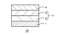
本発明の一実施の形態として、記憶素子の概略構成図(断面図)を図1に示す。
この記憶素子10は、下部電極1上にCu,Ag,Znのうちのいずれかの元素が含有された、イオン源層2が形成され、その上に記憶用薄膜3が形成され、この記憶用薄膜3上に上部電極4が形成されて構成されている。
As an embodiment of the present invention, a schematic configuration diagram (cross-sectional view) of a memory element is shown in FIG.
In this
下部電極1には、半導体プロセスに用いられる配線材料、例えばTiW,Ti,W,Cu,Al,Mo,Ta,WN,TaN,シリサイド等を用いることができる。
上部電極4には、下部電極1と同様、通常の半導体配線材料が用いられる。
For the
As with the
また、イオン源層2は、例えば、Te,Se,Sのカルコゲナイド元素を含有する、GeSbTe,GeTe,GeSe,GeS,SiGeTe,SiGeSbTe等に、Cu,Ag,Znを加えた組成の膜、Ag膜、Ag合金膜、Cu膜、Cu合金膜、Zn膜、Zn合金膜等を用いて構成することができる。
なお、このイオン源層2に、必要に応じて、Geや希土類元素等を添加することにより、耐熱性を向上することができる。
In addition, the
In addition, heat resistance can be improved by adding Ge, rare earth elements, etc. to this
記憶用薄膜3は、希土類元素と酸素とを含有する材料、例えば、酸化ガドリニウム等の希土類酸化物を用いて構成することができる。
この記憶用薄膜3は、0.5nm〜10nm程度の膜厚で形成する。
このように、記憶用薄膜3の膜厚を薄くすることにより、通常絶縁材料である希土類酸化物等から成る記憶用薄膜3に電流を流すことが可能になる。
The memory
The memory
Thus, by reducing the film thickness of the memory
上述した材料からなる記憶用薄膜3は、電圧パルス或いは電流パルスが印加されることにより、インピーダンス(抵抗値)が変化する特性を有する。
そして、この記憶用薄膜3は、他の層よりも抵抗値の変化が充分大きい。そのため、記憶素子10全体の抵抗値の変化は、主として記憶用薄膜3により影響される。
従って、記憶用薄膜3の抵抗値の変化を利用して、記憶素子10に情報の記録を行うことができる。
The memory
The memory
Therefore, information can be recorded in the
なお、図1に示す記憶素子10では、イオン源層2の上に記憶用薄膜3が形成されているが、記憶用薄膜3の上にイオン源層2を形成してもよい。
In the
本実施の形態の記憶素子10は、次のように動作させて、情報の記憶を行うことができる。
The
まず、Cu,Ag,Znが含まれたイオン源層2に接する下部電極1側が負に、上部電極4側が正になるように、記憶素子10に対して電圧を印加する。
ここで、このとき、記憶素子10に印加する電圧を、正電圧(+)と定義して、以下同様に定義して説明する。
記憶素子10への正電圧の印加により、イオン源層2からCu,Ag,Znがイオン化して、記憶用薄膜3内を拡散していき、上部電極4側で電子と結合して析出する、或いは、記憶用薄膜3内部に拡散した状態で留まる。
すると、記憶用薄膜3内部にCu,Ag,Znを多量に含む電流パスが形成される、もしくは、記憶用薄膜3内部にCu,Ag,Znによる欠陥が多数形成されることによって、記憶用薄膜3の抵抗値が低くなる。記憶用薄膜3以外の各層は、記憶用薄膜3の記録前の抵抗値に比べて、元々抵抗値が低いので、記憶用薄膜3の抵抗値を低くすることにより、記憶素子10全体の抵抗値も低くすることができる。
その後、正電圧を除去して、記憶素子10にかかる電圧をなくすと、抵抗値が低くなった状態で保持される。これにより、情報を記録することが可能になる。一度だけ記録が可能な記憶装置、いわゆる、PROMに用いる場合には、この過程(記録過程)のみで記録が完結する。
First, a voltage is applied to the
Here, the voltage applied to the
By applying a positive voltage to the
Then, a current path containing a large amount of Cu, Ag, Zn is formed inside the memory
After that, when the positive voltage is removed and the voltage applied to the
また、RAM或いはEEPROM等の記憶装置へ応用する場合には、記憶素子10を抵抗値の高い状態に戻す消去過程が必要である。
この消去過程においては、下部電極1側が正負に、上部電極4側が負になるように、記憶素子10に対して負電圧(−)を印加する。
記憶素子10への負電圧の印加により、記憶用薄膜3内に形成されていた電流パス或いは不純物準位を構成していたCu,Ag,Znがイオン化して、記憶用薄膜3内を移動してイオン源層2側に戻る。
すると、記憶用薄膜3内からCu,Ag,Znによる電流パス、もしくは、欠陥が消滅して、記憶用薄膜3の抵抗値が高くなる。記憶用薄膜3以外の各層は元々抵抗値が低いので、記憶用薄膜3の抵抗値を高くすることにより、記憶素子10全体の抵抗値も高くすることができる。
その後、負電圧を除去して、記憶素子10にかかる電圧をなくすと、抵抗値が高くなった状態で保持される。これにより、記録された情報を消去することが可能になる。
Further, when applied to a storage device such as a RAM or an EEPROM, an erasing process for returning the
In this erasing process, a negative voltage (−) is applied to the
By applying a negative voltage to the
Then, current paths or defects due to Cu, Ag, and Zn disappear from the memory
After that, when the negative voltage is removed and the voltage applied to the
このような過程を繰り返すことにより、記憶素子10に情報の記録(書き込み)と記録された情報の消去を繰り返し行うことができる。
By repeating such a process, it is possible to repeatedly record (write) information on the
そして、例えば、抵抗値の高い状態を「0」の情報に、抵抗値の低い状態を「1」の情報に、それぞれ対応させると、正電圧の印加による情報の記録過程で「0」から「1」に変え、負電圧の印加による情報の消去過程で「1」から「0」に変えることができる。
即ち、記憶素子10の抵抗値の高低により、2値の情報を記憶させることができる。
For example, if a state with a high resistance value is associated with information “0” and a state with a low resistance value is associated with information “1”, the information recording process by applying a positive voltage changes from “0” to “ It can be changed from “1” to “0” in the process of erasing information by applying a negative voltage.
That is, binary information can be stored depending on the resistance value of the
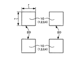
本実施の形態の記憶素子10では、特に、図2に平面図を示すように、記憶素子10の各メモリセル20の平面形状を正方形状とする。各メモリセル20の間は、絶縁層によって互いに導通しないように分離する。
さらに、正方形状のメモリセル20の一辺の長さrを、記憶素子10の「素子サイズ」と規定する。
そして、記憶素子10の素子サイズ、即ちメモリセル20の一辺の長さrを70nm以下、より好ましくは50nm以下とする。
In the
Further, the length r of one side of the
The element size of the
上述の本実施の形態の記憶素子の構成によれば、記憶素子10の素子サイズ、即ち正方形状のメモリセル20の一辺の長さrを70nm以下とすることにより、短い電圧パルスを印加して記憶素子10に書き込み(高抵抗状態から低抵抗状態に遷移させる記録動作)を行った場合の書き込み失敗を抑制して、書き込みの成功率を改善することができる。
これにより、記憶素子に情報の記録を正しく安定して行うことができる。また、短い電圧パルスによって安定して記録を行うことができるため、記録に要する時間を短縮して、記録動作の高速化を図ることができる。
According to the configuration of the memory element of the present embodiment described above, a short voltage pulse is applied by setting the element size of the
Thereby, information can be correctly and stably recorded in the storage element. In addition, since stable recording can be performed with a short voltage pulse, the time required for recording can be shortened and the recording operation can be speeded up.
さらに、記憶素子10の素子サイズ、即ち正方形状のメモリセル20の一辺の長さrを50nm以下とすることにより、記憶素子10の抵抗値のばらつき、特に抵抗値が高い消去状態の抵抗値のばらつきを、低減することが可能になる。
このように記憶素子10の抵抗値のばらつきを低減することができるため、エラーレートを小さくして、読み出し抵抗マージンを飛躍的に向上することができる。
Further, by setting the element size of the
As described above, since the variation in the resistance value of the
従って、本実施の形態によれば、記憶素子10に対して、情報の記録及び読み出しを容易に安定して行うことができる記憶素子10及び記憶装置を実現することができる。
Therefore, according to the present embodiment, it is possible to realize the
上述の実施の形態では、記憶素子10のメモリセル20の平面形状を正方形状として、正方形の一辺rを、本発明に係る素子サイズとして規定したが、メモリセルの平面形状をその他の形状とした構成にも本発明を適用することができる。
In the above-described embodiment, the planar shape of the
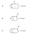
ここで、メモリセル20の平面形状を、正方形状以外の形状とした場合の、記憶素子10の素子サイズの規定箇所を、図3A〜図3Cに示す。
図3Aに示すように、メモリセル20の平面形状を長方形(矩形)とした場合には、短辺の長さSを素子サイズとして規定する。
図3Bに示すように、メモリセル20の平面形状を円形状とした場合には、直径の長さ2Rを素子サイズとして規定する。
図3Cに示すように、メモリセル20の平面形状を楕円形状とした場合には、短軸長Bを素子サイズとして規定する。
Here, when the planar shape of the
As shown in FIG. 3A, when the planar shape of the
As shown in FIG. 3B, when the planar shape of the
As shown in FIG. 3C, when the planar shape of the
なお、一般的な素子サイズとしては、その他の部分(例えば長軸や対角線の長さ等)を規定することも考えられるが、通常、各メモリセル記憶素子に接続される配線が縦横に配置され、配線と接続される電極も配線に対応して略正方形状や略矩形状とされるため、読み出し抵抗マージンに影響するパラメータとしての素子サイズは、正方形の一辺等の配線に沿った方向の寸法を規定する。
長方形状や楕円形状のような場合には、長辺又は長軸の長さよりも、短辺又は短軸の長さの方が記憶素子の抵抗値のばらつきへの影響が大きいため、短辺又は短軸の長さを素子サイズとして規定する。
In addition, as a general element size, it may be possible to define other parts (for example, the length of a major axis or diagonal line), but normally, wirings connected to each memory cell storage element are arranged vertically and horizontally. Since the electrodes connected to the wiring are also substantially square or rectangular corresponding to the wiring, the element size as a parameter affecting the read resistance margin is the dimension along the wiring such as one side of the square. Is specified.
In the case of a rectangular shape or an elliptical shape, the short side or the length of the short axis has a larger influence on the variation in the resistance value of the memory element than the length of the long side or the long axis. The length of the short axis is defined as the element size.
次に、このような構成の記憶素子10を用いた、本発明に係る記憶装置(メモリ)の実施の形態を説明する。
Next, an embodiment of a storage device (memory) according to the present invention using the
まず、本発明に係る記憶装置の一実施の形態の概略構成図(斜視図)を、図4に示す。
この記憶装置は、複数のワード線WLと、これらワード線WLと直交する複数のビット線BLとを有し、ワード線WLとビット線BLとの各交点に、図1及び図2に示したような記憶素子10(1,2,3,4)が配置されてメモリセル20が形成され、このメモリセル20が多数配置されることにより、メモリセルアレイが形成されている。図4では、3×3個のメモリセル20がマトリクス状に配列された構成のメモリセルアレイを示している。
First, FIG. 4 shows a schematic configuration diagram (perspective view) of an embodiment of a storage device according to the present invention.
This storage device has a plurality of word lines WL and a plurality of bit lines BL orthogonal to the word lines WL, and the intersections of the word lines WL and the bit lines BL are shown in FIG. 1 and FIG. Such memory elements 10 (1, 2, 3, 4) are arranged to form a
本実施の形態の記憶装置では、上述した構成(素子サイズが70nm以下である構成)の記憶素子10を用いて記憶装置を構成することにより、短い電圧パルスを印加して書き込みを行った場合の、記憶素子10の書き込み成功率が高くなることから、情報の記録を安定して行うことができる。また、短い電圧パルスによっても情報の記録を安定して行うことが可能になるため、記録動作に要する時間を短縮して、高速化を図ることができる。
また、素子サイズが50nm以下である構成の記憶素子10を用いて記憶装置を構成することにより、読み出し抵抗マージンを大きくすることができることから、読み出し時のエラーの発生が少なく、記録された情報の読み出しを安定して行うことができる。
即ち、安定して動作する、信頼性の高い記憶装置を実現することができる。
In the memory device of this embodiment, when the memory device is configured using the
In addition, by configuring the storage device using the
That is, a highly reliable storage device that operates stably can be realized.
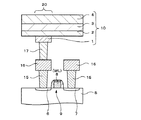
また、本発明に係る記憶装置の他の実施の形態の概略構成図(断面図)を、図5に示す。図5では、記憶装置を構成する1つの記憶素子10に対応する部分の断面構成を示している。
この記憶装置は、基板5、例えばシリコン基板上に、ソース領域6、ドレイン領域7、ゲート電極8から成るトランジスタ(MOSトランジスタ)9を有する。ゲート電極8はワード線WLを構成している。そして、ソース領域6には、プラグ層15・金属配線層16・プラグ層17を介して、図1及び図2に示した構成の記憶素子10の下部電極1が接続されている。ドレイン領域7には、プラグ層15を介して金属配線層16が接続されている。また、記憶素子10の上部電極4が、図示しないビット線BLに接続される。
そして、図5に示す構成のメモリセルを多数形成することにより、記憶装置(メモリ)が構成される。
FIG. 5 shows a schematic configuration diagram (cross-sectional view) of another embodiment of the memory device according to the present invention. FIG. 5 shows a cross-sectional configuration of a portion corresponding to one
This storage device has a transistor (MOS transistor) 9 comprising a
A memory device (memory) is configured by forming a large number of memory cells having the configuration shown in FIG.
本実施の形態の記憶装置では、下部電極1が、記憶素子10の他の層2,3,4よりも小さいパターンで形成されているため、この下部電極1のパターンによって、実際のメモリセル20の範囲が規定される。そのため、記憶素子10の素子サイズとして、下部電極1の寸法を、前述したように規定する。
例えば、下部電極1の平面形状を正方形状として、その一辺の長さrを70nm以下、より好ましくは50nm以下とする。
In the memory device according to the present embodiment, the
For example, the planar shape of the
本実施の形態の記憶装置においても、上述した構成(素子サイズが70nm以下である構成)の記憶素子10を用いて記憶装置を構成することにより、短い電圧パルスを印加して書き込みを行った場合の、記憶素子10の書き込み成功率が高くなることから、情報の記録を安定して行うことができる。また、短い電圧パルスによっても情報の記録を安定して行うことが可能になるため、記録動作に要する時間を短縮して、高速化を図ることができる。
また、素子サイズが50nm以下である構成の記憶素子10を用いて記憶装置を構成することにより、読み出し抵抗マージンを大きくすることができることから、読み出し時のエラーの発生が少なく、記録された情報の読み出しを安定して行うことができる。
即ち、安定して動作する、信頼性の高い記憶装置を実現することができる。
Also in the memory device of this embodiment, when writing is performed by applying a short voltage pulse by configuring the memory device using the
In addition, by configuring the storage device using the
That is, a highly reliable storage device that operates stably can be realized.
なお、上述した各実施の形態では、記憶素子10を構成する各層1,2,3,4をメモリセル20毎に分離した構成として説明しているが、記憶用薄膜3を含む一部の層を隣接するメモリセル20で共通に形成してもよい。ただし、下部電極1或いは上部電極4のいずれか一方は、絶縁層によりメモリセル20毎に分離する。
記憶用薄膜3が希土類元素と酸素とを有して成り、絶縁性を有するので、隣接するメモリセル20と記憶用薄膜3を共通に形成しても、導通することがない。
これにより、共通に形成した層ではパターニングの精度を高くする必要がなくなることから、素子サイズを微細化しやすくなる利点を有する。
In each of the embodiments described above, the
Since the memory
This eliminates the need to increase the patterning accuracy in the commonly formed layer, and thus has an advantage of easily miniaturizing the element size.
(実施例)
続いて、本発明の記憶素子を実際に作製して、その特性を調べた。
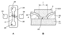
実際の記憶装置では、図4や図5に示したように、アレイ状に記憶素子を配列させていたり、記憶素子部以外にもトランジスタ等の回路素子が存在したりするが、ここでは、記憶素子の読み出し抵抗マージンを調べる目的で、図6Aに平面図、図6Bに図6AのA−A´断面図をそれぞれ示す特性評価用テストデバイス(特性評価用素子)を作製して、特性の測定・評価を行った。
(Example)
Subsequently, the memory element of the present invention was actually manufactured and its characteristics were examined.
In an actual storage device, as shown in FIGS. 4 and 5, storage elements are arranged in an array, or circuit elements such as transistors exist in addition to the storage element portion. For the purpose of examining the read resistance margin of the element, a characteristic evaluation test device (characteristic evaluation element) having a plan view in FIG. 6A and a cross-sectional view along AA ′ in FIG.・ Evaluated.
この特性評価用テストデバイスは、シリコン基板上に各メモリセルの記憶素子10に共通する下部電極1が成膜され、記憶素子のイオン源層2及び記憶用薄膜3の積層膜11が下部電極21上の絶縁層22の開口を通じて、下部電極21に接続された構成となっている。
そして、積層膜11と下部電極21とが接続された部分がメモリセル20となり、この部分の形状が図6Aに示すように正方形状となっている。
また、記憶素子の積層膜11(2,3)は、メモリセル20の周囲を含み、図6Aに示す縦長の素子形成領域23に形成されている。上部電極4は、素子形成領域23に沿って縦長に形成されている。素子形成領域23の左右に下部電極接続用端子パッド24が形成され、上部電極4の両端に上部電極接続用端子パッド25が形成されている。
In this test device for characteristic evaluation, a
The portion where the
Further, the stacked film 11 (2, 3) of the memory element includes the periphery of the
具体的には、次のようにして、図6A及び図6Bに示した特性評価用テストデバイスを作製した。
まず、厚さ2mmのシリコン基板上に下部電極21(1)として膜厚100nmのW膜を、絶縁層22としてSiO2を、順次成膜した。
その後、フォトリソグラフィを用いて、メモリセルとなる部分と下部電極接続用端子パッドとなる部分とを除く、それ以外の部分をマスクにより覆って、絶縁層22のSiO2を選択的にエッチングした。このとき、メモリセルとなる部分、即ち下部電極21上の絶縁層22の開口の平面形状を正方形状として、正方形の一辺の長さrが、それぞれ30nm,50nm,100nm,150nmである4種類の開口を、同一ウエハのシリコン基板に各種類それぞれ多数形成した。
Specifically, the test device for characteristic evaluation shown in FIGS. 6A and 6B was produced as follows.
First, a W film with a thickness of 100 nm was sequentially formed as a lower electrode 21 (1) on a 2 mm thick silicon substrate, and SiO 2 was formed as an insulating
Thereafter, by using photolithography, SiO 2 of the insulating layer 22 was selectively etched by covering the other portions except for the portion to be the memory cell and the portion to be the lower electrode connecting terminal pad with a mask. At this time, the planar shape of the opening of the insulating
次に、絶縁層22の開口を覆って、記憶素子10のイオン源層2及び記憶用薄膜3を順次成膜して、これらの積層膜11を形成した。このとき、イオン源層2としては、膜厚20nmのCuGeTeGd膜と膜厚12nmのCu膜との積層膜を形成し、記憶用薄膜3としては、希土類酸化物である酸化ガドリニウム膜を膜厚3nmで形成した。
次に、この積層膜11(2,3)に対して、フォトリソグラフィを用いて、素子形成領域23となる横200μm×縦600μmの範囲をマスクした後に、Arプラズマにより、積層膜11(2,3)をエッチングした。
さらに、上部電極4及び端子パッド24,25となる部分以外を、フォトリソグラフィを用いてマスクした後に、DCマグネトロンスパッタ法を用いて、電極材料を成膜した。そして、公知のリフトオフ法によりマスクを除去して、それぞれ電極材料から成る、上部電極4、下部電極接続用端子パッド24、上部電極接続用端子パッド25を形成した。上部電極4としては、膜厚20nmのCr膜・膜厚100nmのCu膜・膜厚100nmのAu膜の積層膜を形成した。
このようにして、正方形状のメモリセル20の一辺の長さrが、それぞれ30nm,50nm,100nm,150nmである4種類の特性評価用テストデバイスを、シリコン基板に各種類それぞれ多数作製した。
Next, the
Next, after masking a range of 200 μm × 600 μm as the
Furthermore, after masking portions other than the
In this way, a large number of four types of test devices for characteristic evaluation, each having a length r of one side of the
(特性評価)
次に、作製した特性評価用テストデバイスを用いて、記憶素子10の特性を調べた。
(Characteristic evaluation)
Next, the characteristics of the
(書き込み成功率)
正方形状のメモリセル20の一辺の長さrが異なる4種類の特性評価用テストデバイスを、各種類それぞれ72個、合計288個選び、各特性評価用テストデバイスについて、2.5Vのパルス電圧を印加して書き込みを行った。
そして、各種類の72個の特性評価用テストデバイスにおいて、書き込み動作の後の抵抗値を測定し、書き込みが成功して低抵抗状態となった素子の比率、即ち書き込み成功率を求めた。
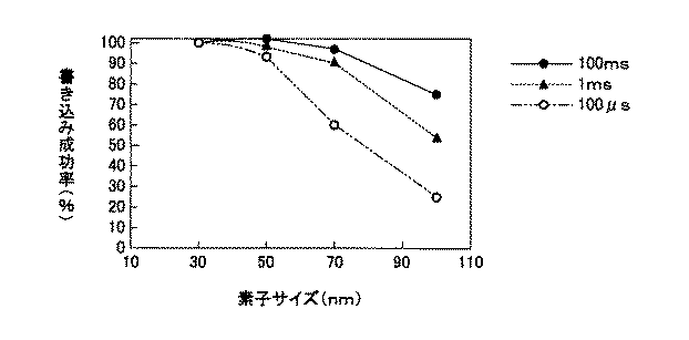
上述した方法による書き込み成功率の算出を、100m秒(100ms)、1m秒(1ms)、100μ秒(100μs)の3種類のパルス幅のパルス電圧について、それぞれ行った。
測定結果として、それぞれのパルス幅における、素子サイズ(メモリセル20の一辺の長さr)と書き込み成功率との関係を図7に示す。
(Write success rate)
Four types of characteristic evaluation test devices having different lengths r on one side of the
Then, in 72 types of test devices for characteristic evaluation, the resistance value after the write operation was measured, and the ratio of the elements in which the write was successful and the low resistance state was obtained, that is, the write success rate was obtained.
The calculation of the writing success rate by the above-described method was performed for pulse voltages having three kinds of pulse widths of 100 ms (100 ms), 1 ms (1 ms), and 100 μsec (100 μs).
As a measurement result, FIG. 7 shows the relationship between the element size (length r of one side of the memory cell 20) and the write success rate in each pulse width.
図7より、それぞれのパルス幅において、素子サイズが大きくなるほど、書き込み成功率が低下する傾向があることがわかる。
そして、パルス幅を短くして1m秒にしたときに、書き込み成功率を90%以上にするためには、素子サイズを70nm以下とする必要があることがわかる。
また、パルス幅をさらに短くして100μ秒としたときに、書き込み成功率を90%以上にするためには、素子サイズを50nm以下とする必要があることがわかる。
FIG. 7 shows that the write success rate tends to decrease as the element size increases in each pulse width.
It can be seen that when the pulse width is shortened to 1 ms, the element size needs to be 70 nm or less in order to achieve a writing success rate of 90% or more.
It can also be seen that when the pulse width is further reduced to 100 μs, the element size needs to be 50 nm or less in order to achieve a writing success rate of 90% or more.
(読み出し抵抗マージン)
正方形状のメモリセル20の一辺の長さrが異なる4種類の特性評価用テストデバイスを、各種類それぞれ120個、合計480個選び、各特性評価用テストデバイスについて、消去状態即ち高抵抗状態の抵抗値RHighと、書き込み状態即ち低抵抗状態の抵抗値RLOWとを測定した。
具体的には、高抵抗状態とした記憶素子10に書き込み閾値電圧よりも小さい読み出し電圧を印加して抵抗値を測定し、さらに書き込み電圧を印加して記憶素子10を低抵抗状態とした後に、高抵抗状態と同一の読み出し電圧を印加して抵抗値を測定した。なお、前述した書き込みの失敗が生じると、読み出し抵抗マージンを正しく算出することができないため、書き込み電圧として、パルス電圧ではなく、2.5Vの一定電圧を印加して、書き込みの失敗が生じないようにした。
そして、各種類の120個の特性評価用テストデバイスにおいて、これらの抵抗値RHigh,RLOWの平均値及び分散を求めた。
ここで、読み出し抵抗マージンを、以下の式(1)のように定義する。
(Read resistance margin)
Four types of test devices for characteristic evaluation, each having a different length r on one side of the
Specifically, after applying a read voltage smaller than the write threshold voltage to the
Then, the average value and variance of these resistance values R High and R LOW were determined in 120 test devices for characteristic evaluation of each type.
Here, the read resistance margin is defined as in the following formula (1).
Margin:読み出し抵抗マージン
Avg(RHigh):消去状態(高抵抗状態)における抵抗値の平均値
Avg(RLow):書き込み状態(低抵抗状態)における抵抗値の平均値
σ(RHigh):消去状態(高抵抗状態)における抵抗値の分散
σ(RLow):書き込み状態(低抵抗状態)における抵抗値の分散
Max{A,B}:A,Bの最大値
Margin: Read resistance margin Avg (R High ): Average value of resistance value in erased state (high resistance state) Avg (R Low ): Average value of resistance value in write state (low resistance state) σ (R High ): Erase Resistance value variance σ (R Low ) in state (high resistance state): Resistance value variance Max (A, B) in writing state (low resistance state): Maximum value of A and B
この読み出し抵抗マージンが大きいほど、高抵抗状態及び低抵抗状態の明確な分離が可能となり、読み出し時のエラーレートを低減することができる。
そして、高抵抗状態の抵抗値及び低抵抗状態の抵抗値が、いずれも正規分布であると仮定すると、読み出し抵抗マージンが6以上であれば、99%以上の動作率となる。
As the read resistance margin is larger, the high resistance state and the low resistance state can be clearly separated, and the error rate at the time of reading can be reduced.
Assuming that both the resistance value in the high resistance state and the resistance value in the low resistance state are normally distributed, if the read resistance margin is 6 or more, the operation rate is 99% or more.
各種類の特性評価用テストデバイスについて、動作マージンとして、上述した式(1)に従って、読み出し抵抗マージンを算出した。
素子サイズ(メモリセル20の一辺の長さr)と動作マージンとの関係を図8に示す。
For each type of characteristic evaluation test device, the read resistance margin was calculated as the operation margin according to the above-described equation (1).
FIG. 8 shows the relationship between the element size (the length r of one side of the memory cell 20) and the operation margin.
図8より、素子サイズ(メモリセル20の一辺の長さr)を50nm以下とすることにより、動作マージンが6以上と大きくなることがわかる。 From FIG. 8, it can be seen that when the element size (the length r of one side of the memory cell 20) is 50 nm or less, the operation margin is increased to 6 or more.
従って、素子サイズを50nm以下とすれば、動作マージンが6以下となり、高抵抗状態と低抵抗状態とを99%以上分離することができ、エラーレートの非常に小さい記憶素子となることがわかる。 Therefore, when the element size is 50 nm or less, the operation margin is 6 or less, and it is possible to separate the high resistance state and the low resistance state by 99% or more, and the memory element has a very low error rate.
以上の結果から、記憶素子の素子サイズを50nm以下とすることにより、100μ秒の短い電圧パルスを印加して書き込みを行っても、書き込み成功率を90%以上確保することができると共に、読み出しマージンを低減することができることがわかる。 From the above results, by setting the element size of the memory element to 50 nm or less, even if writing is performed by applying a short voltage pulse of 100 μsec, a writing success rate can be secured 90% or more and a reading margin can be secured. It can be seen that can be reduced.
本発明は、上述の実施の形態に限定されるものではなく、本発明の要旨を逸脱しない範囲でその他様々な構成が取り得る。 The present invention is not limited to the above-described embodiment, and various other configurations can be taken without departing from the gist of the present invention.
1 下部電極、2 イオン源層、3 記憶用薄膜、4 上部電極、5 基板、6 ソース領域、7 ドレイン領域、8 ゲート電極、9 トランジスタ、10 記憶素子、20 メモリセル、21 シリコン基板、22 絶縁層、23 素子形成領域、WL ワード線、BL ビット線
DESCRIPTION OF
Claims (4)
第2の電極と、
前記第1の電極及び前記第2の電極の間に挟まれ、酸化ガドリニウム膜から成る記憶用薄膜と、
前記第1の電極及び前記第2の電極の間に挟まれ、前記記憶用薄膜と接して設けられ、Cu,Ag,Znから選ばれるいずれかのイオンとなる元素が含まれたイオン源層とを含み、
素子の平面形状が正方形状であり、正方形の一辺の長さが50nm以下である
記憶素子。 A first electrode;
A second electrode ;
A memory thin film made of a gadolinium oxide film sandwiched between the first electrode and the second electrode ;
An ion source layer sandwiched between the first electrode and the second electrode, provided in contact with the memory thin film, and containing an element to be any ion selected from Cu, Ag, and Zn ; Including
A memory element in which the planar shape of the element is a square shape and the length of one side of the square is 50 nm or less .
前記第1の電極側に接続された配線と、
前記第2の電極側に接続された配線とを有し、
前記記憶素子が多数配置されて成る
記憶装置。 A first electrode; a second electrode ; a memory thin film comprising a gadolinium oxide film sandwiched between the first electrode and the second electrode; the first electrode and the second electrode; And an ion source layer containing an element that becomes any one of ions selected from Cu, Ag, and Zn. The planar shape of the element is a square shape. A storage element having a length of one side of a square of 50 nm or less ;
Wiring connected to the first electrode side;
A wiring connected to the second electrode side,
Memory device wherein the memory elements are arranged a number.
Priority Applications (1)
| Application Number | Priority Date | Filing Date | Title |
|---|---|---|---|
| JP2005208912A JP4635759B2 (en) | 2005-07-19 | 2005-07-19 | Storage element and storage device |
Applications Claiming Priority (1)
| Application Number | Priority Date | Filing Date | Title |
|---|---|---|---|
| JP2005208912A JP4635759B2 (en) | 2005-07-19 | 2005-07-19 | Storage element and storage device |
Publications (2)
| Publication Number | Publication Date |
|---|---|
| JP2007027499A JP2007027499A (en) | 2007-02-01 |
| JP4635759B2 true JP4635759B2 (en) | 2011-02-23 |
Family
ID=37787854
Family Applications (1)
| Application Number | Title | Priority Date | Filing Date |
|---|---|---|---|
| JP2005208912A Expired - Fee Related JP4635759B2 (en) | 2005-07-19 | 2005-07-19 | Storage element and storage device |
Country Status (1)
| Country | Link |
|---|---|
| JP (1) | JP4635759B2 (en) |
Families Citing this family (1)
| Publication number | Priority date | Publication date | Assignee | Title |
|---|---|---|---|---|
| JP5194667B2 (en) * | 2007-09-14 | 2013-05-08 | ソニー株式会社 | Variable resistance element and memory device |
Family Cites Families (5)
| Publication number | Priority date | Publication date | Assignee | Title |
|---|---|---|---|---|
| US6418049B1 (en) * | 1997-12-04 | 2002-07-09 | Arizona Board Of Regents | Programmable sub-surface aggregating metallization structure and method of making same |
| AU763809B2 (en) * | 1999-02-11 | 2003-07-31 | Arizona Board Of Regents On Behalf Of The University Of Arizona, The | Programmable microelectronic devices and methods of forming and programming same |
| US6693821B2 (en) * | 2001-06-28 | 2004-02-17 | Sharp Laboratories Of America, Inc. | Low cross-talk electrically programmable resistance cross point memory |
| US7750332B2 (en) * | 2002-04-30 | 2010-07-06 | Japan Science And Technology Agency | Solid electrolyte switching device, FPGA using same, memory device, and method for manufacturing solid electrolyte switching device |
| JP2005167064A (en) * | 2003-12-04 | 2005-06-23 | Sharp Corp | Nonvolatile semiconductor memory device |
-
2005
- 2005-07-19 JP JP2005208912A patent/JP4635759B2/en not_active Expired - Fee Related
Also Published As
| Publication number | Publication date |
|---|---|
| JP2007027499A (en) | 2007-02-01 |
Similar Documents
| Publication | Publication Date | Title |
|---|---|---|
| JP4529654B2 (en) | Storage element and storage device | |
| JP4848633B2 (en) | Storage element and storage device | |
| US9767899B2 (en) | Access signal conditioning for memory cells in an array | |
| US7145791B2 (en) | Memory device having variable resistive memory element | |
| JP4396621B2 (en) | Storage element and storage device | |
| US20090224224A1 (en) | Nonvolatile memory element, nonvolatile memory apparatus, nonvolatile semiconductor apparatus, and method of manufacturing nonvolatile memory element | |
| US8148711B2 (en) | Nonvolatile memory element, manufacturing method thereof, and nonvolatile semiconductor apparatus using nonvolatile memory element | |
| JP2009141225A (en) | Variable resistance element, variable resistance element manufacturing method, and nonvolatile semiconductor memory device | |
| JP2006040946A (en) | Memory element | |
| JPWO2007023569A1 (en) | Nonvolatile semiconductor memory device and writing method thereof | |
| JP2012128892A (en) | Memory device | |
| JP4465969B2 (en) | Semiconductor memory element and semiconductor memory device using the same | |
| CN100524510C (en) | Storage and semiconductor device | |
| CN111668367B (en) | storage device | |
| JP5007502B2 (en) | Method for manufacturing memory element | |
| JP5194640B2 (en) | Storage element and storage device | |
| JP4742971B2 (en) | Storage element and storage device | |
| JP4635759B2 (en) | Storage element and storage device | |
| JP4816314B2 (en) | Storage element and storage device | |
| JP5257573B2 (en) | Storage element and storage device | |
| JP4760606B2 (en) | Storage element and storage device | |
| JP4552752B2 (en) | Storage element manufacturing method and storage device manufacturing method | |
| JP2007157941A (en) | Storage element and storage device | |
| JP5360145B2 (en) | Storage element and storage device | |
| JP5423940B2 (en) | Storage element manufacturing method and storage device manufacturing method |
Legal Events
| Date | Code | Title | Description |
|---|---|---|---|
| A621 | Written request for application examination |
Free format text: JAPANESE INTERMEDIATE CODE: A621 Effective date: 20080609 |
|
| A977 | Report on retrieval |
Free format text: JAPANESE INTERMEDIATE CODE: A971007 Effective date: 20100805 |
|
| A131 | Notification of reasons for refusal |
Free format text: JAPANESE INTERMEDIATE CODE: A131 Effective date: 20100817 |
|
| A521 | Request for written amendment filed |
Free format text: JAPANESE INTERMEDIATE CODE: A523 Effective date: 20101006 |
|
| TRDD | Decision of grant or rejection written | ||
| A01 | Written decision to grant a patent or to grant a registration (utility model) |
Free format text: JAPANESE INTERMEDIATE CODE: A01 Effective date: 20101026 |
|
| A01 | Written decision to grant a patent or to grant a registration (utility model) |
Free format text: JAPANESE INTERMEDIATE CODE: A01 |
|
| A61 | First payment of annual fees (during grant procedure) |
Free format text: JAPANESE INTERMEDIATE CODE: A61 Effective date: 20101108 |
|
| FPAY | Renewal fee payment (event date is renewal date of database) |
Free format text: PAYMENT UNTIL: 20131203 Year of fee payment: 3 |
|
| FPAY | Renewal fee payment (event date is renewal date of database) |
Free format text: PAYMENT UNTIL: 20131203 Year of fee payment: 3 |
|
| LAPS | Cancellation because of no payment of annual fees |