JP4540968B2 - Plasma display panel manufacturing method and plasma display - Google Patents
Plasma display panel manufacturing method and plasma display Download PDFInfo
- Publication number
- JP4540968B2 JP4540968B2 JP2003383610A JP2003383610A JP4540968B2 JP 4540968 B2 JP4540968 B2 JP 4540968B2 JP 2003383610 A JP2003383610 A JP 2003383610A JP 2003383610 A JP2003383610 A JP 2003383610A JP 4540968 B2 JP4540968 B2 JP 4540968B2
- Authority
- JP
- Japan
- Prior art keywords
- plasma display
- photosensitive
- weight
- oxide
- layer
- Prior art date
- Legal status (The legal status is an assumption and is not a legal conclusion. Google has not performed a legal analysis and makes no representation as to the accuracy of the status listed.)
- Expired - Fee Related
Links
Images


Description
本発明は、壁掛けテレビや大型モニターに用いられるプラズマディスプレイ用部材の製造方法に係り、特に、プラズマディスプレイパネルの輝度を向上し、パネルの表示品位を高めたプラズマディスプレイ用部材の製造方法並びにプラズマディスプレイに関するものである。 The present invention relates to a method of manufacturing a member for a plasma display used for a wall-mounted television or a large monitor, and more particularly, a method for manufacturing a member for a plasma display with improved brightness and improved display quality of the plasma display panel, and a plasma display It is about.
薄型・大型テレビに使用できるディスプレイとして、プラズマディスプレイパネル(以下、PDPと略す)が注目されている。PDPは、例えば、表示面となる前面板側のガラス基板には、対をなす複数のサステイン電極が銀やクロム、アルミニウムおよびニッケル等の材料で形成されている。 A plasma display panel (hereinafter abbreviated as PDP) has attracted attention as a display that can be used for thin and large televisions. In the PDP, for example, a plurality of paired sustain electrodes are formed of a material such as silver, chromium, aluminum, and nickel on a glass substrate on a front plate side that serves as a display surface.
また、PDPの発光画素間に相当する部位に、コントラスト等の表示品位を向上させる目的で、ブラックストライプパターンが形成されている。 In addition, a black stripe pattern is formed in a portion corresponding to the light emitting pixels of the PDP for the purpose of improving display quality such as contrast.
さらにサステイン電極、ブラックストライプパターンを被覆してガラスを主成分とする誘電体層が20〜50μm厚さで形成され、その誘電体層を被覆してMgO層が形成されている。一方、背面板側のガラス基板には、複数のアドレス電極がストライプ状に形成され、そのアドレス電極を被覆してガラスを主成分とする誘電体層が形成されている。誘電体層上に放電セルを仕切るための隔壁が形成され、隔壁と誘電体層で形成された放電空間内に蛍光体層が形成されている。フルカラー表示が可能なPDPにおいては、蛍光体層は、赤緑青(RGB)の各色に発光するものにより構成される。前面板側のガラス基板のサステイン電極と背面板側のアドレス電極が互いに直交するように、前面板と背面板が封着され、それらの基板の間隙内にヘリウム、ネオンおよびキセノンなどから構成される希ガスが封入されPDPが形成される。スキャン電極とアドレス電極の交点を中心として画素セルが形成されるので、PDPは複数の画素セルを有し、画像の表示が可能になる。 Further, a dielectric layer mainly composed of glass is formed with a thickness of 20 to 50 μm by covering the sustain electrode and the black stripe pattern, and an MgO layer is formed by covering the dielectric layer. On the other hand, on the glass substrate on the back plate side, a plurality of address electrodes are formed in stripes, and a dielectric layer mainly composed of glass is formed by covering the address electrodes. A partition for partitioning the discharge cells is formed on the dielectric layer, and a phosphor layer is formed in a discharge space formed by the partition and the dielectric layer. In a PDP capable of full color display, the phosphor layer is configured to emit light in red, green, and blue (RGB) colors. The front plate and the back plate are sealed so that the sustain electrode of the glass substrate on the front plate side and the address electrode on the back plate side are orthogonal to each other, and helium, neon, xenon, etc. are formed in the gap between the substrates. A rare gas is enclosed to form a PDP. Since the pixel cell is formed around the intersection of the scan electrode and the address electrode, the PDP has a plurality of pixel cells and can display an image.
PDPにおいて表示を行う際、選択された画素セルにおいて、発光していない状態からサステイン電極とアドレス電極との間に放電開始電圧以上の電圧を印加すると電離によって生じた陽イオンや電子は、画素セルが容量性負荷であるために放電空間内を反対極性の電極へと向けて移動してMgO層の内壁に帯電し、内壁の電荷はMgO層の抵抗が高いために減衰せずに壁電荷として残留する。 When a display is performed in the PDP, when a voltage higher than the discharge start voltage is applied between the sustain electrode and the address electrode from the non-lighted state in the selected pixel cell, positive ions and electrons generated by ionization are Is a capacitive load and moves toward the opposite polarity electrode in the discharge space and charges the inner wall of the MgO layer. The inner wall charge is not attenuated due to the high resistance of the MgO layer, and becomes a wall charge. Remains.
次に、スキャン電極とサステイン電極の間に放電維持電圧を印加する。壁電荷のあるところでは、放電開始電圧より低い電圧でも放電することができる。放電により放電空間内のキセノンガスが励起され、147nmの紫外線が発生し、紫外線が蛍光体を励起することにより、発光表示が可能になる。 Next, a sustaining voltage is applied between the scan electrode and the sustain electrode. Where there is a wall charge, it can be discharged even at a voltage lower than the discharge start voltage. The xenon gas in the discharge space is excited by the discharge, and ultraviolet light having a wavelength of 147 nm is generated. The ultraviolet light excites the phosphor, thereby enabling light emission display.
このようなPDPにおいては、蛍光面を発光させた場合の輝度を高めることが重要となっている。この輝度を高めるための手段として、隔壁と平行で隔壁よりも低い壁状の突起部や隔壁と交差する方向に隔壁よりも低い壁状の突起部を形成し、これら壁状の突起部にも蛍光面を形成することにより蛍光面の発光面積を大きくし、紫外線を効率よく蛍光面に作用させ、輝度を高めることが提案されている(特許文献1参照)。 In such a PDP, it is important to increase the luminance when the phosphor screen emits light. As means for increasing the brightness, wall-like projections that are parallel to the partition walls and lower than the partition walls and wall-like projections that are lower than the partition walls are formed in the direction intersecting the partition walls. It has been proposed to increase the luminance by increasing the light emitting area of the phosphor screen by forming the phosphor screen and allowing the ultraviolet rays to efficiently act on the phosphor screen (see Patent Document 1).
この隔壁と壁状の突起部の形成方法として特許文献1には、2回塗布/2回露光する方法、例えば、基板上に第1の感光性隔壁材料層を形成し、その上に壁状の突起部のパターンを有するフォトマスクを配置して露光を行い、そのまま現像せずに第1の感光性隔壁材料層上に第2の感光性隔壁材料層を形成し、その上に隔壁のパターンを有するフォトマスクを配置して露光を行った後に現像し、壁状の突起部と隔壁を形成する方法が提案されている。 As a method for forming the partition walls and the wall-shaped protrusions, Patent Document 1 discloses a method of applying twice / exposing twice, for example, forming a first photosensitive partition material layer on a substrate, and forming a wall shape thereon. A photomask having a pattern of protrusions is placed for exposure, and the second photosensitive barrier rib material layer is formed on the first photosensitive barrier rib material layer without developing as it is, and the barrier rib pattern is formed thereon. There has been proposed a method of forming a wall-shaped protrusion and a partition wall by arranging a photomask having a mask and developing it after exposure.
しかしながら、この方法では、第1の感光性隔壁材料層と第2の感光性隔壁材料層の塗布幅が同じになった場合、あるいは第1の感光性隔壁層の塗布幅の方が広い場合、焼成後に隔壁パターンが第1の感光性隔壁材料層と第2の感光性隔壁材料層の界面で剥離したり、パターン端部が跳ね上がり、パネル化した際にこの部分に色のクロストークが発生し、高品質なプラズマディスプレイパネルができない問題が生じていた。 However, in this method, when the application width of the first photosensitive barrier rib material layer and the second photosensitive barrier rib material layer are the same, or when the application width of the first photosensitive barrier rib layer is wider, After firing, the barrier rib pattern peels off at the interface between the first photosensitive barrier rib material layer and the second photosensitive barrier rib material layer, or when the pattern edge jumps up and forms a panel, color crosstalk occurs in this portion. There was a problem that a high-quality plasma display panel could not be made.
また、フォトマスクの傷やフォトマスクに付着した異物のために隔壁パターンに欠陥が生じ、パネル化した際に放電の干渉や色のクロストークが発生し、パネルの収率を低下させ、プラズマディスプレイパネルの製造コストを上げる原因にもなっていた。
そこで、本発明は、跳ね上がりやパターン欠陥のない隔壁パターンを形成し、表示品位に優れたプラズマプラズマディスプレイパネルの製造方法、およびプラズマディスプレイを低コストで提供することを目的とするものである。
SUMMARY OF THE INVENTION Accordingly, an object of the present invention is to provide a plasma plasma display panel manufacturing method and a plasma display at low cost by forming a barrier rib pattern free from jumping and pattern defects and having excellent display quality.
すなわち本発明は、隔壁を形成する工程を含むプラズマディスプレイパネルの製造方法であって、前記隔壁のパターンを形成する工程が下記の(A)〜(F)の工程を順に経ることを特徴とするプラズマディスプレイパネルの製造方法である。
(A)前記隔壁の一部となる1層目のパターン形成用感光性塗布膜を形成する工程、
(B)前記1層目のパターン形成用感光性塗布膜を第1のフォトマスクを介して露光する工程、
(C)前記隔壁の一部となる2層目のパターン形成用感光性塗布膜を前記1層目のパターン形成用感光性塗布膜幅よりも広く形成する工程、
(D)前記2層目のパターン形成用感光性塗布膜を第2のフォトマスクを介して露光する工程、
(E)現像する工程、
(F)焼成する工程。
That is, the present invention is a method for manufacturing a plasma display panel including a step of forming a barrier rib , wherein the step of forming the pattern of the barrier ribs includes the following steps (A) to (F) in order. It is a manufacturing method of a plasma display panel .
(A) a step of forming a first-layer pattern-forming photosensitive coating film that becomes a part of the partition ;
(B) exposing the first layer pattern forming photosensitive coating film through a first photomask;
(C) forming a second layer pattern forming photosensitive coating film, which is a part of the partition wall, wider than the first layer pattern forming photosensitive coating film;
(D) exposing the second layer pattern-forming photosensitive coating film through a second photomask;
(E) developing step,
(F) A step of firing.
また、本発明のプラズマデイスプレイパネルの製造方法は、次の好ましい態様を有している。
(a) 前記第2のフォトマスクの線幅が前記第1 のフォトマスクの線幅より広いこと。
(b) 前記感光性塗布膜が感光性隔壁ペーストにより形成されること。
(c) 前記感光性塗布膜がダイコーターにより形成されること。
Moreover, the manufacturing method of the plasma display panel of this invention has the following preferable aspects.
(a) The line width of the second photomask is wider than the line width of the first photomask.
(b) The photosensitive coating film is formed of a photosensitive partition paste.
(c) The photosensitive coating film is formed by a die coater.
また、本発明のプラズマプラズマディスプレイは、上記の製造方法で得られたプラズマディスプレイパネルを用いてなることを特徴とする。
The plasma plasma display of the present invention, characterized by using a plasma display panel obtained by the above-described manufacturing method.
本発明によれば、跳ね上がりやパターン欠陥のない隔壁を形成し、表示品位に優れたプラズマディスプレイを提供することができるプラズマディスプレイパネルを得ることができる。 ADVANTAGE OF THE INVENTION According to this invention, the plasma display panel which can form the partition without a jump and a pattern defect, and can provide the plasma display excellent in the display quality can be obtained.
以下、本発明のプラズマディスプレイ用部材とプラズマディスプレイを、PDPの作製手順に沿って説明する。 Hereinafter, the member for a plasma display and the plasma display of the present invention will be described in accordance with a procedure for producing a PDP.
本発明で用いられる基板としては、ソーダガラス板の他にPDP用の耐熱ガラス板である旭硝子社製の“PD200”や日本電気硝子社製の“PP8”などのガラス基板を用いることができる。 As the substrate used in the present invention, a glass substrate such as “PD200” manufactured by Asahi Glass Co., Ltd. or “PP8” manufactured by Nippon Electric Glass Co., Ltd., which is a heat-resistant glass plate for PDP, can be used in addition to the soda glass plate.
ガラス基板上に、銀、アルミニウム、クロムおよびニッケルなどの金属によりアドレス電極を形成する。アドレス電極を形成する方法としては、これらの金属の粉末と有機バインダーを主成分とする金属ペーストをスクリーン印刷でパターン印刷する方法や、有機バインダーとして感光性有機成分を用いた感光性金属ペーストを塗布した後に、フォトマスクを用いてパターン露光し、不要な部分を現像工程で溶解除去し、さらに、400〜600℃の温度に加熱・焼成して金属パターンを形成する感光性ペースト法を用いることができる。また、ガラス基板上に、クロムやアルミニウム等の金属をスパッタリングした後に、レジストを塗布し、レジストをパターン露光・現像した後に、エッチングにより不要な部分の金属を取り除くエッチング法を用いることができる。 An address electrode is formed on a glass substrate with a metal such as silver, aluminum, chromium and nickel. As a method of forming the address electrode, a metal paste mainly composed of these metal powders and an organic binder is printed by screen printing, or a photosensitive metal paste using a photosensitive organic component as an organic binder is applied. After that, a photosensitive paste method is used in which pattern exposure is performed using a photomask, unnecessary portions are dissolved and removed in a development step, and further, a metal pattern is formed by heating and baking to a temperature of 400 to 600 ° C. it can. Further, after sputtering a metal such as chromium or aluminum on a glass substrate, a resist is applied, and after the resist is subjected to pattern exposure / development, an etching method in which unnecessary portions of metal are removed by etching can be used.
電極の厚さは1〜10μmが好ましく、より好ましくは2〜5μmである。電極厚さが薄すぎると抵抗値が大きくなり正確な駆動が困難となる傾向にあり、厚すぎると材料が多く必要になり、コスト的に不利な傾向にある。アドレス電極の幅は、好ましくは20〜200μmであり、より好ましくは30〜100μmである。アドレス電極の幅が細すぎると抵抗値が高くなり正確な駆動が困難となる傾向にあり、また、太すぎると隣合う電極間の距離が小さくなるため、ショート欠陥が生じやすい傾向にある。さらに、アドレス電極は表示セル(画素の各RGBを形成する領域)に応じたピッチで形成される。通常のPDPでは100〜500μm、高精細PDPにおいては100〜400μmのピッチで形成することが好ましい。 The thickness of the electrode is preferably 1 to 10 μm, more preferably 2 to 5 μm. If the electrode thickness is too thin, the resistance value tends to increase and accurate driving tends to be difficult. The width of the address electrode is preferably 20 to 200 μm, more preferably 30 to 100 μm. If the width of the address electrode is too thin, the resistance value tends to be high and accurate driving tends to be difficult. If it is too thick, the distance between adjacent electrodes tends to be small, so that a short defect tends to occur. Further, the address electrodes are formed at a pitch corresponding to the display cell (region where each RGB of the pixel is formed). A normal PDP is preferably formed at a pitch of 100 to 500 μm, and a high-definition PDP is preferably formed at a pitch of 100 to 400 μm.
次いで、誘電体層を好ましく形成する。誘電体層は、ガラス粉末と有機バインダーを主成分とするガラスペーストをアドレス電極を覆う形で塗布した後に、400〜600℃の温度で焼成することにより形成することができる。誘電体層に用いられるガラスペーストには、酸化鉛、酸化ビスマス、酸化亜鉛および酸化リンの少なくとも1種類以上を含有し、これらを合計で10〜80重量%含有するガラス粉末を好ましく用いることができる。ガラス粉末の量を10重量%以上とすることで、600℃以下の温度での焼成が容易になり、80重量%以下とすることで、結晶化を防ぎ透過率の低下を防止する。これらのガラス粉末と有機バインダーと混練してペーストを作成できる。用いられる有機バインダーとしては、例えば、エチルセルロース、メチルセルロース等に代表されるセルロース系化合物、メチルメタクリレート、エチルメタクリレート、イソブチルメタクリレート、メチルアクリレート、エチルアクリレートおよびイソブチルアクリレート等のアクリル系化合物等を用いることができる。 Next, a dielectric layer is preferably formed. The dielectric layer can be formed by applying a glass paste containing glass powder and an organic binder as main components so as to cover the address electrodes, and then baking at a temperature of 400 to 600 ° C. For the glass paste used for the dielectric layer, glass powder containing at least one kind of lead oxide, bismuth oxide, zinc oxide and phosphorus oxide and containing 10 to 80% by weight in total can be preferably used. . By making the amount of the glass powder 10% by weight or more, firing at a temperature of 600 ° C. or less is facilitated, and by making it 80% by weight or less, crystallization is prevented and a decrease in transmittance is prevented. A paste can be prepared by kneading these glass powder and an organic binder. Examples of organic binders that can be used include cellulose compounds such as ethyl cellulose and methyl cellulose, and acrylic compounds such as methyl methacrylate, ethyl methacrylate, isobutyl methacrylate, methyl acrylate, ethyl acrylate, and isobutyl acrylate.
また、ガラスペースト中に、溶媒や可塑剤等の添加剤を加えても良い。溶媒としては、テルピネオール、ブチロラクトン、トルエンおよびメチルセルソルブ等の汎用溶媒を用いることができる。また、可塑剤としては、ジブチルフタレートやジエチルフタレート等を用いることができる。ガラス粉末以外にフィラー成分を添加することにより、反射率が高く、輝度の高いPDPを得ることができる。フィラーとしては、酸化チタン、酸化アルミニウムおよび酸化ジルコニウム等が好ましく、粒子径0.05〜3μmの酸化チタンを用いることが特に好ましい。フィラーの含有量は、ガラス粉末:フィラーの比で、1:1〜10:1の範囲が好ましい。フィラーの含有量をガラス粉末の10分の1以上とすることで、輝度向上の実効を得ることができる。また、ガラス粉末の等量以下とすることで、焼結性を保つことができる。また、導電性微粒子を添加することにより駆動時の信頼性の高いPDPを作成することができる。導電性微粒子は、ニッケルやクロムなどの金属粉末が好ましく、粒子径は1〜10μmの範囲のものが好ましい。粒子径を1μm以上とすることで十分な効果を発揮することができ、10μm以下とすることで誘電体上の凹凸を抑え隔壁形成を容易にすることができる。これらの導電性微粒子が誘電体層に含まれる含有量としては、0.1〜10重量%が好ましい。含有量を0.1重量%以上とすることで実効を得ることができ、10重量%以下とすることで、隣り合うアドレス電極間でのショートを防ぐことができる。誘電体層の厚さは、好ましくは3〜30μmであり、より好ましくは3〜15μmである。誘電体層の厚さが薄すぎるとピンホールが多発する傾向にあり、厚すぎると放電電圧が高くなり、消費電力が大きくなる傾向にある。 Moreover, you may add additives, such as a solvent and a plasticizer, in glass paste. As the solvent, general-purpose solvents such as terpineol, butyrolactone, toluene and methyl cellosolve can be used. As the plasticizer, dibutyl phthalate, diethyl phthalate, or the like can be used. By adding a filler component in addition to the glass powder, a PDP having a high reflectance and a high luminance can be obtained. As the filler, titanium oxide, aluminum oxide, zirconium oxide and the like are preferable, and it is particularly preferable to use titanium oxide having a particle diameter of 0.05 to 3 μm. The filler content is preferably in the range of 1: 1 to 10: 1 in the ratio of glass powder: filler. The brightness improvement effect can be obtained by setting the filler content to 1/10 or more of the glass powder. Moreover, sinterability can be maintained by setting it as below equal amount of glass powder. Further, by adding conductive fine particles, a PDP with high reliability during driving can be created. The conductive fine particles are preferably metal powders such as nickel and chromium, and those having a particle diameter in the range of 1 to 10 μm are preferable. By setting the particle diameter to 1 μm or more, a sufficient effect can be exhibited, and by setting the particle diameter to 10 μm or less, unevenness on the dielectric can be suppressed and partition formation can be facilitated. The content of these conductive fine particles contained in the dielectric layer is preferably 0.1 to 10% by weight. Effectiveness can be obtained by setting the content to 0.1% by weight or more, and shorting between adjacent address electrodes can be prevented by setting the content to 10% by weight or less. The thickness of the dielectric layer is preferably 3 to 30 μm, more preferably 3 to 15 μm. If the thickness of the dielectric layer is too thin, pinholes tend to occur frequently, and if it is too thick, the discharge voltage tends to increase and the power consumption tends to increase.
誘電体層上に、放電セルを仕切るための隔壁や輝度向上のための壁状の突起部を形成する。隔壁の断面形状は、台形や矩形に形成することができる。隔壁の高さは、80μm〜200μmが適している。隔壁の高さを80μm以上とすることで蛍光体とスキャン電極が近づきすぎるのを防ぎ、放電による蛍光体の劣化を防ぐことができる。また、隔壁の高さを200μm以下とすることで、スキャン電極での放電と蛍光体の距離を近づけ、十分な輝度を得ることができる。 On the dielectric layer, partition walls for partitioning the discharge cells and wall-shaped protrusions for improving luminance are formed. The cross-sectional shape of the partition wall can be formed as a trapezoid or a rectangle. The height of the partition wall is suitably 80 μm to 200 μm. By setting the height of the partition wall to 80 μm or more, it is possible to prevent the phosphor and the scan electrode from being too close to each other and to prevent the phosphor from being deteriorated due to discharge. In addition, by setting the height of the partition wall to 200 μm or less, it is possible to reduce the distance between the discharge at the scan electrode and the phosphor and obtain sufficient luminance.
隔壁のピッチ(P)は、100μm≦P≦500μmのものがよく用いられる。また、高精細プラズマディスプレイの隔壁のピッチ(P)は、好ましくは100μm≦P≦250μmである。隔壁のピッチ(P)を100μm以上とすることで放電空間を広くし十分な輝度を得ることができ、500μm以下とすることで画素の細かいきれいな映像表示ができる。隔壁のピッチ(P)を250μm以下にすることにより、HDTV(ハイビジョン)レベルの美しい映像を表示することができる。 The partition pitch (P) is often 100 μm ≦ P ≦ 500 μm. The pitch (P) of the partition walls of the high-definition plasma display is preferably 100 μm ≦ P ≦ 250 μm. By setting the partition pitch (P) to 100 μm or more, the discharge space can be widened and sufficient luminance can be obtained, and by setting the pitch to 500 μm or less, a fine image with fine pixels can be displayed. By setting the pitch (P) of the partition walls to 250 μm or less, it is possible to display a beautiful video of HDTV (high vision) level.
線幅(L)は、半値幅で10μm≦L≦50μmであることが好ましい。線幅(L)を10μm以上とすることで強度を保ち、前面板と背面板を封着する際に破損が生じることを防ぐことができ、また、50μm以下とすることで蛍光体の形成面積を大きくとることができ高い輝度を得ることができる。 The line width (L) is preferably 10 μm ≦ L ≦ 50 μm in half width. By maintaining the line width (L) to 10 μm or more, the strength can be maintained, and it is possible to prevent breakage when sealing the front plate and the back plate. Can be made large, and high luminance can be obtained.
本発明では、壁状の突起部はなくてもよいが、壁状の突起部を形成することで、輝度が向上できるため壁状の突起部を形成するこが好ましい。壁状の突起部を形成することで、壁状の突起部にも蛍光体層を形成することができ、発光面積を大きくとることができる。従って、紫外線が効率よく蛍光面に作用するため輝度を高めることが可能である。また、補助隔壁が存在することで、隔壁全体の結合面積が広くなり、部材の構造的強度が得られる。その結果、隔壁や補助隔壁の幅を小さくすることができ、表示セル部における放電容積を大きくすることができ、放電効率をさらによくすることができる。 In the present invention, there is no need for the wall-shaped protrusion, but it is preferable to form the wall-shaped protrusion because the luminance can be improved by forming the wall-shaped protrusion. By forming the wall-shaped protrusions, the phosphor layer can be formed also on the wall-shaped protrusions, and the light emission area can be increased. Accordingly, it is possible to increase the luminance because the ultraviolet rays efficiently act on the phosphor screen. Further, the presence of the auxiliary partition wall increases the bonding area of the entire partition wall, and the structural strength of the member can be obtained. As a result, the width of the barrier ribs and auxiliary barrier ribs can be reduced, the discharge volume in the display cell portion can be increased, and the discharge efficiency can be further improved.
壁状の突起部は、隔壁と平行あるいは隔壁と交差する方向に設けられてもよいが、隔壁より低く形成することが好ましい。壁状の突起部を隔壁より低く形成することで、製造工程において蛍光体層の形成を容易にすることができる利点や前面板と封着した後の封排気が容易になる利点がある。 The wall-shaped protrusions may be provided in a direction parallel to or intersecting the partition walls, but are preferably formed lower than the partition walls. By forming the wall-shaped protrusions lower than the partition walls, there are advantages that the phosphor layer can be easily formed in the manufacturing process and that sealing and exhausting after sealing with the front plate is facilitated.
このような隔壁および壁状の突起部は、無機微粒子と感光性有機成分からなる感光性ペーストを用いてパターン形成した後に、焼成して形成することができる。 Such partition walls and wall-shaped protrusions can be formed by baking after forming a pattern using a photosensitive paste comprising inorganic fine particles and a photosensitive organic component.
感光性ペーストの無機微粒子としては、ガラスやセラミック(アルミナ、コーディライトなど)などを用いることができる。特に、ケイ素酸化物、ホウ素酸化物またはアルミニウム酸化物を必須成分とするガラスやセラミックスが好ましい。 As the inorganic fine particles of the photosensitive paste, glass, ceramic (alumina, cordierite, etc.) and the like can be used. In particular, glass or ceramics containing silicon oxide, boron oxide or aluminum oxide as an essential component is preferable.
無機微粒子の粒子径は、作製しようとするパターンの形状を考慮して選ばれるが、体積平均粒子径(D50)が、1〜10μmであることが好ましく、より好ましくは1〜5μmである。D50を10μm以下とすることで、表面凸凹が生じるのを防ぐことができる。また、D50を1μm以上とすることで、ペーストの粘度調整を容易にすることができる。さらに、パターン形成において、比表面積0.2〜3m2/gのガラス微粒子を用いることが、特に好ましい。 The particle diameter of the inorganic fine particles is selected in consideration of the shape of the pattern to be produced, but the volume average particle diameter (D50) is preferably 1 to 10 μm, more preferably 1 to 5 μm. By setting D50 to 10 μm or less, it is possible to prevent surface irregularities from occurring. Moreover, the viscosity adjustment of a paste can be made easy by D50 being 1 micrometer or more. Furthermore, in pattern formation, it is particularly preferable to use glass fine particles having a specific surface area of 0.2 to 3 m 2 / g.
隔壁および壁状の突起部は、好ましくは熱軟化点の低いガラス基板上にパターン形成されるため、無機微粒子として、熱軟化温度が350℃〜600℃のガラス微粒子を60重量%以上含む無機微粒子を用いることが好ましい。また、熱軟化温度が600℃以上のガラス微粒子やセラミック微粒子を添加することによって、焼成時の収縮率を抑制することができるが、その量は、40重量%以下であることが好ましい。用いられるガラス粉末としては、焼成時にガラス基板にそりを生じさせないためには線膨脹係数が50×10-7〜90×10-7、更には、60×10-7〜90×10-7のガラス微粒子を用いることが好ましい。 Since the partition walls and the wall-shaped protrusions are preferably patterned on a glass substrate having a low thermal softening point, the inorganic fine particles include 60% by weight or more of glass fine particles having a thermal softening temperature of 350 ° C. to 600 ° C. as inorganic fine particles. Is preferably used. Further, by adding glass fine particles or ceramic fine particles having a heat softening temperature of 600 ° C. or higher, the shrinkage rate during firing can be suppressed, but the amount is preferably 40% by weight or less. The glass powder used has a linear expansion coefficient of 50 × 10 −7 to 90 × 10 −7 , and further 60 × 10 −7 to 90 × 10 −7 so as not to cause warpage of the glass substrate during firing. It is preferable to use glass fine particles.
隔壁および壁状の突起部を形成する素材としては、ケイ素および/またはホウ素の酸化物を含有したガラス材料が好ましく用いられる。 A glass material containing an oxide of silicon and / or boron is preferably used as a material for forming the partition walls and the wall-like protrusions.
酸化ケイ素は、3〜60重量%の範囲で配合されていることが好ましい。酸化ケイ素の配合量を3重量%以上とすることで、ガラス層の緻密性、強度や安定性が向上し、また、熱膨脹係数を所望の範囲内とし、ガラス基板とのミスマッチを防ぐことができる。また、配合量を60重量%以下にすることによって、熱軟化点が低くなり、ガラス基板への焼き付けが可能になるなどの利点がある。
It is preferable that silicon oxide is blended in the range of 3 to 60% by weight. By making the compounding amount of
酸化ホウ素は、例えば5〜50重量%の範囲で配合することによって、電気絶縁性、強度、熱膨脹係数および絶縁層の緻密性などの電気、機械および熱的特性を向上することができる。50重量%以下とすることでガラスの安定性を保つことができる。 Boron oxide can improve electrical, mechanical, and thermal characteristics such as electrical insulation, strength, thermal expansion coefficient, and denseness of the insulating layer by blending, for example, in the range of 5 to 50% by weight. The stability of glass can be maintained by setting it as 50 weight% or less.
さらに、酸化ビスマス、酸化鉛および酸化亜鉛のうちの少なくとも1種類を合計で5〜50重量%含有させることによって、ガラス基板上にパターン加工するのに適した温度特性を有するガラスペーストを得ることができる。特に、酸化ビスマスを、例えば5〜50重量%含有するガラス微粒子を用いると、ペーストのポットライフが長いなどの利点が得られる。ビスマス系ガラス微粒子としては、次の組成を含むガラス粉末を用いることが好ましい。
酸化ビスマス :10〜40重量部
酸化ケイ素 : 3〜50重量部
酸化ホウ素 :10〜40重量部
酸化バリウム : 8〜20重量部
酸化アルミニウム:10〜30重量部。
Furthermore, it is possible to obtain a glass paste having temperature characteristics suitable for patterning on a glass substrate by containing at least one of bismuth oxide, lead oxide and zinc oxide in a total amount of 5 to 50% by weight. it can. In particular, when glass fine particles containing, for example, 5 to 50% by weight of bismuth oxide are used, advantages such as a long pot life of the paste can be obtained. As the bismuth-based glass fine particles, glass powder containing the following composition is preferably used.
Bismuth oxide: 10-40 parts by weight Silicon oxide: 3-50 parts by weight Boron oxide: 10-40 parts by weight Barium oxide: 8-20 parts by weight Aluminum oxide: 10-30 parts by weight
また、酸化リチウム、酸化ナトリウムおよび酸化カリウムのうち、少なくとも1種類を3〜20重量%含むガラス微粒子を用いてもよい。アルカリ金属酸化物の添加量は、20重量%以下、好ましくは15重量%以下にすることによって、ペーストの安定性を向上することができる。上記3種のアルカリ金属酸化物の内、酸化リチウムがペーストの安定性の点で、特に好ましい。リチウム系ガラス微粒子としては、例えば次に示す組成を含むガラス粉末を用いることが好ましい。
酸化リチウム : 2〜15重量部
酸化ケイ素 :15〜50重量部
酸化ホウ素 :15〜40重量部
酸化バリウム : 2〜15重量部
酸化アルミニウム: 6〜25重量部。
Moreover, you may use the glass fine particle which contains 3-20 weight% of at least 1 sort (s) among lithium oxide, sodium oxide, and potassium oxide. By making the addition amount of the alkali metal oxide 20% by weight or less, preferably 15% by weight or less, the stability of the paste can be improved. Of the above three types of alkali metal oxides, lithium oxide is particularly preferred from the viewpoint of paste stability. As the lithium glass fine particles, for example, glass powder containing the following composition is preferably used.
Lithium oxide: 2-15 parts by weight Silicon oxide: 15-50 parts by weight Boron oxide: 15-40 parts by weight Barium oxide: 2-15 parts by weight Aluminum oxide: 6-25 parts by weight
また、酸化鉛、酸化ビスマスおよび酸化亜鉛のような金属酸化物と酸化リチウム、酸化ナトリウムおよび酸化カリウムのようなアルカリ金属酸化物の両方を含有するガラス微粒子を用いることにより、より低いアルカリ含有量で、熱軟化温度や線膨脹係数を容易にコントロールすることができる。 In addition, by using glass fine particles containing both metal oxides such as lead oxide, bismuth oxide and zinc oxide and alkali metal oxides such as lithium oxide, sodium oxide and potassium oxide, a lower alkali content can be obtained. In addition, the heat softening temperature and the linear expansion coefficient can be easily controlled.
また、ガラス微粒子中に、酸化アルミニウム、酸化バリウム、酸化カルシウム、酸化マグネシウム、酸化チタン、酸化亜鉛および酸化ジルコニウムなど、特に、酸化アルミニウム、酸化バリウム、酸化亜鉛を添加することにより、加工性を改良することができるが、熱軟化点と熱膨脹係数の点からは、その含有量は、40重量%以下が好ましく、より好ましくは25重量%以下である。 Also, workability is improved by adding aluminum oxide, barium oxide, calcium oxide, magnesium oxide, titanium oxide, zinc oxide, zirconium oxide, etc., especially aluminum oxide, barium oxide, zinc oxide, to the glass fine particles. However, from the viewpoint of the thermal softening point and the thermal expansion coefficient, the content is preferably 40% by weight or less, more preferably 25% by weight or less.
感光性有機成分としては、感光性モノマー、感光性オリゴマーおよび感光性ポリマーのうちの少なくとも1種類から選ばれた感光性成分を含有することが好ましく、更に、必要に応じて、光重合開始剤、光吸収剤、増感剤、有機溶媒、増感助剤および重合禁止剤を添加する。 As the photosensitive organic component, it is preferable to contain a photosensitive component selected from at least one of a photosensitive monomer, a photosensitive oligomer and a photosensitive polymer, and, if necessary, a photopolymerization initiator, A light absorber, a sensitizer, an organic solvent, a sensitization aid and a polymerization inhibitor are added.
感光性モノマーとしては、炭素−炭素不飽和結合を含有する化合物で、その具体的な例として、単官能および多官能性の(メタ)アクリレート類、ビニル系化合物類およびアリル系化合物類などを用いることができる。これらは1種または2種以上使用することができる。 The photosensitive monomer is a compound containing a carbon-carbon unsaturated bond, and specific examples thereof include monofunctional and polyfunctional (meth) acrylates, vinyl compounds and allyl compounds. be able to. These can be used alone or in combination of two or more.
感光性オリゴマーと感光性ポリマーとしては、炭素−炭素2重結合を有する化合物のうちの少なくとも1種類を重合して得られるオリゴマーやポリマーを用いることができる。重合する際に、これらのモノマの含有率が、10重量%以上、さらに好ましくは35重量%以上になるように、他の感光性のモノマーと共重合することができる。ポリマーやオリゴマーに不飽和カルボン酸などの不飽和酸を共重合することによって、感光後の現像性を向上させることができる。不飽和カルボン酸の具体的な例として、アクリル酸、メタクリル酸、イタコン酸、クロトン酸、マレイン酸、フマル酸、ビニル酢酸およびこれらの酸無水物などが挙げられる。このようして得られた側鎖にカルボキシル基などの酸性基を有するポリマーもしくはオリゴマーの酸価(AV)は、50〜180の範囲が好ましく、70〜140の範囲がより好ましい。以上に示したポリマーもしくはオリゴマーに対して、光反応性基を側鎖または分子末端に付加させることによって、感光性をもつ感光性ポリマーや感光性オリゴマーとして用いることができる。好ましい光反応性基は、エチレン性不飽和基を有するものである。エチレン性不飽和基としては、ビニル基、アリル基、アクリル基およびメタクリル基などが挙げられる。 As the photosensitive oligomer and the photosensitive polymer, an oligomer or a polymer obtained by polymerizing at least one of compounds having a carbon-carbon double bond can be used. In the polymerization, it can be copolymerized with other photosensitive monomers so that the content of these monomers is 10% by weight or more, more preferably 35% by weight or more. By copolymerizing an unsaturated acid such as an unsaturated carboxylic acid with a polymer or oligomer, the developability after exposure can be improved. Specific examples of the unsaturated carboxylic acid include acrylic acid, methacrylic acid, itaconic acid, crotonic acid, maleic acid, fumaric acid, vinyl acetic acid, and acid anhydrides thereof. The acid value (AV) of the polymer or oligomer having an acidic group such as a carboxyl group in the side chain thus obtained is preferably in the range of 50 to 180, more preferably in the range of 70 to 140. By adding a photoreactive group to the side chain or molecular end to the polymer or oligomer shown above, it can be used as a photosensitive polymer or photosensitive oligomer having photosensitivity. Preferred photoreactive groups are those having an ethylenically unsaturated group. Examples of the ethylenically unsaturated group include a vinyl group, an allyl group, an acrylic group, and a methacryl group.
光重合開始剤の具体的な例として、ベンゾフェノン、O-ベンゾイル安息香酸メチル、4,4−ビス(ジメチルアミノ)ベンゾフェノン、4,4−ビス(ジエチルアミノ)ベンゾフェノン、4,4−ジクロロベンゾフェノン、4−ベンゾイル−4−メチルフェニルケトン、ジベンジルケトン、フルオレノン、2,3−ジエトキシアセトフェノンおよび2,2−ジメトキシ−2−フェニル−2−フェニルアセトフェノンなどが挙げられる。これらを1種または2種以上使用することができる。光重合開始剤は、感光性成分に対し、好ましくは0.05〜10重量%の範囲で添加され、より好ましくは0.1〜5重量%の範囲で添加される。重合開始剤の量が少な過ぎると、光感度が低下する傾向にあり、光重合開始剤の量が多すぎると、露光部の残存率が小さくなり過ぎる傾向にある。 Specific examples of the photopolymerization initiator include benzophenone, methyl O-benzoylbenzoate, 4,4-bis (dimethylamino) benzophenone, 4,4-bis (diethylamino) benzophenone, 4,4-dichlorobenzophenone, 4- Examples include benzoyl-4-methylphenyl ketone, dibenzyl ketone, fluorenone, 2,3-diethoxyacetophenone and 2,2-dimethoxy-2-phenyl-2-phenylacetophenone. One or more of these can be used. The photopolymerization initiator is preferably added in the range of 0.05 to 10% by weight, more preferably 0.1 to 5% by weight, based on the photosensitive component. If the amount of the polymerization initiator is too small, the photosensitivity tends to decrease, and if the amount of the photopolymerization initiator is too large, the residual ratio of the exposed portion tends to be too small.
光吸収剤を添加することも有効である。紫外光や可視光の吸収効果が高い化合物を添加することによって、高アスペクト比、高精細および高解像度が得られる。光吸収剤としては、有機系染料からなる光吸収剤が好ましく用いられ、具体的には、アゾ系染料、アミノケトン系染料、キサンテン系染料、キノリン系染料、アントラキノン系染料、ベンゾフェノン系染料、ジフェニルシアノアクリレート系染料、トリアジン系染料およびp−アミノ安息香酸系染料などを使用することができる。有機系染料は、焼成後の絶縁膜中に残存しないので、光吸収剤による絶縁膜特性の低下を少なくすることができる。これらの中でも、アゾ系およびベンゾフェノン系染料が好ましい。有機染料の添加量は、0.05〜5重量%が好ましく、より好ましくは、0.05〜1重量%である。添加量が少なすぎると、光吸収剤の添加効果が減少する傾向にあり、多すぎると、焼成後の絶縁膜特性が低下する傾向にある。 It is also effective to add a light absorber. By adding a compound having a high absorption effect of ultraviolet light or visible light, a high aspect ratio, high definition and high resolution can be obtained. As the light absorber, a light absorber composed of an organic dye is preferably used. Specifically, an azo dye, an aminoketone dye, a xanthene dye, a quinoline dye, an anthraquinone dye, a benzophenone dye, diphenylcyano, and the like. Acrylate dyes, triazine dyes, p-aminobenzoic acid dyes, and the like can be used. Since the organic dye does not remain in the insulating film after firing, the deterioration of the insulating film characteristics due to the light absorber can be reduced. Among these, azo dyes and benzophenone dyes are preferable. The addition amount of the organic dye is preferably 0.05 to 5% by weight, and more preferably 0.05 to 1% by weight. When the addition amount is too small, the effect of adding the light absorber tends to decrease, and when it is too large, the insulating film characteristics after firing tend to decrease.
増感剤は、感度を向上させるために添加される。増感剤の具体例としては、2,4−ジエチルチオキサントン、イソプロピルチオキサントン、2,3−ビス(4−ジエチルアミノベンザル)シクロペンタノンおよび2,6−ビス(4−ジメチルアミノベンザル)シクロヘキサノンなどが挙げられる。これらを1種または2種以上使用することができる。増感剤を感光性ペーストに添加する場合、その添加量は、感光性成分に対して通常0.05〜10重量%、より好ましくは0.1〜10重量%である。増感剤の量が少な過ぎると光感度を向上させる効果が発揮されない傾向にあり、増感剤の量が多過ぎると、露光部の残存率が小さくなる傾向にある。 A sensitizer is added in order to improve sensitivity. Specific examples of the sensitizer include 2,4-diethylthioxanthone, isopropylthioxanthone, 2,3-bis (4-diethylaminobenzal) cyclopentanone and 2,6-bis (4-dimethylaminobenzal) cyclohexanone. Is mentioned. One or more of these can be used. When adding a sensitizer to a photosensitive paste, the addition amount is 0.05 to 10 weight% normally with respect to the photosensitive component, More preferably, it is 0.1 to 10 weight%. If the amount of the sensitizer is too small, the effect of improving the photosensitivity tends not to be exhibited, and if the amount of the sensitizer is too large, the residual ratio of the exposed portion tends to be small.
有機溶媒としては、例えば、メチルセロソルブ、エチルセロソルブ、ブチルセロソルブ、プロピレングリコールモノメチルエーテルアセテート、メチルエチルケトン、ジオキサン、アセトン、シクロヘキサノン、シクロペンタノン、イソブチルアルコール、イソプロピルアルコール、テトラヒドロフラン、ジメチルスルフォキシド、γ−ブチルラクトン、N−メチルピロリドン、N,N−ジメチルホルムアミド、N,N−ジメチルアセトアミド、ブロモベンゼン、クロロベンゼン、ジブロモベンゼン、ジクロロベンゼン、ブロモ安息香酸およびクロロ安息香酸などや、これらのうちの1種以上を含有する有機溶媒混合物が用いられる。
感光性ペーストは、通常、上記の無機微粒子や有機成分を所定の組成になるように調合された後、3本ローラーや混練機で均質に混合分散し作製する。
Examples of the organic solvent include methyl cellosolve, ethyl cellosolve, butyl cellosolve, propylene glycol monomethyl ether acetate, methyl ethyl ketone, dioxane, acetone, cyclohexanone, cyclopentanone, isobutyl alcohol, isopropyl alcohol, tetrahydrofuran, dimethyl sulfoxide, and γ-butyllactone. N-methylpyrrolidone, N, N-dimethylformamide, N, N-dimethylacetamide, bromobenzene, chlorobenzene, dibromobenzene, dichlorobenzene, bromobenzoic acid, chlorobenzoic acid, and the like, and one or more of these An organic solvent mixture is used.
The photosensitive paste is usually prepared by mixing the inorganic fine particles and organic components so as to have a predetermined composition, and then uniformly mixing and dispersing them with a three-roller or a kneader.
次に、本発明における隔壁および壁状の突起部の形成方法について説明する。まず、電極が形成された基板上もしくは誘電体層上に1層目の感光性ペーストを塗布する。塗布方法としては、スクリーン印刷法、バーコーター、ロールコーター、ダイコーターおよびブレードコーターなどを用いることができる。塗布膜の厚さ制御、塗布膜の均一性および作業性の点から、ダイコーターで塗布することが好ましい。感光性ペーストを塗布した後、通風オーブン、ホットプレートあるいはIR炉など用いて乾燥し、1層目の感光性塗布膜を形成する。 Next, a method for forming the partition wall and the wall-like protrusion in the present invention will be described. First, a first photosensitive paste is applied on a substrate on which an electrode is formed or a dielectric layer. As a coating method, a screen printing method, a bar coater, a roll coater, a die coater, a blade coater, or the like can be used. It is preferable to apply with a die coater from the viewpoints of thickness control of the coating film, uniformity of the coating film and workability. After the photosensitive paste is applied, it is dried using a ventilating oven, a hot plate, an IR furnace or the like to form a first photosensitive coating film.
続いて、露光装置を用いて露光を行う。露光は、通常のフォトリソグラフィー法で行われるように、第1のフォトマスクを用いてマスク露光する。このとき、壁状の突起部を形成する場合には、壁状の突起部のパターンを有する第1のフォトマスクを用いる。この際使用される活性光源としては、例えば、可視光線、近紫外線、紫外線、電子線、X線およびレーザ光などが挙げられる。これらの中で紫外線が最も好ましく、その光源として、例えば、低圧水銀灯、高圧水銀灯、超高圧水銀灯、ハロゲンランプおよび殺菌灯などが使用できる。これらのなかでも超高圧水銀灯が好適である。露光条件は、塗布厚さによって異なるが、1〜100mW/cm2の出力の超高圧水銀灯を用いて0.1〜10分間露光を行うことができる。 Subsequently, exposure is performed using an exposure apparatus. The exposure is performed by mask exposure using a first photomask, as is performed by a normal photolithography method. At this time, in the case of forming a wall-shaped protrusion, a first photomask having a wall-shaped protrusion pattern is used. Examples of the active light source used at this time include visible light, near ultraviolet light, ultraviolet light, electron beam, X-ray, and laser light. Among these, ultraviolet rays are most preferable, and for example, a low pressure mercury lamp, a high pressure mercury lamp, an ultrahigh pressure mercury lamp, a halogen lamp, and a germicidal lamp can be used as the light source. Among these, an ultrahigh pressure mercury lamp is suitable. Although exposure conditions differ depending on the coating thickness, exposure can be performed for 0.1 to 10 minutes using an ultrahigh pressure mercury lamp with an output of 1 to 100 mW / cm 2 .
露光された1層目の感光性塗布膜上に、さらに感光性ペーストを塗布し乾燥し、2層目の感光性塗布膜を形成する。2層目の感光性ペーストは、1層目の感光性ペーストと同じであってもよく、異なっていてもよいが、2層目の感光性塗布膜は、1層目の感光性塗布膜幅よりも広く形成する必要がある。2層目の感光性塗布膜幅は、1層目の感光性塗布膜幅よりも1mm以上広くすることが好ましく、より好ましくは、1.5mm以上広くする。このように2層目の塗布膜幅を1層目よりも広くすることで、焼成後の1層目と2層目の界面でのパターン剥離やパターン端部の跳ね上がりを防止することができる。また、塗布端部は、正のテーパー角を持たせることで、パターン端部の跳ね上がりをより防止できる。 A photosensitive paste is further applied on the exposed first photosensitive coating film and dried to form a second photosensitive coating film. The photosensitive paste of the second layer may be the same as or different from the photosensitive paste of the first layer, but the photosensitive coating film of the second layer is the width of the photosensitive coating film of the first layer. It is necessary to form wider than. The width of the second photosensitive coating film is preferably 1 mm or more, and more preferably 1.5 mm or more wider than the width of the first photosensitive coating film. Thus, by making the width of the coating film of the second layer wider than that of the first layer, it is possible to prevent pattern peeling or jumping up of the pattern edge at the interface between the first layer and the second layer after baking. In addition, the application end portion can have a positive taper angle to further prevent the pattern end portion from jumping up.
また、1層目の感光性塗布膜幅が隔壁長さより短く、その端部断面に正のテーパー角を持たせることで、2層目の感光性塗布膜は塗布乾燥後に正のテーパー角を形成しやすくなる。具体的には、1層目の感光性塗布膜幅が形成される隔壁の長さより1mm以上短いことが好ましく、より好ましくは2mm以上である。さらに、感光性塗布膜膜の端部から0.5〜5mmの範囲がテーパー状となることが好ましい。 In addition, the width of the photosensitive coating film of the first layer is shorter than the length of the partition wall, and a positive taper angle is formed on the end cross section, so that the photosensitive coating film of the second layer forms a positive taper angle after coating and drying. It becomes easy to do. Specifically, the width of the first photosensitive coating film is preferably 1 mm or more shorter than the length of the partition wall, and more preferably 2 mm or more. Furthermore, it is preferable that the range of 0.5-5 mm from the edge part of the photosensitive coating film becomes a taper shape.
2層目の感光性ペースト被膜を形成後、露光装置を用いて露光を行う。このとき、フォトマスクは、第2のフォトマスクを用いる。1層目を露光するときのフォトマスクと2層目を露光するときのフォトマスクを変えることにより、マスクに付着した異物起因のパターン欠陥やマスクに傷があった場合のパターン欠陥などを抑制することができる。 After forming the second photosensitive paste film, exposure is performed using an exposure apparatus. At this time, a second photomask is used as the photomask. By changing the photomask used when the first layer is exposed and the photomask used when the second layer is exposed, pattern defects caused by foreign matters adhering to the mask and pattern defects when the mask is damaged are suppressed. be able to.
さらに、第2のフォトマスクの線幅は、第1のフォトマスクの線幅より広いことが好ましい。第2のフォトマスクの線幅を広くすることで1層目と2層目の位置合わせ精度を高める必要がなくなり、生産性を向上できる。この場合、第2のフォトマスクの線幅が最終的に必要な線幅とする必要がある。 Further, the line width of the second photomask is preferably wider than the line width of the first photomask. By increasing the line width of the second photomask, it is not necessary to increase the alignment accuracy of the first layer and the second layer, and productivity can be improved. In this case, the line width of the second photomask needs to be a finally required line width.
第1のフォトマスクの線幅W1と第2のフォトマスクの線幅W2の比(W1/W2)は、9/10〜1/10の範囲にあることが好ましく、より好ましくは8/10〜2/10の範囲、さらに好ましくは、7/10〜3/10の範囲である。 The ratio (W1 / W2) of the line width W1 of the first photomask and the line width W2 of the second photomask is preferably in the range of 9/10 to 1/10, more preferably 8/10 to 10. The range is 2/10, more preferably 7/10 to 3/10.
2層目の感光性塗布膜を露光した後、露光部分と非露光部分の現像液に対する溶解度差を利用して現像を行う。現像は、浸漬法、スプレー法およびブラシ法等で行うことができる。 After the second photosensitive coating film is exposed, development is performed using the difference in solubility between the exposed portion and the unexposed portion in the developer. Development can be performed by a dipping method, a spray method, a brush method, or the like.
現像液は、感光性ペースト中の溶解させたい有機成分が溶解可能である溶液を用いる。感光性ペースト中にカルボキシル基などの酸性基をもつ化合物が存在する場合、アルカリ水溶液で現像できる。アルカリ水溶液としては、水酸化ナトリウムや炭酸ナトリウム、炭酸ナトリウム水溶液、水酸化カルシウム水溶液などが使用できるが、有機アルカリ水溶液を用いた方が焼成時にアルカリ成分を除去しやすい。有機アルカリとしては、一般的なアミン化合物を用いることができる。有機アルカリとしては、具体的には、テトラメチルアンモニウムヒドロキサイド、トリメチルベンジルアンモニウムヒドロキサイド、モノエタノールアミンおよびジエタノールアミンなどが挙げられる。アルカリ水溶液の濃度は、通常、0.01〜10重量%、より好ましくは0.1〜5重量%である。アルカリ濃度が低過ぎると可溶部が除去されない傾向にあり、アルカリ濃度が高過ぎると、パターン部を剥離したり、また、非可溶部を腐食させる傾向にある。また、現像は、工程管理上、20〜50℃の温度で行うことが好ましい。 As the developer, a solution in which an organic component to be dissolved in the photosensitive paste can be dissolved is used. When a compound having an acidic group such as a carboxyl group is present in the photosensitive paste, it can be developed with an alkaline aqueous solution. As the alkaline aqueous solution, sodium hydroxide, sodium carbonate, sodium carbonate aqueous solution, calcium hydroxide aqueous solution, or the like can be used. However, the use of the organic alkaline aqueous solution makes it easier to remove the alkaline component during firing. As the organic alkali, a general amine compound can be used. Specific examples of the organic alkali include tetramethylammonium hydroxide, trimethylbenzylammonium hydroxide, monoethanolamine and diethanolamine. The concentration of the alkaline aqueous solution is usually 0.01 to 10% by weight, more preferably 0.1 to 5% by weight. If the alkali concentration is too low, the soluble portion tends not to be removed. If the alkali concentration is too high, the pattern portion tends to be peeled off or the non-soluble portion tends to be corroded. Moreover, it is preferable to perform image development at the temperature of 20-50 degreeC on process control.
次に、現像により得られた隔壁・補助隔壁のパターンは焼成炉にて焼成される。焼成雰囲気や温度は、ペーストや基板の種類によって異なるが、空気中、窒素および水素などの雰囲気中で焼成する。焼成炉としては、バッチ式の焼成炉やローラーハース式の連続型焼成炉を用いることができる。焼成は、400〜800℃の温度で行うと良い。ガラス基板上に直接隔壁を形成する場合は、450〜620℃の温度で10〜60分間保持して焼成を行うと良い。 Next, the partition / auxiliary partition pattern obtained by development is fired in a firing furnace. The firing atmosphere and temperature vary depending on the type of paste and substrate, but firing is performed in an atmosphere of air, nitrogen, hydrogen, or the like. As the firing furnace, a batch-type firing furnace or a roller hearth-type continuous firing furnace can be used. Firing is preferably performed at a temperature of 400 to 800 ° C. In the case where the partition wall is directly formed on the glass substrate, it is preferable to perform baking while maintaining the temperature at 450 to 620 ° C. for 10 to 60 minutes.
次いで、本発明では所定のアドレス電極と平行方向に形成された隔壁間に、R(赤)G(緑)B(青)各色に発光する蛍光体層を形成する。蛍光体層は、蛍光体粉末、有機バインダーおよび有機溶媒を主成分とする蛍光体ペーストを所定の隔壁間に塗着させ、乾燥し、必要に応じて焼成することにより形成することができる。 Next, in the present invention, phosphor layers that emit light of R (red), G (green), and B (blue) colors are formed between the barrier ribs formed in a direction parallel to the predetermined address electrodes. The phosphor layer can be formed by applying a phosphor paste containing phosphor powder, an organic binder, and an organic solvent as main components between predetermined partitions, drying, and firing as necessary.
蛍光体ペーストを所定の隔壁間に塗着させる方法としては、スクリーン印刷版を用いてパターン印刷するスクリーン印刷法、吐出ノズルの先端から蛍光体ペーストをパターン吐出するディスペンサー法、また、蛍光体ペーストの有機バインダーとして前述の感光性を有する有機成分を用いた感光性ペースト法により各色の蛍光体ペーストを所定の場所に塗着させることができるが、コストの理由からスクリーン印刷法、ディスペンサー法が本発明では好ましく適用される。 As a method of applying the phosphor paste between predetermined partition walls, a screen printing method in which a pattern is printed using a screen printing plate, a dispenser method in which the phosphor paste is discharged from the tip of a discharge nozzle, or a phosphor paste The phosphor paste of each color can be applied to a predetermined place by the above-described photosensitive paste method using the organic component having photosensitivity as the organic binder, but the screen printing method and the dispenser method are the present invention for cost reasons. Then, it is preferably applied.
R蛍光体層の厚さをTr、G蛍光体層の厚さをTg、および、B蛍光体層の厚さをTbとしたとき、好ましくは、
10μm≦Tr≦Tb≦50μm
10μm≦Tg≦Tb≦50μm
なる関係を有することにより、より本発明の効果を発揮できる。つまり、発光輝度の低い青色について、厚さを緑色、赤色よりも厚くすることにより、より色バランスに優れた(色温度の高い)プラズマディスプレイを作製することができる。蛍光体層の厚さとしては、10μm以上とすることで十分な輝度を得ることができる。また、蛍光体層の厚さを50μm以下とすることで放電空間を広くとり高い輝度を得ることができる。この場合の蛍光体層の厚さは、隣り合う隔壁の中間点での形成厚さとして測定する。つまり、放電空間(セル内)の底部に形成された蛍光体層の厚さとして測定する。
上記のように塗着させた蛍光体層を必要に応じて、400〜550℃の温度で焼成することにより、本発明のプラズマディスプレイ用部材を作製することができる。
When the thickness of the R phosphor layer is Tr, the thickness of the G phosphor layer is Tg, and the thickness of the B phosphor layer is Tb, preferably,
10 μm ≦ Tr ≦ Tb ≦ 50 μm
10 μm ≦ Tg ≦ Tb ≦ 50 μm
By having such a relationship, the effect of the present invention can be exhibited more. In other words, a plasma display having a better color balance (high color temperature) can be manufactured by making the thickness of the blue light emitting luminance lower than that of green and red. A sufficient luminance can be obtained by setting the thickness of the phosphor layer to 10 μm or more. Further, by setting the thickness of the phosphor layer to 50 μm or less, it is possible to widen the discharge space and obtain high luminance. The thickness of the phosphor layer in this case is measured as the formation thickness at the midpoint between adjacent barrier ribs. That is, it is measured as the thickness of the phosphor layer formed at the bottom of the discharge space (inside the cell).
The member for a plasma display of the present invention can be produced by firing the phosphor layer applied as described above at a temperature of 400 to 550 ° C. as necessary.
このプラズマディスプレイ用部材を背面板として用いて、前面板と封着後、前背面の基板間隔に形成された空間に、ヘリウム、ネオンおよびキセノンなどから構成される放電ガスを封入後、駆動回路を装着してプラズマディスプレイを作製することができる。前面板は、基板上に所定のパターンで透明電極、バス電極、誘電体および保護膜(MgO)を形成した部材である。背面板上に形成されたRGB各色蛍光体層に一致する部分に、カラーフィルター層を形成しても良い。また、コントラストを向上するために、ブラックストライプを形成しても良い。 Using this plasma display member as a back plate, after sealing with the front plate, after enclosing a discharge gas composed of helium, neon, xenon, etc. in the space formed between the front and back substrates, the drive circuit is A plasma display can be manufactured by mounting. The front plate is a member in which a transparent electrode, a bus electrode, a dielectric, and a protective film (MgO) are formed on a substrate in a predetermined pattern. A color filter layer may be formed in a portion corresponding to the RGB color phosphor layers formed on the back plate. Further, a black stripe may be formed in order to improve contrast.
以下、本発明を実施例を用いて具体的に説明する。ただし、本発明はこれに限定はされない。なお、実施例と比較例中の濃度(%)は重量%である。 Hereinafter, the present invention will be specifically described with reference to examples. However, the present invention is not limited to this. In addition, the density | concentration (%) in an Example and a comparative example is weight%.
実施例1
まず、前面板を作製した。旭硝子社製ガラス基板PD200上に、ITOを用いて、ピッチ375μm、線幅150μmのスキャン電極を形成した。また、そのガラス基板上に感光性銀ペーストを塗布した後に、フォトマスクを介したマスク露光、0.3%炭酸ナトリウム水溶液を用いた現像、および580℃15分間の焼成工程を経て、線幅50μm、厚さ3μmのバス電極を形成した。次に、酸化鉛を75重量%含有する低融点ガラスの粉末を70%、エチルセルロース20%、およびテルピネオール10%を混練して得られたガラスペーストをスクリーン印刷により、表示部分のバス電極が覆われるように50μmの厚さで塗布した後に、570℃の温度で15分間の焼成を行って前面誘電体を形成した。誘電体を形成した基板上に電子ビーム蒸着により保護膜として、厚さ0.5μmの酸化マグネシウム層を形成して前面板を作製した。
Example 1
First, a front plate was produced. A scan electrode having a pitch of 375 μm and a line width of 150 μm was formed on a glass substrate PD200 manufactured by Asahi Glass Co., Ltd. using ITO. In addition, after applying a photosensitive silver paste on the glass substrate, a mask exposure through a photomask, development using a 0.3% aqueous sodium carbonate solution, and a baking process at 580 ° C. for 15 minutes, a line width of 50 μm A bus electrode having a thickness of 3 μm was formed. Next, the bus electrode of the display portion is covered by screen printing with a glass paste obtained by kneading 70% of low melting point glass powder containing 75% by weight of lead oxide, 20% of ethyl cellulose and 10% of terpineol. After coating with a thickness of 50 μm, a front dielectric was formed by firing at a temperature of 570 ° C. for 15 minutes. A front plate was prepared by forming a 0.5 μm thick magnesium oxide layer as a protective film by electron beam evaporation on the substrate on which the dielectric was formed.
次に、背面板を作製した。旭硝子社製ガラス基板PD200上に、感光性銀ペースト用いてアドレス電極を作成した。感光性銀ペーストを塗布、乾燥、露光、現像、および焼成工程を経て、線幅50μm、厚さ3μm、ピッチ250μmのアドレス電極を形成した。次に、酸化ビスマスを75重量%含有する低融点ガラスの粉末を60%、平均粒子径0.3μmの酸化チタン粉末を10重量%、エチルセルロース15%、およびテルピネオール15%を混練して得られたガラスペーストをスクリーン印刷により、表示部分のバス電極が覆われるように50μmの厚さで塗布した後に、570℃の温度で15分間の焼成を行って前面誘電体層を形成した。 Next, a back plate was produced. Address electrodes were prepared on a glass substrate PD200 manufactured by Asahi Glass Co., Ltd. using a photosensitive silver paste. The photosensitive silver paste was applied, dried, exposed, developed, and baked to form address electrodes having a line width of 50 μm, a thickness of 3 μm, and a pitch of 250 μm. Next, 60% of low melting point glass powder containing 75% by weight of bismuth oxide, 10% by weight of titanium oxide powder having an average particle diameter of 0.3 μm, 15% of ethyl cellulose, and 15% of terpineol were obtained. A glass paste was applied by screen printing to a thickness of 50 μm so as to cover the bus electrode of the display portion, and then baked at a temperature of 570 ° C. for 15 minutes to form a front dielectric layer.
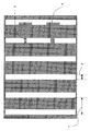
誘電体上に、1層目の感光性ペーストを塗布した。感光性ペーストは、ガラス粉末と感光性成分を含む有機成分から構成され、ガラス粉末には、酸化リチウム10重量%、酸化珪素25重量%、酸化硼素30重量%、酸化亜鉛15重量%、酸化アルミニウム5重量%、および酸化カルシウム15重量%からなる組成のガラスを粉砕した、平均粒子径2μmのガラス粉末を用いた。感光性成分を含む有機成分には、カルボキシル基を含有するアクリルポリマー30重量%、トリメチロールプロパントリアクリレート30重量%、光重合開始剤である“イルガキュア(登録商標)651”(チバガイギー社製)10重量%、およびジエチレングリコールモノブチルエーテルアセテート30重量%からなるものを用いた。感光性ペーストは、これらのガラス粉末と感光性成分を含む有機成分をそれぞれ70:30の重量比率で混合した後に、ロールミルで混練して作製した。次に、この感光性ペーストをダイコーターを用いて乾燥後厚さ180μm、塗布幅520mmになるように塗布した。乾燥は、IR乾燥炉(日本ガイシ社製)で行った。乾燥後、ピッチ1が250μm、線幅2が20μmのストライプパターンを有するフォトマスクA(図1)を用いて、アドレス電極と平行方向に露光した。このとき、フォトマスクAの一部には疑似欠陥部3、4を形成した。露光後、上記感光性ペーストをさらに塗布、乾燥し、乾燥後厚さ70μm、塗布膜幅522mmの感光性塗布膜を得た。
A first layer of photosensitive paste was applied on the dielectric. The photosensitive paste is composed of glass powder and an organic component containing a photosensitive component. The glass powder includes 10% by weight of lithium oxide, 25% by weight of silicon oxide, 30% by weight of boron oxide, 15% by weight of zinc oxide, and aluminum oxide. A glass powder having an average particle diameter of 2 μm, obtained by pulverizing a glass composed of 5% by weight and 15% by weight of calcium oxide, was used. The organic component including the photosensitive component includes 30% by weight of an acrylic polymer containing a carboxyl group, 30% by weight of trimethylolpropane triacrylate, “Irgacure (registered trademark) 651” (manufactured by Ciba Geigy) 10 A composition consisting of 30% by weight and 30% by weight of diethylene glycol monobutyl ether acetate was used. The photosensitive paste was prepared by mixing the glass powder and the organic component containing the photosensitive component in a weight ratio of 70:30, and then kneading them with a roll mill. Next, this photosensitive paste was applied by using a die coater so as to have a thickness of 180 μm and a coating width of 520 mm after drying. Drying was performed in an IR drying furnace (manufactured by NGK). After drying, exposure was performed in a direction parallel to the address electrodes using a photomask A (FIG. 1) having a stripe pattern with a pitch 1 of 250 μm and a line width 2 of 20 μm. At this time,
次に、ピッチ250μm、線幅40μmのストライプパターンを有するフォトマスクB(図2)を用いて、アドレス電極と平行方向に露光した。露光後、0.5重量%のエタノールアミン水溶液中で現像し、さらに、560℃の温度で15分間焼成することにより隔壁を形成した。得られた隔壁には、マスク起因の欠陥や隔壁端部の跳ね上がりは観察されなかった。 Next, using a photomask B (FIG. 2) having a stripe pattern with a pitch of 250 μm and a line width of 40 μm, exposure was performed in a direction parallel to the address electrodes. After the exposure, development was carried out in a 0.5% by weight ethanolamine aqueous solution, followed by baking at a temperature of 560 ° C. for 15 minutes to form partition walls. In the obtained partition wall, no defect due to the mask and no jumping up of the end of the partition wall were observed.
次に、隣り合う隔壁間に蛍光体を塗布した。蛍光体の塗布は、256カ所の穴(口径:130μm)が形成されたノズル先端から蛍光体ペーストを吐出するディスペンサー法により形成した。蛍光体は隔壁側面に焼成後厚さ25μm、誘電体上に焼成後厚さ25μmになるように塗布した後に、500℃で10分間の焼成を行った。かくしてPDP用部材として、背面板を作製した。 Next, a phosphor was applied between adjacent barrier ribs. The phosphor was applied by a dispenser method in which the phosphor paste was discharged from the tip of a nozzle in which 256 holes (caliber: 130 μm) were formed. The phosphor was fired at 500 ° C. for 10 minutes after being applied on the side walls of the barrier ribs so that the thickness was 25 μm after firing and on the dielectric so that the thickness was 25 μm after firing. Thus, a back plate was produced as a member for PDP.
さらに、作製した前面基板と背面基板を封着ガラスを用いて封着して、Xe5%含有のNeガスを内部ガス圧66500Paになるように封入した。さらに、駆動回路を実装してPDPを作製した。PDPのスキャン電極に電圧を印加して発光させた。その輝度計を用いて輝度を測定したところ、220cd/m2であり、表示特性は良好であった。また、面内で表示むらは見られなかった。
Further, the produced front substrate and back substrate were sealed using sealing glass, and Ne
実施例2
隔壁パターンの形成において、1層目の感光性塗布膜の露光時に図3に示すフォトマスクCを用いた他は、実施例1と同様に行った。フォトマスクCは、アドレス電極と平行方向にピッチ250μm、線幅20μm、アドレス方向と垂直方向に線幅60μmのパターンが形成されたものであり、パターンの一部に疑似欠陥部5、6を形成した。パターン形成後は、壁状の突起部が隔壁と交差する方向に隔壁より低く形成された形となる。得られた隔壁および壁状の突起部のパターンには、欠けや隔壁端部の跳ね上がりは見られなかった。さらに、得られたPDPのスキャン電極に電圧を印加して発光させた。その輝度計を用いて輝度を測定したところ、260cd/m2であり、高い輝度の表示特性を得ることができた。また、面内で表示むらは見られなかった。
Example 2
The partition pattern was formed in the same manner as Example 1 except that the photomask C shown in FIG. The photomask C has a pattern with a pitch of 250 μm in the direction parallel to the address electrodes, a line width of 20 μm, and a line width of 60 μm in the direction perpendicular to the address direction.
比較例1
隔壁パターン形成において、2層目の塗布幅を1層目と同じ幅(520mm)とし、2層目の露光時にフォトマスクを1層目と同じようにフォトマスクAを用いた他は、実施例1と同様に行った。得られた隔壁パターンには、マスク欠陥に起因する欠けや端部の跳ね上がりが観察させた。さらに、得られたPDPのスキャン電極に電圧を印加して発光させたところ、隔壁パターンの欠け部や端部の跳ね上がり部に表示むらが現れ、表示特性は不良であった。
Comparative Example 1
In the partition wall pattern formation, the coating width of the second layer was set to the same width (520 mm) as that of the first layer, and the photomask A was used in the same manner as the first layer in the exposure of the second layer. 1 was performed. In the obtained partition wall pattern, chipping and edge jumping due to mask defects were observed. Furthermore, when a voltage was applied to the scan electrode of the obtained PDP to emit light, display unevenness appeared at the notched portion of the partition wall pattern and the jumped-up portion of the end portion, and the display characteristics were poor.
本発明のプラズマディスプレイ用部材は、壁掛けテレビや大型モニターに用いられ、特に、プラズマディスプレイパネルの輝度を向上し、パネルの表示品位を高めたプラズマディスプレイプラズマディスプレイの製造に好適である。 The member for a plasma display of the present invention is used for a wall-mounted television or a large monitor, and is particularly suitable for manufacturing a plasma display plasma display in which the brightness of the plasma display panel is improved and the display quality of the panel is improved.
1 ピッチ
2 線幅
3 疑似欠陥
4 疑似欠陥
5 疑似欠陥
6 疑似欠陥
1 Pitch 2
Claims (5)
(A)前記隔壁の一部となる1層目のパターン形成用感光性塗布膜を形成する工程、
(B)前記1層目のパターン形成用感光性塗布膜を第1のフォトマスクを介して露光する工程、
(C)前記隔壁の一部となる2層目のパターン形成用感光性塗布膜を前記1層目のパターン形成用感光性塗布膜幅よりも広く形成する工程、
(D)前記2層目のパターン形成用感光性塗布膜を第2のフォトマスクを介して露光する工程、
(E)現像する工程、
(F)焼成する工程。 A method of manufacturing a plasma display panel comprising a step of forming the partition wall, the production of plasma display panel to form a pattern of the partition wall is equal to or going through successively the steps below (A) ~ (F) Method.
(A) a step of forming a first-layer pattern-forming photosensitive coating film that becomes a part of the partition ;
(B) exposing the first layer pattern forming photosensitive coating film through a first photomask;
(C) forming a second layer pattern forming photosensitive coating film, which is a part of the partition wall, wider than the first layer pattern forming photosensitive coating film;
(D) exposing the second layer pattern-forming photosensitive coating film through a second photomask;
(E) developing step,
(F) A step of firing.
Priority Applications (1)
| Application Number | Priority Date | Filing Date | Title |
|---|---|---|---|
| JP2003383610A JP4540968B2 (en) | 2003-11-13 | 2003-11-13 | Plasma display panel manufacturing method and plasma display |
Applications Claiming Priority (1)
| Application Number | Priority Date | Filing Date | Title |
|---|---|---|---|
| JP2003383610A JP4540968B2 (en) | 2003-11-13 | 2003-11-13 | Plasma display panel manufacturing method and plasma display |
Publications (2)
| Publication Number | Publication Date |
|---|---|
| JP2005149832A JP2005149832A (en) | 2005-06-09 |
| JP4540968B2 true JP4540968B2 (en) | 2010-09-08 |
Family
ID=34692281
Family Applications (1)
| Application Number | Title | Priority Date | Filing Date |
|---|---|---|---|
| JP2003383610A Expired - Fee Related JP4540968B2 (en) | 2003-11-13 | 2003-11-13 | Plasma display panel manufacturing method and plasma display |
Country Status (1)
| Country | Link |
|---|---|
| JP (1) | JP4540968B2 (en) |
Families Citing this family (1)
| Publication number | Priority date | Publication date | Assignee | Title |
|---|---|---|---|---|
| JP4670774B2 (en) * | 2006-08-31 | 2011-04-13 | パナソニック株式会社 | Manufacturing method of back plate for plasma display |
Citations (21)
| Publication number | Priority date | Publication date | Assignee | Title |
|---|---|---|---|---|
| JPS59232418A (en) * | 1983-06-15 | 1984-12-27 | Sumitomo Electric Ind Ltd | Formation of fine pattern |
| JPH0577287B2 (en) * | 1987-04-15 | 1993-10-26 | Rohm Kk | |
| JPH05335196A (en) * | 1992-05-27 | 1993-12-17 | Hitachi Ltd | Forming method of photomask pattern, exposing method of negative photosensitive resin, and substrate |
| JPH06333804A (en) * | 1993-05-20 | 1994-12-02 | Fujitsu Ltd | X-ray exposure method and manufacture of x-ray mask |
| JPH08335439A (en) * | 1995-06-07 | 1996-12-17 | Dainippon Printing Co Ltd | Cathode of dc type plasma display panel and its formation |
| JPH10241580A (en) * | 1997-02-27 | 1998-09-11 | Toppan Printing Co Ltd | Plasma display and its manufacture |
| JPH1190827A (en) * | 1997-09-16 | 1999-04-06 | Fujitsu Ltd | Sand-blasting method |
| JP2000156151A (en) * | 1998-11-17 | 2000-06-06 | Nec Corp | Plasma display panel and manufacture thereof |
| JP2000181074A (en) * | 1998-12-15 | 2000-06-30 | Sharp Corp | Method for exposing photosensitive layer |
| JP2001101970A (en) * | 1999-09-30 | 2001-04-13 | Toppan Printing Co Ltd | Dielectric for plasma display panel and method for forming barrier rib |
| JP2001110305A (en) * | 1999-10-06 | 2001-04-20 | Dainippon Printing Co Ltd | Barrier rib forming method for plasma display panel |
| JP2001176401A (en) * | 1999-12-17 | 2001-06-29 | Toray Ind Inc | Member for plasma display, manufacturing method therefor and plasma display |
| JP2001236892A (en) * | 1999-10-19 | 2001-08-31 | Matsushita Electric Ind Co Ltd | Electrode, its manufacturing method, plasma display and its manufacturing method |
| JP2001307623A (en) * | 2000-04-24 | 2001-11-02 | Mitsubishi Electric Corp | Manufacturing method of substrate for ac type plasma display panel, sunstrate for ac type plasma display panel, ac type plasma display panel and ac type plasma display device |
| JP2002015662A (en) * | 2000-06-28 | 2002-01-18 | Toray Ind Inc | Manufacturing method of component for plasma display, and plasma display |
| JP2002216618A (en) * | 2001-01-23 | 2002-08-02 | Matsushita Electric Ind Co Ltd | Manufacturing method for plasma display device |
| JP2003162065A (en) * | 2001-11-26 | 2003-06-06 | Mitsubishi Electric Corp | Exposure system, mask for exposure, exposure method, display, and electronic parts |
| JP2004265867A (en) * | 2003-02-14 | 2004-09-24 | Toray Ind Inc | Method of manufacturing display member, display member, and display using it |
| JP2004265634A (en) * | 2003-02-21 | 2004-09-24 | Matsushita Electric Ind Co Ltd | Manufacturing method of plasma display panel |
| JP2004273447A (en) * | 2003-02-17 | 2004-09-30 | Toray Ind Inc | Method for manufacturing display member, display member using the same and display |
| JP2004342348A (en) * | 2003-05-13 | 2004-12-02 | Matsushita Electric Ind Co Ltd | Manufacturing method of plasma display panel |
-
2003
- 2003-11-13 JP JP2003383610A patent/JP4540968B2/en not_active Expired - Fee Related
Patent Citations (21)
| Publication number | Priority date | Publication date | Assignee | Title |
|---|---|---|---|---|
| JPS59232418A (en) * | 1983-06-15 | 1984-12-27 | Sumitomo Electric Ind Ltd | Formation of fine pattern |
| JPH0577287B2 (en) * | 1987-04-15 | 1993-10-26 | Rohm Kk | |
| JPH05335196A (en) * | 1992-05-27 | 1993-12-17 | Hitachi Ltd | Forming method of photomask pattern, exposing method of negative photosensitive resin, and substrate |
| JPH06333804A (en) * | 1993-05-20 | 1994-12-02 | Fujitsu Ltd | X-ray exposure method and manufacture of x-ray mask |
| JPH08335439A (en) * | 1995-06-07 | 1996-12-17 | Dainippon Printing Co Ltd | Cathode of dc type plasma display panel and its formation |
| JPH10241580A (en) * | 1997-02-27 | 1998-09-11 | Toppan Printing Co Ltd | Plasma display and its manufacture |
| JPH1190827A (en) * | 1997-09-16 | 1999-04-06 | Fujitsu Ltd | Sand-blasting method |
| JP2000156151A (en) * | 1998-11-17 | 2000-06-06 | Nec Corp | Plasma display panel and manufacture thereof |
| JP2000181074A (en) * | 1998-12-15 | 2000-06-30 | Sharp Corp | Method for exposing photosensitive layer |
| JP2001101970A (en) * | 1999-09-30 | 2001-04-13 | Toppan Printing Co Ltd | Dielectric for plasma display panel and method for forming barrier rib |
| JP2001110305A (en) * | 1999-10-06 | 2001-04-20 | Dainippon Printing Co Ltd | Barrier rib forming method for plasma display panel |
| JP2001236892A (en) * | 1999-10-19 | 2001-08-31 | Matsushita Electric Ind Co Ltd | Electrode, its manufacturing method, plasma display and its manufacturing method |
| JP2001176401A (en) * | 1999-12-17 | 2001-06-29 | Toray Ind Inc | Member for plasma display, manufacturing method therefor and plasma display |
| JP2001307623A (en) * | 2000-04-24 | 2001-11-02 | Mitsubishi Electric Corp | Manufacturing method of substrate for ac type plasma display panel, sunstrate for ac type plasma display panel, ac type plasma display panel and ac type plasma display device |
| JP2002015662A (en) * | 2000-06-28 | 2002-01-18 | Toray Ind Inc | Manufacturing method of component for plasma display, and plasma display |
| JP2002216618A (en) * | 2001-01-23 | 2002-08-02 | Matsushita Electric Ind Co Ltd | Manufacturing method for plasma display device |
| JP2003162065A (en) * | 2001-11-26 | 2003-06-06 | Mitsubishi Electric Corp | Exposure system, mask for exposure, exposure method, display, and electronic parts |
| JP2004265867A (en) * | 2003-02-14 | 2004-09-24 | Toray Ind Inc | Method of manufacturing display member, display member, and display using it |
| JP2004273447A (en) * | 2003-02-17 | 2004-09-30 | Toray Ind Inc | Method for manufacturing display member, display member using the same and display |
| JP2004265634A (en) * | 2003-02-21 | 2004-09-24 | Matsushita Electric Ind Co Ltd | Manufacturing method of plasma display panel |
| JP2004342348A (en) * | 2003-05-13 | 2004-12-02 | Matsushita Electric Ind Co Ltd | Manufacturing method of plasma display panel |
Also Published As
| Publication number | Publication date |
|---|---|
| JP2005149832A (en) | 2005-06-09 |
Similar Documents
| Publication | Publication Date | Title |
|---|---|---|
| JP4957546B2 (en) | Plasma display member and manufacturing method thereof | |
| JP4333741B2 (en) | Display member exposure method and plasma display member manufacturing method | |
| JP2006310280A (en) | Back plate for plasma display and plasma display panel | |
| JP4281689B2 (en) | Plasma display panel member and plasma display panel using the same | |
| JP4161479B2 (en) | Plasma display member and plasma display manufacturing method | |
| JP2006294501A (en) | Member for plasma display | |
| JP4540968B2 (en) | Plasma display panel manufacturing method and plasma display | |
| JP2005025950A (en) | Plasma display member | |
| JP5024368B2 (en) | Plasma display member and method for manufacturing plasma display member | |
| JP4320886B2 (en) | Plasma display member, method of manufacturing the same, and plasma display | |
| JP4554772B2 (en) | Method for manufacturing plasma display member | |
| JP4531168B2 (en) | Manufacturing method of plasma display | |
| JP4479032B2 (en) | Plasma display member and plasma display | |
| JP2001023515A (en) | Manufacture of plasma display material and plasma display | |
| JP2005025951A (en) | Plasma display member and its manufacturing method | |
| JP5293485B2 (en) | Method for manufacturing plasma display member | |
| JP4670774B2 (en) | Manufacturing method of back plate for plasma display | |
| JP4867326B2 (en) | Plasma display panel | |
| JP5256674B2 (en) | Plasma display panel | |
| JP5404499B2 (en) | Back plate for plasma display | |
| JP5025907B2 (en) | Method for manufacturing plasma display panel | |
| JP2008181872A (en) | Member for plasma display | |
| JP2005025949A (en) | Plasma display member and its manufacturing method | |
| JP2007200878A (en) | Method of manufacturing member for plasma display panel | |
| JP2009087625A (en) | Plasma display panel |
Legal Events
| Date | Code | Title | Description |
|---|---|---|---|
| A621 | Written request for application examination |
Free format text: JAPANESE INTERMEDIATE CODE: A621 Effective date: 20061113 |
|
| A131 | Notification of reasons for refusal |
Free format text: JAPANESE INTERMEDIATE CODE: A131 Effective date: 20091013 |
|
| A521 | Written amendment |
Free format text: JAPANESE INTERMEDIATE CODE: A523 Effective date: 20091209 |
|
| A131 | Notification of reasons for refusal |
Free format text: JAPANESE INTERMEDIATE CODE: A131 Effective date: 20100112 |
|
| A521 | Written amendment |
Free format text: JAPANESE INTERMEDIATE CODE: A523 Effective date: 20100309 |
|
| A711 | Notification of change in applicant |
Free format text: JAPANESE INTERMEDIATE CODE: A711 Effective date: 20100319 |
|
| A131 | Notification of reasons for refusal |
Free format text: JAPANESE INTERMEDIATE CODE: A131 Effective date: 20100420 |
|
| A521 | Written amendment |
Free format text: JAPANESE INTERMEDIATE CODE: A523 Effective date: 20100526 |
|
| TRDD | Decision of grant or rejection written | ||
| A01 | Written decision to grant a patent or to grant a registration (utility model) |
Free format text: JAPANESE INTERMEDIATE CODE: A01 Effective date: 20100615 |
|
| A01 | Written decision to grant a patent or to grant a registration (utility model) |
Free format text: JAPANESE INTERMEDIATE CODE: A01 |
|
| A61 | First payment of annual fees (during grant procedure) |
Free format text: JAPANESE INTERMEDIATE CODE: A61 Effective date: 20100623 |
|
| R150 | Certificate of patent or registration of utility model |
Free format text: JAPANESE INTERMEDIATE CODE: R150 |
|
| FPAY | Renewal fee payment (event date is renewal date of database) |
Free format text: PAYMENT UNTIL: 20130702 Year of fee payment: 3 |
|
| LAPS | Cancellation because of no payment of annual fees |