JP4533058B2 - 照明装置用反射板 - Google Patents
照明装置用反射板 Download PDFInfo
- Publication number
- JP4533058B2 JP4533058B2 JP2004264338A JP2004264338A JP4533058B2 JP 4533058 B2 JP4533058 B2 JP 4533058B2 JP 2004264338 A JP2004264338 A JP 2004264338A JP 2004264338 A JP2004264338 A JP 2004264338A JP 4533058 B2 JP4533058 B2 JP 4533058B2
- Authority
- JP
- Japan
- Prior art keywords
- opening
- reflector
- hole
- substrate
- plating film
- Prior art date
- Legal status (The legal status is an assumption and is not a legal conclusion. Google has not performed a legal analysis and makes no representation as to the accuracy of the status listed.)
- Expired - Fee Related
Links
Images


Classifications
-
- H—ELECTRICITY
- H01—ELECTRIC ELEMENTS
- H01L—SEMICONDUCTOR DEVICES NOT COVERED BY CLASS H10
- H01L2224/00—Indexing scheme for arrangements for connecting or disconnecting semiconductor or solid-state bodies and methods related thereto as covered by H01L24/00
- H01L2224/01—Means for bonding being attached to, or being formed on, the surface to be connected, e.g. chip-to-package, die-attach, "first-level" interconnects; Manufacturing methods related thereto
- H01L2224/10—Bump connectors; Manufacturing methods related thereto
- H01L2224/15—Structure, shape, material or disposition of the bump connectors after the connecting process
- H01L2224/16—Structure, shape, material or disposition of the bump connectors after the connecting process of an individual bump connector
Description
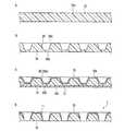
まず、本発明の第1実施形態に係る反射板について適宜図面を参照して説明する。参照する図1は、第1実施形態に係る反射板の断面図である。
次に、本発明の第2実施形態に係る照明装置について適宜図面を参照して説明する。参照する図3は、第2実施形態に係る照明装置の断面図である。なお、図1と同一の構成要素には同一の符号を付し、その説明は省略する。
1a,1b,10a,10b 主面
2 照明装置
10 電気絶縁基材
11,41 貫通孔
12 第1開口
13 第2開口
13a エッジ
14,20c 内壁面
14a 第1傾斜面
14b 第2傾斜面
15 めっき膜
15a 端部
20 有底穴
20a 開口
20b 底部
21 マスキングシート
30 ベース層
31 電気絶縁層
32 配線パターン
33 基板
34 バンプ
35 LED(発光素子)
36 接着層
40 接着シート
50 積層体
131a 稜線
Claims (3)
- 樹脂材料を含む電気絶縁基材と、前記電気絶縁基材に形成され、発光素子を収容するための貫通孔とを有する照明装置用反射板であって、
前記貫通孔は、第1開口と、前記第1開口より一回り小さい第2開口とを有し、
前記貫通孔の内壁面は、前記第1開口から前記第2開口に向けて狭まるすり鉢状に形成され、かつ一部がめっき膜で覆われており、
前記照明装置用反射板の前記第2開口側の主面及び前記第2開口のエッジは、前記電気絶縁基材の構成材料が露出しており、且つ前記貫通孔の内壁面を覆う前記めっき膜のうち前記第2開口のエッジに最も近い端部と、前記第2開口のエッジの稜線との距離は、100μm以上であり、前記貫通孔の内壁面は、前記第1開口側に位置し、前記めっき膜で覆われている第1傾斜面と、前記第2開口側に位置し、前記電気絶縁基材の構成材料が露出している第2傾斜面とからなり、
前記照明装置用反射板の前記第2開口側の主面に対する前記第2傾斜面の傾斜角度は、前記主面に対する前記第1傾斜面の傾斜角度よりも大きく、且つ前記第2傾斜面の傾斜角度が40°から80°であることを特徴とする照明装置用反射板。 - すり鉢状に形成された貫通孔の内壁面における前記めっき膜の厚さが第1開口部側から、第2開口部側に向けて薄くなり、且つ第2開口部のエッジにおいては、めっき膜を有しない請求項1に記載の照明装置用反射板。
- 主面及びすり鉢状に形成された有底穴における内壁面を覆っためっき膜を、当該有底穴の径以上の直径を有するパンチを用いたプレス加工を当該すり鉢状の有底穴部に施すことによって、反射板に貫通孔を形成させて第2開口部を得た請求項2に記載の照明装置用反射板。
Priority Applications (1)
| Application Number | Priority Date | Filing Date | Title |
|---|---|---|---|
| JP2004264338A JP4533058B2 (ja) | 2004-09-10 | 2004-09-10 | 照明装置用反射板 |
Applications Claiming Priority (1)
| Application Number | Priority Date | Filing Date | Title |
|---|---|---|---|
| JP2004264338A JP4533058B2 (ja) | 2004-09-10 | 2004-09-10 | 照明装置用反射板 |
Publications (3)
| Publication Number | Publication Date |
|---|---|
| JP2006080003A JP2006080003A (ja) | 2006-03-23 |
| JP2006080003A5 JP2006080003A5 (ja) | 2007-08-16 |
| JP4533058B2 true JP4533058B2 (ja) | 2010-08-25 |
Family
ID=36159270
Family Applications (1)
| Application Number | Title | Priority Date | Filing Date |
|---|---|---|---|
| JP2004264338A Expired - Fee Related JP4533058B2 (ja) | 2004-09-10 | 2004-09-10 | 照明装置用反射板 |
Country Status (1)
| Country | Link |
|---|---|
| JP (1) | JP4533058B2 (ja) |
Families Citing this family (7)
| Publication number | Priority date | Publication date | Assignee | Title |
|---|---|---|---|---|
| JP4863193B2 (ja) * | 2005-08-31 | 2012-01-25 | スタンレー電気株式会社 | 半導体発光装置 |
| US20090032829A1 (en) * | 2007-07-30 | 2009-02-05 | Tong Fatt Chew | LED Light Source with Increased Thermal Conductivity |
| JP5064254B2 (ja) * | 2008-01-30 | 2012-10-31 | 日東電工株式会社 | 光半導体素子封止用樹脂シートおよび光半導体装置 |
| JP5077679B2 (ja) * | 2008-02-29 | 2012-11-21 | 日立化成工業株式会社 | 貼り合わせ基板の製造方法 |
| JP2010238596A (ja) * | 2009-03-31 | 2010-10-21 | Showa Denko Kk | 照明装置 |
| JP5394899B2 (ja) * | 2009-11-19 | 2014-01-22 | パナソニック株式会社 | 反射板 |
| JP2013030599A (ja) * | 2011-07-28 | 2013-02-07 | Sumitomo Bakelite Co Ltd | 発光デバイスおよび照明器具 |
Citations (4)
| Publication number | Priority date | Publication date | Assignee | Title |
|---|---|---|---|---|
| JPH07202271A (ja) * | 1993-12-28 | 1995-08-04 | Matsushita Electric Works Ltd | 発光ダイオード及びその製造方法 |
| JP2002344108A (ja) * | 2001-05-17 | 2002-11-29 | Hitachi Aic Inc | プリント配線板およびその製造方法およびそれを使用した実装体 |
| JP2003218401A (ja) * | 2002-01-18 | 2003-07-31 | Matsushita Electric Ind Co Ltd | 半導体発光装置およびその製造方法 |
| JP2004241509A (ja) * | 2003-02-04 | 2004-08-26 | Matsushita Electric Ind Co Ltd | Led光源、led照明装置、およびled表示装置 |
-
2004
- 2004-09-10 JP JP2004264338A patent/JP4533058B2/ja not_active Expired - Fee Related
Patent Citations (4)
| Publication number | Priority date | Publication date | Assignee | Title |
|---|---|---|---|---|
| JPH07202271A (ja) * | 1993-12-28 | 1995-08-04 | Matsushita Electric Works Ltd | 発光ダイオード及びその製造方法 |
| JP2002344108A (ja) * | 2001-05-17 | 2002-11-29 | Hitachi Aic Inc | プリント配線板およびその製造方法およびそれを使用した実装体 |
| JP2003218401A (ja) * | 2002-01-18 | 2003-07-31 | Matsushita Electric Ind Co Ltd | 半導体発光装置およびその製造方法 |
| JP2004241509A (ja) * | 2003-02-04 | 2004-08-26 | Matsushita Electric Ind Co Ltd | Led光源、led照明装置、およびled表示装置 |
Also Published As
| Publication number | Publication date |
|---|---|
| JP2006080003A (ja) | 2006-03-23 |
Similar Documents
| Publication | Publication Date | Title |
|---|---|---|
| JP4085917B2 (ja) | 高熱伝導性発光素子用回路部品及び高放熱モジュール | |
| JP4062358B2 (ja) | Led装置 | |
| JP4754850B2 (ja) | Led実装用モジュールの製造方法及びledモジュールの製造方法 | |
| US9698563B2 (en) | Flexible LED device and method of making | |
| JP4735941B2 (ja) | 発光素子用の配線基板 | |
| US20140321126A1 (en) | Flexible light emitting semiconductor device having a three dimensional structure | |
| US20100149823A1 (en) | Lamp unit, circuit board, and method of manufaturing circuit board | |
| JP5940799B2 (ja) | 電子部品搭載用パッケージ及び電子部品パッケージ並びにそれらの製造方法 | |
| JP2008258617A (ja) | メタルpcbを有するledパッケージ | |
| US20060018120A1 (en) | Illuminator and production method | |
| JP2007234846A (ja) | 発光素子用セラミックパッケージ | |
| JP4127220B2 (ja) | Led実装用プリント基板及びその製造方法 | |
| JP2006287126A (ja) | Ledランプ、およびそのユニット板の製造方法 | |
| US9756730B2 (en) | Chip-integrated through-plating of multi-layer substrates | |
| JP4533058B2 (ja) | 照明装置用反射板 | |
| US9685391B2 (en) | Wiring board and semiconductor package | |
| JP2005310935A (ja) | 発光素子収納用パッケージ | |
| TW201037803A (en) | Multi-layer packaging substrate, method for making the packaging substrate, and package structure of light-emitting semiconductor | |
| JP5183965B2 (ja) | 照明装置の製造方法 | |
| JP2006066531A (ja) | 照明装置及びその製造方法 | |
| KR20110045273A (ko) | 패키지용 인쇄회로기판 및 그 제조방법 | |
| KR101163893B1 (ko) | 방열회로기판 및 그의 제조 방법 | |
| JP5130015B2 (ja) | 発光ダイオード用パッケージ及びその製造方法並びに発光ダイオード用パッケージを用いた発光ダイオード | |
| JP2007073718A (ja) | 発光素子収納用パッケージ | |
| JP2006261286A (ja) | 発光素子収納用パッケージ及びその製造方法 |
Legal Events
| Date | Code | Title | Description |
|---|---|---|---|
| A521 | Written amendment |
Free format text: JAPANESE INTERMEDIATE CODE: A523 Effective date: 20070629 |
|
| A621 | Written request for application examination |
Free format text: JAPANESE INTERMEDIATE CODE: A621 Effective date: 20070629 |
|
| A977 | Report on retrieval |
Free format text: JAPANESE INTERMEDIATE CODE: A971007 Effective date: 20090716 |
|
| A131 | Notification of reasons for refusal |
Free format text: JAPANESE INTERMEDIATE CODE: A131 Effective date: 20091105 |
|
| A521 | Written amendment |
Free format text: JAPANESE INTERMEDIATE CODE: A523 Effective date: 20091225 |
|
| TRDD | Decision of grant or rejection written | ||
| A01 | Written decision to grant a patent or to grant a registration (utility model) |
Free format text: JAPANESE INTERMEDIATE CODE: A01 Effective date: 20100608 |
|
| A01 | Written decision to grant a patent or to grant a registration (utility model) |
Free format text: JAPANESE INTERMEDIATE CODE: A01 |
|
| A61 | First payment of annual fees (during grant procedure) |
Free format text: JAPANESE INTERMEDIATE CODE: A61 Effective date: 20100611 |
|
| R150 | Certificate of patent or registration of utility model |
Free format text: JAPANESE INTERMEDIATE CODE: R150 |
|
| FPAY | Renewal fee payment (event date is renewal date of database) |
Free format text: PAYMENT UNTIL: 20130618 Year of fee payment: 3 |
|
| LAPS | Cancellation because of no payment of annual fees |