JP4533058B2 - Reflector for lighting device - Google Patents
Reflector for lighting device Download PDFInfo
- Publication number
- JP4533058B2 JP4533058B2 JP2004264338A JP2004264338A JP4533058B2 JP 4533058 B2 JP4533058 B2 JP 4533058B2 JP 2004264338 A JP2004264338 A JP 2004264338A JP 2004264338 A JP2004264338 A JP 2004264338A JP 4533058 B2 JP4533058 B2 JP 4533058B2
- Authority
- JP
- Japan
- Prior art keywords
- opening
- reflector
- hole
- substrate
- plating film
- Prior art date
- Legal status (The legal status is an assumption and is not a legal conclusion. Google has not performed a legal analysis and makes no representation as to the accuracy of the status listed.)
- Expired - Fee Related
Links
Images


Classifications
-
- H—ELECTRICITY
- H01—ELECTRIC ELEMENTS
- H01L—SEMICONDUCTOR DEVICES NOT COVERED BY CLASS H10
- H01L2224/00—Indexing scheme for arrangements for connecting or disconnecting semiconductor or solid-state bodies and methods related thereto as covered by H01L24/00
- H01L2224/01—Means for bonding being attached to, or being formed on, the surface to be connected, e.g. chip-to-package, die-attach, "first-level" interconnects; Manufacturing methods related thereto
- H01L2224/10—Bump connectors; Manufacturing methods related thereto
- H01L2224/15—Structure, shape, material or disposition of the bump connectors after the connecting process
- H01L2224/16—Structure, shape, material or disposition of the bump connectors after the connecting process of an individual bump connector
Description
本発明は、照明装置用反射板とその製造方法、及びこれを用いた照明装置とその製造方法に関する。 The present invention relates to a reflector for an illuminating device and a manufacturing method thereof, and an illuminating device using the same and a manufacturing method thereof.
照明器具や看板の光源として、従来から白熱電球、蛍光ランプ、高圧放電ランプ等が使用されている。これらの光源にかわる新しい照明光源として、発光ダイオード(LED)やエレクトロルミネッセンス(EL)素子等の発光素子の研究が進められている。また、これらの発光素子を用いた照明装置についても研究が進められており、中でもLEDを用いた照明装置(以下、「LED照明装置」ともいう)は、従来の照明装置と比べて寿命が長いという優れた利点があるため、様々なLED照明装置が提案されている(例えば特許文献1参照)。 Conventionally, incandescent bulbs, fluorescent lamps, high-pressure discharge lamps, and the like have been used as light sources for lighting fixtures and signboards. As new illumination light sources that replace these light sources, research on light-emitting elements such as light-emitting diodes (LEDs) and electroluminescence (EL) elements is underway. In addition, research is also being conducted on lighting devices using these light-emitting elements. Among them, lighting devices using LEDs (hereinafter also referred to as “LED lighting devices”) have a longer lifetime than conventional lighting devices. Therefore, various LED lighting devices have been proposed (see, for example, Patent Document 1).
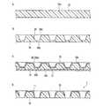
図7は、特許文献1に提案されたLED照明装置の構成を示し、このうち図7AはLED照明装置の全体斜視図を示し、図7Bは図7AのI−I線断面図を示す。 7 shows the configuration of the LED lighting device proposed in Patent Document 1, in which FIG. 7A shows an overall perspective view of the LED lighting device, and FIG. 7B shows a cross-sectional view taken along the line I-I in FIG. 7A.
図7Aに示すように、特許文献1に提案されたLED照明装置100は、基板101と、基板101に実装された複数のLED102と、複数のLED102のそれぞれを収容する複数の貫通孔103を有する反射板104とを含む。また、基板101と反射板104とは、接着層105を介して貼り合わされている。
As illustrated in FIG. 7A, the
図7Bに示すように、基板101は、ベース層110と、ベース層110上に積層された樹脂材料を含む電気絶縁層111と、電気絶縁層111上に形成された配線パターン112とを含む。LED102は、配線パターン112上に、バンプ113を介して実装され、例えば図示しない封止樹脂で封止されている。また、貫通孔103の内壁面103aは、基板101側に向かって狭まるすり鉢状に形成されている。
As illustrated in FIG. 7B, the
このように構成されたLED照明装置100において、LED102から発生した光は、例えば外部へ直接出射し(図7Bの矢印II)、あるいは貫通孔103の内壁面103aで反射されて外部へ出射することにより(図7Bの矢印III)、照明光として利用される。
In the
上述したLED照明装置100を含む従来のLED照明装置では、反射板として、通常、アルミニウム板等の金属製の反射板が使用されている。しかしながら、金属製の反射板を用いると、以下に示すような問題点が生じる。即ち、金属製の反射板が貼り合わされる基板の電気絶縁層は、例えばエポキシ樹脂等の樹脂材料を主成分とするため、反射板の線膨張係数と電気絶縁層の線膨張係数との差が大き過ぎて、反射板と基板との界面にクラックが発生し易くなる。その結果、反射板と基板との密着性が悪化し、その界面で剥離が生ずるおそれがある。
In the conventional LED illumination device including the
他方、反射板の構成材料としてプラスチック材を用いたLED照明装置が、特許文献2に提案されている。特許文献2のLED照明装置によれば、反射板の線膨張係数と電気絶縁層の線膨張係数との差を小さくすることができるため、反射板と基板との密着性が改善される。更に、特許文献2には、前記反射板の反射面が無電解Niめっき膜で覆われたLED照明装置についても提案されている。この構成によれば、反射板を構成するプラスチック材が、LEDの照射光により劣化することを防止できる。よって、例えば、反射板の変色に起因する照明光の色ズレ等を防止できる。
しかし、反射板の反射面を無電解Niめっき膜等のめっき膜で覆うと、このめっき膜とLEDが実装された配線パターンとが短絡し、その結果、例えば複数のLED間が、反射板(即ち、反射板に設けられためっき膜)を通じて短絡するおそれがある。 However, when the reflecting surface of the reflecting plate is covered with a plating film such as an electroless Ni plating film, the plating film and the wiring pattern on which the LED is mounted are short-circuited. That is, there is a risk of short circuit through the plating film provided on the reflector.
本発明は、前記従来の課題を解決するもので、基板との密着性を向上させた上で、発光素子の照射光による劣化、及び基板に形成された配線パターンとの短絡を防止できる照明装置用反射板とその製造方法、及びこれを用いた照明装置とその製造方法を提供する。 The present invention solves the above-mentioned conventional problems, and can improve the adhesion to the substrate, and can prevent deterioration of the light emitting element due to irradiation light and short circuit with the wiring pattern formed on the substrate. Provided are a reflector for light and a method for manufacturing the same, and an illumination device using the same and a method for manufacturing the same.
本発明の照明装置用反射板は、樹脂材料を含む電気絶縁基材と、前記電気絶縁基材に形成され、発光素子を収容するための貫通孔とを有する照明装置用反射板であって、前記貫通孔は、第1開口と、前記第1開口より一回り小さい第2開口とを有し、前記貫通孔の内壁面は、前記第1開口から前記第2開口に向けて狭まるすり鉢状に形成され、かつ一部がめっき膜で覆われており、 前記照明装置用反射板の前記第2開口側の主面及び前記第2開口のエッジは、前記電気絶縁基材の構成材料が露出しており、且つ前記貫通孔の内壁面を覆う前記めっき膜のうち前記第2開口のエッジに最も近い端部と、前記第2開口のエッジの稜線との距離は、100μm以上であり、前記貫通孔の内壁面は、前記第1開口側に位置し、前記めっき膜で覆われている第1傾斜面と、前記第2開口側に位置し、前記電気絶縁基材の構成材料が露出している第2傾斜面とからなり、前記照明装置用反射板の前記第2開口側の主面に対する前記第2傾斜面の傾斜角度は、前記主面に対する前記第1傾斜面の傾斜角度よりも大きく、且つ前記第2傾斜面の傾斜角度が40°から80°であることを特徴とする。
The reflector for an illuminating device of the present invention is a reflector for an illuminating device having an electrically insulating base material containing a resin material, and a through hole formed in the electrically insulating base material for accommodating a light emitting element, The through-hole has a first opening and a second opening that is slightly smaller than the first opening, and an inner wall surface of the through-hole has a mortar shape that narrows from the first opening toward the second opening. And a part thereof is covered with a plating film, and the constituent material of the electrically insulating base material is exposed on the main surface on the second opening side of the reflector for lighting device and the edge of the second opening. And the distance between the edge closest to the edge of the second opening in the plated film covering the inner wall surface of the through hole and the edge line of the edge of the second opening is 100 μm or more, The inner wall surface of the hole is located on the first opening side and is covered with the plating film And a second inclined surface that is located on the second opening side and from which the constituent material of the electrically insulating base material is exposed, on the second opening side of the reflector for lighting device The inclination angle of the second inclined surface with respect to the main surface is larger than the inclination angle of the first inclined surface with respect to the main surface, and the inclination angle of the second inclined surface is 40 ° to 80 °. To do.
本発明の照明装置用反射板によれば、樹脂材料を含む電気絶縁基材に形成された貫通孔の内壁面の一部がめっき膜で覆われているため、照明装置を構成した際、基板との密着性を向上させた上で、発光素子の照射光による劣化を防止できる。また、照明装置用反射板の第2開口側の主面、即ち照明装置を構成した際に基板側に位置する照明装置用反射板の主面、及び第2開口のエッジは、電気絶縁基材の構成材料が露出しているため、基板に形成された配線パターンとの短絡を防止できる。本発明の照明装置によれば、前記照明装置用反射板を有しているため、上述したように、照明装置用反射板と基板との密着性が向上し、かつ発光素子の照射光による照明装置用反射板の劣化、及び照明装置用反射板と基板に形成された配線パターンとの短絡を防止できる。また、本発明の照明装置用反射板の製造方法によれば、本発明の照明装置用反射板を容易に製造することができる。更に、本発明の照明装置の製造方法によれば、本発明の照明装置を容易に製造することができる。 According to the reflector for an illuminating device of the present invention, since a part of the inner wall surface of the through hole formed in the electrically insulating base material including the resin material is covered with the plating film, the substrate is formed when the illuminating device is configured. In addition, it is possible to prevent deterioration of the light emitting element due to irradiation light. The main surface on the second opening side of the reflector for lighting device, that is, the main surface of the reflector for lighting device located on the substrate side when the lighting device is configured, and the edge of the second opening are electrically insulating base materials. Therefore, the short circuit with the wiring pattern formed on the substrate can be prevented. According to the illuminating device of the present invention, since the illuminating device reflection plate is provided, as described above, the adhesion between the illuminating device reflection plate and the substrate is improved, and illumination by the irradiation light of the light emitting element is performed. Deterioration of the reflection plate for the device and short circuit between the reflection plate for the lighting device and the wiring pattern formed on the substrate can be prevented. Moreover, according to the manufacturing method of the reflecting plate for illuminating devices of this invention, the reflecting plate for illuminating devices of this invention can be manufactured easily. Furthermore, according to the manufacturing method of the illuminating device of this invention, the illuminating device of this invention can be manufactured easily.
本発明の照明装置用反射板(以下、単に「反射板」という)は、樹脂材料を含む電気絶縁基材と、前記電気絶縁基材に形成され、LED等の発光素子を収容するための貫通孔とを有する反射板である。反射板の構成材料として、樹脂材料を含む電気絶縁基材を用いるため、反射板の線膨張係数と、発光素子が実装される基板の電気絶縁層の線膨張係数との差を小さくすることができる。よって、照明装置を構成した際、反射板と基板との密着性が向上する。樹脂材料としては、芳香族ポリエステル系樹脂等の溶融型液晶ポリマーや、ポリフタルアミド樹脂等を含むものが使用できる。これらの樹脂材料は、線膨張係数が小さいため、後述するめっき膜との密着性を良好に保つことができる上、成形性が高いため、本発明の反射板の構成材料として好適である。また、電気絶縁基材は、樹脂材料以外に、例えば放熱性を向上させるため、アルミナ等の無機フィラを5〜60体積%含んでいてもよい。なお、電気絶縁基材の厚みは、使用する発光素子に応じて適宜設定すればよいが、例えば、発光素子として、厚みが80〜100μmのLEDを使用する場合は、電気絶縁基材の厚みを0.4〜0.6mmとすればよい。 The reflector for lighting device of the present invention (hereinafter simply referred to as “reflector”) is an electrically insulating base material containing a resin material, and is formed on the electrically insulating base material and penetrates to accommodate light emitting elements such as LEDs. A reflector having a hole. Since an electrically insulating base material containing a resin material is used as a constituent material of the reflector, the difference between the coefficient of linear expansion of the reflector and the coefficient of linear expansion of the electrical insulating layer of the substrate on which the light emitting element is mounted can be reduced. it can. Therefore, when the lighting device is configured, the adhesion between the reflector and the substrate is improved. As the resin material, a material containing a melt type liquid crystal polymer such as an aromatic polyester resin, a polyphthalamide resin, or the like can be used. Since these resin materials have a small coefficient of linear expansion, they can maintain good adhesion with a plating film described later, and have high moldability, so that they are suitable as constituent materials for the reflector of the present invention. In addition to the resin material, the electrically insulating base material may contain 5 to 60% by volume of an inorganic filler such as alumina in order to improve the heat dissipation, for example. In addition, what is necessary is just to set the thickness of an electrically insulating base material suitably according to the light emitting element to be used, for example, when using LED with a thickness of 80-100 micrometers as a light emitting element, the thickness of an electrically insulating base material is set. What is necessary is just to be 0.4-0.6 mm.
前記貫通孔は、第1開口と、この第1開口より一回り小さい第2開口とを有している。第1及び第2開口の直径は、使用する発光素子に応じて適宜設定すればよいが、例えば、発光素子として、面積が0.07〜0.11mm2のLEDを使用した場合は、第1及び第2開口の直径を、それぞれ2.0〜3.0mm及び1.5〜2.0mmとすればよい。なお、貫通孔の個数は特に限定されず、用いる発光素子の個数に応じて形成すればよい。 The through hole has a first opening and a second opening that is slightly smaller than the first opening. The diameters of the first and second openings may be appropriately set according to the light emitting element to be used. For example, when an LED having an area of 0.07 to 0.11 mm 2 is used as the light emitting element, the first opening is used. And the diameter of the second opening may be 2.0 to 3.0 mm and 1.5 to 2.0 mm, respectively. Note that the number of through holes is not particularly limited, and may be formed according to the number of light emitting elements to be used.
前記貫通孔の内壁面は、前記第1開口から前記第2開口に向けて狭まるすり鉢状に形成され、かつ一部がめっき膜で覆われている。これにより、照明装置を構成した際、発光素子の照射光による劣化を防止できる。めっき膜としては、無電解銅めっき膜や無電解ニッケルめっき膜等を含み、例えば、厚みが3〜30μmのものが使用できる。これらのめっき膜は、樹脂材料を含む電気絶縁基材上に容易に形成することができる。なお、前記貫通孔の内壁面は、曲面でも傾斜面でもよい。また、前記めっき膜は、前記貫通孔の内壁面だけでなく、前記電気絶縁基材の前記第1開口側の主面にも形成することができる。 The inner wall surface of the through hole is formed in a mortar shape that narrows from the first opening toward the second opening, and a part thereof is covered with a plating film. Thereby, when an illuminating device is comprised, deterioration by the irradiated light of a light emitting element can be prevented. Examples of the plating film include an electroless copper plating film, an electroless nickel plating film, and the like. For example, a film having a thickness of 3 to 30 μm can be used. These plating films can be easily formed on an electrically insulating substrate containing a resin material. The inner wall surface of the through hole may be a curved surface or an inclined surface. Further, the plating film can be formed not only on the inner wall surface of the through-hole but also on the main surface on the first opening side of the electrically insulating substrate.
そして、反射板の前記第2開口側の主面、即ち照明装置を構成した際に基板側に位置する主面、及び前記第2開口のエッジは、前記電気絶縁基材の構成材料が露出している。これにより、本発明の反射板は、照明装置を構成した際、基板に形成された配線パターンとの短絡を防止できる。 The main surface of the reflecting plate on the second opening side, that is, the main surface located on the substrate side when the lighting device is configured, and the edge of the second opening expose the constituent material of the electrically insulating base material. ing. Thereby, the reflector of this invention can prevent a short circuit with the wiring pattern formed in the board | substrate, when comprising an illuminating device.
また、本発明の反射板は、前記めっき膜のうち前記第2開口のエッジに最も近い端部と、前記第2開口のエッジの稜線との距離が、100μm以上である反射板としてもよい。照明装置を構成した際、基板に形成された配線パターンとの短絡をより確実に防止できるからである。 Moreover, the reflecting plate of this invention is good also as a reflecting plate whose distance of the edge part nearest to the edge of the said 2nd opening among the said plating films, and the ridgeline of the edge of the said 2nd opening is 100 micrometers or more. This is because when the lighting device is configured, a short circuit with the wiring pattern formed on the substrate can be prevented more reliably.
また、本発明の反射板は、前記貫通孔の内壁面が、前記第1開口側に位置し、前記めっき膜で覆われている第1傾斜面と、前記第2開口側に位置し、前記電気絶縁基材の構成材料が露出している第2傾斜面とからなり、前記反射板の前記第2開口側の主面に対する前記第2傾斜面の傾斜角度(θ2)が、前記主面に対する前記第1傾斜面の傾斜角度(θ1)よりも大きい反射板であってもよい。これにより、第2開口の直径が拡がるため、照明装置を構成した際、発光素子と第2開口との干渉を容易に防ぐことができる。なお、前記傾斜角度θ1及びθ2は、例えばそれぞれ30〜70°及び40〜80°とすればよい。 Further, in the reflector of the present invention, the inner wall surface of the through hole is located on the first opening side, and is located on the first inclined surface covered with the plating film, and on the second opening side, The second inclined surface from which the constituent material of the electrically insulating substrate is exposed, and the inclination angle (θ 2 ) of the second inclined surface with respect to the main surface on the second opening side of the reflector is the main surface. It may be a reflector larger than the inclination angle (θ 1 ) of the first inclined surface with respect to. Thereby, since the diameter of 2nd opening expands, when comprising an illuminating device, interference with a light emitting element and 2nd opening can be prevented easily. The inclination angles θ 1 and θ 2 may be, for example, 30 to 70 ° and 40 to 80 °, respectively.
本発明の照明装置は、ベース層と前記ベース層上に積層された樹脂材料を含む電気絶縁層と前記電気絶縁層上に形成された配線パターンとを含む基板と、前記配線パターン上に実装された発光素子と、前述した本発明の反射板とを含み、前記反射板は、前記貫通孔内に前記発光素子が収容され、かつ前記第2開口側の主面が前記基板側に位置するように前記基板上に貼り合わされている。本発明の照明装置によれば、前記反射板を有しているため、上述したように、反射板と基板との密着性が向上し、かつ発光素子の照射光による反射板の劣化、及び反射板と基板に形成された配線パターンとの短絡を防止できる。 An illumination device of the present invention is mounted on a substrate including a base layer, an electric insulating layer including a resin material laminated on the base layer, and a wiring pattern formed on the electric insulating layer, and the wiring pattern. And the reflector of the present invention described above, wherein the reflector is configured such that the light-emitting element is accommodated in the through hole and the main surface on the second opening side is located on the substrate side. Are attached to the substrate. According to the illuminating device of the present invention, since the reflector is provided, as described above, the adhesion between the reflector and the substrate is improved, and the reflector is deteriorated and reflected by the light emitted from the light emitting element. A short circuit between the board and the wiring pattern formed on the substrate can be prevented.
ベース層の構成材料としては、例えばアルミニウム、銅等の金属材料や、AlN、Al2O3等のセラミック材料等を含む熱伝導率が高い(例えば10W/mK以上)ものが好ましい。また、ベース層の好適な厚みは、50〜150μmである。 As a constituent material of the base layer, a material having a high thermal conductivity (for example, 10 W / mK or more) including a metal material such as aluminum or copper or a ceramic material such as AlN or Al 2 O 3 is preferable. Moreover, the suitable thickness of a base layer is 50-150 micrometers.
電気絶縁層の構成材料は、例えばアルミナ、シリカ、マグネシア等の無機フィラ40〜95体積%と、エポキシ樹脂等の熱硬化性樹脂5〜60体積%とを含むものが使用できる。また、電気絶縁層の好適な厚みは、100〜250μmである。なお、電気絶縁層は、1層の電気絶縁基材からなるものでもよいし、複数層の電気絶縁基材からなるものでもよい。複数層の電気絶縁基材からなる場合は、各々の電気絶縁基材間に配線パターンが形成されていてもよい。 As the constituent material of the electrical insulating layer, for example, a material containing 40 to 95% by volume of inorganic filler such as alumina, silica, or magnesia and 5 to 60% by volume of thermosetting resin such as epoxy resin can be used. Moreover, the suitable thickness of an electrical insulating layer is 100-250 micrometers. The electrical insulating layer may be composed of one layer of electrical insulating base material, or may be composed of a plurality of layers of electrically insulating base material. In the case of a plurality of layers of electrically insulating substrates, a wiring pattern may be formed between each electrically insulating substrate.
配線パターンは公知の方法で形成することができ、例えば、電気絶縁層上に熱プレスにより接着された銅箔等の金属箔をフォトリソグラフィ法及びエッチングによりパターニングすることによって得られる。この場合、配線パターンにおける配線の高さ、幅及び最小ピッチは、例えばそれぞれ10〜50μm、50〜300μm及び30〜100μmとすればよい。 The wiring pattern can be formed by a known method. For example, the wiring pattern can be obtained by patterning a metal foil such as a copper foil bonded to the electrical insulating layer by hot pressing by photolithography and etching. In this case, the height, width, and minimum pitch of the wiring in the wiring pattern may be, for example, 10 to 50 μm, 50 to 300 μm, and 30 to 100 μm, respectively.
発光素子としては、LEDやEL素子等を使用することができる。中でもLEDは、照明装置の光源として充分な光量が得られる上、寿命が長いため好ましい。 As the light emitting element, an LED, an EL element, or the like can be used. Among these, an LED is preferable because it can obtain a sufficient amount of light as a light source of an illumination device and has a long lifetime.
反射板としては、前述した本発明の反射板を使用し、前記基板上に、例えば液状接着剤や接着シート等を介して貼り合わされている。なお、反射板と基板とを液状接着剤や接着シート等を使用して貼り合わせる場合、前記液状接着剤や前記接着シートの材料としてはポリオレフィン系樹脂、エポキシ系樹脂、アクリル系樹脂等を使用することができる。また、この場合、反射板と基板との間の接着層の厚みは、例えば30〜130μmとすればよい。 As the reflection plate, the reflection plate of the present invention described above is used, and is bonded to the substrate via, for example, a liquid adhesive or an adhesive sheet. In addition, when bonding a reflecting plate and a board | substrate using a liquid adhesive agent, an adhesive sheet, etc., polyolefin resin, an epoxy resin, an acrylic resin etc. are used as a material of the said liquid adhesive agent or the said adhesive sheet. be able to. In this case, the thickness of the adhesive layer between the reflector and the substrate may be, for example, 30 to 130 μm.
本発明の反射板の製造方法は、前述した本発明の反射板を製造するための好適な製造方法である。よって、以下に述べる各構成要素の材料等は、前述した本発明の反射板と同様である。 The manufacturing method of the reflector of this invention is a suitable manufacturing method for manufacturing the reflector of this invention mentioned above. Therefore, the material of each component described below is the same as that of the reflector of the present invention described above.
本発明の反射板の製造方法は、まず、樹脂材料を含む電気絶縁基材の一主面に、開口から底部に向けて狭まるすり鉢状の有底穴を形成する。前記有底穴は、レーザ加工等の手段によって前記電気絶縁基材に穴加工してもよいし、前記有底穴の形状を模ったモールドを用いて前記電気絶縁基材の構成材料からモールド成型して、前記電気絶縁基材とともに形成してもよい。なお、前記有底穴の開口径、前記底部の直径及び前記有底穴の深さは、例えば、それぞれ2.0〜3.0mm、1.6〜2.1mm及び0.2〜0.55mmとすればよい。また、前記底部の厚みは、例えば0.05〜0.2mmとすればよい。 In the method for producing a reflector according to the present invention, first, a mortar-shaped bottomed hole that narrows from the opening toward the bottom is formed on one main surface of the electrically insulating substrate containing a resin material. The bottomed hole may be drilled in the electrically insulating base material by means of laser processing or the like, or molded from the constituent material of the electrically insulating base material using a mold simulating the shape of the bottomed hole. You may shape | mold and form with the said electrical insulation base material. The opening diameter of the bottomed hole, the diameter of the bottom portion, and the depth of the bottomed hole are, for example, 2.0 to 3.0 mm, 1.6 to 2.1 mm, and 0.2 to 0.55 mm, respectively. And it is sufficient. Moreover, what is necessary is just to let the thickness of the said bottom part be 0.05-0.2 mm, for example.
次に、前記有底穴の内壁面をめっき膜で覆う。例えば、まず前記電気絶縁基材の前記一主面に対する裏面に、ポリエチレンシート等のマスキングシートを貼り合わせた後、前記有底穴の内壁面に所定の触媒を付与する。続いて、前記有底穴が形成された電気絶縁基材を無電解めっき浴に浸漬して、前記めっき膜を形成することができる。次に、プレス加工等の手段により、前記有底穴の前記底部を貫通して発光素子を収容するための貫通孔を形成し、本発明の反射板が得られる。 Next, the inner wall surface of the bottomed hole is covered with a plating film. For example, a masking sheet such as a polyethylene sheet is first bonded to the back surface of the electrical insulating substrate with respect to the one main surface, and then a predetermined catalyst is applied to the inner wall surface of the bottomed hole. Subsequently, the plating film can be formed by immersing the electrically insulating base material in which the bottomed hole is formed in an electroless plating bath. Next, a through hole for accommodating the light emitting element is formed through the bottom of the bottomed hole by means such as press working, and the reflector of the present invention is obtained.
本発明の第1の照明装置の製造方法は、前述した本発明の照明装置を製造するための好適な製造方法である。よって、以下に述べる各構成要素の材料等は、前述した本発明の照明装置と同様である。 The manufacturing method of the 1st illuminating device of this invention is a suitable manufacturing method for manufacturing the illuminating device of this invention mentioned above. Therefore, the material of each component described below is the same as that of the lighting device of the present invention described above.
本発明の第1の照明装置の製造方法は、まず、ベース層と前記ベース層上に積層された樹脂材料を含む電気絶縁層と前記電気絶縁層上に形成された配線パターンとを含む基板の前記配線パターン上に発光素子を実装する。例えば、電気絶縁層上に配線パターンを形成し、別途用意したベース層と前記電気絶縁層とを熱プレス等により圧着した後、前記配線パターン上に発光素子を実装する。この際、実装方式は特に限定されず、フリップチップ接合方式やワイヤボンディング方式等により実装することができる。 According to the first method of manufacturing the lighting device of the present invention, first, a substrate including a base layer, an electrical insulating layer including a resin material laminated on the base layer, and a wiring pattern formed on the electrical insulating layer. A light emitting element is mounted on the wiring pattern. For example, a wiring pattern is formed on the electrical insulating layer, and a separately prepared base layer and the electrical insulating layer are pressure-bonded by hot pressing or the like, and then a light emitting element is mounted on the wiring pattern. At this time, the mounting method is not particularly limited, and it can be mounted by a flip chip bonding method, a wire bonding method, or the like.
次に、前述した本発明の反射板の前記貫通孔内に前記発光素子が収容され、かつ前記反射板の前記第2開口側の主面が前記基板側に位置するように前記基板上に前記反射板を貼り合わす。前記反射板は、例えば、前述した本発明の反射板の製造方法により製造することができる。また、前記反射板と前記基板とは、例えば液状接着剤や接着シート等を介して貼り合わすことができる。これにより、前述した本発明の照明装置を容易に製造することができる。なお、接着シートによって前記反射板と前記基板とを貼り合わせる場合は、予め接着シートに、前記第2開口の直径に合わせた形状の貫通孔を例えばパンチ加工等によって形成した後、前記接着シートを介して前記反射板と前記基板とを貼り合わせればよい。 Next, the light emitting element is accommodated in the through hole of the reflector of the present invention described above, and the main surface of the reflector on the second opening side is positioned on the substrate so as to be on the substrate. Affix the reflector. The said reflecting plate can be manufactured by the manufacturing method of the reflecting plate of this invention mentioned above, for example. Moreover, the said reflecting plate and the said board | substrate can be bonded together through a liquid adhesive agent, an adhesive sheet, etc., for example. Thereby, the illuminating device of this invention mentioned above can be manufactured easily. In the case where the reflector and the substrate are bonded together by an adhesive sheet, a through-hole having a shape matching the diameter of the second opening is formed in the adhesive sheet in advance by, for example, punching or the like, and then the adhesive sheet is The reflector and the substrate may be bonded together.
本発明の第2の照明装置の製造方法は、前述した本発明の照明装置を製造するための好適な製造方法である。よって、以下に述べる各構成要素の材料等は、前述した本発明の照明装置と同様である。 The manufacturing method of the 2nd illuminating device of this invention is a suitable manufacturing method for manufacturing the illuminating device of this invention mentioned above. Therefore, the material of each component described below is the same as that of the lighting device of the present invention described above.
本発明の第2の照明装置の製造方法は、まず、前述した本発明の反射板の製造方法と同様に、樹脂材料を含む電気絶縁基材の一主面に、開口から底部に向けて狭まるすり鉢状の有底穴を形成し、前記有底穴の内壁面をめっき膜で覆う。 The manufacturing method of the 2nd illuminating device of this invention narrows toward the bottom part from the opening to the one main surface of the electrically insulating base material containing a resin material first like the manufacturing method of the reflecting plate of this invention mentioned above. A mortar-shaped bottomed hole is formed, and the inner wall surface of the bottomed hole is covered with a plating film.
次に、前記電気絶縁基材の一主面に対する裏面に接着シートを貼り合わせ、前記有底穴の前記底部と前記底部に面する接着シートとを貫通して発光素子を収容するための貫通孔を形成することによって、反射板と接着シートとが貼り合わされた積層体を形成する。これにより、接着シートに前記第2開口の直径に合わせた形状の貫通孔を形成する工程を省略することができる。 Next, an adhesive sheet is bonded to the back surface of the main surface of the electrically insulating base material, and the through hole for accommodating the light emitting element through the bottom portion of the bottomed hole and the adhesive sheet facing the bottom portion By forming, a laminated body in which the reflector and the adhesive sheet are bonded together is formed. Thereby, the process of forming the through-hole of the shape matched with the diameter of the said 2nd opening in an adhesive sheet can be skipped.
そして、別に、前述した本発明の第1の照明装置の製造方法と同様に、ベース層と前記ベース層上に積層された樹脂材料を含む電気絶縁層と前記電気絶縁層上に形成された配線パターンとを含む基板の前記配線パターン上に発光素子を実装する。 Separately, as in the above-described manufacturing method of the first lighting device of the present invention, a base layer, an electrical insulating layer containing a resin material laminated on the base layer, and a wiring formed on the electrical insulating layer A light emitting element is mounted on the wiring pattern of the substrate including the pattern.
次に、前記反射板の前記貫通孔内に前記発光素子が収容され、かつ前記接着シートが前記基板側に位置するように前記基板上に前記積層体を貼り合わす。これにより、前述した本発明の照明装置を容易に製造することができる。以下、本発明の実施形態を詳細に説明する。 Next, the laminate is bonded onto the substrate so that the light emitting element is accommodated in the through hole of the reflector and the adhesive sheet is positioned on the substrate side. Thereby, the illuminating device of this invention mentioned above can be manufactured easily. Hereinafter, embodiments of the present invention will be described in detail.
[第1実施形態]
まず、本発明の第1実施形態に係る反射板について適宜図面を参照して説明する。参照する図1は、第1実施形態に係る反射板の断面図である。
[First Embodiment]
First, the reflecting plate according to the first embodiment of the present invention will be described with reference to the drawings as appropriate. FIG. 1 to be referred to is a cross-sectional view of the reflector according to the first embodiment.
図1に示すように、第1実施形態に係る反射板1は、樹脂材料を含む電気絶縁基材10と、電気絶縁基材10に形成され、後述するLED35(図3参照)を収容するための貫通孔11とを有する。
As shown in FIG. 1, the reflector 1 according to the first embodiment is formed on an electrically insulating
貫通孔11は、第1開口12と、第1開口12より一回り小さい第2開口13とを有し、貫通孔11の内壁面14は、第1開口12から第2開口13に向けて狭まるすり鉢状に形成されている。また、内壁面14は、第1開口12側に位置し、めっき膜15で覆われている第1傾斜面14aと、第2開口13側に位置し、電気絶縁基材10の構成材料が露出している第2傾斜面14bとからなる。また、反射板1の第1開口12側の主面1aは、めっき膜15で覆われているが、反射板1の第2開口13側の主面1bは、めっき膜15で覆われておらず、電気絶縁基材10の構成材料が露出している。
The through
このように構成された反射板1は、樹脂材料を含む電気絶縁基材10に形成された貫通孔11の内壁面14の一部(第1傾斜面14a)がめっき膜15で覆われているため、後述する照明装置2(図3参照)を構成した際、基板33(図3参照)との密着性を向上させた上で、発光素子であるLED35(図3参照)の照射光による劣化を防止できる。また、反射板1の第2開口13側の主面1b及び第2開口13のエッジ13aは、電気絶縁基材10の構成材料が露出しているため、基板33(図3参照)に形成された配線パターン32(図3参照)との短絡を防止できる。
In the reflection plate 1 configured as described above, a part of the inner wall surface 14 (the first
また、反射板1の第2開口13側の主面1bに対する第2傾斜面14bの傾斜角度θ2は、主面1bに対する第1傾斜面14aの傾斜角度θ1よりも大きい。これにより、第2開口13の直径が拡がるため、照明装置2(図3参照)を構成した際、LED35(図3参照)と第2開口13との干渉を容易に防ぐことができる。
In addition, the inclination angle θ 2 of the second
なお、第1傾斜面14aを覆うめっき膜15のうち第2開口13のエッジ13aに最も近い端部15aと、第2開口13のエッジ13aの稜線131aとの距離Dは、100μm以上であることが好ましい。照明装置2(図3参照)を構成した際、基板33(図3参照)に形成された配線パターン32(図3参照)との短絡をより確実に防止できるからである。
The distance D between the
次に、本発明の第1実施形態に係る反射板1の製造方法について、適宜図面を参照して説明する。参照する図2A〜Dは、第1実施形態に係る反射板1の製造方法の各工程を示す断面図である。なお、図1と同一の構成要素には同一の符号を付し、その説明は省略する。 Next, the manufacturing method of the reflecting plate 1 according to the first embodiment of the present invention will be described with reference to the drawings as appropriate. 2A to 2D to be referred to are cross-sectional views showing respective steps of the manufacturing method of the reflector 1 according to the first embodiment. The same components as those in FIG. 1 are denoted by the same reference numerals, and the description thereof is omitted.
まず、図2Aに示す電気絶縁基材10の主面10aに、図2Bに示すように開口20aから底部20bに向けて狭まるすり鉢状の有底穴20を形成する。
First, a mortar-shaped bottomed
次に、図2Cに示すように、電気絶縁基材10の主面10aに対し裏面となる主面10bに、ポリエチレンシート等のマスキングシート21を貼り合わせた後、有底穴20の内壁面20c及び電気絶縁基材10の主面10aをめっき膜15で覆う。続いて、マスキングシート21を剥離した後、プレス加工等の手段により、底部20b上のめっき膜15及び底部20bを貫通してLED35(図3参照)を収容するための貫通孔11を形成し(図2D参照)、反射板1が得られる。
Next, as shown in FIG. 2C, after a
[第2実施形態]
次に、本発明の第2実施形態に係る照明装置について適宜図面を参照して説明する。参照する図3は、第2実施形態に係る照明装置の断面図である。なお、図1と同一の構成要素には同一の符号を付し、その説明は省略する。
[Second Embodiment]
Next, a lighting apparatus according to a second embodiment of the present invention will be described with reference to the drawings as appropriate. FIG. 3 to be referred to is a cross-sectional view of the illumination device according to the second embodiment. The same components as those in FIG. 1 are denoted by the same reference numerals, and the description thereof is omitted.
図3に示すように、第2実施形態に係る照明装置2は、ベース層30とベース層30上に積層された樹脂材料を含む電気絶縁層31と電気絶縁層31上に形成された配線パターン32とを含む基板33と、配線パターン32上にバンプ34を介して実装されたLED35と、前述した第1実施形態に係る反射板1とを含む。そして、反射板1は、貫通孔11内にLED35が収容され、かつ第2開口13側の主面1bが基板33側に位置するように、基板33上に接着層36を介して貼り合わされている。照明装置2は、反射板1を有しているため、上述したように、反射板1と基板33との密着性が向上し、かつ発光素子であるLED35の照射光による反射板1の劣化、及び反射板1と基板33に形成された配線パターン32との短絡を防止できる。
As illustrated in FIG. 3, the
次に、本発明の第2実施形態に係る照明装置2の製造方法について、適宜図面を参照して説明する。参照する図4A,Bは、第2実施形態に係る照明装置2の製造方法の各工程を示す断面図である。なお、図3と同一の構成要素には同一の符号を付し、その説明は省略する。また、以下に説明する照明装置2の製造方法は、前述した本発明の第1の照明装置の製造方法に係る一実施形態である。
Next, the manufacturing method of the illuminating
まず、図4Aに示すように、基板33の配線パターン32上にバンプ34を介してLED35を実装する。
First, as shown in FIG. 4A, the
次に、予め、貫通孔11の第2開口13の直径に合わせた形状の貫通孔41をパンチ加工等によって設けた接着シート40(図4A参照)を用意する。そして、図4Bに示すように、貫通孔11内にLED35が収容され、かつ反射板1の第2開口13側の主面1bが基板33側に位置するように、接着シート40を介して基板33上に反射板1を貼り合わす。そして、例えば、接着シート40が硬化する温度で加熱することにより、接着シート40が硬化して接着層36(図3参照)となり、照明装置2(図3参照)が得られる。
Next, an adhesive sheet 40 (see FIG. 4A) is prepared in which a through
次に、本発明の第2実施形態に係る照明装置2の別の製造方法について、適宜図面を参照して説明する。参照する図5A〜C及び図6A,Bは、第2実施形態に係る照明装置2の別の製造方法の各工程を示す断面図である。なお、図1〜4と同一の構成要素には同一の符号を付し、その説明は省略する。また、以下に説明する照明装置2の別の製造方法は、前述した本発明の第2の照明装置の製造方法に係る一実施形態である。
Next, another method for manufacturing the
図5Aは、前述した第1実施形態に係る反射板1の製造方法の図2A〜Cまでの工程を行った状態を示す。この状態から、マスキングシート21を剥離した後、図5Bに示すように、電気絶縁基材10の主面10bに接着シート40を貼り合わせる。次に、プレス加工等の手段により、底部20b上のめっき膜15と底部20bと底部20bに面する接着シート40とを貫通してLED35(図3参照)を収容するための貫通孔11を形成する(図5C参照)。この際、接着シート40に、貫通孔11の第2開口13(図4A参照)の直径に合わせた形状の貫通孔41が形成される。これにより、図5Cに示すように、反射板1と接着シート40とが貼り合わされた積層体50が得られる。
FIG. 5A shows a state in which the steps up to FIGS. 2A to 2C of the manufacturing method of the reflector 1 according to the first embodiment described above are performed. After peeling the masking
次に、図6Aに示すように、別に、基板33の配線パターン32上にバンプ34を介してLED35を実装する。
Next, as shown in FIG. 6A, the
続いて、図6Bに示すように、反射板1の貫通孔11内にLED35が収容され、かつ接着シート40が基板33側に位置するように基板33上に積層体50を貼り合わす。そして、例えば、接着シート40が硬化する温度で加熱することにより、接着シート40が硬化して接着層36(図3参照)となり、照明装置2(図3参照)が得られる。
Subsequently, as illustrated in FIG. 6B, the
1 照明装置用反射板
1a,1b,10a,10b 主面
2 照明装置
10 電気絶縁基材
11,41 貫通孔
12 第1開口
13 第2開口
13a エッジ
14,20c 内壁面
14a 第1傾斜面
14b 第2傾斜面
15 めっき膜
15a 端部
20 有底穴
20a 開口
20b 底部
21 マスキングシート
30 ベース層
31 電気絶縁層
32 配線パターン
33 基板
34 バンプ
35 LED(発光素子)
36 接着層
40 接着シート
50 積層体
131a 稜線
DESCRIPTION OF SYMBOLS 1 Reflector for illuminating
36
Claims (3)
前記貫通孔は、第1開口と、前記第1開口より一回り小さい第2開口とを有し、
前記貫通孔の内壁面は、前記第1開口から前記第2開口に向けて狭まるすり鉢状に形成され、かつ一部がめっき膜で覆われており、
前記照明装置用反射板の前記第2開口側の主面及び前記第2開口のエッジは、前記電気絶縁基材の構成材料が露出しており、且つ前記貫通孔の内壁面を覆う前記めっき膜のうち前記第2開口のエッジに最も近い端部と、前記第2開口のエッジの稜線との距離は、100μm以上であり、前記貫通孔の内壁面は、前記第1開口側に位置し、前記めっき膜で覆われている第1傾斜面と、前記第2開口側に位置し、前記電気絶縁基材の構成材料が露出している第2傾斜面とからなり、
前記照明装置用反射板の前記第2開口側の主面に対する前記第2傾斜面の傾斜角度は、前記主面に対する前記第1傾斜面の傾斜角度よりも大きく、且つ前記第2傾斜面の傾斜角度が40°から80°であることを特徴とする照明装置用反射板。 A reflector for an illuminating device having an electrically insulating base material containing a resin material, and a through hole formed in the electrically insulating base material for accommodating a light emitting element,
The through hole has a first opening and a second opening that is slightly smaller than the first opening,
The inner wall surface of the through hole is formed in a mortar shape that narrows from the first opening toward the second opening, and a part thereof is covered with a plating film,
The plating film covering the inner wall surface of the through-hole, with the constituent material of the electrically insulating base material exposed at the main surface on the second opening side and the edge of the second opening of the reflector for lighting device The distance between the end closest to the edge of the second opening and the ridge line of the edge of the second opening is 100 μm or more, and the inner wall surface of the through hole is located on the first opening side, The first inclined surface covered with the plating film, and the second inclined surface located on the second opening side and exposing the constituent material of the electrically insulating substrate,
The inclination angle of the second inclined surface with respect to the main surface on the second opening side of the reflector for lighting device is larger than the inclination angle of the first inclined surface with respect to the main surface, and the inclination of the second inclined surface. A reflector for an illuminating device, wherein the angle is 40 ° to 80 ° .
Priority Applications (1)
| Application Number | Priority Date | Filing Date | Title |
|---|---|---|---|
| JP2004264338A JP4533058B2 (en) | 2004-09-10 | 2004-09-10 | Reflector for lighting device |
Applications Claiming Priority (1)
| Application Number | Priority Date | Filing Date | Title |
|---|---|---|---|
| JP2004264338A JP4533058B2 (en) | 2004-09-10 | 2004-09-10 | Reflector for lighting device |
Publications (3)
| Publication Number | Publication Date |
|---|---|
| JP2006080003A JP2006080003A (en) | 2006-03-23 |
| JP2006080003A5 JP2006080003A5 (en) | 2007-08-16 |
| JP4533058B2 true JP4533058B2 (en) | 2010-08-25 |
Family
ID=36159270
Family Applications (1)
| Application Number | Title | Priority Date | Filing Date |
|---|---|---|---|
| JP2004264338A Expired - Fee Related JP4533058B2 (en) | 2004-09-10 | 2004-09-10 | Reflector for lighting device |
Country Status (1)
| Country | Link |
|---|---|
| JP (1) | JP4533058B2 (en) |
Families Citing this family (7)
| Publication number | Priority date | Publication date | Assignee | Title |
|---|---|---|---|---|
| JP4863193B2 (en) * | 2005-08-31 | 2012-01-25 | スタンレー電気株式会社 | Semiconductor light emitting device |
| US20090032829A1 (en) * | 2007-07-30 | 2009-02-05 | Tong Fatt Chew | LED Light Source with Increased Thermal Conductivity |
| JP5064254B2 (en) * | 2008-01-30 | 2012-10-31 | 日東電工株式会社 | Resin sheet for optical semiconductor element sealing and optical semiconductor device |
| JP5077679B2 (en) * | 2008-02-29 | 2012-11-21 | 日立化成工業株式会社 | Manufacturing method of bonded substrate |
| JP2010238596A (en) * | 2009-03-31 | 2010-10-21 | Showa Denko Kk | Lighting device |
| JP5394899B2 (en) * | 2009-11-19 | 2014-01-22 | パナソニック株式会社 | reflector |
| JP2013030599A (en) * | 2011-07-28 | 2013-02-07 | Sumitomo Bakelite Co Ltd | Light emitting device and lighting device |
Citations (4)
| Publication number | Priority date | Publication date | Assignee | Title |
|---|---|---|---|---|
| JPH07202271A (en) * | 1993-12-28 | 1995-08-04 | Matsushita Electric Works Ltd | Light-emitting diode and manufacture thereof |
| JP2002344108A (en) * | 2001-05-17 | 2002-11-29 | Hitachi Aic Inc | Printed wiring board, its manufacturing method, and component mounted board using it |
| JP2003218401A (en) * | 2002-01-18 | 2003-07-31 | Matsushita Electric Ind Co Ltd | Semiconductor light emitting device and its manufacturing method |
| JP2004241509A (en) * | 2003-02-04 | 2004-08-26 | Matsushita Electric Ind Co Ltd | Led optical source, led illumination device and led display device |
-
2004
- 2004-09-10 JP JP2004264338A patent/JP4533058B2/en not_active Expired - Fee Related
Patent Citations (4)
| Publication number | Priority date | Publication date | Assignee | Title |
|---|---|---|---|---|
| JPH07202271A (en) * | 1993-12-28 | 1995-08-04 | Matsushita Electric Works Ltd | Light-emitting diode and manufacture thereof |
| JP2002344108A (en) * | 2001-05-17 | 2002-11-29 | Hitachi Aic Inc | Printed wiring board, its manufacturing method, and component mounted board using it |
| JP2003218401A (en) * | 2002-01-18 | 2003-07-31 | Matsushita Electric Ind Co Ltd | Semiconductor light emitting device and its manufacturing method |
| JP2004241509A (en) * | 2003-02-04 | 2004-08-26 | Matsushita Electric Ind Co Ltd | Led optical source, led illumination device and led display device |
Also Published As
| Publication number | Publication date |
|---|---|
| JP2006080003A (en) | 2006-03-23 |
Similar Documents
| Publication | Publication Date | Title |
|---|---|---|
| JP4085917B2 (en) | Circuit components for high thermal conductivity light emitting devices and high heat dissipation modules | |
| JP4062358B2 (en) | LED device | |
| JP4754850B2 (en) | Manufacturing method of LED mounting module and manufacturing method of LED module | |
| US9698563B2 (en) | Flexible LED device and method of making | |
| JP4735941B2 (en) | Wiring board for light emitting device | |
| US20140321126A1 (en) | Flexible light emitting semiconductor device having a three dimensional structure | |
| US20100149823A1 (en) | Lamp unit, circuit board, and method of manufaturing circuit board | |
| JP5940799B2 (en) | Electronic component mounting package, electronic component package, and manufacturing method thereof | |
| JP2008258617A (en) | Led package with metal pcb | |
| US20060018120A1 (en) | Illuminator and production method | |
| JP2007234846A (en) | Ceramic package for light-emitting element | |
| JP4127220B2 (en) | Printed circuit board for LED mounting and manufacturing method thereof | |
| JP2006287126A (en) | Led lamp and its unit sheet manufacturing method | |
| US9756730B2 (en) | Chip-integrated through-plating of multi-layer substrates | |
| JP4533058B2 (en) | Reflector for lighting device | |
| US9685391B2 (en) | Wiring board and semiconductor package | |
| JP2015156471A (en) | Wiring board, manufacturing method of the same, and semiconductor package | |
| JP2005310935A (en) | Storing package for light-emitting element | |
| TW201037803A (en) | Multi-layer packaging substrate, method for making the packaging substrate, and package structure of light-emitting semiconductor | |
| KR100626845B1 (en) | Manufacturing method of radiant heat circuit board | |
| JP5183965B2 (en) | Manufacturing method of lighting device | |
| JP2006066531A (en) | Illumination device and its manufacturing method | |
| KR20110045273A (en) | Printed circuit board for package and manufacturing method thereof | |
| KR101163893B1 (en) | The radiant heat circuit board and the method for manufacturing the same | |
| JP5130015B2 (en) | Light emitting diode package, manufacturing method thereof, and light emitting diode using light emitting diode package |
Legal Events
| Date | Code | Title | Description |
|---|---|---|---|
| A521 | Written amendment |
Free format text: JAPANESE INTERMEDIATE CODE: A523 Effective date: 20070629 |
|
| A621 | Written request for application examination |
Free format text: JAPANESE INTERMEDIATE CODE: A621 Effective date: 20070629 |
|
| A977 | Report on retrieval |
Free format text: JAPANESE INTERMEDIATE CODE: A971007 Effective date: 20090716 |
|
| A131 | Notification of reasons for refusal |
Free format text: JAPANESE INTERMEDIATE CODE: A131 Effective date: 20091105 |
|
| A521 | Written amendment |
Free format text: JAPANESE INTERMEDIATE CODE: A523 Effective date: 20091225 |
|
| TRDD | Decision of grant or rejection written | ||
| A01 | Written decision to grant a patent or to grant a registration (utility model) |
Free format text: JAPANESE INTERMEDIATE CODE: A01 Effective date: 20100608 |
|
| A01 | Written decision to grant a patent or to grant a registration (utility model) |
Free format text: JAPANESE INTERMEDIATE CODE: A01 |
|
| A61 | First payment of annual fees (during grant procedure) |
Free format text: JAPANESE INTERMEDIATE CODE: A61 Effective date: 20100611 |
|
| R150 | Certificate of patent or registration of utility model |
Free format text: JAPANESE INTERMEDIATE CODE: R150 |
|
| FPAY | Renewal fee payment (event date is renewal date of database) |
Free format text: PAYMENT UNTIL: 20130618 Year of fee payment: 3 |
|
| LAPS | Cancellation because of no payment of annual fees |