JP4494495B2 - 位相生成機能を備えた光合分波回路 - Google Patents
位相生成機能を備えた光合分波回路 Download PDFInfo
- Publication number
- JP4494495B2 JP4494495B2 JP2008146281A JP2008146281A JP4494495B2 JP 4494495 B2 JP4494495 B2 JP 4494495B2 JP 2008146281 A JP2008146281 A JP 2008146281A JP 2008146281 A JP2008146281 A JP 2008146281A JP 4494495 B2 JP4494495 B2 JP 4494495B2
- Authority
- JP
- Japan
- Prior art keywords
- optical
- phase
- path length
- multiplexing
- length difference
- Prior art date
- Legal status (The legal status is an assumption and is not a legal conclusion. Google has not performed a legal analysis and makes no representation as to the accuracy of the status listed.)
- Expired - Lifetime
Links
- 230000003287 optical effect Effects 0.000 title claims description 1858
- 230000005540 biological transmission Effects 0.000 claims description 143
- 230000008878 coupling Effects 0.000 claims description 92
- 238000010168 coupling process Methods 0.000 claims description 92
- 238000005859 coupling reaction Methods 0.000 claims description 92
- 238000013461 design Methods 0.000 claims description 38
- 238000000034 method Methods 0.000 claims description 29
- 238000012887 quadratic function Methods 0.000 claims description 5
- 238000010586 diagram Methods 0.000 description 43
- 238000004519 manufacturing process Methods 0.000 description 27
- 230000010287 polarization Effects 0.000 description 25
- 238000012937 correction Methods 0.000 description 22
- 239000010409 thin film Substances 0.000 description 22
- 239000000835 fiber Substances 0.000 description 19
- VYPSYNLAJGMNEJ-UHFFFAOYSA-N Silicium dioxide Chemical compound O=[Si]=O VYPSYNLAJGMNEJ-UHFFFAOYSA-N 0.000 description 17
- 239000000758 substrate Substances 0.000 description 15
- XUIMIQQOPSSXEZ-UHFFFAOYSA-N Silicon Chemical compound [Si] XUIMIQQOPSSXEZ-UHFFFAOYSA-N 0.000 description 11
- 230000001419 dependent effect Effects 0.000 description 11
- 238000005457 optimization Methods 0.000 description 11
- 229910052710 silicon Inorganic materials 0.000 description 11
- 239000010703 silicon Substances 0.000 description 11
- 239000000463 material Substances 0.000 description 10
- 238000012546 transfer Methods 0.000 description 9
- 238000000151 deposition Methods 0.000 description 8
- 230000000694 effects Effects 0.000 description 8
- 238000000206 photolithography Methods 0.000 description 8
- 238000001020 plasma etching Methods 0.000 description 8
- 230000004048 modification Effects 0.000 description 7
- 238000012986 modification Methods 0.000 description 7
- 230000009466 transformation Effects 0.000 description 7
- 239000000377 silicon dioxide Substances 0.000 description 6
- 230000008859 change Effects 0.000 description 5
- 238000004891 communication Methods 0.000 description 5
- 230000008021 deposition Effects 0.000 description 5
- 238000003780 insertion Methods 0.000 description 5
- 230000037431 insertion Effects 0.000 description 5
- 239000011159 matrix material Substances 0.000 description 5
- 239000013307 optical fiber Substances 0.000 description 5
- 238000000411 transmission spectrum Methods 0.000 description 5
- 239000000853 adhesive Substances 0.000 description 4
- 230000001070 adhesive effect Effects 0.000 description 4
- 238000002939 conjugate gradient method Methods 0.000 description 4
- 230000000737 periodic effect Effects 0.000 description 4
- 239000010453 quartz Substances 0.000 description 4
- 238000002834 transmittance Methods 0.000 description 4
- 230000008033 biological extinction Effects 0.000 description 3
- 238000004364 calculation method Methods 0.000 description 3
- 230000004044 response Effects 0.000 description 3
- 230000008901 benefit Effects 0.000 description 2
- 238000005253 cladding Methods 0.000 description 2
- 239000006185 dispersion Substances 0.000 description 2
- 239000011521 glass Substances 0.000 description 2
- 238000010438 heat treatment Methods 0.000 description 2
- 230000007246 mechanism Effects 0.000 description 2
- 230000008569 process Effects 0.000 description 2
- 230000000644 propagated effect Effects 0.000 description 2
- 230000000087 stabilizing effect Effects 0.000 description 2
- NAWXUBYGYWOOIX-SFHVURJKSA-N (2s)-2-[[4-[2-(2,4-diaminoquinazolin-6-yl)ethyl]benzoyl]amino]-4-methylidenepentanedioic acid Chemical compound C1=CC2=NC(N)=NC(N)=C2C=C1CCC1=CC=C(C(=O)N[C@@H](CC(=C)C(O)=O)C(O)=O)C=C1 NAWXUBYGYWOOIX-SFHVURJKSA-N 0.000 description 1
- 229910003327 LiNbO3 Inorganic materials 0.000 description 1
- 239000004642 Polyimide Substances 0.000 description 1
- 238000005229 chemical vapour deposition Methods 0.000 description 1
- 239000004020 conductor Substances 0.000 description 1
- 230000007423 decrease Effects 0.000 description 1
- 238000009792 diffusion process Methods 0.000 description 1
- 239000002019 doping agent Substances 0.000 description 1
- 238000005516 engineering process Methods 0.000 description 1
- 239000010408 film Substances 0.000 description 1
- 238000010884 ion-beam technique Methods 0.000 description 1
- 150000002500 ions Chemical class 0.000 description 1
- JCCNYMKQOSZNPW-UHFFFAOYSA-N loratadine Chemical compound C1CN(C(=O)OCC)CCC1=C1C2=NC=CC=C2CCC2=CC(Cl)=CC=C21 JCCNYMKQOSZNPW-UHFFFAOYSA-N 0.000 description 1
- 238000005259 measurement Methods 0.000 description 1
- 229920001721 polyimide Polymers 0.000 description 1
- 230000008929 regeneration Effects 0.000 description 1
- 238000011069 regeneration method Methods 0.000 description 1
- 239000011347 resin Substances 0.000 description 1
- 229920005989 resin Polymers 0.000 description 1
- 239000004065 semiconductor Substances 0.000 description 1
- 238000003980 solgel method Methods 0.000 description 1
- 238000004528 spin coating Methods 0.000 description 1
- 238000004544 sputter deposition Methods 0.000 description 1
- 230000006641 stabilisation Effects 0.000 description 1
- 238000011105 stabilization Methods 0.000 description 1
Images


Classifications
-
- G—PHYSICS
- G02—OPTICS
- G02B—OPTICAL ELEMENTS, SYSTEMS OR APPARATUS
- G02B6/00—Light guides; Structural details of arrangements comprising light guides and other optical elements, e.g. couplings
- G02B6/10—Light guides; Structural details of arrangements comprising light guides and other optical elements, e.g. couplings of the optical waveguide type
- G02B6/12—Light guides; Structural details of arrangements comprising light guides and other optical elements, e.g. couplings of the optical waveguide type of the integrated circuit kind
- G02B6/12007—Light guides; Structural details of arrangements comprising light guides and other optical elements, e.g. couplings of the optical waveguide type of the integrated circuit kind forming wavelength selective elements, e.g. multiplexer, demultiplexer
- G02B6/12009—Light guides; Structural details of arrangements comprising light guides and other optical elements, e.g. couplings of the optical waveguide type of the integrated circuit kind forming wavelength selective elements, e.g. multiplexer, demultiplexer comprising arrayed waveguide grating [AWG] devices, i.e. with a phased array of waveguides
- G02B6/12019—Light guides; Structural details of arrangements comprising light guides and other optical elements, e.g. couplings of the optical waveguide type of the integrated circuit kind forming wavelength selective elements, e.g. multiplexer, demultiplexer comprising arrayed waveguide grating [AWG] devices, i.e. with a phased array of waveguides characterised by the optical interconnection to or from the AWG devices, e.g. integration or coupling with lasers or photodiodes
-
- G—PHYSICS
- G02—OPTICS
- G02B—OPTICAL ELEMENTS, SYSTEMS OR APPARATUS
- G02B6/00—Light guides; Structural details of arrangements comprising light guides and other optical elements, e.g. couplings
- G02B6/10—Light guides; Structural details of arrangements comprising light guides and other optical elements, e.g. couplings of the optical waveguide type
- G02B6/12—Light guides; Structural details of arrangements comprising light guides and other optical elements, e.g. couplings of the optical waveguide type of the integrated circuit kind
- G02B6/12007—Light guides; Structural details of arrangements comprising light guides and other optical elements, e.g. couplings of the optical waveguide type of the integrated circuit kind forming wavelength selective elements, e.g. multiplexer, demultiplexer
- G02B6/12009—Light guides; Structural details of arrangements comprising light guides and other optical elements, e.g. couplings of the optical waveguide type of the integrated circuit kind forming wavelength selective elements, e.g. multiplexer, demultiplexer comprising arrayed waveguide grating [AWG] devices, i.e. with a phased array of waveguides
- G02B6/12016—Light guides; Structural details of arrangements comprising light guides and other optical elements, e.g. couplings of the optical waveguide type of the integrated circuit kind forming wavelength selective elements, e.g. multiplexer, demultiplexer comprising arrayed waveguide grating [AWG] devices, i.e. with a phased array of waveguides characterised by the input or output waveguides, e.g. tapered waveguide ends, coupled together pairs of output waveguides
-
- G—PHYSICS
- G02—OPTICS
- G02B—OPTICAL ELEMENTS, SYSTEMS OR APPARATUS
- G02B6/00—Light guides; Structural details of arrangements comprising light guides and other optical elements, e.g. couplings
- G02B6/10—Light guides; Structural details of arrangements comprising light guides and other optical elements, e.g. couplings of the optical waveguide type
- G02B6/12—Light guides; Structural details of arrangements comprising light guides and other optical elements, e.g. couplings of the optical waveguide type of the integrated circuit kind
- G02B6/12007—Light guides; Structural details of arrangements comprising light guides and other optical elements, e.g. couplings of the optical waveguide type of the integrated circuit kind forming wavelength selective elements, e.g. multiplexer, demultiplexer
- G02B6/12009—Light guides; Structural details of arrangements comprising light guides and other optical elements, e.g. couplings of the optical waveguide type of the integrated circuit kind forming wavelength selective elements, e.g. multiplexer, demultiplexer comprising arrayed waveguide grating [AWG] devices, i.e. with a phased array of waveguides
- G02B6/12019—Light guides; Structural details of arrangements comprising light guides and other optical elements, e.g. couplings of the optical waveguide type of the integrated circuit kind forming wavelength selective elements, e.g. multiplexer, demultiplexer comprising arrayed waveguide grating [AWG] devices, i.e. with a phased array of waveguides characterised by the optical interconnection to or from the AWG devices, e.g. integration or coupling with lasers or photodiodes
- G02B6/12021—Comprising cascaded AWG devices; AWG multipass configuration; Plural AWG devices integrated on a single chip
-
- G—PHYSICS
- G02—OPTICS
- G02B—OPTICAL ELEMENTS, SYSTEMS OR APPARATUS
- G02B6/00—Light guides; Structural details of arrangements comprising light guides and other optical elements, e.g. couplings
- G02B6/10—Light guides; Structural details of arrangements comprising light guides and other optical elements, e.g. couplings of the optical waveguide type
- G02B6/12—Light guides; Structural details of arrangements comprising light guides and other optical elements, e.g. couplings of the optical waveguide type of the integrated circuit kind
- G02B6/12007—Light guides; Structural details of arrangements comprising light guides and other optical elements, e.g. couplings of the optical waveguide type of the integrated circuit kind forming wavelength selective elements, e.g. multiplexer, demultiplexer
- G02B6/12009—Light guides; Structural details of arrangements comprising light guides and other optical elements, e.g. couplings of the optical waveguide type of the integrated circuit kind forming wavelength selective elements, e.g. multiplexer, demultiplexer comprising arrayed waveguide grating [AWG] devices, i.e. with a phased array of waveguides
- G02B6/12023—Light guides; Structural details of arrangements comprising light guides and other optical elements, e.g. couplings of the optical waveguide type of the integrated circuit kind forming wavelength selective elements, e.g. multiplexer, demultiplexer comprising arrayed waveguide grating [AWG] devices, i.e. with a phased array of waveguides characterised by means for reducing the polarisation dependence, e.g. reduced birefringence
-
- G—PHYSICS
- G02—OPTICS
- G02B—OPTICAL ELEMENTS, SYSTEMS OR APPARATUS
- G02B6/00—Light guides; Structural details of arrangements comprising light guides and other optical elements, e.g. couplings
- G02B6/24—Coupling light guides
- G02B6/26—Optical coupling means
- G02B6/28—Optical coupling means having data bus means, i.e. plural waveguides interconnected and providing an inherently bidirectional system by mixing and splitting signals
- G02B6/293—Optical coupling means having data bus means, i.e. plural waveguides interconnected and providing an inherently bidirectional system by mixing and splitting signals with wavelength selective means
- G02B6/29346—Optical coupling means having data bus means, i.e. plural waveguides interconnected and providing an inherently bidirectional system by mixing and splitting signals with wavelength selective means operating by wave or beam interference
- G02B6/2935—Mach-Zehnder configuration, i.e. comprising separate splitting and combining means
- G02B6/29352—Mach-Zehnder configuration, i.e. comprising separate splitting and combining means in a light guide
- G02B6/29353—Mach-Zehnder configuration, i.e. comprising separate splitting and combining means in a light guide with a wavelength selective element in at least one light guide interferometer arm, e.g. grating, interference filter, resonator
-
- G—PHYSICS
- G02—OPTICS
- G02B—OPTICAL ELEMENTS, SYSTEMS OR APPARATUS
- G02B6/00—Light guides; Structural details of arrangements comprising light guides and other optical elements, e.g. couplings
- G02B6/24—Coupling light guides
- G02B6/26—Optical coupling means
- G02B6/28—Optical coupling means having data bus means, i.e. plural waveguides interconnected and providing an inherently bidirectional system by mixing and splitting signals
- G02B6/293—Optical coupling means having data bus means, i.e. plural waveguides interconnected and providing an inherently bidirectional system by mixing and splitting signals with wavelength selective means
- G02B6/29346—Optical coupling means having data bus means, i.e. plural waveguides interconnected and providing an inherently bidirectional system by mixing and splitting signals with wavelength selective means operating by wave or beam interference
- G02B6/2935—Mach-Zehnder configuration, i.e. comprising separate splitting and combining means
- G02B6/29352—Mach-Zehnder configuration, i.e. comprising separate splitting and combining means in a light guide
- G02B6/29355—Cascade arrangement of interferometers
-
- G—PHYSICS
- G02—OPTICS
- G02B—OPTICAL ELEMENTS, SYSTEMS OR APPARATUS
- G02B6/00—Light guides; Structural details of arrangements comprising light guides and other optical elements, e.g. couplings
- G02B6/24—Coupling light guides
- G02B6/26—Optical coupling means
- G02B6/28—Optical coupling means having data bus means, i.e. plural waveguides interconnected and providing an inherently bidirectional system by mixing and splitting signals
- G02B6/293—Optical coupling means having data bus means, i.e. plural waveguides interconnected and providing an inherently bidirectional system by mixing and splitting signals with wavelength selective means
- G02B6/29379—Optical coupling means having data bus means, i.e. plural waveguides interconnected and providing an inherently bidirectional system by mixing and splitting signals with wavelength selective means characterised by the function or use of the complete device
- G02B6/2938—Optical coupling means having data bus means, i.e. plural waveguides interconnected and providing an inherently bidirectional system by mixing and splitting signals with wavelength selective means characterised by the function or use of the complete device for multiplexing or demultiplexing, i.e. combining or separating wavelengths, e.g. 1xN, NxM
Landscapes
- Physics & Mathematics (AREA)
- General Physics & Mathematics (AREA)
- Optics & Photonics (AREA)
- Engineering & Computer Science (AREA)
- Microelectronics & Electronic Packaging (AREA)
- Optical Integrated Circuits (AREA)
- Optical Communication System (AREA)
Description

隣合う前記光結合器の間に配置されたM個の光路長差付与部とから構成されており、前記光周波数依存性を持つ位相を、前記光結合器の振幅結合率および前記光路長差付与部の光学的光路長差をそれぞれ最適化することによって生成することもできる。
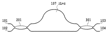
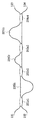
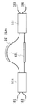
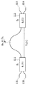
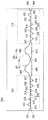
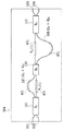
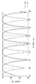
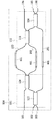
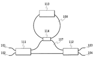
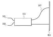
本発明の第1の実施形態における光合分波回路を図4に示す。本回路は、2入力2出力の2個の位相生成光結合器111,112と、これら2個の位相生成光結合器111,112に挟まれた2本の光導波路からなる光路長差付与手段107と、位相生成光結合器111,112に接続するそれぞれ二本の入出力光導波路101,102及び103,104より構成されている。
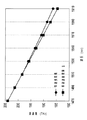
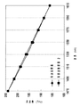
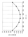
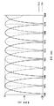
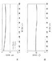
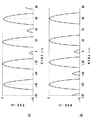
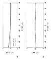
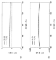
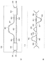
一般的な波長と周波数の関係を図5に示す。CWDMグリッド上の波長に対する周波数を、f=c/λより求め、プロットしたものを「等波長間隔」と示した。但し、fは周波数、cは光速度、λは波長である。また1470nm近傍での周波数間隔Δf1を求め(≒2.74THz)、1470nmにおける周波数を基準に、等しい周波数間隔でCWDMグリッドに対する周波数をプロットしたものを「等周波数間隔1」と示した。
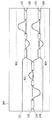
本発明の第2の実施形態における光合分波回路を図14に示す。この回路は、出力位相差が透過帯域の波長に対して各々異なる二つの位相生成光結合器111,112と、これら2個の位相生成光結合器に挟まれた1つの光路長差付与手段107と、位相生成光結合器111,112に接続するそれぞれ二本の入出力光導波路101,102と103,104より構成されている。
本発明の第3の実施形態における合分波回路を図19に示す。この回路は、三つの位相生成光結合器111,112,113と、これら3個の位相生成光結合器に挟まれた2つの光路長差付与手段107,108と、位相生成光結合器111に接続するそれぞれ二本の入出力光導波路101,102と、位相生成光結合器113に接続するそれぞれ二本の入出力光導波路103,104より構成されている。
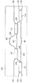
本発明の第4の実施形態における光合分波回路を図22に示す。この回路は、二つの位相生成光結合器111,112と、これら2個の位相生成光結合器に挟まれた1つの光路長差付与手段107と、位相生成光結合器111に接続する入力導波路101,102より構成されている干渉回路において、位相生成光結合器112の二つの出力がアレイ導波路603と、アレイ導波路の両側に設けられた第一スラブ導波路602及び第二スラブ導波路604と、第二スラブ導波路に結合する8つの出力導波路605より構成されるアレイ導波路回折格子の第一スラブ導波路602に入射されている。
本発明の第5の実施形態における光合分波回路を図26に示す。この回路は、前段の位相生成機能を備えた光合分波回路801と、位相生成機能を備えた光合分波回路801の二つの出力にそれぞれ接続された後段の位相生成機能を備えた光合分波回路802,803とにより構成されている。ここで、前段の光合分波回路は波長間隔が20nmの等波長間隔マッハツェンダ干渉回路であり、後段の光合分波回路は波長間隔が40nmの等波長間隔マッハツェンダ干渉回路である。更に、前段と後段の干渉回路で入力光が4つの出力に分波されるように位相が設定されている。
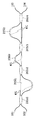
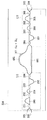
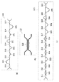
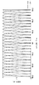
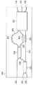
本発明の第6の実施形態の光合分波回路を図28に示す。本回路はN+1個(Nは1以上の整数)の位相生成光結合器111〜115と、隣接する位相生成光結合器に挟まれたN個の光路長差付与手段107〜109と、1個目の位相生成光結合器111に接続された2本の入力導波路101、102と、N+1個目の位相生成光結合器115に接続された2本の出力導波路103、104より構成されるN段ラティス・フィルタである。
で置き換えられる複素変数、Hn*(z)はHn(z)のパラ複素共役であり、上添え字*で表す通常の複素共役を用いて、
はn番目のラティス・フィルタ型位相生成光結合器のp番目の光路長差付与部の光学的光路長差、
はn番目のラティス・フィルタ型位相生成光結合器のp番目の光結合器の結合角であり、より詳しく説明すると波長依存性を有する振幅結合率の角度表示である。
に設定した。もちろん、位相生成光結合器の設計パラメータを導出するのにこれらの制約条件は不要である。また、ラティス・フィルタ型位相生成光結合器の段数を多くするほど、そして制約条件を課さずに任意の設計パラメータを用いることにより、目的とする特性との近似度を高めることができる。しかし最適化により、上記制約条件を与えたとしても十分近似度の高い設計パラメータを導出することができた。さらに、近似しようとする位相関数に変数を導入することにより、位相生成光結合器の設計パラメータに柔軟性を持たせ、より近似を容易にすることができる。
(参考例の第7の実施形態)
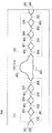
本発明の第7の実施形態における光合分波回路を図36に示す。本回路は、N+1個(N=2)の位相生成光結合器111〜113と、隣接する位相生成光結合器に挟まれたN(N=2)個の光路長差付与手段107〜108と、1個目の位相生成光結合器111に接続された2本の入力導波路101、102と、N+1=3個目の位相生成光結合器113に接続された2本の出力導波路103、104より構成される2段ラティス・フィルタである。
位相生成光結合器111〜113の伝達行列はそれぞれ、
に設定した。
本発明の第8の実施形態における光合分波回路を図42に示す。本回路はN+1個(N=2)の位相生成光結合器111〜113と、隣接する位相生成光結合器に挟まれたN(N=2)個の光路長差付与手段107〜108と、1個目の位相生成光結合器111に接続された2本の入力導波路101、102と、N+1=3個目の位相生成光結合器113に接続された2本の出力導波路103、104より構成される2段ラティス・フィルタである。
に設定した。また、位相生成光結合器111の光路長差付与部231、232、233、234、235、236の光学的光路長差は
に設定した。さらに、位相生成光結合器113の光路長差付与部331、332、333、334、335、336、337、338、339、340の光学的光路長差は
に設定した。
に設定した。また、方向性結合器310の結合角は0.38である。
本発明の各実施形態では主に波長領域で使用する光合分波回路を説明してきたが、本発明の原理は波長領域だけではなく、光周波数領域にも適用することができる。本実施形態では、その具体的な一例を示す。
(msは整数)を満たすなら光周波数間隔Δfと中心光周波数fcを同時に設定することができるが、このような特殊な場合に限られる。
で置き換えられる複素変数である。
はn番目のラティス・フィルタ型位相生成光結合器のp番目の光結合器の結合角であり、より詳しく説明すると光周波数依存性を有する振幅結合率の角度表示である。
の時は位相を、
を満たすので式(32)が有効であり、透過帯の中心位置は光周波数グリッドと完全に一致し、光周波数グリッドからの軸ずれは零であることがわかる。
本発明の各実施形態では主に、M+1個(Mは1以上の整数)の光結合器と隣接する光結合器に挟まれたM個の光路長差付与部により構成されるラティス・フィルタ型の光合分波手段を位相生成手段として用いた。それは、ラティス・フィルタは原理的に損失が無いこと、そしてM+1個の光結合器の分岐比(結合角)とM個の光路長差付与部の光学的光路長差を適切に設定することにより、位相生成光結合器として機能させることができることによる。また、光結合器として、近接した二本の光導波路からなる方向性結合器を用いたのは、方向性結合器の結合長を調整するだけで、結合角を変化させることができるからである。
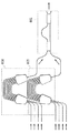
図57に、本発明の第10実施形態の第1変形における位相生成手段を示す。図の光合分波手段114は複数の光合分波手段111、112、113より構成されている。具体的には、光合分波手段111の二つの出力ポートに光合分波手段112、113が縦列接続されている。光合分波手段114は位相生成光結合器であるが、光合分波手段114を構成する光合分波手段111、112、113も位相生成光結合器である。このように、位相生成光結合器として機能する複数の光合分波手段を用いて任意のP入力Q出力(P、Qは自然数)位相生成光結合器を構成してもよい。
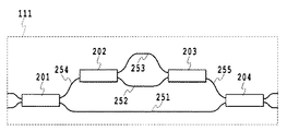
図59に、本発明の第10実施形態の第2変形における位相生成手段を示す。図の位相生成光結合器111は光結合器201〜204と光遅延線251〜255より構成されている。位相生成光結合器111の構成は、広義にはトランスバーサル型光合分波回路と呼ぶことができる。
本発明の第11の実施形態における光合分波回路を図61に示す。本回路はN+1個(Nは1以上の整数)の光結合器211〜215と、隣接する光結合器に挟まれたN個の光路長差付与手段107〜109と、1個目の光結合器211に接続された2本の入力導波路101、102と、N+1個目の光結合器215に接続された2本の出力導波路103、104より構成されるN段ラティス・フィルタである。
本発明の第12の実施形態における光合分波回路を図65に示す。任意の特性を実現できる光遅延線回路としてラティス・フィルタやトランスバーサル・フィルタ等のフィルタ構成が一般に用いられているが、本実施形態で説明する多段マッハツェンダ干渉計も同様に任意の特性を実現できるフィルタ構成の一つである。
図66に、本発明の第13の実施形態における光合分波回路を示す。本回路は一つ以上の入力と二つ以上の出力を持つ位相生成光結合器111、112と、これらの位相生成光結合器に結合される光遅延線251〜253からなる光路長差付与手段により構成される干渉回路であり、広義のトランスバーサル型光合分波回路である。
図68に、本発明の第13実施形態の変形にかかる光合分波回路を示す。本回路は一つ以上の入力と二つ以上の出力を持つ位相生成光結合器111、112と、113、114と、これらの位相生成光結合器に結合される光遅延線251〜255からなる光路長差付与手段により構成される干渉回路であり、広義のトランスバーサル型光合分波回路である。
図71(a)に本発明の第14の実施形態における光合分波回路を示す。本発明の各実施形態で説明した光合分波回路では、作製した回路の偏波依存性が小さかったため、偏波について考慮しなかった。しかし、偏波依存性が大きい場合は偏波を考慮して回路を設計・作製することにより、偏波依存性を解消することができる。反対に、偏波依存性を適切に発生させることにより、例えば偏波インタリーブ・フィルタや偏光ビームスプリッタなど偏波依存性を有する光合分波回路を実現することもできる。
本発明の各実施形態で用いた光遅延線は、主にFIR (Finite Impulse Response)型フィルタであった。例えば、マッハツェンダ干渉計、ラティス・フィルタ、そしてトランスバーサル・フィルタはFIR型フィルタの代表例であり、任意の透過特性を実現できることから、広く用いられている。しかし、FIR型フィルタ以外にもIIR (Infinite Impulse Response)型フィルタがあり、本発明の原理を適用することにより、その光学特性を修正することができる。IIR型フィルタとしてリング共振器を用いた光遅延線回路が知られている。
図75に本発明の第16の実施形態における光合分波回路の構成を示す。本回路は、一つ以上の入力と二つ以上の出力を有する位相生成光結合器111と、位相生成光結合器111に接続される光路長差付与手段107により構成される干渉回路であり、位相生成光結合器111は出力の位相差が波長依存性もしくは光周波数依存性を有する位相生成光結合器として機能させている。
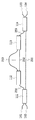
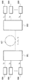
図77に本発明の第17の実施形態における光合分波回路の構成を示す。本回路は、位相生成機能を用いたマッハツェンダ干渉計であり、その光路長差付与手段107の真中に溝が形成され、薄膜812が挿入されている。
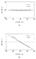
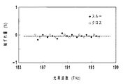
以上述べた各実施形態では、位相生成機能を備えた光合分波回路をシリコン基板上に形成された石英系光導波路を用いて作製したと説明したが(作製例は、非特許文献11を参照)、本発明の合分波回路の構成は光導波路の種類、形状、材料によらない。
201、202、203、204 光結合器
208、209 光結合器
211、212、213、214、215、216、217、218、219、220、221、310、311、312、313、314、315、316、317、318、319、320、321 光結合器
301、302、303、304 光結合器
107、108、109 光路長差付与手段
111、112、113、114、115、116 位相生成光結合器
205、206、207 光路長差付与部
210 光路長差付与手段
231、232、233,234、235、236、237、238、239、240、331、332,333、334、335、336、337、338、339、340 光路長差付与部
251、252、253、254、255 光遅延線
305、306、307 光路長差付与部
401 位相調整手段
411、412 複屈折制御手段
501 上部クラッド
502 コア
503 下部クラッド
504 基板
601 アレイ導波路回折格子の入力導波路
602 第一スラブ導波路
603 アレイ導波路(光路長差付与手段)
604 第二スラブ導波路
605 アレイ導波路回折格子の出力導波路
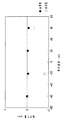
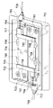
701 筐体
702 ペルチェ保持板
703 固定ねじ
704 PLC(石英系光導波路回路)チップ
705 ガラス板
706 ファイバ
707 ファイバブロック
708 断熱性弾性接着剤
709 ファイバコード
710 ファイバブーツ
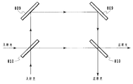
801、802、803 位相生成機能を用いた光合分波回路
804、805 アレイ導波路回折格子
806 送信器
807 ファイバ
808 受信器
809 全反射鏡
810 半透明鏡
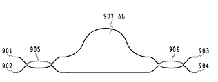
901、902、903、904 入出力導波路
905、906 光結合器
907 光路長差付与手段
Claims (10)
- 複数の透過帯域から構成される全帯域において複数の光を合波分波する光合分波回路において、
入力部と出力部とを有する少なくとも2つの光合分波手段と、
前記少なくとも2つの光合分波手段の間に接続された光路長差付与手段と
を備え、
前記光合分波手段の少なくとも1つは位相生成手段として機能し、前記位相生成手段は、前記出力部の中の2つの出力端から出力される2つの光の位相差として定義される光周波数依存性を持つ位相φを生成し、1つ以上の前記位相生成手段により生成された光周波数の関数によって表され、前記光路長差付与手段に生じさせる光周波数依存性を持つ位相Φが、隣接する前記透過帯域の各中心光周波数の一定の周波数間隔および前記全帯域の中心光周波数を所望の値に同時に設定することを特徴とする光合分波回路。 - 前記全帯域における透過特性が、
Nを光合分波回路の次数、xqを展開係数、fを光周波数、Ψ(f)を光周波数領域グリッド上において隣合う透過帯域間の中心光周波数間隔を設定するために必要な光周波数依存性を持つ目標位相、ΔL´(=ΔL+δL)を屈折率の光周波数依存性を含めた前記光路長差付与手段の光学的光路長差、ΔLを光学的光路長差、δLを微小光学的光路長差とすると、
前記位相生成手段によって生成される光周波数依存性を持つ前記位相Φは、光周波数依存性を持つ前記目標位相Ψに等しいことを特徴とする請求項1に記載の光合分波回路。 - 光周波数依存性を持つ前記位相Φは、前記光合分波回路の前記全帯域における光周波数(f)の関数によって与えられ、前記関数は2次関数以上の多項式であって、光周波数依存性を持つ前記目標位相Ψは、
Δfを光周波数領域グリッド上における合分波回路の光周波数間隔、fcを光合分波回路の全帯域の中心近傍に位置する透過帯域の中心光周波数、mを整数とすると、
- 前記位相生成手段は、(M+1)個(Mは2以上の整数)の光結合器と、隣合う前記光結合器の間に配置されたM個の光路長差付与部とから構成されており、前記光周波数依存性を持つ位相は、前記光結合器の振幅結合率および前記光路長差付与部の光学的光路長差をそれぞれ最適化することによって生成されることを特徴とする請求項1に記載の光合分波回路。
- 前記位相生成手段は、(M+1)個(Mは2以上の整数)の光結合器と、隣合う前記光結合器の間に配置されたM個の光路長差付与部とから構成されており、光周波数依存性を持つ前記位相Φが光周波数依存性を持つ前記目標位相Ψに等しく成るように、前記光結合器の振幅結合率および前記光路長差付与部の光学的光路長差ならびに前記光合分波回路が備える前記光路長差付与手段に付加する光学的光路長差δLの各々が設定されることを特徴とする請求項2に記載の光合分波回路。
- 前記光合分波回路は光干渉回路であり、
前記光干渉回路は、(N+1)個(Nは1以上の整数)の前記光合分波手段と、隣合う前記光合分波手段の間に配置されたN個の前記光路長差付与手段とを接続して構成されていることを特徴とする請求項1乃至5のいずれかに記載の光合分波回路。 - 前記光合分波回路は、2つの前記光合分波手段と、前記2つの光合分波手段の間に配置された前記光路長差付与手段と、前記光合分波手段の一方に接続された少なくとも1本の入力導波路および前記光合分波手段の他方に接続された複数本の出力導波路と、を備えたマッハツェンダ干渉回路であり、
前記2つの光合分波手段のいずれか一方は、位相生成手段を備えた位相生成光結合器であり、
前記位相生成光結合器は、(M+1)個(Mは2以上の整数)の光結合器と、隣合う前記光結合器の間に配置されたM個の光路長差付与部と、によって構成されていることを特徴とする請求項6に記載の光合分波回路。 - 複数の透過帯域から構成される全帯域において複数の光を合波分波する光合分波回路において、
入力部と出力部とを有する少なくとも1つの光合分波手段と、
前記少なくとも1つの光合分波手段の前記出力部に光学的に接続された光路長差付与手段と、
前記光路長差付与手段に接続された反射板と、
を備え、前記反射板を信号光の折り返し点とする反射型の光合分波回路であって、
前記光合分波手段の少なくとも1つは位相生成手段として機能し、前記位相生成手段は、前記出力部の中の2つの出力端から出力される2つの光の位相差として定義される光周波数依存性を持つ位相φを生成し、1つ以上の前記位相生成手段により生成された光周波数の関数によって表され、前記光路長差付与手段に生じさせる光周波数依存性を持つ位相Φが、隣接する前記透過帯域の各中心光周波数の一定間隔および前記全帯域の中心光周波数を所望の値に同時に設定することを特徴とする光合分波回路。 - 複数の透過帯域から構成される全帯域において複数の光を合波分波する光合分波回路の設計方法であって、前記光合分波回路は、入力部と出力部とを有する少なくとも2つの光合分波手段と、前記少なくとも2つの光合分波手段の間に接続された光路長差付与手段とを備え、
前記光合分波手段の少なくとも1つは位相生成手段として機能し、前記位相生成手段は、前記出力部の中の2つの出力端から出力される2つの光の位相差として定義される光周波数依存性を持つ位相φを生成し、前記方法は、
光周波数依存性を持つ目標位相Ψを決定するステップであって、前記目標位相Ψは、隣接する前記透過帯域の各中心光周波数の一定の光周波数間隔および前記全帯域の中心光周波数を所望の値に同時に設定するのに必要な位相であるステップと、
1つ以上の前記位相生成手段により生成された光周波数の関数によって表され、前記光路長差付与手段に生じさせる光周波数依存性を持つ位相Φが、光周波数依存性を持つ前記目標位相Ψ(f)に等しくなるように前記位相生成手段を構成するステップと
を備えることを特徴とする設計方法。 - 光周波数依存性を持つ目標位相Ψを決定する前記ステップは、
前記全帯域における透過特性が、
Nを光合分波回路の次数、xqを展開係数、fを光周波数、Ψ(f)を光周波数領域グリッド上において隣合う透過帯域間の中心光周波数間隔を設定するために必要な光周波数依存性を持つ目標位相、ΔL´(=ΔL+δL)を屈折率の光周波数依存性を含めた前記光路長差付与手段の光学的光路長差、ΔLを光学的光路長差、δLを微小光学的光路長差とすると、
Priority Applications (1)
| Application Number | Priority Date | Filing Date | Title |
|---|---|---|---|
| JP2008146281A JP4494495B2 (ja) | 2002-12-06 | 2008-06-03 | 位相生成機能を備えた光合分波回路 |
Applications Claiming Priority (2)
| Application Number | Priority Date | Filing Date | Title |
|---|---|---|---|
| JP2002354640 | 2002-12-06 | ||
| JP2008146281A JP4494495B2 (ja) | 2002-12-06 | 2008-06-03 | 位相生成機能を備えた光合分波回路 |
Related Parent Applications (1)
| Application Number | Title | Priority Date | Filing Date |
|---|---|---|---|
| JP2003402235A Division JP4152869B2 (ja) | 2002-12-06 | 2003-12-01 | 位相生成機能を備えた光合分波回路 |
Publications (2)
| Publication Number | Publication Date |
|---|---|
| JP2008209955A JP2008209955A (ja) | 2008-09-11 |
| JP4494495B2 true JP4494495B2 (ja) | 2010-06-30 |
Family
ID=32310755
Family Applications (1)
| Application Number | Title | Priority Date | Filing Date |
|---|---|---|---|
| JP2008146281A Expired - Lifetime JP4494495B2 (ja) | 2002-12-06 | 2008-06-03 | 位相生成機能を備えた光合分波回路 |
Country Status (5)
| Country | Link |
|---|---|
| US (1) | US7085438B2 (ja) |
| EP (2) | EP1830207B1 (ja) |
| JP (1) | JP4494495B2 (ja) |
| CN (1) | CN1508997B (ja) |
| DE (1) | DE60314829T2 (ja) |
Families Citing this family (39)
| Publication number | Priority date | Publication date | Assignee | Title |
|---|---|---|---|---|
| JP4351937B2 (ja) * | 2004-03-17 | 2009-10-28 | 成田国際空港株式会社 | 路面凍結検出センサ、路面凍結検出センサの設置方法および路面凍結検出方法 |
| JP4196407B2 (ja) * | 2004-06-30 | 2008-12-17 | 横河電機株式会社 | 可変光信号遅延器およびこれを用いた可変光信号遅延装置 |
| US7590358B2 (en) * | 2005-02-28 | 2009-09-15 | Vladimir Grigoryan | Optical regenerative amplifier for binary phase shift-keying signals |
| JP2006284955A (ja) * | 2005-03-31 | 2006-10-19 | Nec Corp | 光波長合分波器 |
| EP1966921A1 (en) * | 2005-12-28 | 2008-09-10 | Pirelli & C. S.p.A. | Method and device for tunable optical filtering |
| US8923700B2 (en) * | 2005-12-28 | 2014-12-30 | Google Inc. | Method and system for tunable optical filtering |
| CN101454702B (zh) * | 2006-02-24 | 2011-03-09 | 尼奥弗托尼克斯公司 | 宽带2×2光分路器 |
| JP2008004633A (ja) * | 2006-06-20 | 2008-01-10 | Nec Corp | 光モジュール及び実装方法 |
| US7433549B2 (en) * | 2006-09-20 | 2008-10-07 | Lucent Technologies Inc. | Optical modulator |
| US7684666B2 (en) * | 2006-11-10 | 2010-03-23 | International Business Machines Corporation | Method and apparatus for tuning an optical delay line |
| US7496253B2 (en) * | 2006-12-07 | 2009-02-24 | Industrial Technology Research Institute | Wide passband optical interleaver |
| JP2008224313A (ja) * | 2007-03-09 | 2008-09-25 | Yokogawa Electric Corp | 干渉計及び復調器 |
| DE102007031864A1 (de) * | 2007-07-04 | 2009-01-15 | Fraunhofer-Gesellschaft zur Förderung der angewandten Forschung e.V. | Verfahren und Anordnung zur Kompensation von polarisationsabhängiger Frequenzverschiebung (PDFS) in optischen Wellenleitern sowie ein entsprechendes Computerprogramm und ein entsprechendes computerlesbares Speichermedium |
| US7519240B1 (en) * | 2007-07-17 | 2009-04-14 | Infinera Corporation | Multi-section coupler to mitigate guide-guide asymmetry |
| US7555178B2 (en) * | 2007-07-20 | 2009-06-30 | Infinera Corporation | Periodic optical filter |
| JP5457661B2 (ja) * | 2008-07-14 | 2014-04-02 | 日本電信電話株式会社 | 光波長合分波回路 |
| JP5399693B2 (ja) * | 2008-07-14 | 2014-01-29 | 日本電信電話株式会社 | 光波長合分波回路 |
| US8224139B2 (en) * | 2008-08-21 | 2012-07-17 | Infinera Corporation | Tunable optical filter |
| US8270792B1 (en) * | 2009-09-15 | 2012-09-18 | Hrl Laboratories, Llc | High-resolution multi-level frequency channelizers |
| EP2479593B1 (en) * | 2009-09-18 | 2015-07-29 | Nippon Telegraph And Telephone Corporation | Optical multiplexer/demultiplexer circuit |
| JP2012119836A (ja) * | 2010-11-30 | 2012-06-21 | Fuji Xerox Co Ltd | 送信装置及び送受信装置 |
| JP2012215692A (ja) * | 2011-03-31 | 2012-11-08 | Furukawa Electric Co Ltd:The | 偏波分離素子および光集積素子 |
| US10009106B2 (en) * | 2012-05-14 | 2018-06-26 | Acacia Communications, Inc. | Silicon photonics multicarrier optical transceiver |
| US10534189B2 (en) * | 2012-11-27 | 2020-01-14 | The Board Of Trustees Of The Leland Stanford Junior University | Universal linear components |
| US9207399B2 (en) | 2013-01-28 | 2015-12-08 | Aurrion, Inc. | Athermal optical filter with active tuning and simplified control |
| US9354389B2 (en) * | 2013-03-20 | 2016-05-31 | Effect Photonics B.V. | Integrated photonic component and method of designing the same |
| US20140293393A1 (en) * | 2013-03-28 | 2014-10-02 | Barthelemy Fondeur | Flat-top tunable filter |
| US20150124845A1 (en) * | 2013-11-06 | 2015-05-07 | Aurrion, Inc. | Optical mode steering for wavelength stabilization |
| JP6446803B2 (ja) * | 2014-03-25 | 2019-01-09 | 日本電気株式会社 | 光送受信器 |
| US9438263B1 (en) | 2014-05-02 | 2016-09-06 | Hrl Laboratories, Llc | Controllable opto-electronic time stretcher, an electro-optical analog to digital converter having non-uniform sampling using the same, and related methods of operation |
| JP6383590B2 (ja) * | 2014-07-07 | 2018-08-29 | 富士通株式会社 | 光受信装置 |
| JP6428146B2 (ja) * | 2014-10-22 | 2018-11-28 | 日本電気株式会社 | 光導波路デバイス及びその製造方法 |
| CN111208605B (zh) | 2015-07-24 | 2023-01-17 | 瞻博网络公司 | 波导阵列中的相位调谐 |
| IT201700053579A1 (it) * | 2017-05-17 | 2018-11-17 | Milano Politecnico | Metodo e sistema di ritardo ottico |
| CN109283616B (zh) * | 2018-12-10 | 2023-09-12 | 中国科学院上海微系统与信息技术研究所 | 温度不敏感马赫曾德尔干涉仪 |
| JP7279518B2 (ja) * | 2019-05-29 | 2023-05-23 | 富士通株式会社 | 光分波器、光伝送装置及び光分波制御方法 |
| JP7415715B2 (ja) | 2020-03-24 | 2024-01-17 | 富士通株式会社 | 光通信素子、光送信器及び制御方法 |
| TWI740621B (zh) * | 2020-08-26 | 2021-09-21 | 國立臺灣科技大學 | 推拉式可調光延遲線 |
| US20230021995A1 (en) * | 2021-07-06 | 2023-01-26 | Psiquantum, Corp. | Mach zehnder lattice based generalized mach zehnder interferometer |
Citations (4)
| Publication number | Priority date | Publication date | Assignee | Title |
|---|---|---|---|---|
| JP2000347148A (ja) * | 1999-06-09 | 2000-12-15 | Nippon Telegr & Teleph Corp <Ntt> | ハーフバンド光信号処理器 |
| JP2001249237A (ja) * | 2000-03-03 | 2001-09-14 | Hitachi Cable Ltd | 光合分波器 |
| JP2002082241A (ja) * | 2000-06-28 | 2002-03-22 | Nippon Telegr & Teleph Corp <Ntt> | 光合分波器 |
| JP2002318376A (ja) * | 2001-02-07 | 2002-10-31 | Nippon Telegr & Teleph Corp <Ntt> | 光分波器および光合波器 |
Family Cites Families (20)
| Publication number | Priority date | Publication date | Assignee | Title |
|---|---|---|---|---|
| GB2144868B (en) * | 1983-08-09 | 1987-01-14 | Standard Telephones Cables Ltd | Integrated optic arrangement |
| US5044715A (en) | 1989-02-07 | 1991-09-03 | Nippon Telegraph And Telephone Corporation | Guided-wave optical branching components and optical switches |
| JP2518939B2 (ja) | 1989-12-04 | 1996-07-31 | 積水化学工業株式会社 | 話者照合システム |
| US5488680A (en) | 1994-08-24 | 1996-01-30 | At&T Corp. | Frequency routing device having a wide and substantially flat passband |
| US5596661A (en) | 1994-12-28 | 1997-01-21 | Lucent Technologies Inc. | Monolithic optical waveguide filters based on Fourier expansion |
| JPH11109147A (ja) | 1997-10-01 | 1999-04-23 | Nippon Telegr & Teleph Corp <Ntt> | アレイ導波路格子素子 |
| AUPP208398A0 (en) * | 1998-03-02 | 1998-03-26 | University Of Melbourne, The | An optical device for dispersion compensation |
| JP2001094625A (ja) * | 1999-09-27 | 2001-04-06 | Canon Inc | データ通信装置、データ通信方法及び記憶媒体 |
| US6289147B1 (en) * | 1999-11-01 | 2001-09-11 | Bbv Design Bv | Passband flattening of a phasar |
| DE60040424D1 (de) * | 2000-01-06 | 2008-11-13 | Nippon Telegraph & Telephone | CDMA Kodierer-Dekodierer, CDMA Nachrichtenübertragungssystem und WDM-CDMA Nachrichtenübertragungssystem |
| US6907156B1 (en) | 2000-05-17 | 2005-06-14 | Lucent Technologies Inc. | Reconfigurable multi-channel filters having enhanced channel bandwidth |
| EP1168010B1 (en) | 2000-06-28 | 2006-08-16 | Nippon Telegraph and Telephone Corporation | Optical multi/demultiplexer |
| JP3630085B2 (ja) * | 2000-09-14 | 2005-03-16 | 日本電気株式会社 | アレイ導波路回折格子素子の製造方法およびアレイ導波路回折格子素子 |
| US20020044712A1 (en) | 2000-10-16 | 2002-04-18 | Henry Hung | Apparatus for adding wavelength components in wavelength division multiplexed optical signals using mach-zehnder interferometer |
| US7043100B2 (en) | 2001-01-25 | 2006-05-09 | E. I. Du Pont De Nemours And Company | Polarization independent waveguide optical isolator and circulator |
| US6735358B2 (en) | 2001-02-07 | 2004-05-11 | Nippon Telegraph And Telephone Corporation | Optical multiplexer and optical demultiplexer |
| US6763154B2 (en) | 2001-05-21 | 2004-07-13 | Jds Uniphase Inc. | Methods and structures for the control of optical waveguide devices by stress |
| US6892021B2 (en) * | 2001-09-17 | 2005-05-10 | Lucent Technologies Inc. | Dynamic gain equalization arrangement for optical signals |
| EP1296471A3 (de) * | 2001-09-25 | 2005-06-01 | Siemens Aktiengesellschaft | Kompensationsanordnung zur adaptiven Entzerrung eines optischen Signals |
| US6804431B2 (en) * | 2002-07-15 | 2004-10-12 | Stratos Lightwave, Inc. | Pluggable optical transceiver array having wavelength division multiplexing and demultiplexing features |
-
2003
- 2003-12-03 US US10/727,171 patent/US7085438B2/en not_active Expired - Fee Related
- 2003-12-04 EP EP07107515.4A patent/EP1830207B1/en not_active Expired - Fee Related
- 2003-12-04 DE DE60314829T patent/DE60314829T2/de not_active Expired - Lifetime
- 2003-12-04 EP EP03027949A patent/EP1426800B1/en not_active Expired - Fee Related
- 2003-12-08 CN CN200310118258.3A patent/CN1508997B/zh not_active Expired - Fee Related
-
2008
- 2008-06-03 JP JP2008146281A patent/JP4494495B2/ja not_active Expired - Lifetime
Patent Citations (4)
| Publication number | Priority date | Publication date | Assignee | Title |
|---|---|---|---|---|
| JP2000347148A (ja) * | 1999-06-09 | 2000-12-15 | Nippon Telegr & Teleph Corp <Ntt> | ハーフバンド光信号処理器 |
| JP2001249237A (ja) * | 2000-03-03 | 2001-09-14 | Hitachi Cable Ltd | 光合分波器 |
| JP2002082241A (ja) * | 2000-06-28 | 2002-03-22 | Nippon Telegr & Teleph Corp <Ntt> | 光合分波器 |
| JP2002318376A (ja) * | 2001-02-07 | 2002-10-31 | Nippon Telegr & Teleph Corp <Ntt> | 光分波器および光合波器 |
Also Published As
| Publication number | Publication date |
|---|---|
| EP1426800A3 (en) | 2005-01-12 |
| EP1830207B1 (en) | 2013-06-05 |
| US20040136647A1 (en) | 2004-07-15 |
| CN1508997B (zh) | 2010-05-05 |
| EP1830207A3 (en) | 2007-09-12 |
| CN1508997A (zh) | 2004-06-30 |
| EP1426800A2 (en) | 2004-06-09 |
| EP1426800B1 (en) | 2007-07-11 |
| DE60314829T2 (de) | 2008-03-13 |
| US7085438B2 (en) | 2006-08-01 |
| DE60314829D1 (de) | 2007-08-23 |
| JP2008209955A (ja) | 2008-09-11 |
| EP1830207A2 (en) | 2007-09-05 |
Similar Documents
| Publication | Publication Date | Title |
|---|---|---|
| JP4494495B2 (ja) | 位相生成機能を備えた光合分波回路 | |
| KR100725638B1 (ko) | 간섭계형 광 스위치 및 가변 광 감쇠기 | |
| Cao et al. | Interleaver technology: comparisons and applications requirements | |
| US7492983B2 (en) | Optical circuit device | |
| EP1286192B1 (en) | Optical waveguide filter | |
| JP4152869B2 (ja) | 位相生成機能を備えた光合分波回路 | |
| JP2003035830A (ja) | 光波長合分波器 | |
| US6304380B1 (en) | Reducing polarization dependency of optical apparatus | |
| US20020085252A1 (en) | Interleaver filters employing non-birefringent elements | |
| US6845191B1 (en) | Optical filter for wavelength division multipled optical signals | |
| US6324322B1 (en) | Fused-fiber multi-window wavelength filter using unbalanced Michelson Interferometer | |
| JP4197126B2 (ja) | 光スイッチ及び光波長ルータ | |
| JP4263027B2 (ja) | 導波路型光信号処理器 | |
| JP4934625B2 (ja) | Plc型可変分散補償器 | |
| US20060002653A1 (en) | Apparatus for an optical circuit having a flat wavelength response | |
| JP2000147280A (ja) | 光合分波器の波長補正方法 | |
| de Ridder et al. | Interleavers | |
| Kokubun | Waveguide filters and related technologies: issues and solutions for practical use in transmission systems | |
| Jeong | Flat-spectral-band filter for fabrication tolerance and wideband spectral range | |
| Mizuno et al. | Uniform wavelength spacing Mach-Zehnder interferometer using phase-generating couplers | |
| Chiba et al. | Waveguide interleaving filters | |
| JP4799602B2 (ja) | 導波路型光信号処理器 | |
| Mizuno et al. | Interleave filter based on coherent optical transversal filter | |
| Li | Planar waveguide WDM technology: From components to systems | |
| KR20050040522A (ko) | 전광섬유형 인터리버 소자의 온도 안정화 및 그 제조방법 |
Legal Events
| Date | Code | Title | Description |
|---|---|---|---|
| A131 | Notification of reasons for refusal |
Free format text: JAPANESE INTERMEDIATE CODE: A131 Effective date: 20100115 |
|
| RD13 | Notification of appointment of power of sub attorney |
Free format text: JAPANESE INTERMEDIATE CODE: A7433 Effective date: 20100222 |
|
| A521 | Request for written amendment filed |
Free format text: JAPANESE INTERMEDIATE CODE: A821 Effective date: 20100222 |
|
| A521 | Request for written amendment filed |
Free format text: JAPANESE INTERMEDIATE CODE: A523 Effective date: 20100316 |
|
| TRDD | Decision of grant or rejection written | ||
| A01 | Written decision to grant a patent or to grant a registration (utility model) |
Free format text: JAPANESE INTERMEDIATE CODE: A01 Effective date: 20100402 |
|
| A01 | Written decision to grant a patent or to grant a registration (utility model) |
Free format text: JAPANESE INTERMEDIATE CODE: A01 |
|
| A61 | First payment of annual fees (during grant procedure) |
Free format text: JAPANESE INTERMEDIATE CODE: A61 Effective date: 20100407 |
|
| FPAY | Renewal fee payment (event date is renewal date of database) |
Free format text: PAYMENT UNTIL: 20130416 Year of fee payment: 3 |
|
| FPAY | Renewal fee payment (event date is renewal date of database) |
Free format text: PAYMENT UNTIL: 20140416 Year of fee payment: 4 |
|
| S531 | Written request for registration of change of domicile |
Free format text: JAPANESE INTERMEDIATE CODE: R313531 |
|
| R350 | Written notification of registration of transfer |
Free format text: JAPANESE INTERMEDIATE CODE: R350 |