JP4494495B2 - Optical multiplexing / demultiplexing circuit with phase generation function - Google Patents
Optical multiplexing / demultiplexing circuit with phase generation function Download PDFInfo
- Publication number
- JP4494495B2 JP4494495B2 JP2008146281A JP2008146281A JP4494495B2 JP 4494495 B2 JP4494495 B2 JP 4494495B2 JP 2008146281 A JP2008146281 A JP 2008146281A JP 2008146281 A JP2008146281 A JP 2008146281A JP 4494495 B2 JP4494495 B2 JP 4494495B2
- Authority
- JP
- Japan
- Prior art keywords
- optical
- phase
- path length
- multiplexing
- length difference
- Prior art date
- Legal status (The legal status is an assumption and is not a legal conclusion. Google has not performed a legal analysis and makes no representation as to the accuracy of the status listed.)
- Expired - Lifetime
Links
- 230000003287 optical effect Effects 0.000 title claims description 1858
- 230000005540 biological transmission Effects 0.000 claims description 143
- 230000008878 coupling Effects 0.000 claims description 92
- 238000010168 coupling process Methods 0.000 claims description 92
- 238000005859 coupling reaction Methods 0.000 claims description 92
- 238000013461 design Methods 0.000 claims description 38
- 238000000034 method Methods 0.000 claims description 29
- 238000012887 quadratic function Methods 0.000 claims description 5
- 238000010586 diagram Methods 0.000 description 43
- 238000004519 manufacturing process Methods 0.000 description 27
- 230000010287 polarization Effects 0.000 description 25
- 238000012937 correction Methods 0.000 description 22
- 239000010409 thin film Substances 0.000 description 22
- 239000000835 fiber Substances 0.000 description 19
- VYPSYNLAJGMNEJ-UHFFFAOYSA-N Silicium dioxide Chemical compound O=[Si]=O VYPSYNLAJGMNEJ-UHFFFAOYSA-N 0.000 description 17
- 239000000758 substrate Substances 0.000 description 15
- XUIMIQQOPSSXEZ-UHFFFAOYSA-N Silicon Chemical compound [Si] XUIMIQQOPSSXEZ-UHFFFAOYSA-N 0.000 description 11
- 230000001419 dependent effect Effects 0.000 description 11
- 238000005457 optimization Methods 0.000 description 11
- 229910052710 silicon Inorganic materials 0.000 description 11
- 239000010703 silicon Substances 0.000 description 11
- 239000000463 material Substances 0.000 description 10
- 238000012546 transfer Methods 0.000 description 9
- 238000000151 deposition Methods 0.000 description 8
- 230000000694 effects Effects 0.000 description 8
- 238000000206 photolithography Methods 0.000 description 8
- 238000001020 plasma etching Methods 0.000 description 8
- 230000004048 modification Effects 0.000 description 7
- 238000012986 modification Methods 0.000 description 7
- 230000009466 transformation Effects 0.000 description 7
- 239000000377 silicon dioxide Substances 0.000 description 6
- 230000008859 change Effects 0.000 description 5
- 238000004891 communication Methods 0.000 description 5
- 230000008021 deposition Effects 0.000 description 5
- 238000003780 insertion Methods 0.000 description 5
- 230000037431 insertion Effects 0.000 description 5
- 239000011159 matrix material Substances 0.000 description 5
- 239000013307 optical fiber Substances 0.000 description 5
- 238000000411 transmission spectrum Methods 0.000 description 5
- 239000000853 adhesive Substances 0.000 description 4
- 230000001070 adhesive effect Effects 0.000 description 4
- 238000002939 conjugate gradient method Methods 0.000 description 4
- 230000000737 periodic effect Effects 0.000 description 4
- 239000010453 quartz Substances 0.000 description 4
- 238000002834 transmittance Methods 0.000 description 4
- 230000008033 biological extinction Effects 0.000 description 3
- 238000004364 calculation method Methods 0.000 description 3
- 230000004044 response Effects 0.000 description 3
- 230000008901 benefit Effects 0.000 description 2
- 238000005253 cladding Methods 0.000 description 2
- 239000006185 dispersion Substances 0.000 description 2
- 239000011521 glass Substances 0.000 description 2
- 238000010438 heat treatment Methods 0.000 description 2
- 230000007246 mechanism Effects 0.000 description 2
- 230000008569 process Effects 0.000 description 2
- 230000000644 propagated effect Effects 0.000 description 2
- 230000000087 stabilizing effect Effects 0.000 description 2
- NAWXUBYGYWOOIX-SFHVURJKSA-N (2s)-2-[[4-[2-(2,4-diaminoquinazolin-6-yl)ethyl]benzoyl]amino]-4-methylidenepentanedioic acid Chemical compound C1=CC2=NC(N)=NC(N)=C2C=C1CCC1=CC=C(C(=O)N[C@@H](CC(=C)C(O)=O)C(O)=O)C=C1 NAWXUBYGYWOOIX-SFHVURJKSA-N 0.000 description 1
- 229910003327 LiNbO3 Inorganic materials 0.000 description 1
- 239000004642 Polyimide Substances 0.000 description 1
- 238000005229 chemical vapour deposition Methods 0.000 description 1
- 239000004020 conductor Substances 0.000 description 1
- 230000007423 decrease Effects 0.000 description 1
- 238000009792 diffusion process Methods 0.000 description 1
- 239000002019 doping agent Substances 0.000 description 1
- 238000005516 engineering process Methods 0.000 description 1
- 239000010408 film Substances 0.000 description 1
- 238000010884 ion-beam technique Methods 0.000 description 1
- 150000002500 ions Chemical class 0.000 description 1
- JCCNYMKQOSZNPW-UHFFFAOYSA-N loratadine Chemical compound C1CN(C(=O)OCC)CCC1=C1C2=NC=CC=C2CCC2=CC(Cl)=CC=C21 JCCNYMKQOSZNPW-UHFFFAOYSA-N 0.000 description 1
- 238000005259 measurement Methods 0.000 description 1
- 229920001721 polyimide Polymers 0.000 description 1
- 230000008929 regeneration Effects 0.000 description 1
- 238000011069 regeneration method Methods 0.000 description 1
- 239000011347 resin Substances 0.000 description 1
- 229920005989 resin Polymers 0.000 description 1
- 239000004065 semiconductor Substances 0.000 description 1
- 238000003980 solgel method Methods 0.000 description 1
- 238000004528 spin coating Methods 0.000 description 1
- 238000004544 sputter deposition Methods 0.000 description 1
- 230000006641 stabilisation Effects 0.000 description 1
- 238000011105 stabilization Methods 0.000 description 1
Images


Classifications
-
- G—PHYSICS
- G02—OPTICS
- G02B—OPTICAL ELEMENTS, SYSTEMS OR APPARATUS
- G02B6/00—Light guides; Structural details of arrangements comprising light guides and other optical elements, e.g. couplings
- G02B6/10—Light guides; Structural details of arrangements comprising light guides and other optical elements, e.g. couplings of the optical waveguide type
- G02B6/12—Light guides; Structural details of arrangements comprising light guides and other optical elements, e.g. couplings of the optical waveguide type of the integrated circuit kind
- G02B6/12007—Light guides; Structural details of arrangements comprising light guides and other optical elements, e.g. couplings of the optical waveguide type of the integrated circuit kind forming wavelength selective elements, e.g. multiplexer, demultiplexer
- G02B6/12009—Light guides; Structural details of arrangements comprising light guides and other optical elements, e.g. couplings of the optical waveguide type of the integrated circuit kind forming wavelength selective elements, e.g. multiplexer, demultiplexer comprising arrayed waveguide grating [AWG] devices, i.e. with a phased array of waveguides
- G02B6/12019—Light guides; Structural details of arrangements comprising light guides and other optical elements, e.g. couplings of the optical waveguide type of the integrated circuit kind forming wavelength selective elements, e.g. multiplexer, demultiplexer comprising arrayed waveguide grating [AWG] devices, i.e. with a phased array of waveguides characterised by the optical interconnection to or from the AWG devices, e.g. integration or coupling with lasers or photodiodes
-
- G—PHYSICS
- G02—OPTICS
- G02B—OPTICAL ELEMENTS, SYSTEMS OR APPARATUS
- G02B6/00—Light guides; Structural details of arrangements comprising light guides and other optical elements, e.g. couplings
- G02B6/10—Light guides; Structural details of arrangements comprising light guides and other optical elements, e.g. couplings of the optical waveguide type
- G02B6/12—Light guides; Structural details of arrangements comprising light guides and other optical elements, e.g. couplings of the optical waveguide type of the integrated circuit kind
- G02B6/12007—Light guides; Structural details of arrangements comprising light guides and other optical elements, e.g. couplings of the optical waveguide type of the integrated circuit kind forming wavelength selective elements, e.g. multiplexer, demultiplexer
- G02B6/12009—Light guides; Structural details of arrangements comprising light guides and other optical elements, e.g. couplings of the optical waveguide type of the integrated circuit kind forming wavelength selective elements, e.g. multiplexer, demultiplexer comprising arrayed waveguide grating [AWG] devices, i.e. with a phased array of waveguides
- G02B6/12016—Light guides; Structural details of arrangements comprising light guides and other optical elements, e.g. couplings of the optical waveguide type of the integrated circuit kind forming wavelength selective elements, e.g. multiplexer, demultiplexer comprising arrayed waveguide grating [AWG] devices, i.e. with a phased array of waveguides characterised by the input or output waveguides, e.g. tapered waveguide ends, coupled together pairs of output waveguides
-
- G—PHYSICS
- G02—OPTICS
- G02B—OPTICAL ELEMENTS, SYSTEMS OR APPARATUS
- G02B6/00—Light guides; Structural details of arrangements comprising light guides and other optical elements, e.g. couplings
- G02B6/10—Light guides; Structural details of arrangements comprising light guides and other optical elements, e.g. couplings of the optical waveguide type
- G02B6/12—Light guides; Structural details of arrangements comprising light guides and other optical elements, e.g. couplings of the optical waveguide type of the integrated circuit kind
- G02B6/12007—Light guides; Structural details of arrangements comprising light guides and other optical elements, e.g. couplings of the optical waveguide type of the integrated circuit kind forming wavelength selective elements, e.g. multiplexer, demultiplexer
- G02B6/12009—Light guides; Structural details of arrangements comprising light guides and other optical elements, e.g. couplings of the optical waveguide type of the integrated circuit kind forming wavelength selective elements, e.g. multiplexer, demultiplexer comprising arrayed waveguide grating [AWG] devices, i.e. with a phased array of waveguides
- G02B6/12019—Light guides; Structural details of arrangements comprising light guides and other optical elements, e.g. couplings of the optical waveguide type of the integrated circuit kind forming wavelength selective elements, e.g. multiplexer, demultiplexer comprising arrayed waveguide grating [AWG] devices, i.e. with a phased array of waveguides characterised by the optical interconnection to or from the AWG devices, e.g. integration or coupling with lasers or photodiodes
- G02B6/12021—Comprising cascaded AWG devices; AWG multipass configuration; Plural AWG devices integrated on a single chip
-
- G—PHYSICS
- G02—OPTICS
- G02B—OPTICAL ELEMENTS, SYSTEMS OR APPARATUS
- G02B6/00—Light guides; Structural details of arrangements comprising light guides and other optical elements, e.g. couplings
- G02B6/10—Light guides; Structural details of arrangements comprising light guides and other optical elements, e.g. couplings of the optical waveguide type
- G02B6/12—Light guides; Structural details of arrangements comprising light guides and other optical elements, e.g. couplings of the optical waveguide type of the integrated circuit kind
- G02B6/12007—Light guides; Structural details of arrangements comprising light guides and other optical elements, e.g. couplings of the optical waveguide type of the integrated circuit kind forming wavelength selective elements, e.g. multiplexer, demultiplexer
- G02B6/12009—Light guides; Structural details of arrangements comprising light guides and other optical elements, e.g. couplings of the optical waveguide type of the integrated circuit kind forming wavelength selective elements, e.g. multiplexer, demultiplexer comprising arrayed waveguide grating [AWG] devices, i.e. with a phased array of waveguides
- G02B6/12023—Light guides; Structural details of arrangements comprising light guides and other optical elements, e.g. couplings of the optical waveguide type of the integrated circuit kind forming wavelength selective elements, e.g. multiplexer, demultiplexer comprising arrayed waveguide grating [AWG] devices, i.e. with a phased array of waveguides characterised by means for reducing the polarisation dependence, e.g. reduced birefringence
-
- G—PHYSICS
- G02—OPTICS
- G02B—OPTICAL ELEMENTS, SYSTEMS OR APPARATUS
- G02B6/00—Light guides; Structural details of arrangements comprising light guides and other optical elements, e.g. couplings
- G02B6/24—Coupling light guides
- G02B6/26—Optical coupling means
- G02B6/28—Optical coupling means having data bus means, i.e. plural waveguides interconnected and providing an inherently bidirectional system by mixing and splitting signals
- G02B6/293—Optical coupling means having data bus means, i.e. plural waveguides interconnected and providing an inherently bidirectional system by mixing and splitting signals with wavelength selective means
- G02B6/29346—Optical coupling means having data bus means, i.e. plural waveguides interconnected and providing an inherently bidirectional system by mixing and splitting signals with wavelength selective means operating by wave or beam interference
- G02B6/2935—Mach-Zehnder configuration, i.e. comprising separate splitting and combining means
- G02B6/29352—Mach-Zehnder configuration, i.e. comprising separate splitting and combining means in a light guide
- G02B6/29353—Mach-Zehnder configuration, i.e. comprising separate splitting and combining means in a light guide with a wavelength selective element in at least one light guide interferometer arm, e.g. grating, interference filter, resonator
-
- G—PHYSICS
- G02—OPTICS
- G02B—OPTICAL ELEMENTS, SYSTEMS OR APPARATUS
- G02B6/00—Light guides; Structural details of arrangements comprising light guides and other optical elements, e.g. couplings
- G02B6/24—Coupling light guides
- G02B6/26—Optical coupling means
- G02B6/28—Optical coupling means having data bus means, i.e. plural waveguides interconnected and providing an inherently bidirectional system by mixing and splitting signals
- G02B6/293—Optical coupling means having data bus means, i.e. plural waveguides interconnected and providing an inherently bidirectional system by mixing and splitting signals with wavelength selective means
- G02B6/29346—Optical coupling means having data bus means, i.e. plural waveguides interconnected and providing an inherently bidirectional system by mixing and splitting signals with wavelength selective means operating by wave or beam interference
- G02B6/2935—Mach-Zehnder configuration, i.e. comprising separate splitting and combining means
- G02B6/29352—Mach-Zehnder configuration, i.e. comprising separate splitting and combining means in a light guide
- G02B6/29355—Cascade arrangement of interferometers
-
- G—PHYSICS
- G02—OPTICS
- G02B—OPTICAL ELEMENTS, SYSTEMS OR APPARATUS
- G02B6/00—Light guides; Structural details of arrangements comprising light guides and other optical elements, e.g. couplings
- G02B6/24—Coupling light guides
- G02B6/26—Optical coupling means
- G02B6/28—Optical coupling means having data bus means, i.e. plural waveguides interconnected and providing an inherently bidirectional system by mixing and splitting signals
- G02B6/293—Optical coupling means having data bus means, i.e. plural waveguides interconnected and providing an inherently bidirectional system by mixing and splitting signals with wavelength selective means
- G02B6/29379—Optical coupling means having data bus means, i.e. plural waveguides interconnected and providing an inherently bidirectional system by mixing and splitting signals with wavelength selective means characterised by the function or use of the complete device
- G02B6/2938—Optical coupling means having data bus means, i.e. plural waveguides interconnected and providing an inherently bidirectional system by mixing and splitting signals with wavelength selective means characterised by the function or use of the complete device for multiplexing or demultiplexing, i.e. combining or separating wavelengths, e.g. 1xN, NxM
Landscapes
- Physics & Mathematics (AREA)
- General Physics & Mathematics (AREA)
- Optics & Photonics (AREA)
- Engineering & Computer Science (AREA)
- Microelectronics & Electronic Packaging (AREA)
- Optical Integrated Circuits (AREA)
- Optical Communication System (AREA)
Description
本発明は、光通信の分野で用いる光合分波回路に関し、特に、波長分割多重通信に用いる光合分波回路に関する。 The present invention relates to an optical multiplexing / demultiplexing circuit used in the field of optical communication, and more particularly to an optical multiplexing / demultiplexing circuit used for wavelength division multiplexing communication.
近年では高密度波長分割多重通信(DWDM;Dense Wavelength Division Multiplexing)システムが発展し、波長合分波器、光フィルタ、光スイッチをはじめとするWDMシステムに不可欠な、様々な機能を有する光デバイスが開発されている。 In recent years, Dense Wavelength Division Multiplexing (DWDM) systems have been developed, and optical devices having various functions that are indispensable for WDM systems such as wavelength multiplexers / demultiplexers, optical filters, and optical switches have been developed. Has been developed.
このような光デバイスの例としては、アレイ導波路回折格子やラティス・フィルタ(例えば、非特許文献1を参照)、非対称マッハツェンダ干渉計(例えば、非特許文献2を参照)、対称マッハツェンダ干渉計(例えば、非特許文献3を参照)、多段マッハツェンダ干渉計(例えば、非特許文献4を参照)、トランスバーサル・フィルタ(例えば、非特許文献5を参照)などが報告されている。 Examples of such optical devices include an arrayed waveguide grating, a lattice filter (see, for example, Non-Patent Document 1), an asymmetric Mach-Zehnder interferometer (for example, see Non-Patent Document 2), and a symmetric Mach-Zehnder interferometer ( For example, a non-patent document 3), a multistage Mach-Zehnder interferometer (for example, refer to non-patent document 4), a transversal filter (for example, refer to non-patent document 5), and the like have been reported.
更に最近では、特にメトロ系ネットワークで用いられるCWDM(Coarse Wavelength Division Multiplexing)システム(例えば、非特許文献6を参照)用の光デバイスの需要が伸びている。 More recently, demand for optical devices for CWDM (Coarse Wavelength Division Multiplexing) systems (see, for example, Non-Patent Document 6) used particularly in metro networks has been increasing.
このようなCWDMシステムの波長グリッドは等波長間隔であり、その間隔は20nmである。従って、CWDMシステム用の光デバイスの透過帯は等波長間隔になるよう作製することが求められている。 The wavelength grid of such a CWDM system has an equal wavelength interval, and the interval is 20 nm. Therefore, it is required to make the transmission band of an optical device for a CWDM system so as to have equal wavelength intervals.
しかしながら、従来のマッハツェンダ干渉回路等の光合分波回路は等周波数間隔であり、波長特性は等波長軸上では周期的とならない。そのため、挿入損失、透過帯域幅、消光比は波長ごとにばらつき、CWDMシステムに用いることはできなかった。 However, a conventional optical multiplexing / demultiplexing circuit such as a Mach-Zehnder interference circuit has an equal frequency interval, and the wavelength characteristics are not periodic on the equal wavelength axis. Therefore, the insertion loss, transmission bandwidth, and extinction ratio vary depending on the wavelength and cannot be used for the CWDM system.
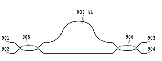
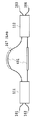
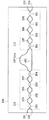
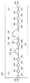
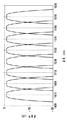
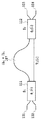
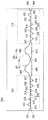
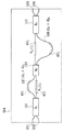
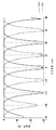
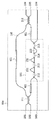
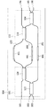
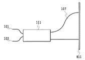
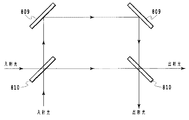
具体例として、図1に従来のマッハツェンダ干渉計を示す。このマッハツェンダ干渉計(例えば、非特許文献7を参照)は、2個の光結合器905,906と、これら2個の光結合器に挟まれた光路長差付与手段907と、光結合器905,906に接続するそれぞれ二本の入出力光導波路より構成されている。なお、光結合器905,906は方向性結合器を用いており、結合率は50%に設定してある。
As a specific example, FIG. 1 shows a conventional Mach-Zehnder interferometer. The Mach-Zehnder interferometer (see, for example, Non-Patent Document 7) includes two
マッハツェンダ干渉計は次に説明するように等周波数間隔の合分波回路である。マッハツェンダ干渉計の二つの光出力強度はそれぞれ、 The Mach-Zehnder interferometer is a multiplexing / demultiplexing circuit with equal frequency intervals as described below. The two light output intensities of the Mach-Zehnder interferometer are
![]()
![]()
![]()
![]()
但し、A0は一方の入力ポートより入射された光強度、ξは光路長差付与手段の位相である。 Where A 0 is the intensity of light incident from one input port, and ξ is the phase of the optical path length difference providing means.
ここで、f=c/λの関係よりξは、 Here, from the relationship f = c / λ, ξ is
![]()
![]()
但し、nは屈折率、ΔLは光路長差、fは周波数、cは光速度、λは波長、mは整数である。 Where n is the refractive index, ΔL is the optical path length difference, f is the frequency, c is the speed of light, λ is the wavelength, and m is an integer.
周波数間隔は、コサイン関数、サイン関数の二乗が周期πの関数であることを用いると、(3)式より Using the cosine function and the square of the sine function as a function of period π, the frequency interval
![]()
![]()
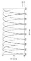
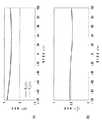
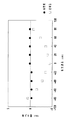
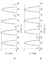
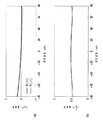
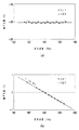
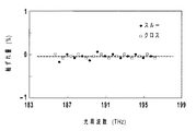
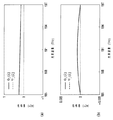
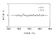
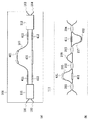
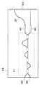
図2に、マッハツェンダ干渉計の中心波長を1470nmとし、その近傍におけるスルーポートとクロスポートの分波間隔が20nmとなるような周波数間隔を与える光路長差、即ち、光路長差付与手段における光学的光路長差を55.9μmに設定した場合の透過特性を示す。ここで、横軸は波長であり、波長グリッドが等間隔に並んでいる。実線はクロスポートより出力される透過特性、破線はスルーポートより出力される透過特性である。 FIG. 2 shows an optical path length difference that gives a frequency interval such that the center wavelength of the Mach-Zehnder interferometer is 1470 nm and the demultiplexing interval between the through port and the cross port in the vicinity is 20 nm, that is, the optical path length difference providing means. The transmission characteristics when the optical path length difference is set to 55.9 μm are shown. Here, the horizontal axis is the wavelength, and wavelength grids are arranged at equal intervals. The solid line is the transmission characteristic output from the cross port, and the broken line is the transmission characteristic output from the through port.
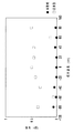
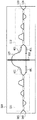
比較のために、横軸を光周波数にした場合の透過特性を図3に示した。マッハツェンダ干渉計の透過特性は、図3に示すように等周波数間隔であり波長間隔は等しくない。1470nm近傍ではスルーポートとクロスポートの分波間隔が20nmであり、波長グリッド上に載っているが、1470nmから長波長側にいくほど波長間隔が広くなり、波長グリッドから離れる様子が明らかである。従って、このような光デバイスは波長グリッド上で挿入損失、透過帯域幅や消光比が波長によって著しく異なり、CWDMシステム用の光デバイスとして使用するには適していなかった。 For comparison, the transmission characteristics when the horizontal axis is the optical frequency are shown in FIG. The transmission characteristics of the Mach-Zehnder interferometer are equal frequency intervals as shown in FIG. 3, and the wavelength intervals are not equal. In the vicinity of 1470 nm, the demultiplexing interval between the through port and the cross port is 20 nm and is placed on the wavelength grid, but it is clear that the wavelength interval increases as the wavelength increases from 1470 nm to the longer wavelength side, and the distance from the wavelength grid increases. Therefore, such an optical device is not suitable for use as an optical device for a CWDM system because its insertion loss, transmission bandwidth, and extinction ratio vary significantly depending on the wavelength on the wavelength grid.
すなわち、従来構成のマッハツェンダ干渉回路等の干渉回路は等波長間隔になっていないため、透過帯は中心波長から離れるほど波長軸上のグリッドからずれ、挿入損失が波長によって著しく異なってしまうという問題があった。 That is, since the interference circuit such as the Mach-Zehnder interference circuit of the conventional configuration is not at the same wavelength interval, the transmission band shifts from the grid on the wavelength axis as the distance from the center wavelength increases, and the insertion loss varies significantly depending on the wavelength. there were.
従来型の光合分波回路は、光周波数領域で等周期な特性を有するが、その透過特性は光周波数間隔と中心光周波数で特徴付けることができる。しかし、従来型光合分波回路で光周波数間隔と中心光周波数に関連し、自由に設定できる設計パラメータは光路長差付与手段の光学的光路長差のみであった。設定が必要なパラメータが2つある一方で、自由に設定可能なパラメータが1つのみであるために、光周波数間隔と中心光周波数とを同時に設定することができなかった。 The conventional optical multiplexing / demultiplexing circuit has an equal period characteristic in the optical frequency region, but its transmission characteristic can be characterized by the optical frequency interval and the central optical frequency. However, in the conventional optical multiplexing / demultiplexing circuit, the design parameter that can be freely set related to the optical frequency interval and the center optical frequency is only the optical optical path length difference of the optical path length difference providing means. While there are two parameters that need to be set, since only one parameter can be freely set, the optical frequency interval and the center optical frequency cannot be set simultaneously.
従って、原理的に等周波数間隔である光合分波回路も、光周波数間隔もしくは中心光周波数の何れかが設定できず、光周波数領域で使用する場合にも、結果的に、透過特性が劣化するという問題があった。 Therefore, in principle, the optical multiplexing / demultiplexing circuit having the equal frequency interval cannot be set either in the optical frequency interval or the central optical frequency, and when used in the optical frequency region, the transmission characteristics are deteriorated as a result. There was a problem.
発明者らは、上述の問題を解決するためには、透過帯が等波長間隔のグリッド上に乗るように、グリッドごとに光路長差ΔLが変化するような仕組みを与え、中心波長をグリッドに一致させるようにできれば良いとの着想に至った。そして、光路長差ΔLは通常、光路長差付与手段により与えられるが、干渉計を構成する光合分波手段の出力の位相差によっても光路長差ΔLを与え得ることに注目した。 In order to solve the above-mentioned problems, the inventors provide a mechanism in which the optical path length difference ΔL changes for each grid so that the transmission band is on the grid with the equal wavelength interval, and the center wavelength is set to the grid. I came up with the idea that it would be better to match. The optical path length difference ΔL is usually given by the optical path length difference providing means, but it has been noted that the optical path length difference ΔL can also be given by the phase difference of the output of the optical multiplexing / demultiplexing means constituting the interferometer.
例えば、マッハツェンダ干渉計の二つの出力ポート間に1周期πの位相差を与えれば、光路長を1/2波長分変化させられる。そこで、出力の位相差が波長依存性を持つような光合分波手段を実現し、マッハツェンダ干渉計の光路長差付与手段に作用させれば、光路長差ΔLを異なる波長ごとに変化させられることになる。 For example, if a phase difference of 1 period π is given between two output ports of a Mach-Zehnder interferometer, the optical path length can be changed by ½ wavelength. Therefore, if an optical multiplexing / demultiplexing means whose output phase difference has wavelength dependence is realized and applied to the optical path length difference providing means of the Mach-Zehnder interferometer, the optical path length difference ΔL can be changed for each different wavelength. become.
しかし、従来技術で用いられている方向性結合器、マルチモード干渉計型カプラなどの従来型の光合分波手段では、その出力の位相差は一定であるため、波長(周波数)に依存する位相差はなく、光路長差ΔLに光合分波手段の寄与による波長(周波数)依存性を与えることができなかった。 However, in conventional optical multiplexing / demultiplexing means such as directional couplers and multimode interferometer type couplers used in the prior art, the phase difference of the output is constant, so that it depends on the wavelength (frequency). There was no phase difference, and wavelength (frequency) dependence due to the contribution of the optical multiplexing / demultiplexing means could not be given to the optical path length difference ΔL.
本発明は、出力の位相差が波長(周波数)依存性を持ち、回路の透過帯域にある波長(周波数)の光に対して異なる位相差を与えるための位相生成機能を備える光合分波手段を実現することにより、透過帯が光周波数グリッドに乗る等光周波数間隔の光合分波回路を提供することを目的とする。 The present invention provides an optical multiplexing / demultiplexing means having a phase generation function for giving a different phase difference to light having a wavelength (frequency) in a transmission band of a circuit, in which an output phase difference has wavelength (frequency) dependence. An object of the present invention is to provide an optical multiplexing / demultiplexing circuit having equal optical frequency intervals in which a transmission band rides on an optical frequency grid.
また、本発明の位相生成手段を用いることにより、光周波数依存性のある位相を光合分波回路に作用させ、光周波数間隔および中心光周波数を何れも任意の値に設定することができる光合分波回路を提供することを目的とする。 Further, by using the phase generation means of the present invention, an optical frequency division that allows an optical frequency dependent phase to act on the optical multiplexing / demultiplexing circuit, and the optical frequency interval and the central optical frequency can be set to arbitrary values. An object is to provide a wave circuit.
上述の目的を達成するために、本発明は、複数の透過帯域から構成される全帯域において複数の光を合波分波する光合分波回路において、入力部と出力部とを有する少なくとも2つの光合分波手段と、前記少なくとも2つの光合分波手段の間に接続された光路長差付与手段とを備え、前記光合分波手段の少なくとも1つは位相生成手段として機能し、前記位相生成手段は、前記出力部の中の2つの出力端から出力される2つの光の位相差として定義される光周波数依存性を持つ位相φを生成し、1つ以上の前記位相生成手段により生成された光周波数の関数によって表され、前記光路長差付与手段に生じさせる光周波数依存性を持つ位相Φが、隣接する前記透過帯域の各中心光周波数の一定の周波数間隔および前記全帯域の中心光周波数を所望の値に同時に設定することを特徴とする光合分波回路である。 In order to achieve the above-described object, the present invention provides an optical multiplexing / demultiplexing circuit that multiplexes / demultiplexes a plurality of lights in an entire band composed of a plurality of transmission bands, and has at least two inputs and outputs. An optical multiplexing / demultiplexing unit; and an optical path length difference providing unit connected between the at least two optical multiplexing / demultiplexing units, wherein at least one of the optical multiplexing / demultiplexing units functions as a phase generating unit, and the phase generating unit Generates a phase φ having an optical frequency dependency defined as a phase difference between two lights output from two output terminals in the output unit, and is generated by one or more of the phase generation means A phase Φ represented by a function of optical frequency and having optical frequency dependency generated in the optical path length difference providing means is a constant frequency interval of each central optical frequency of the adjacent transmission band and a central optical frequency of the entire band. Desired An optical multiplexing and demultiplexing circuit and setting the same time value.
好ましくは、前記全帯域における透過特性が、Nを光合分波回路の次数、xqを展開係数、fを光周波数、Ψ(f)を光周波数領域グリッド上において隣合う透過帯域間の中心光周波数間隔を設定するために必要な光周波数依存性を持つ目標位相、ΔL´(=ΔL+δL)を屈折率の波長依存性を含めた前記光路長差付与手段の光学的光路長差、ΔLを光学的光路長差、δLを微小光学的光路長差とすると、次式により表される。 Preferably, the transmission characteristics in the entire band are such that N is the order of the optical multiplexing / demultiplexing circuit, xq is the expansion coefficient, f is the optical frequency , and Ψ (f) is the center optical frequency between adjacent transmission bands on the optical frequency domain grid. The target phase having optical frequency dependency necessary for setting the interval, ΔL ′ (= ΔL + δL), the optical path length difference of the optical path length difference adding means including the wavelength dependency of the refractive index, and ΔL are optical When the optical path length difference, δL, is defined as a micro optical optical path length difference, it is expressed by the following equation.

さらに好ましくは、光周波数依存性を持つ前記位相Φは、前記光合分波回路の前記全帯域における光周波数(f)の関数によって与えられ、前記関数は2次関数以上の多項式であって、光周波数依存性を持つ前記目標位相Ψは、Δfを光周波数領域グリッド上における合分波回路の光周波数間隔、fcを光合分波回路の全帯域の中心近傍に位置する透過帯域の中心光周波数、mを整数とすると、次式で表わすことができる。 More preferably, the phase Φ having optical frequency dependency is given by a function of the optical frequency (f) in the entire band of the optical multiplexing / demultiplexing circuit, and the function is a polynomial having a quadratic function or more, The target phase Ψ having frequency dependence is expressed as follows: Δf is the optical frequency interval of the multiplexing / demultiplexing circuit on the optical frequency domain grid, fc is the center optical frequency of the transmission band located near the center of the entire band of the optical multiplexing / demultiplexing circuit, If m is an integer, it can be expressed by the following equation.
隣合う前記光結合器の間に配置されたM個の光路長差付与部とから構成されており、前記光周波数依存性を持つ位相を、前記光結合器の振幅結合率および前記光路長差付与部の光学的光路長差をそれぞれ最適化することによって生成することもできる。
Said optical coupler M optical path length difference imparting portion disposed between the adjacent and are composed of a phase having the optical frequency dependent amplitude coupling rate and the optical path length of said optical coupler It can also be generated by optimizing the optical path length difference of the difference providing unit.
また、前記位相生成手段は、(M+1)個(Mは2以上の整数)の光結合器と、隣合う前記光結合器の間に配置されたM個の光路長差付与部とから構成されており、光周波数依存性を持つ前記位相Φが光周波数依存性を持つ前記目標位相Ψに等しく成るように、前記光結合器の振幅結合率および前記光路長差付与部の光学的光路長差ならびに前記光合分波回路が備える前記光路長差付与手段に付加する光学的光路長差δLの各々が設定されても良い。 In addition, the phase generation unit includes (M + 1) (M is an integer of 2 or more) optical couplers and M optical path length difference providing units arranged between the adjacent optical couplers. and which, as the phase Φ with the optical frequency dependence is made equal to the target phase having an optical frequency dependence [psi, optical Tekihikariro amplitude coupling rate and the optical path length difference imparting portion of the optical coupler Each of the length difference and the optical path length difference ΔL added to the optical path length difference providing means provided in the optical multiplexing / demultiplexing circuit may be set.
また、前記光合分波回路は光干渉回路であり、前記光干渉回路は、(N+1)個(Nは1以上の整数)の前記光合分波手段と、隣合う前記光合分波手段の間に配置されたN個の前記光路長差付与手段とを接続して構成することができる。 The optical multiplexing / demultiplexing circuit is an optical interference circuit, and the optical interference circuit is provided between (N + 1) (N is an integer of 1 or more) optical multiplexing / demultiplexing means and the adjacent optical multiplexing / demultiplexing means. It can be configured by connecting the N optical path length difference providing means arranged.
本発明の別の態様では、前記光合分波回路は、2つの前記光合分波手段と、前記2つの光合分波手段の間に配置された前記光路長差付与手段と、前記光合分波手段の一方に接続された少なくとも1本の入力導波路および前記光合分波手段の他方に接続された複数本の出力導波路と、を備えたマッハツェンダ干渉回路であり、前記2つの光合分波手段は、前記マッハツェンダ干渉回路の中間点に対して左右対称に配置されており、前記2つの光合分波手段のいずれもが位相生成手段を備えた位相生成光結合器であり、前記位相生成光結合器は、4つの光結合器と、隣合う前記光結合器の間にそれぞれ配置された3つの光路長差付与部と、によって構成されていても良い。 In another aspect of the present invention, the optical multiplexing / demultiplexing circuit includes two optical multiplexing / demultiplexing units, the optical path length difference providing unit disposed between the two optical multiplexing / demultiplexing units, and the optical multiplexing / demultiplexing unit. A Mach-Zehnder interference circuit comprising at least one input waveguide connected to one of the optical waveguides and a plurality of output waveguides connected to the other of the optical multiplexing / demultiplexing means, wherein the two optical multiplexing / demultiplexing means The phase generation optical coupler is a phase generation optical coupler which is arranged symmetrically with respect to the intermediate point of the Mach-Zehnder interference circuit, and both of the two optical multiplexing / demultiplexing means include phase generation means. May be configured by four optical couplers and three optical path length difference providing units respectively disposed between the adjacent optical couplers.
さらに好ましくは、前記光合分波回路は、2つの前記光合分波手段と、前記2つの光合分波手段の間に配置された前記光路長差付与手段と、前記光合分波手段の一方に接続された少なくとも1本の入力導波路および前記光合分波手段の他方に接続された複数本の出力導波路と、を備えたマッハツェンダ干渉回路であり、前記2つの光合分波手段のいずれか一方は、位相生成手段を備えた位相生成光結合器であり、前記位相生成光結合器は、(M+1)個(Mは2以上の整数)の光結合器と、隣合う前記光結合器の間に配置されたM個の光路長差付与部と、によって構成されていても良い。 More preferably, the optical multiplexing / demultiplexing circuit is connected to one of the two optical multiplexing / demultiplexing means, the optical path length difference providing means disposed between the two optical multiplexing / demultiplexing means, and the optical multiplexing / demultiplexing means. A Mach-Zehnder interference circuit comprising at least one input waveguide and a plurality of output waveguides connected to the other of the optical multiplexing / demultiplexing means, wherein one of the two optical multiplexing / demultiplexing means is , A phase generation optical coupler including phase generation means, wherein the phase generation optical coupler is provided between (M + 1) (M is an integer of 2 or more) optical couplers and the adjacent optical couplers. You may be comprised by the M optical path length difference provision part arrange | positioned.
また、前記光合分波回路は、第1乃至第3の3つの前記光合分波手段と、隣合う前記3つの光合分波手段の間にそれぞれ配置された2つの前記光路長差付与手段と、前記第1の光合分波手段に接続された少なくとも1本の入力導波路と、前記第3の光合分波手段に接続された少なくとも1本の出力導波路とを備えたラティス・フィルタであり、前記第1および第3の光合分波手段は位相生成手段を備えた位相生成光結合器であり、前記位相生成光結合器は、(M+1)個(Mは2以上の整数)の光結合器と、隣合う前記光結合器の間にそれぞれ配置されたM個の光路長差付与部と、によって構成することもできる。 The optical multiplexing / demultiplexing circuit includes first to third optical multiplexing / demultiplexing units and two optical path length difference providing units arranged between the adjacent three optical multiplexing / demultiplexing units, A lattice filter comprising at least one input waveguide connected to the first optical multiplexing / demultiplexing means and at least one output waveguide connected to the third optical multiplexing / demultiplexing means; The first and third optical multiplexing / demultiplexing means are phase generating optical couplers having phase generating means, and the number of phase generating optical couplers is (M + 1) (M is an integer of 2 or more) optical couplers. And M optical path length difference providing units respectively disposed between the adjacent optical couplers.
好ましくは、上述の各光合分波回路は、トランスバーサル・フィルタとすることもできる。 Preferably, each of the optical multiplexing / demultiplexing circuits described above can be a transversal filter.
本発明のさらに別の態様においては、アレイ導波路回折格子と、前記アレイ導波路回折格子の一端に接続された第1のスラブ導波路と、前記アレイ導波路回折格子の他端に接続された第2のスラブ導波路と、前記第2のスラブ導波路に接続された出力導波路とを備え、上述の光合分波回路の出力が前記第1のスラブ導波路に光学的に接続されていても良い。 In yet another aspect of the present invention, the arrayed waveguide diffraction grating, the first slab waveguide connected to one end of the arrayed waveguide diffraction grating, and the other end of the arrayed waveguide diffraction grating are connected. A second slab waveguide; and an output waveguide connected to the second slab waveguide, wherein an output of the optical multiplexing / demultiplexing circuit is optically connected to the first slab waveguide. Also good.
同様に、アレイ導波路回折格子と、前記アレイ導波路回折格子の一端に接続された第1のスラブ導波路と、前記第1のスラブ導波路に接続された入力導波路と、前記アレイ導波路回折格子の他端に接続された第2のスラブ導波路とを備え、前記第2のスラブ導波路の出力が上述の光合分波回路に光学的に接続されていても良い。 Similarly, an arrayed waveguide diffraction grating, a first slab waveguide connected to one end of the arrayed waveguide grating, an input waveguide connected to the first slab waveguide, and the arrayed waveguide A second slab waveguide connected to the other end of the diffraction grating, and an output of the second slab waveguide may be optically connected to the optical multiplexing / demultiplexing circuit.
さらに好ましくは、前記光合分波回路は2つの前記光合分波手段を備え、前記光路長差付与手段は隣合う前記光合分波手段の間に配置された2本の光遅延線により構成されており、前記2つの光合分波手段の一方に少なくとも1本の入力導波路が接続され、前記2つの光合分波手段の他方が前記アレイ導波路回折格子の第1のスラブ導波路もしくは第2のスラブ導波路の少なくとも一方に接続されていても良い。 More preferably, the optical multiplexing / demultiplexing circuit includes two optical multiplexing / demultiplexing units, and the optical path length difference providing unit includes two optical delay lines disposed between the adjacent optical multiplexing / demultiplexing units. And at least one input waveguide is connected to one of the two optical multiplexing / demultiplexing means, and the other of the two optical multiplexing / demultiplexing means is connected to the first slab waveguide or the second of the arrayed waveguide diffraction grating. It may be connected to at least one of the slab waveguides.
さらに、上述のいずれかに記載の光合分波回路の少なくとも一方の出力側に、上述のいずれかに記載の光合分波回路が1つ以上接続されていても良い。 Furthermore, one or more optical multiplexing / demultiplexing circuits described above may be connected to at least one output side of the optical multiplexing / demultiplexing circuit described above.
本発明の他の実施態様の光合分波回路は、複数の透過帯域から構成される全帯域において複数の光を合波分波する光合分波回路において、入力部と出力部とを有する少なくとも1つの光合分波手段と、前記少なくとも1つの光合分波手段の前記出力部に光学的に接続された光路長差付与手段と、前記光路長差付与手段に接続された反射板とを備え、前記反射板を信号光の折り返し点とする反射型の光合分波回路であって、前記光合分波手段の少なくとも1つは位相生成手段として機能し、前記位相生成手段は、前記出力部の中の2つの出力端から出力される2つの光の位相差として定義される光周波数依存性を持つ位相φを生成し、1つ以上の前記位相生成手段により生成された光周波数の関数によって表され、前記光路長差付与手段に生じさせる光周波数依存性を持つ位相Φが、隣接する前記透過帯域の各中心光周波数の一定間隔および前記全帯域の中心光周波数を所望の値に同時に設定することを特徴とする。 An optical multiplexing / demultiplexing circuit according to another embodiment of the present invention is an optical multiplexing / demultiplexing circuit that multiplexes / demultiplexes a plurality of lights in an entire band composed of a plurality of transmission bands, and has at least one input unit and an output unit. Two optical multiplexing / demultiplexing means, an optical path length difference providing means optically connected to the output part of the at least one optical multiplexing / demultiplexing means, and a reflector connected to the optical path length difference providing means, A reflection type optical multiplexing / demultiplexing circuit having a reflecting plate as a turning point of signal light, wherein at least one of the optical multiplexing / demultiplexing means functions as a phase generating means, and the phase generating means is provided in the output unit. A phase φ having an optical frequency dependency defined as a phase difference between two lights output from the two output ends, and expressed by a function of the optical frequency generated by one or more of the phase generating means; Occurs in the optical path length difference providing means Phase Φ is having an optical frequency dependence to, and sets the predetermined interval and the center optical frequency of the full bandwidth of the center optical frequency of the transmission band adjacent to the same time a desired value.
好ましくは、前記位相生成手段は、(M+1)個(Mは2以上の整数)の光結合器と、隣合う前記光結合器の間に配置されたM個の光路長差付与部とから構成されており、前記光周波数依存性を持つ位相は、前記光結合器の振幅結合率および前記光路長差付与部の光学的光路長差をそれぞれ最適化することによって生成されるのが良い。 Preferably, the phase generation means includes (M + 1) (M is an integer of 2 or more) optical couplers and M optical path length difference providing units arranged between the adjacent optical couplers. The phase having the optical frequency dependency may be generated by optimizing the amplitude coupling ratio of the optical coupler and the optical optical path length difference of the optical path length difference providing unit.
上述の各光合分波隘路において、前記光路長差付与部には、位相調整手段が備えられているか、または、位相調整がなされていることが好ましい。 In each of the above-described optical multiplexing / demultiplexing bottlenecks, it is preferable that the optical path length difference providing unit is provided with phase adjusting means or phase adjusted.
さらに上述の各光合分波隘路において、前記光路長差付与部には、複屈折調整手段が備えられているか、または、複屈折調整がなされていることが好ましい。 Further, in each of the optical multiplexing / demultiplexing bottleneck described above, it is preferable that the optical path length difference providing unit is provided with birefringence adjusting means or birefringence adjustment is performed.
さらに上述の各光合分波隘路において、前記光合分波回路は、石英系ガラス光導波路で構成されていても良い。 Furthermore, in each of the above-described optical multiplexing / demultiplexing bottles, the optical multiplexing / demultiplexing circuit may be formed of a silica glass optical waveguide.
また、さらに上述のいずれかに記載の光合分波回路が筐体の内部に格納され、前記筐体に保持された光ファイバにより前記光合分波回路への光の入出力を行うことが好ましい。 Furthermore, it is preferable that the optical multiplexing / demultiplexing circuit according to any one of the above is housed in a casing, and light is input / output to / from the optical multiplexing / demultiplexing circuit by an optical fiber held in the casing.
本発明のさらに他の実施態様は、複数の透過帯域から構成される全帯域において複数の光を合波分波する光合分波回路の設計方法であって、前記光合分波回路は、入力部と出力部とを有する少なくとも2つの光合分波手段と、前記少なくとも2つの光合分波手段の間に接続された光路長差付与手段とを備え、前記光合分波手段の少なくとも1つは位相生成手段として機能し、前記位相生成手段は、前記出力部の中の2つの出力端から出力される2つの光の位相差として定義される光周波数依存性を持つ位相φを生成し、前記方法は、光周波数依存性を持つ目標位相Ψを決定するステップであって、前記目標位相Ψは、隣接する前記透過帯域の各中心光周波数の一定の光周波数間隔および前記全帯域の中心光周波数を所望の値に同時に設定するのに必要な位相であるステップと、1つ以上の前記位相生成手段により生成された光周波数の関数によって表され、前記光路長差付与手段に生じさせる光周波数依存性を持つ位相Φが、光周波数依存性を持つ前記目標位相Ψ(f)に等しくなるように前記位相生成手段を構成するステップとを備えることを特徴とする設計方法とすることができる。 Still another embodiment of the present invention is a method of designing an optical multiplexing / demultiplexing circuit for multiplexing / demultiplexing a plurality of lights in an entire band composed of a plurality of transmission bands, wherein the optical multiplexing / demultiplexing circuit includes an input unit And at least two optical multiplexing / demultiplexing means, and an optical path length difference providing means connected between the at least two optical multiplexing / demultiplexing means, wherein at least one of the optical multiplexing / demultiplexing means generates a phase The phase generation means generates a phase φ having an optical frequency dependency defined as a phase difference between two lights output from two output terminals in the output unit, and the method includes: Determining a target phase Ψ having an optical frequency dependency, wherein the target phase Ψ is a desired optical frequency interval of each central optical frequency of the adjacent transmission band and a central optical frequency of the entire band. value be set to the same time of A step which is required phase is represented by one or more of the phase function of the optical frequency generated by the generation means, phase Φ with an optical frequency dependence that causes the optical path length difference imparting means, an optical frequency dependent And a step of configuring the phase generation means so as to be equal to the target phase ψ (f) having a characteristic.
好ましくは、光周波数依存性を持つ目標位相Ψを決定する前記ステップは、前記全帯域における透過特性が、Nを光合分波回路の次数、xqを展開係数、fを光周波数、Ψ(f)を光周波数領域グリッド上において隣合う透過帯域間の中心光周波数間隔を設定するために必要な光周波数依存性を持つ目標位相、ΔL´(=ΔL+δL)を屈折率の波長依存性を含めた前記光路長差付与手段の光学的光路長差、ΔLを光学的光路長差、δLを微小光学的光路長差とすると、次式によって表されるように、光周波数依存性を持つ前記目標位相Ψ(f)を決定するステップを含むことを特徴とする。 Preferably, in the step of determining the target phase Ψ having optical frequency dependency, the transmission characteristics in the entire band are such that N is the order of the optical multiplexing / demultiplexing circuit, xq is the expansion coefficient, f is the optical frequency, Ψ (f) Is a target phase having an optical frequency dependency necessary for setting a center optical frequency interval between adjacent transmission bands on the optical frequency domain grid, and ΔL ′ (= ΔL + δL) including the wavelength dependency of the refractive index. Assuming that the optical path length difference of the optical path length difference providing means, ΔL is the optical path length difference, and δL is the micro optical path length difference, the target phase Ψ having optical frequency dependence as expressed by the following equation: The step of determining (f) is included.
また、光周波数依存性を持つ目標位相Ψを決定する前記ステップは、光合分波回路を作成して、全通信帯域に渡って透過特性を測定するステップと、光周波数領域グリッド上において、前記測定された各々の透過帯域の中心光周波数と所望の光周波数とのずれ量に基づいて、前記目標位相Ψを決定するステップとを含むこともできる。 Further, the step of determining the target phase Ψ having optical frequency dependency includes the step of creating an optical multiplexing / demultiplexing circuit and measuring the transmission characteristics over the entire communication band, and the measurement on the optical frequency domain grid. Determining the target phase Ψ based on the amount of deviation between the center optical frequency of each transmission band and the desired optical frequency.
本発明の位相生成機能を備えた光合分波器を用いることにより、光周波数依存性のある位相を光合分波回路に作用させ、光周波数間隔および中心光周波数を何れも任意の値に設定可能な光合分波回路を提供することができる。 By using an optical multiplexer / demultiplexer equipped with the phase generation function of the present invention, an optical frequency dependent phase can be applied to the optical multiplexing / demultiplexing circuit, and the optical frequency interval and the center optical frequency can be set to arbitrary values. An optical multiplexing / demultiplexing circuit can be provided.
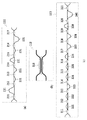
以下、図面を参照して参考例とともに本発明の実施の形態を詳細に説明する。なお、以下では、「光合分波手段」とは、光結合器と光路長差付与部で構成される回路、「位相生成手段」とは、位相Φを生成する手段、「位相生成光結合器」とは、位相生成手段および光合分波手段として機能する回路、を意味する。 Hereinafter, embodiments of the present invention will be described in detail with reference examples with reference to the drawings. In the following, “optical multiplexing / demultiplexing means” means a circuit composed of an optical coupler and an optical path length difference providing unit, and “phase generation means” means means for generating a phase Φ, “phase generation optical coupler” "Means a circuit that functions as a phase generation means and an optical multiplexing / demultiplexing means.
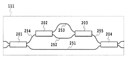
(参考例の第1の実施形態)
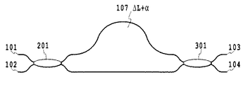
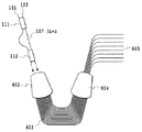
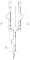
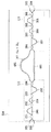
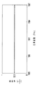
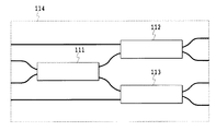
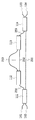
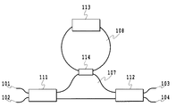
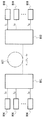
本発明の第1の実施形態における光合分波回路を図4に示す。本回路は、2入力2出力の2個の位相生成光結合器111,112と、これら2個の位相生成光結合器111,112に挟まれた2本の光導波路からなる光路長差付与手段107と、位相生成光結合器111,112に接続するそれぞれ二本の入出力光導波路101,102及び103,104より構成されている。
(First embodiment of reference example )
FIG. 4 shows an optical multiplexing / demultiplexing circuit according to the first embodiment of the present invention. This circuit includes two phase generation
この光合分波回路は、その透過特性が波長軸上において概ね等周期となるように、波長間隔のずれを補正する機能(位相生成機能)を備えている。この機能は、例えば、位相生成光結合器111,112の何れかまたは両方を、出力の位相差が光合分波回路の透過帯域にある波長に対して依存性をもつように構成することにより実現できる。また、光路長差付与手段107の光導波路上に、波長依存性をもつ位相差を生成可能な位相生成手段を設けることによっても係る機能を実現することが可能である。
This optical multiplexing / demultiplexing circuit has a function (phase generation function) for correcting the shift of the wavelength interval so that the transmission characteristics thereof have substantially the same period on the wavelength axis. This function is realized, for example, by configuring either or both of the phase generation
以下に、この位相補正について詳しく説明する。
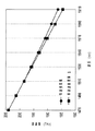
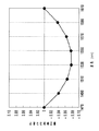
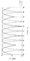
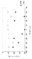
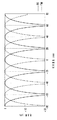
一般的な波長と周波数の関係を図5に示す。CWDMグリッド上の波長に対する周波数を、f=c/λより求め、プロットしたものを「等波長間隔」と示した。但し、fは周波数、cは光速度、λは波長である。また1470nm近傍での周波数間隔Δf1を求め(≒2.74THz)、1470nmにおける周波数を基準に、等しい周波数間隔でCWDMグリッドに対する周波数をプロットしたものを「等周波数間隔1」と示した。
The phase correction will be described in detail below.
FIG. 5 shows a general relationship between wavelength and frequency. The frequency with respect to the wavelength on the CWDM grid was obtained from f = c / λ, and the plotted frequency was shown as “equal wavelength interval”. Where f is the frequency, c is the speed of light, and λ is the wavelength. A frequency interval Δf 1 in the vicinity of 1470 nm was obtained (≈2.74 THz), and the frequency plotted against the CWDM grid at equal frequency intervals with reference to the frequency at 1470 nm was indicated as “
1470nm近傍では両者は一致しているが、1470nmから離れるほど両者のずれは大きくなっていく。このことは図2に示した従来のマッハツェンダ干渉計の透過特性の傾向と一致する。即ち、1470nm近傍ではクロスポートの透過率は高く、スルーポートのクロストークは低く抑えられているが、長波長側に離れるほど透過特性はグリッドからずれ、波長軸上における透過率は低くなり、クロストークは劣化する。 In the vicinity of 1470 nm, both coincide with each other, but as the distance from 1470 nm increases, the difference between the two increases. This coincides with the tendency of the transmission characteristics of the conventional Mach-Zehnder interferometer shown in FIG. That is, in the vicinity of 1470 nm, the cross-port transmittance is high and the cross-talk of the through port is kept low. However, as the distance from the long wavelength side increases, the transmission characteristics deviate from the grid, and the transmittance on the wavelength axis decreases. Talk deteriorates.
そこで、図5の等波長間隔と等周波数間隔1のずれを補正するため、このずれを線形部分と非線形部分に分け、次のように補正した。まず、等波長間隔と等周波数間隔1のずれの線形部分の補正法について説明する。
Therefore, in order to correct the shift between the equal wavelength interval and the
1470nm近傍における周波数間隔と1610nm近傍における周波数間隔の平均値から周波数間隔Δf2を求め(≒2.53THz)、図6に示すように、1470nmにおける周波数を基準に、等しい周波数間隔でCWDMグリッド上の波長に対する周波数をプロットしたものを「等周波数間隔2」と示した。
A frequency interval Δf 2 is obtained from an average value of the frequency interval in the vicinity of 1470 nm and the frequency interval in the vicinity of 1610 nm (≈2.53 THz). As shown in FIG. 6, the frequency interval on the CWDM grid is equal to the frequency at 1470 nm. A plot of frequency versus wavelength is shown as “
1470nm付近では等波長間隔と等周波数間隔2とは一致し、長波長側に移るにつれ若干ずれが生じ、1610nm付近では再び両者は一致した。このような線形部分の補正により、等波長間隔と等周波数間隔とのずれはほとんど補正できることがわかる。
In the vicinity of 1470 nm, the equal wavelength interval and the
等波長間隔と等周波数間隔のずれの線形部分を補正したマッハツェンダ干渉計を図7に示す。この回路は、2個の光結合器201,301と、これら2個の光結合器201,301に挟まれた光路長差付与手段107と、光結合器201,301に接続するそれぞれ二本の入出力光導波路101,102及び103,104を有する。なお、光結合器201,301は方向性結合器を用いており、結合率は50%に設定してある。
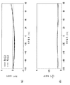
FIG. 7 shows a Mach-Zehnder interferometer in which the linear portion of the shift between the equal wavelength interval and the equal frequency interval is corrected. This circuit includes two
従来のマッハツェンダ干渉計の光路長差付与手段における光路長差はΔLであるのに対し、本回路の光路長差はΔL’=ΔL+αに設定されている。但し、ΔL=55.9μm、αは波長オーダーの光路長であり、α=2・λc(λcは中心波長であり、例えばλc=1.47μmならα=2.94μmである)に設定した。 The optical path length difference in the optical path length difference providing means of the conventional Mach-Zehnder interferometer is ΔL, whereas the optical path length difference of this circuit is set to ΔL ′ = ΔL + α. However, ΔL = 55.9 μm, α is the optical path length on the order of wavelength, and α = 2 · λ c (λ c is the central wavelength; for example, when λ c = 1.47 μm, α = 2.94 μm). Set.
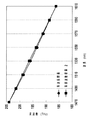
この時の透過特性の波長依存性を図8に示す。図6に示した等波長間隔と等周波数間隔2のずれの傾向と同様に、波長軸上の真中では若干ずれているが、両端ではちょうどグリッド上に乗っている。そのため、波長領域の両端では波長軸上における透過率は高く、クロストークは低く抑えられており、特性は改善されている。
The wavelength dependence of the transmission characteristics at this time is shown in FIG. Similar to the tendency of the shift between the equal wavelength interval and the
このように、等波長間隔と等周波数間隔のずれの線形部分は、光路長差付与手段に波長オーダーの補正を与えることにより補正できる。しかし、依然として、波長軸上の中心部分には若干のずれがある。そこで、この等波長間隔と等周波数間隔のずれの非線形部分を位相生成光結合器により補正する方法を次に説明する。 As described above, the linear portion of the shift between the equal wavelength interval and the equal frequency interval can be corrected by correcting the wavelength order to the optical path length difference providing unit. However, there is still a slight shift in the central portion on the wavelength axis. Therefore, a method for correcting the nonlinear portion of the deviation between the equal wavelength interval and the equal frequency interval by the phase generation optical coupler will be described below.
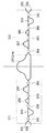
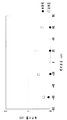
CWDMグリッド上の各波長に対し、図6で示した等波長間隔と等周波数間隔2の周波数ずれを周波数間隔Δf2で割った値、即ち等波長間隔と等周波数間隔のずれの非線形部分の補正に必要な位相補正量をプロットした結果を図9に示した。すなわち、図9に示した位相補正量を各波長の光に対して与えることとすれば、等波長間隔と等周波数間隔2のずれの非線形部分を補正することができることとなる。
For each wavelength on the CWDM grid, a value obtained by dividing the frequency shift between the equal wavelength interval and the
先ず、図9に示した出力位相差の波長依存性を関数的に表現する例について説明する。 波長と周波数の関係式f=c/λにおいて、m番目の波長λmとm番目の周波数fm=f0+mΔfとの関係は、 First, an example in which the wavelength dependence of the output phase difference shown in FIG. 9 is expressed functionally will be described. In the relational expression f = c / λ between the wavelength and the frequency, the relationship between the mth wavelength λ m and the mth frequency f m = f 0 + mΔf is
![]()
![]()
例えば、二次の多項式による近似を行う場合、多重回帰近似を行った結果、図9の曲線は、位相補正量Ψが For example, in the case of approximation by a quadratic polynomial, as a result of performing multiple regression approximation, the curve in FIG.
![]()
![]()
と近似できた。 I was able to approximate.
もちろん、二次関数以上の多項式には限定されず、任意の関数を用いて近似しても良い。例えば、ガウス関数を用いて近似する場合は、近似式は、位相補正量Ψが Of course, the polynomial is not limited to a quadratic function or higher, and approximation may be performed using an arbitrary function. For example, when approximating using a Gaussian function, the approximate expression is that the phase correction amount Ψ is
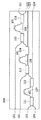
このような位相差の波長依存性を与える手段として、干渉回路の透過帯域の波長(本実施形態の場合1470〜1610nm)に対して互いに異なる出力位相差をもつ位相生成光結合器を用いることにした。出力の位相差の波長依存性が合分波回路の透過帯域に対して変化する位相生成光結合器の構成例を図10に示す。 As means for providing such wavelength dependence of the phase difference, a phase generation optical coupler having different output phase differences with respect to the wavelength of the transmission band of the interference circuit (1470 to 1610 nm in this embodiment) is used. did. FIG. 10 shows a configuration example of a phase generation optical coupler in which the wavelength dependence of the output phase difference changes with respect to the transmission band of the multiplexing / demultiplexing circuit.
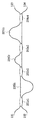
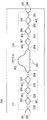
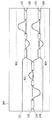
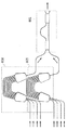
この位相生成光結合器は、4つの光結合器201〜204と、隣接する光結合器201〜204に挟まれた3つの光路長差付与部分205〜207より構成されている。4つの光結合器201〜204の結合率を適切な値に設定し、3つの光路長差付与部205〜207に適切な光路長差を与えることにより、この位相生成光結合器の結合率の値と、出力の位相差の波長依存性を任意に設定することができる。
This phase generation optical coupler is composed of four
光結合器201,202,203,204には、結合率がそれぞれr1,r2,r3,r4の方向性結合器を用いることとした。また、光路長差付与部205,206,207の光路長差はそれぞれδ1、δ2、δ3とした。位相生成光結合器の出力の位相特性を上記(7)式の近似関数にフィッティングした結果、結合率r1=82%、r2=82%、r3=82%、r4=82%、光路長差δ1=−1.13λc、δ2=0.24λc、δ3=1.13λcが得られた。
As the
ここでは、光路長差付与部が3つ(光結合器が4つ)の位相生成光結合器を用いることとしているが、光路長差付与部は2つでも良いし、4つでも良い。なお、光路長差付与部の数が多いほど位相生成光結合器の位相特性を制御する自由度が高まり、フィッティングの精度は高まる。しかし、光路長差付与部の数が増えるほど回路サイズも大きくなるため、充分な近似度が得られる最小限の光長差付与部数で位相生成光結合器を構成することが望ましい。具体的には、光路長差付与部の数が6つ(光結合器が7つ)を超えると回路サイズが大きくなってしまうため、光路長差付与部の数は6つ以下に設定するのが望ましい。 Here, a phase generation optical coupler having three optical path length difference providing units (four optical couplers) is used, but the number of optical path length difference providing units may be two or four. Note that the greater the number of optical path length difference providing units, the greater the degree of freedom for controlling the phase characteristics of the phase generating optical coupler, and the fitting accuracy increases. However, since the circuit size increases as the number of optical path length difference providing units increases, it is desirable to configure the phase generation optical coupler with a minimum number of optical length difference providing units that can provide a sufficient degree of approximation. Specifically, if the number of optical path length difference imparting units exceeds six (seven optical couplers), the circuit size increases, so the number of optical path length difference imparting units is set to six or less. Is desirable.
当然のことではあるが、光路長差付与部の大きさは、導波路の比屈折率差、光路長、光結合器の結合率、回路構成などにより変化し、必要な位相補正量は、使用する光結合器の波長依存性、導波路材料の特性、分波間隔、回路構成などにより異なるため、作製する回路に合わせて光路長差付与部の数を設定すれば良い。本実施形態における好適な干渉回路は、図11に示すように、光路長差付与手段107に接続されている光合分波手段111,112の各々が、3つの光路長差付与部(205,206,207および305,306,307)を有するように構成されたものである。
As a matter of course, the size of the optical path length difference providing unit varies depending on the relative refractive index difference of the waveguide, the optical path length, the coupling rate of the optical coupler, the circuit configuration, and the necessary phase correction amount is used. Therefore, the number of optical path length difference imparting portions may be set in accordance with the circuit to be manufactured. As shown in FIG. 11, in the preferred interference circuit in this embodiment, each of the optical multiplexing /
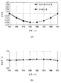
図10に示した構成の位相生成光結合器を、従来構成の非対称マッハツェンダ干渉計が備える二つの光結合器として使用することとした。図12(a)には、この非対称マッハツェンダ干渉計の光結合器(位相生成光結合器)の二つの出力ポートから出力される光信号の位相差の波長依存性が、図12(b)には、光結合率の波長依存性が示してある。ここで、2πの位相差あたりの光路長の変化は1・λcであり、λcは中心波長、光路長差は一方の導波路(図10では下側の光路)に対する他方の導波路の相対的な光路長であらわした。非対称マッハツェンダ干渉計の従来の二つの光結合器を、本実施形態の位相生成光結合器で置き換えることにより、図12(a)に示されているように、一つの位相生成光結合器あたりに必要な位相補正量は図6に示した値の約半分となる。 The phase generation optical coupler having the configuration shown in FIG. 10 is used as two optical couplers included in the conventional asymmetric Mach-Zehnder interferometer. FIG. 12A shows the wavelength dependence of the phase difference of the optical signal output from the two output ports of the optical coupler (phase generation optical coupler) of this asymmetric Mach-Zehnder interferometer. Indicates the wavelength dependence of the optical coupling factor. Here, the change in the optical path length per 2π phase difference is 1 · λ c , where λ c is the center wavelength, and the optical path length difference is that of the other waveguide relative to one waveguide (the lower optical path in FIG. 10). It was expressed as a relative optical path length. By replacing the conventional two optical couplers of the asymmetric Mach-Zehnder interferometer with the phase generation optical coupler of this embodiment, as shown in FIG. The required phase correction amount is about half of the value shown in FIG.
なお、非対称マッハツェンダ干渉計の左右の位相生成光結合器で異なる位相補正量を与えても良いし、片側の位相生成光結合器のみで位相補正を行っても良いことはいうまでもない。例えば、図4において、位相生成光結合器111として出力の位相差が一定である従来の光結合器を用いる一方、位相生成光結合器112として出力の位相差が合分波器の透過帯域の波長に対して変化する位相生成光結合器(例えば、光路長差付与部が6つ(光結合器が7つ)の位相生成光結合器)を用いることとし、この位相生成光結合器112のみで図12(a)に示した位相補正量および図12(b)に示した結合率を実現しても同様の効果が得られる。
Of course, different phase correction amounts may be given by the left and right phase generation optical couplers of the asymmetric Mach-Zehnder interferometer, or the phase correction may be performed by only one phase generation optical coupler. For example, in FIG. 4, a conventional optical coupler having a constant output phase difference is used as the phase generation
すなわち、干渉回路を構成する位相生成光結合器の一つのみを、出力位相差が波長依存性を有するように構成することとしても、等波長間隔回路を実現することができる。 That is, an equal wavelength interval circuit can be realized by configuring only one of the phase generation optical couplers constituting the interference circuit so that the output phase difference has wavelength dependency.
図12(a)に示した位相補正量の波長依存性によれば、図10に示した構成の位相生成光結合器の出力ポートから出力される光信号の互いの位相差には2次関数以上の多項式で与えられる波長依存性があり、等波長間隔と等周波数間隔のずれの非線形部分の補正に必要な位相補正量を示す曲線と一致することがわかる。また、この位相生成光結合器の結合率の波長依存性は小さいため、この位相生成光結合器を用いた合分波回路の透過特性の波長依存性は小さいと予想される。 According to the wavelength dependency of the phase correction amount shown in FIG. 12A, the phase difference between the optical signals output from the output ports of the phase generating optical coupler having the configuration shown in FIG. It can be seen that there is a wavelength dependency given by the above polynomial, and it matches the curve indicating the amount of phase correction required for correcting the non-linear portion of the shift between the equal wavelength interval and the equal frequency interval. Further, since the wavelength dependency of the coupling factor of the phase generation optical coupler is small, it is expected that the wavelength dependency of the transmission characteristics of the multiplexing / demultiplexing circuit using the phase generation optical coupler is small.
図10に示した位相生成光結合器を、図4の合分波回路を構成する二つの位相生成光結合器111,112として用いた場合の透過特性の波長依存性を図13に示した。光路長差付与手段107の光路長差はΔL’=ΔL+αであり、ΔL=55.9μm、α=3.5・λc(λcは中心波長であり例えばλc=1.47μmならα=5.145μmである)に設定した。
FIG. 13 shows the wavelength dependence of the transmission characteristics when the phase generation optical coupler shown in FIG. 10 is used as the two phase generation
また、二つの位相生成光結合器の与える位相差が互いに強め合うようにするため、例えば図11に示したように、光路長差付与手段107の中間点(図の点線)に対し、位相生成光結合器が互いに左右対称になるよう配置した。
Further, in order to intensify the phase difference given by the two phase generation optical couplers, for example, as shown in FIG. 11, the phase generation is performed with respect to the intermediate point (dotted line in the figure) of the optical path length
等波長間隔と等周波数間隔のずれの線形部分は光路長差付与手段で補正されている。さらに、等波長間隔と等周波数間隔のずれの非線形部分は、出力位相差が波長依存性を持つ位相生成光結合器で補正されたことにより、透過特性の波長依存性は全波長範囲でCWDMグリッド上に乗っている。なお、透過特性の波長依存性は小さく、全波長領域にわたってクロストークが良好である。 The linear part of the deviation between the equal wavelength interval and the equal frequency interval is corrected by the optical path length difference providing means. Furthermore, the nonlinear part of the shift between the equal wavelength interval and the equal frequency interval is corrected by the phase generation optical coupler whose output phase difference has the wavelength dependency, so that the wavelength dependency of the transmission characteristic is CWDM grid in the entire wavelength range. It ’s on top. Note that the wavelength dependence of the transmission characteristics is small, and the crosstalk is good over the entire wavelength region.
このような光合分波回路は、火炎堆積法、フォトリソグラフィ、反応性イオンエッチングなどを用いてシリコン基板上に石英系光導波路を形成することにより作製した。なお、導波路の比屈折率差は0.75%、導波路のコア厚は7μm、コア幅は7μmとなるよう製造した。作製した回路は基板から切断した後、ファイバを接続し、モジュール化を行った。本実施形態で用いた導波路材料では、使用する波長帯域における屈折率の波長依存性が小さかったため、屈折率は定数であるものと仮定した。 Such an optical multiplexing / demultiplexing circuit was produced by forming a silica-based optical waveguide on a silicon substrate using flame deposition, photolithography, reactive ion etching, or the like. The waveguide was manufactured so that the relative refractive index difference was 0.75%, the waveguide core thickness was 7 μm, and the core width was 7 μm. The fabricated circuit was cut from the substrate, and then a fiber was connected to make a module. In the waveguide material used in this embodiment, since the wavelength dependence of the refractive index in the wavelength band to be used was small, the refractive index was assumed to be a constant.
但し、屈折率の波長依存性が大きい場合には、図6に示されている等波長間隔と等周波数間隔の関係を表すグラフが変化する。しかしその場合にも、屈折率の波長依存性を考慮して図12(a)に示したような波長に対する位相補正量を導出し、例えば多重回帰近似により位相生成光結合器の出力の位相特性を適切に設定することにより、屈折率の波長依存性も含めて、屈折率が一定の場合と同様に、等波長間隔と等周波数間隔のずれを補正することができる。 However, when the wavelength dependency of the refractive index is large, the graph showing the relationship between the equal wavelength interval and the equal frequency interval shown in FIG. 6 changes. However, even in that case, the phase correction amount with respect to the wavelength as shown in FIG. 12A is derived in consideration of the wavelength dependence of the refractive index, and the phase characteristic of the output of the phase generation optical coupler is obtained by multiple regression approximation, for example. By setting appropriately, it is possible to correct the deviation between the equal wavelength interval and the equal frequency interval, including the case where the refractive index is constant, including the wavelength dependency of the refractive index.
また、上記光合分波回路では光デバイスを実現する最低限の構成のみを説明したが、例えば、光合分波回路の偏波依存性を低減するために必要な構成としたり、温度依存性を低減するための構成とするようにしてもよい。 In the optical multiplexing / demultiplexing circuit, only the minimum configuration for realizing the optical device has been described. For example, the optical multiplexing / demultiplexing circuit has a configuration necessary for reducing the polarization dependency of the optical multiplexing / demultiplexing circuit, and the temperature dependency is reduced. You may make it be the structure for doing.
このように、本発明の光合分波回路を用いることにより、等波長間隔の光デバイスが実現可能となる。 Thus, by using the optical multiplexing / demultiplexing circuit of the present invention, an optical device with equal wavelength intervals can be realized.
(参考例の第2の実施形態)
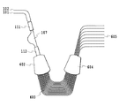
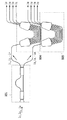
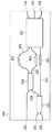
本発明の第2の実施形態における光合分波回路を図14に示す。この回路は、出力位相差が透過帯域の波長に対して各々異なる二つの位相生成光結合器111,112と、これら2個の位相生成光結合器に挟まれた1つの光路長差付与手段107と、位相生成光結合器111,112に接続するそれぞれ二本の入出力光導波路101,102と103,104より構成されている。
(Second embodiment of reference example )
An optical multiplexing / demultiplexing circuit according to the second embodiment of the present invention is shown in FIG. This circuit includes two phase generation
また、二つの位相生成光結合器111,112は、例えば、図15に示すように、4つの光結合器201〜204と、隣接する光結合器201〜204に挟まれた3つの光路長差付与部分205〜207より構成されている。
In addition, the two phase generation
この合分波回路の透過特性は、波長軸上において概ね等周期であり、波長軸上で概ね周期的になるよう等波長間隔と等周波数間隔のずれが光路長差付与手段と、出力の位相差が合分波回路の透過帯域に対して異なる位相生成光結合器により補正されている。 The transmission / reception characteristics of the multiplexing / demultiplexing circuit are substantially equal on the wavelength axis, and the shift between the equal wavelength interval and the equal frequency interval is substantially periodic on the wavelength axis. The phase difference is corrected by a phase generation optical coupler different from the transmission band of the multiplexing / demultiplexing circuit.
光干渉回路の特性は、一般に光路長差付与手段の光路長に依存し、作製誤差により光路長が設定値よりずれれば、設定通りの特性が得られない。そこで、本実施形態の光合分波回路は、光路長差付与手段の光路長を精度良く設定するため、光路長差付与手段に位相調整手段を備えている。 The characteristics of the optical interference circuit generally depend on the optical path length of the optical path length difference providing means. If the optical path length deviates from a set value due to a manufacturing error, the characteristics as set cannot be obtained. Therefore, the optical multiplexing / demultiplexing circuit of this embodiment includes a phase adjusting unit in the optical path length difference providing unit in order to set the optical path length of the optical path length difference providing unit with high accuracy.
図14に示すように、等波長間隔のマッハツェンダ干渉計の光路長差付与手段107に位相調整手段401を備えており、位相調整を行うことにより光路長差ΔL’=ΔL+αを変化させることができる。
As shown in FIG. 14, the optical path length
また、図15に示すマッハツェンダ干渉計を構成する位相生成光結合器の光路長差付与部分205〜207に位相調整手段401を備えており、位相調整を行うことにより光路長差δ1、δ2、δ3を変化させることができる。
Further, phase adjustment means 401 is provided in the optical path length
最小二乗曲線近似により、位相調整量(位相補正量)として、Ψ≒8.12×10⁻⁶λ2−0.025λ+19.2が得られた。 By the least square curve approximation, Ψ≈8.12 × 10 −6 λ 2 −0.025λ + 19.2 was obtained as a phase adjustment amount (phase correction amount).
このような位相特性を与える位相生成光結合器111,112を構成する光結合器201,202,203,204は、結合率がそれぞれr1=82%、r2=82%、r3=82%、r4=82%の方向性結合器を用いるとし、光路長差付与部205,206,207の光学的光路長差をそれぞれ位相調整手段で調整することにより、光路長差δ1=−1.13λc、δ2=0.24λc、δ3=1.13λcに設定した。
The
また、マッハツェンダ干渉計の光路長差付与手段107の光学的光路長差は位相調整手段で調整することによりΔL’=ΔL+α(ΔL=55.9μm、α=3.5・λc)となるよう設定した。 Further, the optical path length difference of the optical path length difference providing means 107 of the Mach-Zehnder interferometer is adjusted to be ΔL ′ = ΔL + α (ΔL = 55.9 μm, α = 3.5 · λ c ) by adjusting the phase adjusting means. Set.
その結果、既に図13に示した特性のように、等波長間隔と等周波数間隔のずれが補正され、これにより、透過特性は全波長範囲でCWDMグリッドにほぼ一致させることができた。また、透過特性の波長依存性は小さく、全波長領域にわたってクロストークも良好である。 As a result, the deviation between the equal wavelength interval and the equal frequency interval was corrected as in the characteristic already shown in FIG. 13, so that the transmission characteristic could be substantially matched with the CWDM grid in the entire wavelength range. Further, the wavelength dependence of the transmission characteristics is small, and the crosstalk is good over the entire wavelength region.
本実施形態の回路では、光路長差付与手段に位相調整手段を備えているため、位相調整により光学的光路長を任意に変化させることができる。 In the circuit of this embodiment, since the optical path length difference providing means includes the phase adjusting means, the optical optical path length can be arbitrarily changed by phase adjustment.
そこで、図16および図17に示したように、三つの光路長差付与部205,206,207における光路長差が0である位相生成光結合器111,112を用い、位相調整手段により二つの光路の光学的光路長を変化させることにより光路長差を与えても良い。
Therefore, as shown in FIGS. 16 and 17, the phase generation
位相調整は図16に示したように光路長差付与部における一方の導波路のみに行っても良いし、図17に示したように光路長差付与部の両側の導波路に行っても良い。 The phase adjustment may be performed on only one of the waveguides in the optical path length difference providing unit as illustrated in FIG. 16, or may be performed on the waveguides on both sides of the optical path length difference providing unit as illustrated in FIG. .
また、図16の光路長差付与手段107に示したように、同一導波路に位相調整手段が数箇所設けられていても良いし、位相調整手段の形状、位置も自由に設定することができる。 Further, as shown in the optical path length difference providing means 107 in FIG. 16, several phase adjusting means may be provided in the same waveguide, and the shape and position of the phase adjusting means can be freely set. .
もちろん、図15に示すように、予め光路長差を与えておき、位相調整手段により任意に光路長を変化させても良い。 Of course, as shown in FIG. 15, an optical path length difference may be given in advance, and the optical path length may be arbitrarily changed by the phase adjusting means.
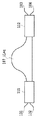
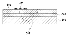
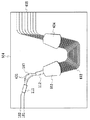
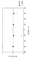
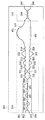
このような合分波回路は、図18に示すように、火炎堆積法、フォトリソグラフィ、反応性イオンエッチングを用いてシリコン基板504上に下部クラッド503、コア502、上部クラッド501を作製し、石英系光導波路を形成することにより作製した。また、光導波路を形成後、光導波路上に位相調整手段401として薄膜ヒータを形成した。
In such a multiplexing / demultiplexing circuit, as shown in FIG. 18, a lower clad 503, a
導波路の比屈折率差は0.75%、導波路のコア厚は7μm、コア幅は7μmとなるよう製造した。作製した回路は基板から切断した後、ファイバを接続し、モジュール化を行った。位相変化には薄膜ヒータを用い、導波路を局所加熱することにより導波路の屈折率を変化させて光学的光路長の調整を行った。 The waveguide was manufactured so that the relative refractive index difference was 0.75%, the waveguide core thickness was 7 μm, and the core width was 7 μm. The fabricated circuit was cut from the substrate, and then a fiber was connected to make a module. A thin film heater was used for phase change, and the optical path length was adjusted by changing the refractive index of the waveguide by locally heating the waveguide.
ここでは位相調整手段401として薄膜ヒータによる熱光学効果を用いる例を示したが、例えば、レーザなどによる光照射を用いても良いし、電気光学効果、磁気光学効果など位相調整ができればどのような手段を用いても良い。
Here, an example of using the thermo-optic effect by the thin film heater as the
上記実施形態で用いた導波路材料では、使用する波長帯域における屈折率の波長依存性が小さかったため、屈折率は定数であると仮定した。しかし、屈折率の波長依存性が大きい場合には、図6に示す等波長間隔と等周波数間隔の関係をあらわすグラフが変化する。その場合にも、屈折率の波長存性を考慮して波長に対する位相補正量を導出し、例えば最小二乗曲線近似により位相生成光結合器の出力の位相特性を適切に設定すれば、屈折率の波依存性も含めて、屈折率が一定の場合と同様に等波長間隔と等周波数間隔のずれを補正することができる。 In the waveguide material used in the above embodiment, since the wavelength dependence of the refractive index in the wavelength band to be used was small, the refractive index was assumed to be a constant. However, when the wavelength dependency of the refractive index is large, the graph showing the relationship between the equal wavelength interval and the equal frequency interval shown in FIG. 6 changes. Even in that case, if the phase correction amount with respect to the wavelength is derived in consideration of the wavelength existence of the refractive index and the phase characteristic of the output of the phase generation optical coupler is appropriately set by, for example, least square curve approximation, the refractive index The shift between the equal wavelength interval and the equal frequency interval can be corrected similarly to the case where the refractive index is constant, including the wave dependency.
また、上記光合分波回路では、光デバイスを実現する最低限の構成のみを説明したが、例えば、光合分波回路の偏波依存性を低減する構成としたり、温度依存性を低減する構成としてもよい。 In the above optical multiplexing / demultiplexing circuit, only the minimum configuration for realizing the optical device has been described. For example, the polarization dependency of the optical multiplexing / demultiplexing circuit is reduced, or the temperature dependency is reduced. Also good.
以上、本実施形態では、薄膜ヒータ等の位相調整手段を用い、導波路の屈折率を変化させることにより光路長差付与手段や光路長差付与部の光学的光路長差を調整し、作製誤差を軽減した。このように、位相調整手段は光学的光路長差を変化させる効果があり、光路長差付与手段として用いることにより、光合分波回路を構成する光路長差付与手段や光路長差付与部の光学的光路長差を設計どうりの値に設定することができた。これにより、等波長間隔の光合分波回路を実現することができた。 As described above, in the present embodiment, the optical path length difference of the optical path length difference providing unit and the optical path length difference providing unit is adjusted by changing the refractive index of the waveguide by using the phase adjusting unit such as a thin film heater, thereby producing a manufacturing error. Reduced. As described above, the phase adjusting unit has an effect of changing the optical path length difference, and by using it as the optical path length difference providing unit, the optical path length difference providing unit and the optical path length difference providing unit constituting the optical multiplexing / demultiplexing circuit are used. The optical path length difference could be set to the value as designed. As a result, an optical multiplexing / demultiplexing circuit having equal wavelength intervals could be realized.
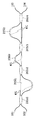
(参考例の第3の実施形態)
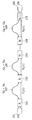
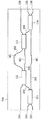
本発明の第3の実施形態における合分波回路を図19に示す。この回路は、三つの位相生成光結合器111,112,113と、これら3個の位相生成光結合器に挟まれた2つの光路長差付与手段107,108と、位相生成光結合器111に接続するそれぞれ二本の入出力光導波路101,102と、位相生成光結合器113に接続するそれぞれ二本の入出力光導波路103,104より構成されている。
(Third embodiment of reference example )
FIG. 19 shows a multiplexing / demultiplexing circuit according to the third embodiment of the present invention. This circuit includes three phase generation
ここで、光路長差付与手段107の光路長差はΔL1’=ΔL1+α1、光路長差付与手段108の光路長差はΔL2’=ΔL2+α2に設定されており、α1,α2は第1の実施形態で説明した波長オーダーの光路長である。
Here, the optical path length difference of the optical path length
また、三つの光合分波手段のうち少なくとも一つは、出力の位相差が光干渉計の透過帯域に対して異なる位相生成光結合器であり、位相成生機能を兼ねている。 In addition, at least one of the three optical multiplexing / demultiplexing means is a phase generation optical coupler having a phase difference of output different from the transmission band of the optical interferometer, and also serves as a phase generation function.
第1および第2の実施形態では、従来のマッハツェンダ干渉計の構成をもとにした位相生成機能を備えた光合分波回路であったが、本実施形態では、光路長差付与手段107,108におけるそれぞれの光路長差がΔL1=ΔL、ΔL2=2・ΔL+π、位相生成光結合器111,112,113の分岐比がそれぞれ概ね50%、70%、10%である従来のラティス・フィルタの構成(非特許文献8を参照)をもとにしている。
In the first and second embodiments, the optical multiplexing / demultiplexing circuit has a phase generation function based on the configuration of the conventional Mach-Zehnder interferometer. However, in this embodiment, the optical path length
このような光合分波回路の場合にも、第1の実施形態で説明した方法により、等周波数間隔の光合分波回路を等波長間隔にすることができる。 Also in the case of such an optical multiplexing / demultiplexing circuit, the optical multiplexing / demultiplexing circuit having equal frequency intervals can be made to have equal wavelength intervals by the method described in the first embodiment.
本実施形態の光合分波回路の透過特性の波長依存性を図20に示す。この光合分波回路は、光路長差付与手段と、出力の位相差が光合分波回路の透過帯域の波長に対して変化する位相生成光結合器を用いることにより、等波長間隔と等周波数間隔のずれが補正されている。その結果、波長軸上において概ね等周期の光合分波回路となっている。 FIG. 20 shows the wavelength dependence of the transmission characteristics of the optical multiplexing / demultiplexing circuit of this embodiment. This optical multiplexing / demultiplexing circuit uses an optical path length difference providing means and a phase generation optical coupler in which the phase difference of the output changes with respect to the wavelength of the transmission band of the optical multiplexing / demultiplexing circuit. The deviation is corrected. As a result, the optical multiplexing / demultiplexing circuit has a substantially equal period on the wavelength axis.
本実施形態の光合分波回路を構成する位相生成光結合器の一つとして、M+1個(Mは2以上の整数)の光結合器と、隣接する光結合器に挟まれたM個の光路長差付与部分を有する位相生成光結合器を用いても良い。例えば、図21の光合分波回路では、位相生成光結合器111,113としては図10に示した位相生成光結合器を用いており、位相生成光結合器112としては、マッハツェンダ型光結合器を用いている。
As one of the phase generation optical couplers constituting the optical multiplexing / demultiplexing circuit of this embodiment, M + 1 optical couplers (M is an integer of 2 or more) and M optical paths sandwiched between adjacent optical couplers. A phase generating optical coupler having a length difference providing portion may be used. For example, in the optical multiplexing / demultiplexing circuit of FIG. 21, the phase generation
また、本実施形態の光合分波手段の光路長差付与部に位相調整手段が設けられていても良い。そして、三つの光路長差付与部における光路長差がそれぞれ0である位相生成光結合器(図21の111,113)を用い、位相調整手段により二つの光路の光学的光路長を変化させることにより光路長差を与えても良い。 In addition, a phase adjusting unit may be provided in the optical path length difference providing unit of the optical multiplexing / demultiplexing unit of the present embodiment. Then, using the phase generation optical couplers (111 and 113 in FIG. 21) in which the optical path length difference in each of the three optical path length difference providing units is 0, the optical path lengths of the two optical paths are changed by the phase adjusting means. The optical path length difference may be given by
もちろん、図15に示したように予め光路長差を与えておき、位相調整手段により光路長を任意に変化させても良い。 Of course, as shown in FIG. 15, an optical path length difference may be given in advance, and the optical path length may be arbitrarily changed by the phase adjusting means.
更に、位相生成光結合器112の場合、光路長差付与部における光路長差を変化させることにより、マッハツェンダ型の分岐比可変の光結合器として機能させることもできる。
Furthermore, in the case of the phase generation
このような光合分波回路は、既に図18に示したように、火炎堆積法、フォトリソグラフィ、反応性イオンエッチングを用いてシリコン基板504上に下部クラッド503、コア502、上部クラッド501を作製し、石英系光導波路を形成することにより作製した。また、光導波路を形成後、光導波路上に位相調整手段401として薄膜ヒータを形成し、導波路の比屈折率差は0.75%、導波路のコア厚は7μm、コア幅は7μmとなるよう製造した。さらに、作製した回路は基板から切断した後、ファイバを接続し、モジュール化を行った。なお、位相変化には薄膜ヒータを用い、導波路を局所加熱することにより導波路の屈折率を変化させて光路長の調整を行った。
In such an optical multiplexing / demultiplexing circuit, as shown in FIG. 18, a
ここでは、位相調整手段401として薄膜ヒータによる熱光学効果を用いる例を示したが、例えば、レーザなどによる光照射を用いても良いし、電気光学効果、磁気光学効果など位相調整ができればどのような手段を用いても良い。
Here, an example of using the thermo-optic effect by the thin film heater as the
本実施形態で用いた導波路材料では、使用する波長帯域における屈折率の波長依存性が小さかったため、屈折率は定数であると仮定した。しかし、屈折率の波長依存性が大きい場合には、図6に示した等波長間隔と等周波数間隔の関係をあらわすグラフが変化する。その場合にも、屈折率の波長依存性を考慮して波長に対する位相補正量を導出し、非線形多項式近以により位相生成光結合器の出力の位相特性を適切に設定すれば、屈折率の波長依存性も含めて、屈折率が一定の場合と同様に等波長間隔と等周波数間隔のずれを補正することができる。 In the waveguide material used in this embodiment, since the wavelength dependence of the refractive index in the wavelength band to be used was small, the refractive index was assumed to be a constant. However, when the wavelength dependency of the refractive index is large, the graph representing the relationship between the equal wavelength interval and the equal frequency interval shown in FIG. 6 changes. Even in this case, if the phase correction amount for the wavelength is derived in consideration of the wavelength dependence of the refractive index, and the phase characteristic of the output of the phase generating optical coupler is appropriately set by the proximity of the nonlinear polynomial, the wavelength of the refractive index The shift between the equal wavelength interval and the equal frequency interval can be corrected in the same manner as when the refractive index is constant, including the dependency.
また、上記の光合分波回路では、光デバイスを実現する最低限の構成のみを説明したが、例えば、光合分波回路の偏波依存性を低減する構成としてもよく、温度依存性を低減する構成としてもよい。 In the optical multiplexing / demultiplexing circuit described above, only the minimum configuration for realizing the optical device has been described. However, for example, the polarization dependency of the optical multiplexing / demultiplexing circuit may be reduced, and the temperature dependency may be reduced. It is good also as a structure.
本実施形態では、本発明をラティス・フィルタに適用することにより、マッハツェンダ干渉計以外の干渉回路にも適用可能であることを示したが、例えば、ラティス・フィルタ以外にも、多段マッハツェンダ干渉回路、トランスバーサル・フィルタ等、その他の干渉回路であっても本発明は適用可能である。また、1入力2出力の干渉回路だけでなく、任意本数の入出力を持つ干渉回路に適用することができる。 In the present embodiment, by applying the present invention to a lattice filter, it has been shown that the present invention can also be applied to an interference circuit other than a Mach-Zehnder interferometer.For example, in addition to a lattice filter, a multistage Mach-Zehnder interference circuit, The present invention can also be applied to other interference circuits such as a transversal filter. Further, the present invention can be applied not only to a 1-input 2-output interference circuit but also to an interference circuit having an arbitrary number of inputs and outputs.
このように、本実施形態の合分波回路を用いることにより、等波長間隔の合分波回路が実現できた。 As described above, by using the multiplexing / demultiplexing circuit of this embodiment, an multiplexing / demultiplexing circuit having equal wavelength intervals can be realized.
(参考例の第4の実施形態)
本発明の第4の実施形態における光合分波回路を図22に示す。この回路は、二つの位相生成光結合器111,112と、これら2個の位相生成光結合器に挟まれた1つの光路長差付与手段107と、位相生成光結合器111に接続する入力導波路101,102より構成されている干渉回路において、位相生成光結合器112の二つの出力がアレイ導波路603と、アレイ導波路の両側に設けられた第一スラブ導波路602及び第二スラブ導波路604と、第二スラブ導波路に結合する8つの出力導波路605より構成されるアレイ導波路回折格子の第一スラブ導波路602に入射されている。
(Fourth embodiment of reference example )
An optical multiplexing / demultiplexing circuit according to the fourth embodiment of the present invention is shown in FIG. This circuit includes two phase generation
なお、干渉回路の二つの出力導波路を第一スラブ導波路602に接続する場合は、その接点の形状は任意であり、例えばテーパ導波路など形状が変化する光導波路がスラブ導波路に接続されていても良い。
Note that when the two output waveguides of the interference circuit are connected to the
ここで、光合分波手段のうち少なくとも1つは、出力の位相差が光合分波回路の透過域にある光に対して異なる位相を生成する位相生成手段であり、同時に、光結合器としても機能する位相生成光結合器である。 Here, at least one of the optical multiplexing / demultiplexing means is a phase generating means for generating a different phase with respect to the light whose output phase difference is in the transmission region of the optical multiplexing / demultiplexing circuit. It is a functioning phase generating optical coupler.
本実施形態の光合分波回路は、従来のマッハツェンダ干渉回路の二つの出力をアレイ導波路回折格子の第一スラブ導波路に入射させる構成(特許文献1参照)をもとにしている。従来の構成の場合、前段に設けられた干渉回路は等周波数間隔であったため等波長間隔のシステムに用いるには適していなかった。しかし、本実施形態で示す構成のように、前段に等波長間隔の合分波回路を用いれば、後段のアレイ導波路回折格子の出力波長間隔を前段に合わせることにより、回路全体として等波長間隔の光回路となる。 The optical multiplexing / demultiplexing circuit according to the present embodiment is based on a configuration in which two outputs of a conventional Mach-Zehnder interference circuit are incident on a first slab waveguide of an arrayed waveguide diffraction grating (see Patent Document 1). In the case of the conventional configuration, since the interference circuit provided in the previous stage has an equal frequency interval, it is not suitable for use in a system having an equal wavelength interval. However, if a multiplexing / demultiplexing circuit with equal wavelength intervals is used in the previous stage as in the configuration shown in this embodiment, the output wavelength interval of the array waveguide diffraction grating in the subsequent stage is adjusted to the previous stage, so that the entire circuit has equal wavelength intervals. This is an optical circuit.
また、マッハツェンダ干渉回路を構成する位相生成光結合器112がアレイ導波路回折格子の第一スラブ導波路に結合された構成(特許文献2)をもとにした図23の構成を取ることもできる。ここで、位相生成光結合器がスラブ導波路に結合された構成とは、例えば、図10に示した位相生成光結合器を位相生成光結合器112として用いる場合は、光結合器204がスラブ導波路に直接結合されていることを指す。
Further, the configuration of FIG. 23 based on the configuration (Patent Document 2) in which the phase generating
また、例えば、位相生成光結合器111が6つの光結合器と隣接する光結合器に挟まれた5つの光路長差付与部より構成されてもよいし、位相生成光結合器112が通常の光結合器であってもよい。さらに、光結合器が方向性結合器、マルチモード干渉カプラ、可変カプラなどであってもよい。
Further, for example, the phase generation
更に、図24に示すように、前段のマッハツェンダ干渉回路の光路長差付与手段の一方、若しくは両方の導波路に位相調整手段が設けられていても良い。 Furthermore, as shown in FIG. 24, phase adjusting means may be provided in one or both of the optical path length difference providing means of the preceding Mach-Zehnder interference circuit.
位相調整手段を用いることにより、前段のマッハツェンダ干渉回路と後段のアレイ導波路回折格子の波長を合わせることができる(非特許文献9を参照) 。 By using the phase adjusting means, the wavelengths of the preceding Mach-Zehnder interference circuit and the succeeding arrayed waveguide grating can be matched (see Non-Patent Document 9).
本実施形態の光合分波回路は、火炎堆積法、フォトリソグラフィ、反応性イオンエッチングを用いて石英系光導波路をシリコン基板上に形成した。導波路の比屈折率差は0.75%、導波路のコア厚は7μm、コア幅は7μmとなるよう製造した。また、作製した回路は基板から切断した後、ファイバを接続しモジュール化を行った。 In the optical multiplexing / demultiplexing circuit of this embodiment, a quartz-based optical waveguide is formed on a silicon substrate by using a flame deposition method, photolithography, and reactive ion etching. The waveguide was manufactured so that the relative refractive index difference was 0.75%, the waveguide core thickness was 7 μm, and the core width was 7 μm. Further, the fabricated circuit was cut from the substrate, and then a fiber was connected to make a module.
前段のマッハツェンダ干渉回路の光路長差付与手段に位相調整手段401を施した後の光合分波回路を図24に示し、その透過特性を図25に示す。
FIG. 24 shows the optical multiplexing / demultiplexing circuit after the
前段の干渉回路は等波長間隔であり、後段のアレイ導波路回折格子の出力波長間隔を前段に合わせることにより、回路全体として等波長間隔の特性が得られた。また、本構成の回路は、透過帯域が平坦なため、光通信システムで用いるのに適している。 The front-stage interference circuit has an equal wavelength interval. By matching the output wavelength interval of the rear-stage arrayed waveguide diffraction grating to the previous stage, the characteristic of the equal wavelength interval was obtained as a whole circuit. Further, the circuit of this configuration is suitable for use in an optical communication system because the transmission band is flat.
本実施例で示した構成では、前段に等波長間隔のマッハツェンダ干渉回路を用いたが、これには限定されず、第3の実施形態で示したようなラティス・フィルタ型、多段マッハツェンダ型、トランスバーサル・フィルタ型、その他の干渉回路等、任意の等波長間隔の光合分波回路を使用しても良い。 In the configuration shown in the present embodiment, a Mach-Zehnder interference circuit having an equal wavelength interval is used in the previous stage, but the present invention is not limited to this, and a lattice filter type, a multi-stage Mach-Zehnder type, a transformer as shown in the third embodiment is used. Optical multiplexing / demultiplexing circuits having arbitrary equal wavelength intervals such as a versatile filter type and other interference circuits may be used.
また、後述する(第5の実施形態)光合分波回路が複数繋がれている位相生成機能を備えた光合分波器を前段に用い、その少なくとも二つの出力がアレイ導波路回折格子のスラブ導波路に入射するようにしてもよい。 (Fifth embodiment) An optical multiplexer / demultiplexer having a phase generation function in which a plurality of optical multiplexing / demultiplexing circuits are connected is used in the previous stage, and at least two outputs thereof are slab guides of the arrayed waveguide grating. You may make it inject into a waveguide.
(参考例の第5の実施形態)
本発明の第5の実施形態における光合分波回路を図26に示す。この回路は、前段の位相生成機能を備えた光合分波回路801と、位相生成機能を備えた光合分波回路801の二つの出力にそれぞれ接続された後段の位相生成機能を備えた光合分波回路802,803とにより構成されている。ここで、前段の光合分波回路は波長間隔が20nmの等波長間隔マッハツェンダ干渉回路であり、後段の光合分波回路は波長間隔が40nmの等波長間隔マッハツェンダ干渉回路である。更に、前段と後段の干渉回路で入力光が4つの出力に分波されるように位相が設定されている。
(Fifth embodiment of reference example )
FIG. 26 shows an optical multiplexing / demultiplexing circuit according to the fifth embodiment of the present invention. This circuit includes an optical multiplexing /
このように、位相生成機能を備えた光合分波回路が複数個繋がれた構成を取ることにより、1入力4出力の位相生成機能を備えた光合分波回路を実現した。もちろん、本実施形態の位相生成機能を備えた光合分波回路も、第2の実施形態で説明したように、光路長差付与手段に位相調整手段を備えていても良い。この位相調整部により光学的光路長差を調整しても良いし、例えば、位相生成機能を備えた光合分波回路802の光路長差付与手段にπの位相変化に相当する光学的光路長差を与えれば、λ1とλ3が出力されるポートが入れ替わる。
In this way, by adopting a configuration in which a plurality of optical multiplexing / demultiplexing circuits having a phase generation function are connected, an optical multiplexing / demultiplexing circuit having a 1-input / 4-output phase generation function is realized. Of course, as described in the second embodiment, the optical multiplexing / demultiplexing circuit having the phase generation function of the present embodiment may include the phase adjusting unit in the optical path length difference providing unit. The optical path length difference may be adjusted by this phase adjustment unit. For example, the optical path length difference corresponding to the phase change of π is added to the optical path length difference providing means of the optical multiplexing /
また、図26に示した前段の干渉回路の出力導波路と後段の干渉回路の入力導波路を接続する方法は一つの例であり、入出力導波路の構成を変えれば、出力される波長の出力ポートが変化する。 In addition, the method of connecting the output waveguide of the preceding stage interference circuit and the input waveguide of the subsequent stage interference circuit shown in FIG. 26 is one example. If the configuration of the input / output waveguide is changed, the wavelength of the output wavelength is changed. The output port changes.
また、本実施形態の光合分波回路は、等波長間隔マッハツェンダ干渉回路を複数接続しているが、例えば、前段に第1の実施形態で説明した等波長間隔マッハツェンダ干渉回路(波長間隔20nm)を用い、後段に第3の実施形態で説明した等波長間隔ラティス・フィルタ(波長間隔40nm)を用いても良い。 In addition, the optical multiplexing / demultiplexing circuit of the present embodiment has a plurality of equal wavelength interval Mach-Zehnder interference circuits connected. For example, the equal wavelength interval Mach-Zehnder interference circuit (wavelength interval of 20 nm) described in the first embodiment is provided in the previous stage. It is also possible to use the equal wavelength interval lattice filter (wavelength interval of 40 nm) described in the third embodiment in the subsequent stage.
このように、任意の等波長間隔合分波器回路を複数台繋ぐことにより1入力N出力の位相生成機能を備えた光合分波回路が実現できる。 In this way, an optical multiplexer / demultiplexer circuit having a 1-input N-output phase generation function can be realized by connecting a plurality of arbitrary equal wavelength interval multiplexer / demultiplexer circuits.
更に、図27に示したように、位相生成機能を備えた光合分波回路801の二つの出力にアレイ導波路回折格子804,805を接続しても良い。そうすれば、前段の位相生成機能を備えた光合分波回路801により波長が奇数と偶数チャネルに合分波され、後段のアレイ導波路回折格子804,805により個々の波長に合分波される。従って、同様に1入力N出力の位相生成機能を備えた光合分波回路が実現できる。
Further, as shown in FIG. 27, arrayed
もちろん、上記位相生成機能を備えた光合分波回路の任意の光路長差付与手段に位相調整を行っても良い。 Of course, the phase adjustment may be performed on any optical path length difference providing means of the optical multiplexing / demultiplexing circuit having the phase generation function.
(参考例の第6の実施形態)
本発明の第6の実施形態の光合分波回路を図28に示す。本回路はN+1個(Nは1以上の整数)の位相生成光結合器111〜115と、隣接する位相生成光結合器に挟まれたN個の光路長差付与手段107〜109と、1個目の位相生成光結合器111に接続された2本の入力導波路101、102と、N+1個目の位相生成光結合器115に接続された2本の出力導波路103、104より構成されるN段ラティス・フィルタである。
(Sixth embodiment of reference example )
FIG. 28 shows an optical multiplexing / demultiplexing circuit according to the sixth embodiment of the present invention. This circuit includes N + 1 (N is an integer greater than or equal to 1) phase generation
N個の光路長差付与手段107、108、109はそれぞれ2本の光遅延線より構成されており、その光学的光路長差はそれぞれΔL1+δL1、ΔL2+δL2、・・・、ΔLN+δLNに設定されている。また、位相生成光結合器111〜115には出力の位相差が透過帯域に対して波長依存性を有する位相生成光結合器を用いている。そしてこれら位相生成光結合器を位相生成手段として用いることにより、光路長差付与手段107、108、109にそれぞれ波長依存性を有する位相Ψ1(λ)、Ψ2(λ)、・・・、ΨN(λ)が作用するようにしている。これらの位相Ψ1(λ)、Ψ2(λ)、・・・、ΨN(λ)を適切に設定することにより、図28の光合分波回路の光学特性を任意に設定することができる。
Each of the N optical path length difference providing means 107, 108, 109 is composed of two optical delay lines, and the optical optical path length differences are ΔL1 + δL1, ΔL2 + δL2,..., ΔLN + δLN, respectively. Is set to The phase generation
具体例として、本実施形態では原理的に等周波数間隔である光合分波回路の透過スペクトルを等波長間隔に変換する設計手法を説明する。もちろん、本発明の第1の実施形態等で説明した手法を用いることにより、原理的に等周波数間隔である干渉回路を等波長間隔の干渉回路にすることもできるが、ここでは別の設計手法を用いることにする。 As a specific example, in the present embodiment, a design method for converting a transmission spectrum of an optical multiplexing / demultiplexing circuit having an equal frequency interval in principle into an equal wavelength interval will be described. Of course, by using the method described in the first embodiment of the present invention, an interference circuit having an equal frequency interval can be converted into an interference circuit having an equal wavelength interval in principle, but here, another design method is used. Will be used.
一般に光合分波回路、例えば位相生成光結合器と、この位相生成光結合器に結合される光路長差付与手段より構成されるN次(Nは1以上の整数)の光合分波回路(光遅延線回路)の透過特性は、この光合分波回路のインパルス応答のフーリエ変換であり、次式のように表すことができる。 In general, an optical multiplexing / demultiplexing circuit (for example, an optical multiplexing / demultiplexing circuit (N is an integer of 1 or more)) composed of a phase generation optical coupler and an optical path length difference providing unit coupled to the phase generation optical coupler (optical The transmission characteristic of the delay line circuit) is a Fourier transform of the impulse response of the optical multiplexing / demultiplexing circuit, and can be expressed as the following equation.
![]()
![]()
本実施形態では、例として透過スペクトルを等波長間隔に変換するので、次式で与えられる非線形位相Ψ(λ)を生成すればよい。 In this embodiment, since the transmission spectrum is converted into equal wavelength intervals as an example, a nonlinear phase Ψ (λ) given by the following equation may be generated.
![]()
![]()
![]()
![]()
本実施形態では、位相生成光結合器を位相生成手段として用い、このように波長依存性のある位相を発生させる光合分波手段を位相生成光結合器と呼ぶことにする。 In this embodiment, a phase generation optical coupler is used as the phase generation means, and the optical multiplexing / demultiplexing means for generating a wavelength-dependent phase in this way is called a phase generation optical coupler.
位相生成光結合器としては、光結合器と光路長差付与部より構成される干渉計型位相生成光結合器を用いても良い。具体的に、本実施形態ではM+1個(Mは1以上の整数)の光結合器と隣接する光結合器に挟まれたM個の光路長差付与部により構成されるラティス・フィルタ型の位相生成光結合器を位相生成光結合器として用いることにする。 As the phase generation optical coupler, an interferometer type phase generation optical coupler configured by an optical coupler and an optical path length difference providing unit may be used. Specifically, in the present embodiment, a lattice filter type configured by M + 1 optical couplers (M is an integer of 1 or more) and M optical path length difference adding units sandwiched between adjacent optical couplers. The phase generation optical coupler is used as a phase generation optical coupler.
本構成の位相生成光結合器を位相生成光結合器として用いる利点は、ラティス・フィルタは原理的に損失が無いこと、そしてM+1個の光結合器の分岐比(結合角)とM個の光路長差付与部の光学的光路長差を適切に設定することにより、位相生成光結合器として機能させることができることである。また、光結合器として、近接した二本の光導波路からなる方向性結合器を用いることにする。 The advantage of using the phase generation optical coupler of this configuration as a phase generation optical coupler is that the lattice filter is theoretically lossless, and the M + 1 optical coupler branching ratio (coupling angle) and M By appropriately setting the optical path length difference of the optical path length difference providing part, it is possible to function as a phase generation optical coupler. Further, as the optical coupler, a directional coupler including two adjacent optical waveguides is used.
本発明における光合分波回路のn番目の二入力二出力ラティス・フィルタ型位相生成光結合器の伝達行列は次式で表すことができる。 The transfer matrix of the n-th two-input two-output lattice filter type phase generating optical coupler of the optical multiplexing / demultiplexing circuit in the present invention can be expressed by the following equation.
で置き換えられる複素変数、Hn*(z)はHn(z)のパラ複素共役であり、上添え字*で表す通常の複素共役を用いて、
The complex variable H n * (z) is a para-complex conjugate of H n (z), using the ordinary complex conjugate represented by the superscript *
![]()
![]()
![]()
はn番目のラティス・フィルタ型位相生成光結合器のp番目の光路長差付与部の光学的光路長差、
![]()
Is the optical path length difference of the p-th optical path length difference providing unit of the n-th lattice filter type phase generating optical coupler,
![]()
はn番目のラティス・フィルタ型位相生成光結合器のp番目の光結合器の結合角であり、より詳しく説明すると波長依存性を有する振幅結合率の角度表示である。
![]()
Is the coupling angle of the p-th optical coupler of the n-th lattice filter type phase generating optical coupler, and more specifically, it is an angle display of the amplitude coupling ratio having wavelength dependency.
光合分波回路の例として、上記原理をマッハツェンダ干渉計に適用する。本発明の等波長間隔マッハツェンダ干渉計は、図29に示すようにN+1=2個の位相生成光結合器111と112と、隣接する位相生成光結合器111と112に挟まれたN=1個の光路長差付与手段107と、1個目の位相生成光結合器111に接続された2本の入力導波路101、102と、2個目の位相生成光結合器112に接続された2本の出力導波路103、104より構成されている。光路長差付与手段107は2本の光遅延線より構成されており、その光学的光路長差はΔL1+δL1に設定している。また、位相生成光結合器111と112は伝達行列がそれぞれS1、S2のM1段、M2段ラティス・フィルタ型位相生成光結合器である。
As an example of an optical multiplexing / demultiplexing circuit, the above principle is applied to a Mach-Zehnder interferometer. As shown in FIG. 29, the equal wavelength interval Mach-Zehnder interferometer of the present invention includes N + 1 = 2 phase generation
位相生成光結合器により生成される位相差で、マッハツェンダ干渉計の光路長差付与手段107に作用する位相は、式(12)を用いることにより The phase difference generated by the phase generation optical coupler and acting on the optical path length difference providing means 107 of the Mach-Zehnder interferometer is obtained by using equation (12).
![]()
![]()
![]()
![]()
位相生成光結合器の設計パラメータの導出には数値計算を行った。なお、パラメータの数が少ないほど位相生成光結合器を作製しやすくなるため、最適化の制約条件としてθ1(λ)=θ2(λ)=θ3(λ)=θ4(λ)=θ(λ)、 Numerical calculations were performed to derive the design parameters of the phase-generating optical coupler. Note that the smaller the number of parameters, the easier it is to fabricate the phase generating optical coupler. Therefore, θ 1 (λ) = θ 2 (λ) = θ 3 (λ) = θ 4 (λ) = θ (λ),
![]()
に設定した。もちろん、位相生成光結合器の設計パラメータを導出するのにこれらの制約条件は不要である。また、ラティス・フィルタ型位相生成光結合器の段数を多くするほど、そして制約条件を課さずに任意の設計パラメータを用いることにより、目的とする特性との近似度を高めることができる。しかし最適化により、上記制約条件を与えたとしても十分近似度の高い設計パラメータを導出することができた。さらに、近似しようとする位相関数に変数を導入することにより、位相生成光結合器の設計パラメータに柔軟性を持たせ、より近似を容易にすることができる。
![]()
Set to. Of course, these constraints are not necessary to derive the design parameters of the phase generating optical coupler. In addition, as the number of stages of the lattice filter type phase generating optical coupler is increased, and by using an arbitrary design parameter without imposing a constraint, the degree of approximation with the target characteristic can be increased. However, even with the above constraints, the design parameters with a sufficiently high degree of approximation could be derived by optimization. Furthermore, by introducing a variable into the phase function to be approximated, the design parameters of the phase generating optical coupler can be made flexible and approximation can be facilitated.
そのため、式(11)に示したように、近似しようとする位相関数に変数δLを取り入れた。もちろん位相生成光結合器の設計に変数は必須ではないし、これ以外の変数を用いてもよいが、δLを用いたのは、光合分波回路の光路長差付与手段の光学的光路長差をΔL´(=ΔL+δL)に設定するだけで、変数を容易に回路に反映させることができるからである。 Therefore, as shown in the equation (11), the variable δL is introduced into the phase function to be approximated. Of course, variables are not essential for the design of the phase generation optical coupler, and other variables may be used, but δL is used to determine the optical path length difference of the optical path length difference providing means of the optical multiplexing / demultiplexing circuit. This is because the variable can be easily reflected in the circuit simply by setting ΔL ′ (= ΔL + ΔL).
式(17)が式(11)に一致し、結合角が0.5になるよう位相生成光結合器を構成する光結合器の結合角と光路長差付与手段の光学的光路長差、そして変数δLを非線形多項式近似により最適化した。最適化の結果、図30(a)に示す位相差と図30(b)に示す結合角を有する位相生成光結合器を得た。位相生成光結合器の出力の位相差、すなわち、生成される位相Φ(λ)は目的とする位相Ψ(λ) Equation (17) coincides with Equation (11), and the coupling angle of the optical coupler constituting the phase generating optical coupler and the optical path length difference of the optical path length difference providing unit so that the coupling angle is 0.5, and The variable δL was optimized by nonlinear polynomial approximation. As a result of optimization, a phase generating optical coupler having the phase difference shown in FIG. 30A and the coupling angle shown in FIG. 30B was obtained. The phase difference of the output of the phase generation optical coupler, that is, the generated phase Φ (λ) is the target phase Ψ (λ)
![]()
![]()
図31に、作製した本発明の等波長間隔マッハツェンダ干渉計の模式図を示す。位相生成光結合器である位相生成光結合器111、112を構成する光結合器201〜204、301〜304の結合角はθ(λC)=0.33、位相生成光結合器111、112の光路長差付与部205、305の光学的光路長差はδl1=1.8λC、位相生成光結合器111、112の光路長差付与部206、306の光学的光路長差はδl2=0.2λC、位相生成光結合器111、112の光路長差付与部207、307の光学的光路長差は、δl3=−1.8λC に設定した。二本の光遅延線からなるマッハツェンダ干渉計の光路長差付与手段107の光学的光路長差はΔL1´(=ΔL1+δL1)に設定し、ΔL1は従来のマッハツェンダ干渉計の光路長差付与手段の光学的光路長差、光路長差付与手段に付加する光学的光路長差は、δL1=2.0λCに設定した。
FIG. 31 shows a schematic diagram of the manufactured equal wavelength interval Mach-Zehnder interferometer of the present invention. The coupling angles of the
上記合分波回路は、火炎堆積法、フォトリソグラフィ、反応性イオンエッチングを用いてシリコン基板504上に石英系光導波路を形成することにより作製した。また、光導波路を形成後、光導波路上に位相調整手段401として幅40μm、ヒータ長4mmの薄膜ヒータを形成し、これらを用いて導波路の屈折率を変化させることにより光路長差付与手段の光学的光路長差の作製誤差を補正した。
The multiplexing / demultiplexing circuit was produced by forming a silica-based optical waveguide on the
導波路の比屈折率差は1.5%、導波路のコア厚は4.5μm、コア幅は4.5μmとなるよう製造した。このマッハツェンダ干渉計が作製されたチップをダイシングにより切り出し、入力、出力導波路にはシングルモードファイバを接続し、光モジュールを組み立てた。 The waveguide was manufactured so that the relative refractive index difference was 1.5%, the core thickness of the waveguide was 4.5 μm, and the core width was 4.5 μm. The chip on which the Mach-Zehnder interferometer was fabricated was cut out by dicing, and a single mode fiber was connected to the input and output waveguides to assemble an optical module.
図32に、作製した本発明の等波長間隔マッハツェンダ干渉計光モジュールの光学特性を示す。入力導波路102より光を入力し、出力導波路103より出力された光学特性をクロス、出力導波路104より出力された光学特性をスルーと表記した。本発明の原理を適用することにより、等波長周期40nmの光合分波回路を実現した。
FIG. 32 shows the optical characteristics of the manufactured equal wavelength interval Mach-Zehnder interferometer optical module of the present invention. The optical characteristics output from the
図33に、相対波長に対しマッハツェンダ干渉計の透過帯の中心位置がCWDMグリッドからどれだけずれるかを示す。従来型のマッハツェンダ干渉計は等周波数間隔であり、等波長間隔でないため大きな軸ずれが発生することがわかる。一方、本発明の等波長間隔マッハツェンダ干渉計は等波長周期40nmであるため、軸ずれは生じない。そのため、波長領域で周期的なグリッドを用いるCWDMシステム用光合分波回路として適している。 FIG. 33 shows how much the center position of the transmission band of the Mach-Zehnder interferometer deviates from the CWDM grid with respect to the relative wavelength. It can be seen that the conventional Mach-Zehnder interferometer has an equal frequency interval and not an equal wavelength interval, so that a large axis deviation occurs. On the other hand, since the equal wavelength interval Mach-Zehnder interferometer of the present invention has an equal wavelength period of 40 nm, no axis deviation occurs. Therefore, it is suitable as an optical multiplexing / demultiplexing circuit for CWDM systems using a periodic grid in the wavelength region.
図34に相対波長に対する損失、図35に相対波長に対するクロストークを示す。従来型のマッハツェンダ干渉計では透過帯の中心位置が波長グリッドからずれるため、CWDMグリッド上において損失が増大し、クロストークも劣化するが、本発明のマッハツェンダ干渉計は透過帯の中心位置が波長グリッドに完全に一致しているため、損失とクロストークはいずれも良好である。 FIG. 34 shows the loss with respect to the relative wavelength, and FIG. 35 shows the crosstalk with respect to the relative wavelength. In the conventional Mach-Zehnder interferometer, since the center position of the transmission band is shifted from the wavelength grid, the loss increases on the CWDM grid and the crosstalk deteriorates. Therefore, both loss and crosstalk are good.
以上、本実施形態では、一つ以上の入力と二つ以上の出力を持つ位相生成光結合器と、この位相生成光結合器に結合される光路長差付与手段により構成される干渉計型光回路において、等波長間隔になるよう設計した位相を位相生成手段により光路長差付与手段に作用させることにより、等波長間隔の光合分波回路を実現した。 As described above, in this embodiment, an interferometer type light composed of a phase generation optical coupler having one or more inputs and two or more outputs, and an optical path length difference providing unit coupled to the phase generation optical coupler. In the circuit, an optical multiplexing / demultiplexing circuit having equal wavelength intervals was realized by applying a phase designed to have equal wavelength intervals to the optical path length difference providing unit by the phase generation unit.
さらに詳しく説明すると、位相生成手段として出力の位相差が透過帯域に対して異なることを特徴とする位相生成光結合器を用いた。具体的に位相生成光結合器としてラティス・フィルタ型の位相生成光結合器を用い、目的とする位相と結合角を有するよう設計パラメータを最適化することにより、位相生成光結合器として機能させることに成功した。本実施形態で説明した一連の設計手法を用いることにより、光合分波回路の一例として従来のマッハツェンダ干渉計を等波長間隔マッハツェンダ干渉計に変換した。このことは、一般の等周波数間隔の光遅延線回路を等波長間隔に変換できることを意味するものである。 More specifically, a phase generating optical coupler characterized in that the phase difference of the output is different from the transmission band is used as the phase generating means. Specifically, a lattice filter type phase generation optical coupler is used as the phase generation optical coupler, and the design parameters are optimized so as to have a target phase and coupling angle, thereby functioning as a phase generation optical coupler. succeeded in. By using the series of design methods described in the present embodiment, a conventional Mach-Zehnder interferometer is converted into an equal wavelength interval Mach-Zehnder interferometer as an example of an optical multiplexing / demultiplexing circuit. This means that a general optical delay line circuit with equal frequency intervals can be converted into equal wavelength intervals.
もちろん、目的とする特性を実現するための位相を導出し、数値計算により位相生成光結合器の設計パラメータを最適化する過程を経る上記一連の設計アルゴリズムは本発明を実現するための一つの手法であり、第一実施形態のように、目的とする光学特性になるよう透過特性より位相補正量を直接導出する手法など、その他の手法を用いても等波長間隔合分波回路を実現できる。 Of course, the above-described series of design algorithms through the process of deriving the phase for realizing the desired characteristics and optimizing the design parameters of the phase generating optical coupler by numerical calculation is one method for realizing the present invention. Thus, as in the first embodiment, the equal wavelength interval multiplexing / demultiplexing circuit can be realized by using other methods such as a method of directly deriving the phase correction amount from the transmission characteristics so as to achieve the target optical characteristics.
また、近似する位相関数は本実施形態で示した関数に限らず、得たい透過特性により任意に設定することができる。等波長間隔に限定されず、例えば、任意の波長領域では任意の波長間隔になるよう設計することができる。等波長間隔にしたのは、本発明の特徴である位相設計の一例である。さらに、位相の表し方は必ずしも一意に決まるものではなく、同じ特性を実現するのに複数の表し方が可能である。例えば、本実施形態で用いる光合分波回路は二出力のラティス・フィルタであり、いずれの出力導波路からも光信号を取り出すことができるので、m=m´/2(m´は整数)としてもよいし、その他の関数を用いても良い。 Further, the phase function to be approximated is not limited to the function shown in the present embodiment, and can be arbitrarily set depending on the transmission characteristics to be obtained. For example, it can be designed to have an arbitrary wavelength interval in an arbitrary wavelength region. The equal wavelength interval is an example of the phase design that is a feature of the present invention. Furthermore, the way of representing the phase is not necessarily determined uniquely, and a plurality of ways of representing the same characteristic can be realized. For example, the optical multiplexing / demultiplexing circuit used in the present embodiment is a two-output lattice filter, and an optical signal can be extracted from any output waveguide, so that m = m ′ / 2 (m ′ is an integer). Alternatively, other functions may be used.
以上、本実施形態は、位相生成手段を用いることにより従来型の光合分波回路の光学特性を修正できることを説明する一つの例である。 As described above, the present embodiment is an example for explaining that the optical characteristics of the conventional optical multiplexing / demultiplexing circuit can be corrected by using the phase generation means.
(他の実施形態)
(参考例の第7の実施形態)
本発明の第7の実施形態における光合分波回路を図36に示す。本回路は、N+1個(N=2)の位相生成光結合器111〜113と、隣接する位相生成光結合器に挟まれたN(N=2)個の光路長差付与手段107〜108と、1個目の位相生成光結合器111に接続された2本の入力導波路101、102と、N+1=3個目の位相生成光結合器113に接続された2本の出力導波路103、104より構成される2段ラティス・フィルタである。
(Other embodiments)
(Seventh embodiment of reference example )
FIG. 36 shows an optical multiplexing / demultiplexing circuit according to the seventh embodiment of the present invention. This circuit includes N + 1 (N = 2) phase generation
2個の光路長差付与手段107、108はそれぞれ2本の光遅延線より構成されており、その光学的光路長差はそれぞれΔL1+δL1、ΔL2+δL2に設定されている。また、位相生成光結合器111〜113には出力の位相差が透過帯域に対して波長依存性を有する位相生成光結合器を用いている。そしてこれら位相生成光結合器を位相生成手段として用いることにより、光路長差付与手段107、108にそれぞれ波長依存性を有する位相Ψ1(λ)、Ψ2(λ)が作用するようにしている。これらの位相Ψ1(λ)、Ψ2(λ)を適切に設定することにより、図36の光合分波回路の光学特性を任意に設定することができる。
The two optical path length
具体例として、本実施形態では原理的に等周波数間隔である光合分波回路の透過スペクトルを等波長間隔に変換した波長基準器を説明する。第6の実施形態で説明した位相を光路長差付与手段に作用させれば、中心波長λc、波長間隔Δλの等波長間隔の波長基準器が実現できる。本実施形態では位相生成手段として位相生成光結合器を用い、これらの位相生成光結合器を位相生成光結合器として機能させることにより、目的とする光学特性を実現する。 As a specific example, in this embodiment, a wavelength reference device in which the transmission spectrum of an optical multiplexing / demultiplexing circuit having an equal frequency interval in principle is converted to an equal wavelength interval will be described. If the phase described in the sixth embodiment is applied to the optical path length difference providing means, a wavelength reference device having equal wavelength intervals of the center wavelength λ c and the wavelength interval Δλ can be realized. In this embodiment, a phase generation optical coupler is used as the phase generation means, and these phase generation optical couplers function as the phase generation optical coupler, thereby realizing the target optical characteristics.
本実施形態では、位相生成光結合器としてラティス・フィルタ型の位相生成光結合器を用い、位相生成光結合器111と112により光路長差付与手段107に位相Ψ1(λ)、位相生成光結合器112と113により光路長差付与手段108に位相Ψ2(λ)を作用させることにする。また、基本光学的光路長差をΔLとすると、1個目の光路長差付与手段107のΔL1=ΔL、2個目の光路長差付与手段108のΔL2=ΔLに設定した。ここで、基本光学的光路長差ΔLは従来型のラティス・フィルタ型波長基準器の光路長差付与手段の光路長差に等しい。
In the present embodiment, a lattice filter type phase generation optical coupler is used as the phase generation optical coupler, and the phase generation
また、位相生成光結合器112を近接した二本の光導波路からなる方向性結合器、位相生成光結合器111と113は伝達行列がそれぞれS1、S3のM1段、M3段ラティス・フィルタ型位相生成光結合器とした。さらに、位相生成光結合器112を中心に回路全体が線対称になるよう設計し、回路パラメータ数を減らすことにより回路の作製を容易にした。もちろん、上記構成は回路構成の一例であり、位相生成光結合器111〜113をそれぞれ異なる特性を有する位相生成光結合器とするなど、その他の回路構成を用いてもよい。
位相生成光結合器111〜113の伝達行列はそれぞれ、
In addition, a directional coupler composed of two optical waveguides close to the phase generating
The transfer matrices of the phase generating
ここでは、位相生成光結合器112を中心に回路全体を線対称にしており、光路長差付与手段107と108の設計は等しいので、光路長差付与手段107のみ最適化すればよい。最適化の結果、位相生成光結合器を6段ラティス・フィルタとした。なお、パラメータの数が少ないほど位相生成光結合器を作製しやすくなるため、最適化の制約条件としてθ1,1(λ)=θ1,2(λ)=θ1,3(λ)=θ1,4(λ)=θ1,5(λ)=θ1,6(λ)=θ(λ)、
Here, the entire circuit is made symmetrical with respect to the phase generation
![]()
![]()
![]()
に設定した。
![]()
Set to.
もちろん、位相生成光結合器の設計パラメータを導出するのにこれらの制約条件は不要であるし、これ以外の制約条件を設定してもよい。また、ラティス・フィルタ型位相生成光結合器の段数を多くするほど、そして制約条件を課さずに任意の設計パラメータを用いることにより、目的とする特性との近似度を高めることができる。 Of course, these constraint conditions are not necessary for deriving the design parameters of the phase generating optical coupler, and other constraint conditions may be set. In addition, as the number of stages of the lattice filter type phase generating optical coupler is increased, and by using an arbitrary design parameter without imposing a constraint, the degree of approximation with the target characteristic can be increased.
しかし最適化により、上記制約条件を与えたとしても十分近似度の高い設計パラメータを導出することができた。さらに、近似しようとする位相関数に変数を導入することにより、位相生成光結合器の設計パラメータに柔軟性を持たせ、より近似を容易にすることができる。 However, even with the above constraints, the design parameters with a sufficiently high degree of approximation could be derived by optimization. Furthermore, by introducing a variable into the phase function to be approximated, the design parameters of the phase generating optical coupler can be made flexible and approximation can be facilitated.
そのため、近似する位相関数に変数δL1を取り入れた。もちろん位相生成光結合器の設計に変数は必須ではないし、これ以外の変数を用いてもよいが、δL1を用いたのは、光合分波回路の光路長差付与手段の光学的光路長差をΔL1´(=ΔL1+δL1)に設定するだけで、変数を容易に回路に反映させることができるからである。 For this reason, the variable δL1 is incorporated into the approximate phase function. Of course, variables are not essential for the design of the phase generation optical coupler, and other variables may be used. However, the use of δL1 is the difference between the optical path lengths of the optical path length difference providing means of the optical multiplexing / demultiplexing circuit. This is because the variable can be easily reflected in the circuit only by setting ΔL1 ′ (= ΔL1 + ΔL1).
生成される位相差Φ1(λ)と目的とする位相Ψ1 (λ)が一致し、結合角が0.3になるよう位相生成光結合器を構成する光結合器の結合角と光路長差付与部の光学的光路長差、そして変数δL1を共役勾配法により最適化した。最適化の結果、位相生成光結合器111と112により図37(a)に示す位相差Φ1(λ)を生成させ、位相Ψ1 (λ)をよく近似できている様子がわかる。同時に図37(b)に示す結合角を有する位相生成光結合器(位相生成光結合器111)を実現した。
A difference between the coupling angle and the optical path length of the optical coupler constituting the phase generating optical coupler is set so that the generated phase difference Φ1 (λ) matches the target phase Ψ1 (λ) and the coupling angle becomes 0.3. The optical path length difference of the part and the variable δL1 were optimized by the conjugate gradient method. As a result of the optimization, it is understood that the phase difference Φ1 (λ) shown in FIG. 37A is generated by the phase generation
図38に、作製した本発明の等波長間隔ラティス・フィルタ型波長基準器の模式図を示す。位相生成光結合器である位相生成光結合器111、113を構成する光結合器211〜217、311〜317の結合角はθ(λC)=0.56、位相生成光結合器111、113の光路長差付与部231、331の光学的光路長差はδl1=1.2λC、光路長差付与部232、332の光学的光路長差はδl2=0.12λC、光路長差付与部233、333の光学的光路長差はδl3=-0.2λC、光路長差付与部234、334の光学的光路長差はδl4=-0.2λC、光路長差付与部235、335の光学的光路長差はδl5=-1.2λC、光路長差付与部236、336の光学的光路長差はδl6=-1.2λCに設定した。
FIG. 38 is a schematic diagram of the produced equal wavelength interval lattice filter type wavelength reference device of the present invention. The coupling angles of the
二本の光遅延線からなるマッハツェンダ干渉計の光路長差付与手段107、108の光学的光路長差はΔL1´=ΔL2´=ΔL´(=ΔL+δL)に設定し、ΔLは従来のラティス・フィルタの光路長差付与手段の光学的光路長差、光路長差付与手段に付加する光学的光路長差はδL=-1.8λCに設定した。また、方向性結合器310の結合角は0.4に設定した。
The optical path length difference of the optical path
上記合分波回路は、火炎堆積法、フォトリソグラフィ、反応性イオンエッチングを用いてシリコン基板504上に石英系光導波路を形成することにより作製した。また、光導波路を形成後、光導波路上に位相調整手段401として幅70μm、ヒータ長8mmの薄膜ヒータを形成し、これらを用いて導波路の屈折率を変化させることにより光路長差付与手段の光学的光路長差の作製誤差を補正した。
The multiplexing / demultiplexing circuit was produced by forming a silica-based optical waveguide on the
導波路の比屈折率差は1.5%、導波路のコア厚は4.5μm、コア幅は4.5μmとなるよう製造した。このマッハツェンダ干渉計が作製されたチップをダイシングにより切り出し、入力、出力導波路には分散シフトファイバを接続し、光モジュールを組み立てた。 The waveguide was manufactured so that the relative refractive index difference was 1.5%, the core thickness of the waveguide was 4.5 μm, and the core width was 4.5 μm. The chip on which the Mach-Zehnder interferometer was fabricated was cut out by dicing, and dispersion shifted fibers were connected to the input and output waveguides to assemble an optical module.
図39(a)に従来型波長基準器、図39(b)に本発明の原理を適用した波長基準器の透過特性を示す。ここでは入力導波路102より光を入力し、出力導波路103より出力された光学特性を示す。従来型のラティス・フィルタは等周波数間隔なので、波長軸上では等間隔にすることができない。一方、本発明の原理を適用することにより、等波長周期40nmの波長基準器を実現した。
FIG. 39A shows the transmission characteristics of a conventional wavelength reference device, and FIG. 39B shows the transmission characteristics of a wavelength reference device to which the principle of the present invention is applied. Here, optical characteristics are shown in which light is input from the
図40に、相対波長に対しラティス・フィルタの透過帯の中心位置がCWDMグリッドからどれだけずれるかを示す。従来型のラティス・フィルタは等周波数間隔であり、等波長間隔でないため大きな軸ずれが発生することがわかる。一方、本発明の等波長間隔ラティス・フィルタは等波長周期40nmであるため、軸ずれは生じない。そのため、波長領域で周期的なグリッドを用いるCWDMシステム用波長基準器として適している。 FIG. 40 shows how much the center position of the transmission band of the lattice filter deviates from the CWDM grid with respect to the relative wavelength. It can be seen that the conventional lattice filter has an equal frequency interval and not an equal wavelength interval, so that a large axis deviation occurs. On the other hand, since the equal wavelength interval lattice filter of the present invention has an equal wavelength period of 40 nm, no axis deviation occurs. Therefore, it is suitable as a wavelength reference device for CWDM systems using a periodic grid in the wavelength region.
図41に、相対波長に対する損失を示す。従来型のラティス・フィルタでは透過帯の中心位置が波長グリッドからずれるため、CWDMグリッド上において損失が増大するが、本発明のラティス・フィルタは透過帯の中心位置が波長グリッドに完全に一致しているため、軸ずれによる損失は生じない。 FIG. 41 shows the loss with respect to the relative wavelength. In the conventional lattice filter, the center position of the transmission band is shifted from the wavelength grid, so that the loss increases on the CWDM grid. However, in the lattice filter of the present invention, the center position of the transmission band completely matches the wavelength grid. Therefore, there is no loss due to axial misalignment.
以上、本実施形態では、一つ以上の入力と二つ以上の出力を持つ位相生成光結合器と、この位相生成光結合器に結合される光路長差付与手段により構成される干渉計型光回路において、等波長間隔になるよう設計した位相を位相生成手段により光路長差付与手段に作用させることにより、等波長間隔の光合分波回路を実現した。さらに詳しく説明すると、位相生成手段として出力の位相差が透過帯域に対して異なることを特徴とする位相生成光結合器を用いた。具体的に位相生成光結合器としてラティス・フィルタ型の位相生成光結合器を用い、目的とする位相と結合角を有するよう設計パラメータを最適化することにより、位相生成光結合器として機能させることに成功した。具体的に光合分波回路の一例として従来のラティス・フィルタ型波長基準器を等波長間隔ラティス・フィルタ型波長基準器に変換した。 As described above, in this embodiment, an interferometer type light composed of a phase generation optical coupler having one or more inputs and two or more outputs, and an optical path length difference providing unit coupled to the phase generation optical coupler. In the circuit, an optical multiplexing / demultiplexing circuit having equal wavelength intervals was realized by applying a phase designed to have equal wavelength intervals to the optical path length difference providing unit by the phase generation unit. More specifically, a phase generating optical coupler characterized in that the phase difference of the output is different from the transmission band is used as the phase generating means. Specifically, a lattice filter type phase generation optical coupler is used as the phase generation optical coupler, and the design parameters are optimized so as to have a target phase and coupling angle, thereby functioning as a phase generation optical coupler. succeeded in. Specifically, as an example of the optical multiplexing / demultiplexing circuit, a conventional lattice filter type wavelength reference device is converted into an equal wavelength interval lattice filter type wavelength reference device.
また、近似する位相関数は得たい透過特性により任意に設定することができる。等波長間隔の波長基準器に限定されず、例えば、任意の波長領域では任意の波長間隔になるよう設計することができる。そのため、位相を適切に設定することにより、任意の位置に透過率のピーク、すなわち波長基準位置が来るような波長基準器を実現することができる。 Further, the phase function to be approximated can be arbitrarily set according to the transmission characteristic to be obtained. The wavelength reference device is not limited to the equal wavelength interval. For example, it can be designed to have an arbitrary wavelength interval in an arbitrary wavelength region. Therefore, by setting the phase appropriately, it is possible to realize a wavelength reference device in which the transmittance peak, that is, the wavelength reference position comes to an arbitrary position.
以上、本実施形態は、位相生成手段を用いることにより従来型の光合分波回路の光学特性を修正できることを説明する一つの例である。 As described above, the present embodiment is an example for explaining that the optical characteristics of the conventional optical multiplexing / demultiplexing circuit can be corrected by using the phase generation means.
(参考例の第8の実施形態)
本発明の第8の実施形態における光合分波回路を図42に示す。本回路はN+1個(N=2)の位相生成光結合器111〜113と、隣接する位相生成光結合器に挟まれたN(N=2)個の光路長差付与手段107〜108と、1個目の位相生成光結合器111に接続された2本の入力導波路101、102と、N+1=3個目の位相生成光結合器113に接続された2本の出力導波路103、104より構成される2段ラティス・フィルタである。
(Eighth embodiment of reference example )
FIG. 42 shows an optical multiplexing / demultiplexing circuit according to the eighth embodiment of the present invention. This circuit includes N + 1 (N = 2) phase generation
2個の光路長差付与手段107、108はそれぞれ2本の光遅延線より構成されており、その光学的光路長差はそれぞれΔL1+δL1、ΔL2+δL2に設定されている。また、位相生成光結合器111〜113には出力の位相差が透過帯域に対して波長依存性を有する位相生成光結合器を用いている。そしてこれら位相生成光結合器を位相生成手段として用いることにより、光路長差付与手段107、108にそれぞれ波長依存性を有する位相Ψ1(λ)、Ψ2(λ)が作用するようにしている。これらの位相Ψ1(λ)、Ψ2(λ)を適切に設定することにより、図36の光合分波回路の光学特性を任意に設定することができる。
The two optical path length
具体例として、本実施形態では原理的に等周波数間隔である光合分波回路の透過スペクトルを等波長間隔に変換したインタリーブ・フィルタを説明する。第6の実施形態で説明した位相を光路長差付与手段に作用させれば、中心波長λc、波長間隔Δλの等波長間隔のインタリーブ・フィルタを実現できる。本実施形態では位相生成手段として位相生成光結合器を用い、これらの位相生成光結合器を位相生成光結合器として機能させることにより、目的とする光学特性を実現する。 As a specific example, the present embodiment describes an interleave filter in which the transmission spectrum of an optical multiplexing / demultiplexing circuit having an equal frequency interval in principle is converted to an equal wavelength interval. If the phase described in the sixth embodiment is applied to the optical path length difference providing means, an interleave filter having an equal wavelength interval of the center wavelength λc and the wavelength interval Δλ can be realized. In this embodiment, a phase generation optical coupler is used as the phase generation means, and these phase generation optical couplers function as the phase generation optical coupler, thereby realizing the target optical characteristics.
本実施形態では、位相生成光結合器としてラティス・フィルタ型の位相生成光結合器を用い、位相生成光結合器111と112により光路長差付与手段107に位相Ψ1(λ)、位相生成光結合器112と113により光路長差付与手段108に位相Ψ2(λ)を作用させることにする。また、基本光学的光路長差をΔLとすると、1個目の光路長差付与手段107のΔL1=ΔL、2個目の光路長差付与手段108のΔL2=−2ΔLに設定した。ここで、基本光学的光路長差ΔLは従来型のラティス・フィルタ型インタリーブ・フィルタの光路長差付与手段の光路長差に等しい。
In the present embodiment, a lattice filter type phase generation optical coupler is used as the phase generation optical coupler, and the phase generation
また、図43(b)に示すように、位相生成光結合器112を近接した二本の光導波路からなる結合角0.38の方向性結合器310、位相生成光結合器111と113は伝達行列がそれぞれS1、S3のM1段、M3段ラティス・フィルタ型位相生成光結合器とした。
As shown in FIG. 43B, the
第6の実施形態で説明したように、位相生成光結合器の位相差により光路長差付与手段107と108に作用する位相Φ1(λ)、Φ2(λ)と、目的とする位相Ψ1(λ)、Ψ2(λ)がそれぞれ一致し、同時に位相生成光結合器111、113の結合角がそれぞれ0.5、0.15の光結合器として機能するよう位相生成光結合器の設計パラメータの最適化を行った。最適化の結果、図43(a)および図43(c)に示すように、位相生成光結合器111、113をそれぞれ6段、10段ラティス・フィルタ型位相生成光結合器とした。
As described in the sixth embodiment, the phases Φ1 (λ) and Φ2 (λ) acting on the optical path length
なお、パラメータの数が少ないほど位相生成光結合器を作製しやすくなるため、最適化の制約条件としてθ1,1(λ)=θ1,2(λ)=θ1,3(λ)=θ1,4(λ)=θ1,5(λ)=θ1,6(λ)=θ1(λ)、そして、θ3,1(λ)=θ3,2(λ)=θ3,3(λ)=θ3,4(λ)=θ3,5(λ)=θ3,6(λ)=θ3,7(λ)=θ3,8(λ)=θ3,9(λ)=θ3,10(λ)=θ3(λ)に設定した。 Note that the smaller the number of parameters, the easier it is to fabricate a phase generating optical coupler. Therefore , θ 1,1 (λ) = θ 1,2 (λ) = θ 1,3 (λ) = θ 1,4 (λ) = θ 1,5 (λ) = θ 1,6 (λ) = θ 1 (λ), and θ 3,1 (λ) = θ 3,2 (λ) = θ 3 , 3 (λ) = θ 3,4 (λ) = θ 3,5 (λ) = θ 3,6 (λ) = θ 3,7 (λ) = θ 3,8 (λ) = θ 3,9 (λ) = θ 3,10 (λ) = θ 3 (λ) was set.
もちろん、位相生成光結合器の設計パラメータを導出するのにこれらの制約条件は不要であるし、これ以外の制約条件を設定してもよい。また、ラティス・フィルタ型位相生成光結合器の段数を多くするほど、そして制約条件を課さずに任意の設計パラメータを用いることにより、目的とする特性との近似度を高めることができる。しかし最適化により、上記制約条件を与えたとしても十分近似度の高い設計パラメータを導出することができた。 Of course, these constraint conditions are not necessary for deriving the design parameters of the phase generating optical coupler, and other constraint conditions may be set. In addition, as the number of stages of the lattice filter type phase generating optical coupler is increased, and by using an arbitrary design parameter without imposing a constraint, the degree of approximation with the target characteristic can be increased. However, even with the above constraints, the design parameters with a sufficiently high degree of approximation could be derived by optimization.
さらに、近似しようとする位相関数に変数を導入することにより、位相生成光結合器の設計パラメータに柔軟性を持たせ、より近似を容易にすることができる。そのため、近似する位相関数Ψ1(λ)、Ψ2(λ)にそれぞれ変数δL1、δL2を取り入れた。もちろん位相生成光結合器の設計に変数は必須ではないし、これ以外の変数を用いてもよいが、δL1、δL2を用いたのは、光合分波回路の光路長差付与手段107、108の光学的光路長差をそれぞれΔL1´(=ΔL1+δL1)、ΔL2´(=ΔL2+δL2)に設定するだけで、変数を容易に回路に反映させることができるからである。
Furthermore, by introducing a variable into the phase function to be approximated, the design parameters of the phase generating optical coupler can be made flexible and approximation can be facilitated. For this reason, the variables δL1 and δL2 are incorporated in the approximate phase functions ψ1 (λ) and ψ2 (λ), respectively. Of course, variables are not essential for the design of the phase generation optical coupler, and other variables may be used. However, δL1 and δL2 are used because the optical path length
まず、生成される位相差Φ1(λ)と目的とする位相Ψ1 (λ)が一致し、結合角が0.5になるよう位相生成光結合器を構成する光結合器の結合角と光路長差付与部の光学的光路長差、そして変数δL1を共役勾配法により最適化した。最適化の結果、位相生成光結合器111と112により図44(a)に示す位相差Φ1(λ)を生成させ、位相Ψ1 (λ)をよく近似できている様子がわかる。同時に図44(b)に示す結合角を有する位相生成光結合器(位相生成光結合器111)を実現した。
First, the coupling angle and optical path length of the optical coupler constituting the phase generating optical coupler so that the generated phase difference Φ1 (λ) matches the target phase Ψ1 (λ) and the coupling angle becomes 0.5. The optical path length difference of the difference giving part and the variable δL1 were optimized by conjugate gradient method. As a result of the optimization, it is understood that the phase difference Φ1 (λ) shown in FIG. 44A is generated by the phase generation
次に、生成される位相差Φ2(λ)と目的とする位相Ψ2 (λ)が一致し、結合角が0.15になるよう位相生成光結合器を構成する光結合器の結合角と光路長差付与部の光学的光路長差、そして変数δL2を共役勾配法により最適化した。 Next, the coupling angle and the optical path of the optical coupler constituting the phase generating optical coupler so that the generated phase difference Φ 2 (λ) matches the target phase Ψ 2 (λ) and the coupling angle becomes 0.15. The optical path length difference of the length difference imparting part and the variable δL2 were optimized by conjugate gradient method.
最適化の結果、位相生成光結合器112と113により図45(a)に示す位相差Φ2(λ)を生成させ、位相Ψ2 (λ)をよく近似できている様子がわかる。同時に図45(b)に示す結合角を有する位相生成光結合器(位相生成光結合器113)を実現した。
As a result of the optimization, it can be seen that the phase difference Φ 2 (λ) shown in FIG. 45A is generated by the phase generation
位相生成光結合器である位相生成光結合器111、113を構成する光結合器211〜217、311〜321の結合角はそれぞれ
The coupling angles of the
![]()
![]()
![]()
に設定した。また、位相生成光結合器111の光路長差付与部231、232、233、234、235、236の光学的光路長差は
![]()
Set to. Further, the optical path length difference of the optical path length
![]()
![]()
![]()
![]()
![]()
![]()
![]()
![]()
![]()
![]()
![]()
に設定した。さらに、位相生成光結合器113の光路長差付与部331、332、333、334、335、336、337、338、339、340の光学的光路長差は
![]()
Set to. Furthermore, the optical path length difference of the optical path length
![]()
![]()
![]()
![]()
![]()
![]()
![]()
![]()
![]()
![]()
![]()
![]()
![]()
![]()
![]()
![]()
![]()
![]()
![]()
に設定した。
![]()
Set to.
二本の光遅延線からなるマッハツェンダ干渉計の光路長差付与手段107、108の光学的光路長差はそれぞれΔL1´=ΔL+δL1、ΔL2´=−2ΔL+δL2に設定し、ΔLは従来のラティス・フィルタの光路長差付与手段の光学的光路長差、光路長差付与手段に付加する光学的光路長差は
The optical path length difference of the optical path length
![]()
![]()
![]()
に設定した。また、方向性結合器310の結合角は0.38である。
![]()
Set to. The coupling angle of the
上記合分波回路は、火炎堆積法、フォトリソグラフィ、反応性イオンエッチングを用いてシリコン基板504上に石英系光導波路を形成することにより作製した。また、光導波路を形成後、光導波路上に位相調整手段401として幅40μm、ヒータ長5mmの薄膜ヒータを形成し、これらを用いて導波路の屈折率を変化させることにより光路長差付与手段の光学的光路長差の作製誤差を補正した。
The multiplexing / demultiplexing circuit was produced by forming a silica-based optical waveguide on the
導波路の比屈折率差は1.5%、導波路のコア厚は4.5μm、コア幅は4.5μmとなるよう製造した。このマッハツェンダ干渉計が作製されたチップをダイシングにより切り出し、入力、出力導波路にはシングルモードファイバを接続し、光モジュールを組み立てた。 The waveguide was manufactured so that the relative refractive index difference was 1.5%, the core thickness of the waveguide was 4.5 μm, and the core width was 4.5 μm. The chip on which the Mach-Zehnder interferometer was fabricated was cut out by dicing, and a single mode fiber was connected to the input and output waveguides to assemble an optical module.
図46に、本発明の原理を適用したラティス型インタリーブ・フィルタの透過特性を示す。ここでは入力導波路102より光を入力し、出力導波路103より出力された光学特性をクロス、出力導波路104より出力された光学特性をスルーと表記した。本発明の原理を適用することにより、等波長周期40nm、すなわちチャネル間隔20nmの等波長間隔インタリーブ・フィルタを実現した。
FIG. 46 shows transmission characteristics of a lattice type interleave filter to which the principle of the present invention is applied. Here, the optical characteristic input from the
本発明の等波長間隔インタリーブ・フィルタはCWDMグリッドからの軸ずれがないので、軸ずれによる損失、クロストークが生じず、CWDMグリッド用の光合分波回路として最適である。 Since the equal wavelength interval interleave filter of the present invention has no axis deviation from the CWDM grid, loss due to axis deviation and crosstalk do not occur, and it is optimal as an optical multiplexing / demultiplexing circuit for the CWDM grid.
以上、本実施形態では、一つ以上の入力と二つ以上の出力を持つ位相生成光結合器と、この位相生成光結合器に結合される光路長差付与手段により構成される干渉計型光回路において、等波長間隔になるよう設計した位相を位相生成手段により光路長差付与手段に作用させることにより、等波長間隔の光合分波回路を実現した。 As described above, in this embodiment, an interferometer type light composed of a phase generation optical coupler having one or more inputs and two or more outputs, and an optical path length difference providing unit coupled to the phase generation optical coupler. In the circuit, an optical multiplexing / demultiplexing circuit having equal wavelength intervals was realized by applying a phase designed to have equal wavelength intervals to the optical path length difference providing unit by the phase generation unit.
さらに詳しく説明すると、位相生成手段として出力の位相差が透過帯域に対して異なることを特徴とする位相生成光結合器を用いた。具体的に位相生成光結合器としてラティス・フィルタ型の位相生成光結合器を用い、目的とする位相と結合角を有するよう設計パラメータを最適化することにより、位相生成光結合器として機能させることに成功した。具体的に光合分波回路の一例として従来のラティス・フィルタ型インタリーブ・フィルタを等波長間隔ラティス・フィルタ型インタリーブ・フィルタに変換した。 More specifically, a phase generating optical coupler characterized in that the phase difference of the output is different from the transmission band is used as the phase generating means. Specifically, a lattice filter type phase generation optical coupler is used as the phase generation optical coupler, and the design parameters are optimized so as to have a target phase and coupling angle, thereby functioning as a phase generation optical coupler. succeeded in. Specifically, as an example of an optical multiplexing / demultiplexing circuit, a conventional lattice filter type interleave filter is converted into an equal wavelength interval lattice filter type interleave filter.
本発明の光合分波回路は単体でも使用することができるが、本発明の第4の実施形態で説明したようにアレイ導波路格子などその他の光回路を本実施形態の光合分波回路に接続して使用してもよいし、同一チップ上にアレイ導波路格子などの光回路と一体集積し、光合分波モジュールとしてもよい。このように、本発明の等波長間隔合分波回路を従来の光回路と組み合わせても良い。 The optical multiplexing / demultiplexing circuit of the present invention can be used alone, but as described in the fourth embodiment of the present invention, other optical circuits such as an arrayed waveguide grating are connected to the optical multiplexing / demultiplexing circuit of the present embodiment. Or an optical multiplexing / demultiplexing module integrated with an optical circuit such as an arrayed waveguide grating on the same chip. Thus, the equal wavelength interval multiplexing / demultiplexing circuit of the present invention may be combined with a conventional optical circuit.
因みに、アレイ導波路格子は光合分波手段(スラブ導波路)と光路長差付与手段(アレイ導波路) より構成される干渉回路であるが、本発明の各実施形態で用いる光遅延線回路とは異なる原理で動作する光回路である。そのため透過特性は異なるものであり、アレイ導波路格子の透過特性は通常、等波長間隔である。なお、アレイ導波路格子は本発明と異なる手法を用いることにより等周波数間隔にできることが知られている。 Incidentally, the arrayed waveguide grating is an interference circuit composed of optical multiplexing / demultiplexing means (slab waveguide) and optical path length difference providing means (array waveguide), but the optical delay line circuit used in each embodiment of the present invention Are optical circuits operating on different principles. Therefore, the transmission characteristics are different, and the transmission characteristics of the arrayed waveguide grating are usually at equal wavelength intervals. It is known that the arrayed waveguide grating can be spaced at equal frequency by using a method different from the present invention.
また、従来のラティス型インタリーブ・フィルタにおいて、クロストークと波長分散を低減するため、回路を多段に接続する手法が報告されている。図47に示すように、本発明の等波長間隔合分波回路を縦列接続することにより、同様の効果が得られる。光信号を入力導波路103から入力した場合、出力導波路122と124から出力されるよう回路を構成している。また、前段の光合分波回路801と後段の光合分波回路802、803で中心波長が半波長異なるように回路を設計している。もちろん、これ以外の入出力ポートを使用してもよいし、多段に接続する方法も多数あり、本発明の光合分波回路を任意の構成で多段に接続しても良い。
In addition, in a conventional lattice type interleave filter, a method of connecting circuits in multiple stages has been reported in order to reduce crosstalk and chromatic dispersion. As shown in FIG. 47, the same effect can be obtained by cascading equal wavelength interval multiplexing / demultiplexing circuits of the present invention. When an optical signal is input from the
また、第5の実施形態で説明したように、前段の光合分波回路801と後段の光合分波回路802、803の波長間隔が2倍異なるようにすれば、等波長間隔の1×4インタリーブ・フィルタが実現できる。もちろん、任意のP入力Q出力合分波回路を構成することができる。
Further, as described in the fifth embodiment, if the wavelength interval between the optical multiplexing /
以上、本実施形態は、位相生成手段を用いることにより従来型の光合分波回路の光学特性を修正できることを説明する一つの例である。 As described above, the present embodiment is an example for explaining that the optical characteristics of the conventional optical multiplexing / demultiplexing circuit can be corrected by using the phase generation means.
(第9の実施形態)
本発明の各実施形態では主に波長領域で使用する光合分波回路を説明してきたが、本発明の原理は波長領域だけではなく、光周波数領域にも適用することができる。本実施形態では、その具体的な一例を示す。
(Ninth embodiment)
In each embodiment of the present invention, the optical multiplexing / demultiplexing circuit used mainly in the wavelength region has been described. However, the principle of the present invention can be applied not only to the wavelength region but also to the optical frequency region. In this embodiment, a specific example is shown.
第6の実施形態で説明したように、光合分波手段と光路長差付与手段より構成される光遅延線回路の透過特性は下記式のように表すことができる。 As described in the sixth embodiment, the transmission characteristic of the optical delay line circuit constituted by the optical multiplexing / demultiplexing means and the optical path length difference providing means can be expressed by the following equation.
具体的には、光路長差ΔLは次の二式により光周波数間隔Δfと中心光周波数fcに関連している。 Specifically, the optical path length difference ΔL is related to the optical frequency spacing Δf and the center optical frequency f c by the following two formulas.
![]()
![]()
具体的に、光周波数間隔800GHzの従来型マッハツェンダ干渉計の透過特性の透過帯の中心位置が光周波数グリッドからどれだけずれるかを図48(a)および図48(b)に示す。ただし、ここで光周波数グリッドとは、中心光周波数191THz、光周波数間隔800GHzのグリッドと仮定する。 Specifically, FIGS. 48A and 48B show how much the center position of the transmission band of the transmission characteristics of the conventional Mach-Zehnder interferometer with an optical frequency interval of 800 GHz is shifted from the optical frequency grid. Here, the optical frequency grid is assumed to be a grid having a central optical frequency of 191 THz and an optical frequency interval of 800 GHz.
図48(a)は式(25)を用いて設計した場合の軸ずれ量、図48(b)は式(26)を用いて設計した場合の軸ずれ量である。図48(a)では光周波数間隔を800GHzに設定しているので、各光周波数において軸ずれ量は一定だが、中心光周波数を設定できないので、光周波数グリッドからの軸ずれは大きい。一方、図48(b)では中心光周波数を191THzに設定しているので、中心光周波数では光周波数グリッドからのずれは零であるが、光周波数間隔を設定できないので、中心光周波数から離れるほど光周波数グリッドからの軸ずれは大きくなる。 FIG. 48A shows the amount of axial deviation when designed using equation (25), and FIG. 48B shows the amount of axial deviation when designed using equation (26). In FIG. 48A, since the optical frequency interval is set to 800 GHz, the amount of axial deviation is constant at each optical frequency, but the center optical frequency cannot be set, so the axial deviation from the optical frequency grid is large. On the other hand, in FIG. 48B, since the center optical frequency is set to 191 THz, the deviation from the optical frequency grid is zero at the center optical frequency, but the optical frequency interval cannot be set. Axis deviation from the optical frequency grid increases.
このように、従来型の光遅延線回路は一般に光周波数間隔Δfと中心光周波数fcのどちらか一方のみ自由に設定でき、両者を同時に任意の値に設定することはできない。もちろん、特殊な場合として Thus, conventional optical delay line circuit can generally either only freely set the optical frequency interval Δf and the center optical frequency f c, it can not be set to any value both at the same time. Of course, as a special case
![]()
(msは整数)を満たすなら光周波数間隔Δfと中心光周波数fcを同時に設定することができるが、このような特殊な場合に限られる。
![]()
(Ms is an integer) only if it is possible to set the optical frequency interval Δf and the center optical frequency f c it meets at the same time, a such special.
本実施形態では、光周波数依存性を有する位相生成手段を応用することにより、光周波数間隔Δfと中心光周波数fcを同時に任意の値に設定できることを示す。本発明の光遅延線回路の透過特性は、 In the present embodiment, by applying the phase generating means having an optical frequency dependence, indicating that the optical frequency interval Δf and the center optical frequency f c can be set at the same time to any value. The transmission characteristics of the optical delay line circuit of the present invention are as follows:
以上説明した原理を光遅延線回路の例としてマッハツェンダ干渉計に適用し、任意の光周波数間隔と中心光周波数を有する等周波数間隔光遅延線回路を実現できることを示す。本実施形態では位相生成手段として位相生成光結合器を用いることにより、光周波数依存性のある位相を発生させ、目的とする光学特性を実現する。 The principle described above is applied to a Mach-Zehnder interferometer as an example of an optical delay line circuit, and it is shown that an equal frequency interval optical delay line circuit having an arbitrary optical frequency interval and a center optical frequency can be realized. In this embodiment, by using a phase generation optical coupler as the phase generation means, a phase having an optical frequency dependency is generated, and a target optical characteristic is realized.
具体的に式(28)で表される位相を光周波数間隔800GHzのマッハツェンダ干渉計の光路長差付与手段に作用させた場合に、透過特性の透過帯の中心位置が光周波数グリッドからどれだけずれるかを図49に示す。中心光周波数191THz、光周波数間隔800GHzに設定しているので、光周波数グリッドと完全に一致し、光周波数グリッドからの軸ずれを解消できることがわかる。 Specifically, when the phase represented by the equation (28) is applied to the optical path length difference providing means of the Mach-Zehnder interferometer having the optical frequency interval of 800 GHz, the center position of the transmission band of the transmission characteristics is deviated from the optical frequency grid. This is shown in FIG. Since the center optical frequency is set to 191 THz and the optical frequency interval is set to 800 GHz, it can be seen that the optical frequency grid is completely coincident with the axial shift from the optical frequency grid.
位相生成光結合器として光結合器と光路長差付与部より構成される干渉計型位相生成光結合器を用いた。具体的に、本実施形態ではM+1個(Mは1以上の整数)の光結合器と隣接する光結合器に挟まれたM個の光路長差付与部により構成されるラティス・フィルタ型の光合分波手段を位相生成手段として用いることにする。 As the phase generation optical coupler, an interferometer type phase generation optical coupler composed of an optical coupler and an optical path length difference providing unit was used. Specifically, in the present embodiment, a lattice filter type configured by M + 1 optical couplers (M is an integer of 1 or more) and M optical path length difference adding units sandwiched between adjacent optical couplers. These optical multiplexing / demultiplexing means are used as phase generating means.
本構成の光合分波手段を位相生成手段として用いる利点は、ラティス・フィルタは原理的に損失が無いこと、そしてM+1個の光結合器の分岐比(結合角)とM個の光路長差付与部の光学的光路長差を適切に設定することにより、位相生成光結合器として機能させることができることである。また、光結合器として、近接した二本の光導波路からなる方向性結合器を用いることにする。 Advantages of using the optical multiplexing / demultiplexing means of this configuration as the phase generating means are that the lattice filter is theoretically lossless, and the branching ratio (coupling angle) of M + 1 optical couplers and M optical path lengths. By appropriately setting the optical path length difference of the difference providing unit, it is possible to function as a phase generation optical coupler. Further, as the optical coupler, a directional coupler including two adjacent optical waveguides is used.
本発明における光合分波回路のn番目の二入力二出力ラティス・フィルタ型位相生成光結合器の伝達行列は第6の実施形態で示した式(12)で表すことができる。ただし、zは The transfer matrix of the n-th two-input two-output lattice-filter type phase generation optical coupler of the optical multiplexing / demultiplexing circuit according to the present invention can be expressed by Expression (12) shown in the sixth embodiment. Where z is
![]()
で置き換えられる複素変数である。
![]()
Is a complex variable that is replaced by
また、式(12)のSn、p(p=1〜Mn)はp番目の光結合器と光路長差付与部からなる基本回路構成要素の伝達行列 In addition, Sn , p (p = 1 to Mn) in Expression (12) is a transfer matrix of basic circuit components including a p-th optical coupler and an optical path length difference providing unit.
![]()
はn番目のラティス・フィルタ型位相生成光結合器のp番目の光結合器の結合角であり、より詳しく説明すると光周波数依存性を有する振幅結合率の角度表示である。
![]()
Is a coupling angle of the p-th optical coupler of the n-th lattice filter type phase generating optical coupler, and more specifically, is an angle display of an amplitude coupling ratio having optical frequency dependency.
位相生成光結合器により生成される位相差で、マッハツェンダ干渉計の光路長差付与手段に作用する位相は、 The phase difference generated by the phase generation optical coupler and acting on the optical path length difference providing means of the Mach-Zehnder interferometer is:
![]()
![]()
本発明の任意光周波数間隔、中心光周波数を有するマッハツェンダ干渉計において、二つの位相生成光結合器のうち一つを位相生成光結合器としてもよいし、両方を位相生成光結合器としてもよいが、ここでは第1の実施形態で説明したように、同じ位相生成光結合器を二つ用い、マッハツェンダ干渉計の光路長差付与手段の中間点に対し、二つの位相生成光結合器が互いに線対称になるよう配置した。 In the Mach-Zehnder interferometer having an arbitrary optical frequency interval and a center optical frequency according to the present invention, one of the two phase generation optical couplers may be a phase generation optical coupler, or both may be phase generation optical couplers. However, here, as described in the first embodiment, two phase generation optical couplers are used, and the two phase generation optical couplers are mutually connected to the intermediate point of the optical path length difference providing means of the Mach-Zehnder interferometer. Arranged to be line symmetric.
このとき、H1*(z)=H2*(z)=H*(z)と−F1*(z)=F2(z)=F*(z)の関係が成立するので、式(30)は、 At this time, the relationship of H 1 * (z) = H 2 * (z) = H * (z) and −F 1 * (z) = F 2 (z) = F * (z) holds, so the equation (30)
![]()
![]()
本実施形態では、位相生成光結合器をマッハツェンダ干渉計の光路長差付与手段の中心に対し線対称に配置している。最適化の結果、位相生成光結合器を3段ラティス・フィルタとした。なお、パラメータの数が少ないほど位相生成光結合器を作製しやすくなるため、最適化の制約条件としてθ1,1(λ)=θ1,2(λ)=θ1,3(λ)=θ2,1(λ)=θ2,2(λ)=θ2,3(λ)=θ(λ)に設定した。 In the present embodiment, the phase generating optical coupler is arranged symmetrically with respect to the center of the optical path length difference providing means of the Mach-Zehnder interferometer. As a result of the optimization, the phase generation optical coupler is a three-stage lattice filter. Note that the smaller the number of parameters, the easier it is to fabricate a phase generating optical coupler. Therefore , θ 1,1 (λ) = θ 1,2 (λ) = θ 1,3 (λ) = θ 2,1 (λ) = θ 2,2 (λ) = θ 2,3 (λ) = θ (λ) was set.
もちろん、位相生成光結合器の設計パラメータを導出するのにこれらの制約条件は不要であるし、これ以外の制約条件を設定してもよい。また、マッハツェンダ干渉計の二つの位相生成光結合器を異なる設計にしてもよいし、一方のみを位相生成手段として機能させてもよい。また、ここでは位相生成機能を有する位相生成光結合器として3段ラティス・フィルタを用いたが、2段のラティス・フィルタを用いてもよいし、4段以上のラティス・フィルタを用いてもよいし、1段のラティス・フィルタ、すなわちマッハツェンダ干渉計を用いてもよい。もちろん、その他の光合分波手段を位相生成光結合器として機能させることができる。 Of course, these constraint conditions are not necessary for deriving the design parameters of the phase generating optical coupler, and other constraint conditions may be set. Further, the two phase generation optical couplers of the Mach-Zehnder interferometer may be designed differently, or only one of them may function as the phase generation means. In this example, a three-stage lattice filter is used as a phase generation optical coupler having a phase generation function. However, a two-stage lattice filter may be used, or a four-stage or more lattice filter may be used. A one-stage lattice filter, that is, a Mach-Zehnder interferometer may be used. Of course, other optical multiplexing / demultiplexing means can function as a phase generation optical coupler.
さらに、近似しようとする位相関数に変数を導入することにより、位相生成光結合器の設計パラメータに柔軟性を持たせ、より近似を容易にすることができる。そのため、近似する位相関数に変数δL1を取り入れた。もちろん位相生成光結合器の設計に変数は必須ではないし、これ以外の変数を用いてもよいが、δL1を用いたのは、光合分波回路の光路長差付与手段の光学的光路長差をΔL1´(=ΔL1+δL1)に設定するだけで、変数を容易に回路に反映させることができるからである。 Furthermore, by introducing a variable into the phase function to be approximated, the design parameters of the phase generating optical coupler can be made flexible and approximation can be facilitated. For this reason, the variable δL1 is incorporated into the approximate phase function. Of course, variables are not essential for the design of the phase generation optical coupler, and other variables may be used. However, the use of δL1 is the difference between the optical path lengths of the optical path length difference providing means of the optical multiplexing / demultiplexing circuit. This is because the variable can be easily reflected in the circuit only by setting ΔL1 ′ (= ΔL1 + ΔL1).
生成される位相差Φ1(λ)と目的とする位相Ψ1 (λ)が一致し、結合角が0.5になるよう位相生成光結合器を構成する光結合器の結合角と光路長差付与部の光学的光路長差、そして変数δL1を共役勾配法により最適化した。 The coupling angle and optical path length difference of the optical coupler constituting the phase generating optical coupler are set so that the generated phase difference Φ1 (λ) matches the target phase Ψ1 (λ) and the coupling angle becomes 0.5. The optical path length difference of the part and the variable δL1 were optimized by conjugate gradient method.
最適化の結果、位相生成光結合器111と112により図50(a)に示す位相差Φ1(λ)を生成させ、位相Ψ1 (λ)をよく近似できた。図50(b)は図50(a)の非線形部分のみを抜き出した位相であるが、位相生成光結合器により生成される位相差と目的とする位相がよく一致していることがわかる。
As a result of the optimization, the phase generation
同時に、図51に示すように位相生成光結合器を結合角0.5の光結合器として機能させることができた。 At the same time, as shown in FIG. 51, the phase generation optical coupler could function as an optical coupler having a coupling angle of 0.5.
図52に、作製した本発明のマッハツェンダ干渉計の模式図を示す。位相生成光結合器である位相生成光結合器111、112を構成する光結合器201〜204、301〜304の結合角はθ(λC)=0.3、位相生成光結合器111、112の光路長差付与部205、305の光学的光路長差はδl1=-0.2λC、光路長差付与部206、306の光学的光路長差はδl2=0.3λC、光路長差付与部207、307の光学的光路長差はδl3=0.6λCに設定した。
FIG. 52 is a schematic diagram of the manufactured Mach-Zehnder interferometer of the present invention. The coupling angles of the
二本の光遅延線からなるマッハツェンダ干渉計の光路長差付与手段107の光路長差はΔL1´=ΔL1+δL1に設定し、ΔL1は従来のマッハツェンダ干渉計の光路長差付与手段の光路長差、光路長差付与手段に付加する光路長差はδL1=-1.1λCに設定した。 The optical path length difference of the optical path length difference providing means 107 of the Mach-Zehnder interferometer comprising two optical delay lines is set to ΔL1 ′ = ΔL1 + ΔL1, where ΔL1 is the optical path length difference of the optical path length difference providing means of the conventional Mach-Zehnder interferometer. The optical path length difference added to the optical path length difference applying means was set to δL 1 = −1.1λ C.
上記合分波回路は、火炎堆積法、フォトリソグラフィ、反応性イオンエッチングを用いてシリコン基板504上に石英系光導波路を形成することにより作製した。また、光導波路を形成後、光導波路上に位相調整手段401として幅70μm、ヒータ長2mmの薄膜ヒータを形成し、これらを用いて導波路の屈折率を変化させることにより光路長差付与手段の光学的光路長差の作製誤差を補正した。
The multiplexing / demultiplexing circuit was produced by forming a silica-based optical waveguide on the
導波路の比屈折率差は0.75%、導波路のコア厚は7μm、コア幅は7μmとなるよう製造した。このマッハツェンダ干渉計が作製されたチップをダイシングにより切り出し、入力、出力導波路にはシングルモードファイバを接続し、光モジュールを組み立てた。 The waveguide was manufactured so that the relative refractive index difference was 0.75%, the waveguide core thickness was 7 μm, and the core width was 7 μm. The chip on which the Mach-Zehnder interferometer was fabricated was cut out by dicing, and a single mode fiber was connected to the input and output waveguides to assemble an optical module.
図53に、作製した本発明のマッハツェンダ干渉計光モジュールの光学特性を示す。入力導波路102より光を入力し、出力導波路103より出力された光学特性をクロス、出力導波路104より出力された光学特性をスルーと表記した。本発明の原理を適用することにより、光周波数周期800GHz、中心光周波数191THzの光合分波回路を実現した。もちろん、ITUグリッドに合うように光周波数周期を100GHz、中心光周波数を191THzに設定しても良い。
FIG. 53 shows optical characteristics of the manufactured Mach-Zehnder interferometer optical module of the present invention. The optical characteristics output from the
図54に、光周波数に対しマッハツェンダ干渉計の透過帯の中心位置が光周波数グリッド(光周波数周期800GHz、中心光周波数191THz)からどれだけずれるかを示す。本発明のマッハツェンダ干渉計に軸ずれは生じず、理論通り図49の特性を実現した。
FIG. 54 shows how much the center position of the transmission band of the Mach-Zehnder interferometer deviates from the optical frequency grid (optical frequency period 800 GHz, central
以上、本実施形態では、一つ以上の入力と二つ以上の出力を持つ位相生成光結合器と、この位相生成光結合器に結合される光路長差付与手段により構成される干渉計型光回路において、光周波数依存性を有する位相を位相生成手段により光路長差付与手段に作用させることにより、光周波数間隔と中心光周波数を同時に任意の値に設定できる光合分波回路を実現した。 As described above, in this embodiment, an interferometer type light composed of a phase generation optical coupler having one or more inputs and two or more outputs, and an optical path length difference providing unit coupled to the phase generation optical coupler. In the circuit, an optical multiplexing / demultiplexing circuit capable of simultaneously setting an optical frequency interval and a central optical frequency to arbitrary values is realized by applying a phase having optical frequency dependency to the optical path length difference providing means by the phase generating means.
さらに詳しく説明すると、位相生成手段として出力の位相差が透過帯域に対して異なる(光周波数依存性を有する)ことを特徴とする位相生成光結合器を用いた。具体的に位相生成光結合器としてラティス・フィルタ型の位相生成光結合器を用い、目的とする位相と結合角を有するよう設計パラメータを最適化することにより、位相生成光結合器として機能させることに成功した。本実施形態で説明したように、本発明は従来の光合分波回路を波長領域で使用する場合だけでなく、光周波数領域で使用する場合にも有用である。 More specifically, a phase generation optical coupler characterized in that the phase difference of the output is different from the transmission band (has optical frequency dependency) is used as the phase generation means. Specifically, a lattice filter type phase generation optical coupler is used as the phase generation optical coupler, and the design parameters are optimized so as to have a target phase and coupling angle, thereby functioning as a phase generation optical coupler. succeeded in. As described in the present embodiment, the present invention is useful not only when the conventional optical multiplexing / demultiplexing circuit is used in the wavelength domain but also when used in the optical frequency domain.
もちろん、目的とする特性を実現するための位相を導出し、数値計算により位相生成光結合器の設計パラメータを最適化する過程を経る上記一連の設計アルゴリズムは本発明を実現するための一つの手法であり、第1の実施形態のように、目的とする光学特性になるよう透過特性より位相補正量を直接導出する手法など、その他の手法を用いてもよい。 Of course, the above-described series of design algorithms through the process of deriving the phase for realizing the desired characteristics and optimizing the design parameters of the phase generating optical coupler by numerical calculation is one method for realizing the present invention. Thus, as in the first embodiment, other methods such as a method of directly deriving the phase correction amount from the transmission characteristics so as to achieve the target optical characteristics may be used.
また、近似する位相関数は本実施形態で示した関数に限らず、得たい透過特性により任意に設定することができる。任意の光周波数間隔で任意の中心光周波数を有する光合分波回路に限定されず、例えば、任意の光周波数領域では任意の光周波数間隔になるよう設計することもできる。 Further, the phase function to be approximated is not limited to the function shown in the present embodiment, and can be arbitrarily set depending on the transmission characteristics to be obtained. The present invention is not limited to an optical multiplexing / demultiplexing circuit having an arbitrary center optical frequency at an arbitrary optical frequency interval. For example, it can be designed to have an arbitrary optical frequency interval in an arbitrary optical frequency region.
さらに、位相の表し方は必ずしも一意に決まるものではなく、同じ特性を実現するのに複数の表し方が可能である。例えば、 Furthermore, the way of representing the phase is not necessarily determined uniquely, and a plurality of ways of representing the same characteristic can be realized. For example,
![]()
の時は位相を、
![]()
When the phase,
このような位相を光周波数間隔800GHzのマッハツェンダ干渉計の光路長差付与手段に作用させた場合に、透過特性の透過帯の中心位置がそれぞれ光周波数グリッドからどれだけずれるかを図55に示す。ただし、光周波数グリッドは中心光周波数190.8THz、光周波数間隔800GHzに設定している。 FIG. 55 shows how much the center position of the transmission band of the transmission characteristic is shifted from the optical frequency grid when such a phase is applied to the optical path length difference providing means of the Mach-Zehnder interferometer with an optical frequency interval of 800 GHz. However, the optical frequency grid is set to a central optical frequency of 190.8 THz and an optical frequency interval of 800 GHz.
![]()
を満たすので式(32)が有効であり、透過帯の中心位置は光周波数グリッドと完全に一致し、光周波数グリッドからの軸ずれは零であることがわかる。
![]()
Thus, it can be seen that the expression (32) is effective, the center position of the transmission band completely coincides with the optical frequency grid, and the axis deviation from the optical frequency grid is zero.
以上、本実施形態は、位相生成手段を用いることにより従来型の光合分波回路の光学特性を修正できることを説明する一つの例である。 As described above, the present embodiment is an example for explaining that the optical characteristics of the conventional optical multiplexing / demultiplexing circuit can be corrected by using the phase generation means.
(第10の実施形態)
本発明の各実施形態では主に、M+1個(Mは1以上の整数)の光結合器と隣接する光結合器に挟まれたM個の光路長差付与部により構成されるラティス・フィルタ型の光合分波手段を位相生成手段として用いた。それは、ラティス・フィルタは原理的に損失が無いこと、そしてM+1個の光結合器の分岐比(結合角)とM個の光路長差付与部の光学的光路長差を適切に設定することにより、位相生成光結合器として機能させることができることによる。また、光結合器として、近接した二本の光導波路からなる方向性結合器を用いたのは、方向性結合器の結合長を調整するだけで、結合角を変化させることができるからである。
(Tenth embodiment)
In each of the embodiments of the present invention, a lattice structure mainly composed of M + 1 optical couplers (M is an integer of 1 or more) and M optical path length difference adding units sandwiched between adjacent optical couplers. A filter type optical multiplexing / demultiplexing means was used as the phase generating means. That is, the lattice filter has no loss in principle, and the optical fiber path length difference of the M + 1 optical coupler branching ratio (coupling angle) and M optical path length difference providing units is appropriately set. By this, it can function as a phase generation optical coupler. The reason why the directional coupler composed of two adjacent optical waveguides is used as the optical coupler is that the coupling angle can be changed only by adjusting the coupling length of the directional coupler. .
しかし、位相生成手段としてラティス・フィルタを多段に接続した光合分波手段や、その他光結合器と光路長差付与部より構成される任意の干渉計型光合分波手段を用いても良い。本実施形態では、位相生成手段のその他の構成例を示す。なお、本発明の原理は位相生成手段の構成に依らずに適用できるので、位相生成手段は本発明の各実施形態の構成に限られるものではない。 However, as the phase generation means, optical multiplexing / demultiplexing means in which lattice filters are connected in multiple stages, or any other interferometer type optical multiplexing / demultiplexing means including an optical coupler and an optical path length difference providing unit may be used. In the present embodiment, another configuration example of the phase generation unit is shown. Since the principle of the present invention can be applied regardless of the configuration of the phase generation means, the phase generation means is not limited to the configuration of each embodiment of the present invention.
図56に、本発明の第10の実施形態における位相生成手段を示す。この位相生成手段はM+1個(Mは1以上の整数)の光結合器201〜204と、隣接する光結合器201〜204に挟まれたM個の光路長差付与部205〜207と、1個目の光結合器201に繋がれた入力ポートと、M+1個目の光結合器204に繋がれた出力ポートにより構成されている。光結合器201〜204として主に近接した二本の光導波路からなる方向性結合器を用いたが、もちろんマルチモード干渉カプラ、可変カプラ、X分岐カプラ、Y分岐カプラなど任意の種類のものを用いることができるし、干渉計型の光結合器を用いることもできる。ここでは、図56に示すように、干渉計型の光結合器の例として、製造偏差に対して安定な分岐比が得られる安定化光結合器(非特許文献10を参照)を用いた。
FIG. 56 shows phase generation means in the tenth embodiment of the present invention. This phase generating means includes M + 1
安定化光結合器は4つの光結合器(方向性結合器)211〜214と3組の光路長差付与部231〜233からなるラティス回路であり、回路全体で分岐要素になる。光結合器(方向性結合器)211〜214の結合角は0.5に設定されており、光路長差付与部231、232、233の光路長差はそれぞれλc/4、γ、−λc/4(λcは中心波長)に設定されている。安定化カプラの結合角はγの値を調整することで設定することができる。このような光結合器を、位相生成光結合器111を構成する光結合器201〜204として用いることにより、製造誤差に対するトレランスが大きくなる。
The stabilizing optical coupler is a lattice circuit including four optical couplers (directional couplers) 211 to 214 and three sets of optical path length
光合分波手段111を構成する光結合器、すなわち安定化カプラ201〜204の結合角と、光合分波手段111を構成する光路長差付与部205〜207の光学的光路長差を最適化することにより、製造誤差に対し安定な特性を有する位相生成光結合器を実現した。
The coupling angle of the optical couplers constituting the optical multiplexing / demultiplexing means 111, that is, the
(第10の実施形態の第1変形)
図57に、本発明の第10実施形態の第1変形における位相生成手段を示す。図の光合分波手段114は複数の光合分波手段111、112、113より構成されている。具体的には、光合分波手段111の二つの出力ポートに光合分波手段112、113が縦列接続されている。光合分波手段114は位相生成光結合器であるが、光合分波手段114を構成する光合分波手段111、112、113も位相生成光結合器である。このように、位相生成光結合器として機能する複数の光合分波手段を用いて任意のP入力Q出力(P、Qは自然数)位相生成光結合器を構成してもよい。
(First modification of the tenth embodiment)
FIG. 57 shows the phase generation means in the first modification of the tenth embodiment of the present invention. The optical multiplexing / demultiplexing means 114 shown in the figure is composed of a plurality of optical multiplexing / demultiplexing means 111, 112, 113. Specifically, optical multiplexing / demultiplexing means 112 and 113 are connected in cascade to two output ports of the optical multiplexing / demultiplexing means 111. The optical multiplexing / demultiplexing means 114 is a phase generation optical coupler, but the optical multiplexing / demultiplexing means 111, 112, 113 constituting the optical multiplexing / demultiplexing means 114 are also phase generation optical couplers. In this way, an arbitrary P input Q output (P and Q are natural numbers) phase generation optical coupler may be configured using a plurality of optical multiplexing / demultiplexing means functioning as a phase generation optical coupler.
図57の構成は4入力4出力の位相生成光結合器であるが、任意のポートを入力ポートもしくは出力ポートとして使用してもよい。また、本発明の実施形態では、位相生成光結合器の一つの入力ポートより光を入力し、二つの出力ポートより出力される光の振幅結合率(結合角)と位相差を位相生成光結合器として使用した。しかし、本実施形態のように入出力ポートの数は任意であり、例えば四つの出力ポートを有する場合は、それぞれのポートより出力される光の振幅結合率(結合角)と相対位相差を定義することができる。 The configuration of FIG. 57 is a 4-input / 4-output phase generation optical coupler, but any port may be used as an input port or an output port. In the embodiment of the present invention, light is input from one input port of the phase generation optical coupler, and the amplitude coupling ratio (coupling angle) and phase difference of the light output from the two output ports are phase generation optical coupling. Used as a vessel. However, the number of input / output ports is arbitrary as in this embodiment. For example, when there are four output ports, the amplitude coupling rate (coupling angle) and relative phase difference of light output from each port are defined. can do.
図58に、図57の位相生成光結合器114を用いた本発明の光合分波回路を示す。本回路はN+1個(N=1)の位相生成光結合器114、115と、隣接する位相生成光結合器に挟まれたN(N=1)個の光路長差付与手段107と、1個目の位相生成光結合器114に接続された4本の入力導波路101〜104と、N+1=2個目の位相生成光結合器115に接続された2本の出力導波路105、106より構成されるマッハツェンダ干渉計である。
FIG. 58 shows an optical multiplexing / demultiplexing circuit of the present invention using the phase generating
光路長差付与手段107は2本の光遅延線より構成されており、その光学的光路長差はそれぞれΔL1+δL1に設定されている。N+1=2個目の位相生成光結合器115として任意の位相生成光結合器を用いることができるが、ここでは、光結合器である方向性結合器を用いた。1個目の位相生成光結合器114には出力の位相差が透過帯域に対して波長依存性もしくは光周波数依存性を有する位相生成光結合器を用いている。そしてこの位相生成光結合器を位相生成手段として用いることにより、光路長差付与手段107に波長依存性もしくは光周波数依存性を有する位相Ψ1が作用するようにしている。この位相Ψ1を適切に設定することにより、図58の光合分波回路の光学特性を任意に設定することができた。
The optical path length
(第10の実施形態の第2変形)
図59に、本発明の第10実施形態の第2変形における位相生成手段を示す。図の位相生成光結合器111は光結合器201〜204と光遅延線251〜255より構成されている。位相生成光結合器111の構成は、広義にはトランスバーサル型光合分波回路と呼ぶことができる。
(Second modification of the tenth embodiment)
FIG. 59 shows the phase generation means in the second modification of the tenth embodiment of the present invention. The phase generation
この光合分波回路は、光結合器201と、光結合器201に接続された入力ポートと、光結合器201の一方の出力ポートに接続された光遅延線251と、光結合器201の他方の出力ポートに接続された光遅延線254と、光遅延線254に接続された光結合器202と、光結合器202に接続される光遅延線252と253と、光遅延線252と253に接続される光結合器203と、光結合器203と光遅延線251に接続される光結合器204と、光結合器204に接続される出力ポートより構成される。
This optical multiplexing / demultiplexing circuit includes an
位相生成光結合器111を構成する光結合器の結合角と光路長差付与部の光路長差を適切に設定することにより、位相生成光結合器として機能させることができる。もちろん、トランスバーサル型光合分波回路の構成法はいくつもあり、本構成はその構成例の一つである。
By appropriately setting the coupling angle of the optical coupler constituting the phase generation
図60に示す構成等も広義にはトランスバーサル型光合分波回路と呼ぶことができる。この光合分波回路は、光結合器201と、光結合器201に接続された入力ポートと、光結合器201の一方の出力ポートに接続された光遅延線251と、光結合器201の他方の出力ポートに接続された光遅延線254と、光遅延線254に接続された光結合器202と、光結合器202に接続される光遅延線252と253と、光遅延線252と253と光遅延線251に接続される光結合器203と、光結合器203に接続される3つの出力ポートより構成される。光結合器203は3入力3出力のマルチモード干渉計等で構成しても良いし、複数の光結合器で構成しても良い。位相生成光結合器111を構成する光結合器の結合角と光路長差付与部の光路長差を適切に設定することにより、位相生成光結合器として機能させることができる。
The configuration shown in FIG. 60 can also be called a transversal optical multiplexing / demultiplexing circuit in a broad sense. This optical multiplexing / demultiplexing circuit includes an
(第11の実施形態)
本発明の第11の実施形態における光合分波回路を図61に示す。本回路はN+1個(Nは1以上の整数)の光結合器211〜215と、隣接する光結合器に挟まれたN個の光路長差付与手段107〜109と、1個目の光結合器211に接続された2本の入力導波路101、102と、N+1個目の光結合器215に接続された2本の出力導波路103、104より構成されるN段ラティス・フィルタである。
(Eleventh embodiment)
FIG. 61 shows an optical multiplexing / demultiplexing circuit according to the eleventh embodiment of the present invention. This circuit includes N + 1
N個の光路長差付与手段107、108、109はそれぞれ2本の光遅延線より構成されており、その光学的光路長差はそれぞれΔL1+δL1、ΔL2+δL2、・・・、ΔLN+δLNに設定されている。また、光路長差付与手段107、108、109には透過帯域に対して波長依存性もしくは光周波数依存性を有する位相Ψ1、Ψ2、・・・、ΨNが作用している。上記位相を適切に設定することにより、図61の光合分波回路の光学特性を任意に設定することができる。波長依存性もしくは光周波数依存性を有する位相Ψ1、Ψ2、・・・、ΨNを作用させる手法として、光路長差付与手段に位相生成手段を設けた。 Each of the N optical path length difference providing means 107, 108, 109 is composed of two optical delay lines, and the optical optical path length differences are ΔL1 + δL1, ΔL2 + δL2,..., ΔLN + δLN, respectively. Is set to Further, the optical path length difference providing means 107, 108, 109 are operated with phases Ψ1, Ψ2,..., ΨN having wavelength dependency or optical frequency dependency with respect to the transmission band. By appropriately setting the phase, the optical characteristics of the optical multiplexing / demultiplexing circuit of FIG. 61 can be arbitrarily set. As a method of applying the phases Ψ1, Ψ2,..., ΨN having wavelength dependency or optical frequency dependency, phase generation means is provided in the optical path length difference providing means.
図62は、二本の光遅延線からなる光路長差付与手段107〜109のそれぞれの光遅延線に位相生成光結合器111〜116を備える様子を示す。位相生成結合器として、光結合器と光路長差付与部より構成される任意の構成の位相生成光結合器を用いることができる。
FIG. 62 shows a state in which the phase generation
図63は本実施形態の光合分波回路の簡単な例として、マッハツェンダ干渉計の模式図を示す。本回路はN+1=2個の光結合器211、216と、隣接する光結合器に挟まれたN=1個の光路長差付与手段107と、1個目の光結合器211に接続された2本の入力導波路101、102と、N+1個目の光結合器216に接続された2本の出力導波路104、105と、光路長差付与手段107の一方の光遅延線に挿入された位相生成結合器112と、位相生成結合器112に接続された入力導波路103と、位相生成結合器112に接続された出力導波路106より構成される。光路長差付与手段107には作製誤差を解消するための位相誤差調整手段401として薄膜ヒータが形成されており、二本の光遅延線と位相誤差調整手段401により、光路長差付与手段107の光学的光路長差がΔL1+δL1になるようにしている。
FIG. 63 is a schematic diagram of a Mach-Zehnder interferometer as a simple example of the optical multiplexing / demultiplexing circuit of this embodiment. This circuit is connected to N + 1 = 2
位相生成光結合器111としては、光結合器212〜215と、隣接する光結合器に挟まれた光路長差付与部231〜233より構成されるラティス型位相生成手段を用いた。そして、目的とする位相Ψ1を近似する位相Φを生成するよう、位相生成光結合器111を構成する光結合器の結合角と光路長差付与部の光学的光路長差を最適化した。
As the phase generation
位相生成光結合器112の使用していない入出力ポートは、モニターポートとして使用することができる。また、図63では位相生成光結合器111のスルーポートを使用したが、クロスポートを使用してもよい。もちろん、任意のP入力Q出力の位相生成手段を用いてよい。
An input / output port not used by the phase generation
また、図63は光遅延線に一つの位相生成手段のみを有する構成であるが、一つの光遅延線に複数の位相生成手段を有してもよいし、二本の光遅延線からなる光路長差付与手段の両方の光遅延線に位相生成手段を備えても良い。また、マッハツェンダ干渉計の位相生成光結合器を光結合器211、216としたが、図64に示すように、これらの光結合器を、位相生成機能を有する位相生成光結合器としてもよい。
FIG. 63 shows a configuration in which only one phase generation unit is provided in the optical delay line, but a plurality of phase generation units may be provided in one optical delay line, or an optical path composed of two optical delay lines. Phase generation means may be provided in both optical delay lines of the length difference providing means. Further, although the phase generation optical couplers of the Mach-Zehnder interferometer are the
以上、光合分波回路の光路長差付与手段に位相生成手段を備える構成法を説明し、簡単な例としてマッハツェンダ干渉計の具体的な構成図を示した。 The configuration method in which the phase generation unit is provided in the optical path length difference providing unit of the optical multiplexing / demultiplexing circuit has been described above, and a specific configuration diagram of the Mach-Zehnder interferometer is shown as a simple example.
(第12の実施形態)
本発明の第12の実施形態における光合分波回路を図65に示す。任意の特性を実現できる光遅延線回路としてラティス・フィルタやトランスバーサル・フィルタ等のフィルタ構成が一般に用いられているが、本実施形態で説明する多段マッハツェンダ干渉計も同様に任意の特性を実現できるフィルタ構成の一つである。
(Twelfth embodiment)
FIG. 65 shows an optical multiplexing / demultiplexing circuit according to the twelfth embodiment of the present invention. A filter configuration such as a lattice filter or a transversal filter is generally used as an optical delay line circuit capable of realizing an arbitrary characteristic, but the multistage Mach-Zehnder interferometer described in the present embodiment can also realize an arbitrary characteristic. This is one of the filter configurations.
本回路は2個の位相生成光結合器111、112と、隣接する位相生成光結合器に挟まれた1つの光路長差付与手段107より構成されるマッハツェンダ干渉計が多段に接続された構成である。1段目のマッハツェンダ干渉計の位相生成光結合器111に2本の入力導波路103、104が接続されており、位相生成光結合器112の一方には出力導波路124、他方には2段目のマッハツェンダ干渉計が接続されている。2段目のマッハツェンダ干渉計の位相生成光結合器113に1本の入力導波路102が接続されており、位相生成光結合器114の一方には出力導波路123、他方には3段目のマッハツェンダ干渉計が接続されている。3段目のマッハツェンダ干渉計の位相生成光結合器115に1本の入力導波路101が接続されており、位相生成光結合器116には二本の出力導波路121、122が接続されている。
This circuit has a configuration in which Mach-Zehnder interferometers composed of two phase generation
光路長差付与手段107、108、109の光学的光路長差はそれぞれΔL1´=ΔL+δL1、ΔL2´=2・ΔL+δL2、ΔL3´=3・ΔL+δL3に設定した。ただし、ΔLは従来のマッハツェンダ干渉計の基本光学的光路長差である。 The optical path length differences of the optical path length difference providing means 107, 108, 109 were set to ΔL1 ′ = ΔL + δL1, ΔL2 ′ = 2 · ΔL + δL2, and ΔL3 ′ = 3 · ΔL + δL3, respectively. Here, ΔL is the basic optical path length difference of the conventional Mach-Zehnder interferometer.
位相生成光結合器111と112のうちいずれか一方、もしくは両方を位相生成光結合器にし、光路長差付与手段に位相を作用させることにより1段目のマッハツェンダ干渉計の光学特性を修正でき、例えば等波長間隔にすることができる。
The optical characteristics of the first stage Mach-Zehnder interferometer can be corrected by making one or both of the phase generation
また、位相生成光結合器113と114のうちいずれか一方、もしくは両方を位相生成光結合器にし、光路長差付与手段に位相を作用させることにより2段目のマッハツェンダ干渉計の光学特性を修正でき、例えば等波長間隔にすることができる。
In addition, one or both of the phase generation
さらに、位相生成光結合器115と116のうちいずれか一方、もしくは両方を位相生成光結合器にし、光路長差付与手段に位相を作用させることにより3段目のマッハツェンダ干渉計の光学特性を修正でき、例えば等波長間隔にすることができる。多段に接続されたマッハツェンダ干渉計をそれぞれ等波長間隔になるようにすれば、回路全体として等波長間隔の光合分波回路になる。
Furthermore, one or both of the phase generation
以上、本実施形態は、位相生成手段を用いることにより従来型の光合分波回路の光学特性を修正できることを説明する一つの例である。 As described above, the present embodiment is an example for explaining that the optical characteristics of the conventional optical multiplexing / demultiplexing circuit can be corrected by using the phase generation means.
(第13の実施形態)
図66に、本発明の第13の実施形態における光合分波回路を示す。本回路は一つ以上の入力と二つ以上の出力を持つ位相生成光結合器111、112と、これらの位相生成光結合器に結合される光遅延線251〜253からなる光路長差付与手段により構成される干渉回路であり、広義のトランスバーサル型光合分波回路である。
(13th Embodiment)
FIG. 66 shows an optical multiplexing / demultiplexing circuit according to the thirteenth embodiment of the present invention. This circuit includes a phase generation
さらに詳しく説明すると、本回路は、位相生成光結合器111と、位相生成光結合器111に接続される一本以上の入力導波路101〜102と、位相生成光結合器111に接続される3本以上の光遅延線251〜253からなる光路長差付与手段と、光遅延線251〜253に接続される位相生成光結合器112と、位相生成光結合器112に接続される一本以上の出力導波路103〜104より構成されている。
More specifically, this circuit includes a phase generation
位相生成光結合器111、112は位相生成光結合器であり、単体で位相生成手段として機能させても良いし、複数の位相生成光結合器を組み合わせて一つの位相生成手段として機能させてもよい。これらの位相生成光結合器を位相生成手段として用いることにより、光路長差付与手段に波長依存性もしくは光周波数依存性を有する位相Ψを作用させることができる。この位相Ψを適切に設定することにより、図66の光合分波回路の光学特性を任意に設定することができる。
The phase generation
例えば、トランスバーサル型光合分波回路に位相生成手段を取り入れれば、本発明の各実施形態で説明した非線形多項式で近似される位相を生成することができ、波長領域で使用する干渉回路や光周波数領域で使用する干渉回路の光学特性を変形することができる。さらに、本実施形態では、干渉回路を構成する位相生成光結合器のうち少なくとも一つに、波長依存性もしくは光周波数依存性を有する位相生成機能を備えている。 For example, if phase generation means is incorporated into a transversal optical multiplexing / demultiplexing circuit, a phase approximated by the nonlinear polynomial described in each embodiment of the present invention can be generated, and an interference circuit or optical element used in the wavelength region can be generated. The optical characteristics of the interference circuit used in the frequency domain can be modified. Furthermore, in this embodiment, at least one of the phase generation optical couplers constituting the interference circuit is provided with a phase generation function having wavelength dependency or optical frequency dependency.
具体的な光合分波回路として、従来の等周波数間隔であるトランスバーサル型インタリーブ・フィルタ(特許文献3参照)の透過特性を修正し、等波長間隔のトランスバーサル型インタリーブ・フィルタに変換した。図67に示すように位相生成光結合器111、及び112として、光結合器と光路長差付与部より構成される位相生成機能付き位相生成光結合器113と114、及び115と116を複数組み合わせた位相生成光結合器を用いた。
As a specific optical multiplexing / demultiplexing circuit, the transmission characteristics of a conventional transversal interleave filter (see Patent Document 3) having an equal frequency interval are corrected and converted to a transversal interleave filter having an equal wavelength interval. As shown in FIG. 67, as the phase generation
位相生成光結合器111は、位相生成機能を有する位相生成光結合器113と、位相生成光結合器113に接続された二本の入力ポートと、位相生成光結合器113に接続された一本の出力ポートと、位相生成光結合器113に接続された位相生成機能を有する位相生成光結合器114と、位相生成光結合器114に接続された一本の入力ポートと、位相生成光結合器114に接続された二本の出力ポートより構成される。
The phase generation
位相生成光結合器112は、位相生成機能を有する位相生成光結合器115と、位相生成光結合器115に接続された二本の入力ポートと、位相生成光結合器115に接続された一本の出力ポートと、位相生成光結合器115に接続された位相生成機能を有する位相生成光結合器116と、位相生成光結合器116に接続された一本の入力ポートと、位相生成光結合器116に接続された二本の出力ポートより構成される。
The phase generation
光遅延線251の相対的な光学的光路長差を0・ΔL+0.5λcとして、光遅延線252の相対的な光学的光路長差をΔL1´=ΔL1+δL1=ΔL+δL1、光遅延線253の相対的な光学的光路長差をΔL2´=ΔL2+δL2=3・ΔL+δL2に設定した。位相生成光結合器113の結合角は0.55、位相生成光結合器114の結合角は0.22、位相生成光結合器115の結合角は0.22、そして位相生成光結合器116の結合角は0.5に設定した。また、位相生成光結合器113、114そして115、116は位相生成光結合器として用い、光遅延線252に位相Φ1(λ)、光遅延線253に位相Φ2(λ)を作用させた。
The relative optical path length difference of the
以上、本実施形態は、位相生成手段を用いることにより従来型の光合分波回路の光学特性を修正できることを説明する一つの例である。 As described above, the present embodiment is an example for explaining that the optical characteristics of the conventional optical multiplexing / demultiplexing circuit can be corrected by using the phase generation means.
(第13の実施形態の変形)
図68に、本発明の第13実施形態の変形にかかる光合分波回路を示す。本回路は一つ以上の入力と二つ以上の出力を持つ位相生成光結合器111、112と、113、114と、これらの位相生成光結合器に結合される光遅延線251〜255からなる光路長差付与手段により構成される干渉回路であり、広義のトランスバーサル型光合分波回路である。
(Modification of the thirteenth embodiment)
FIG. 68 shows an optical multiplexing / demultiplexing circuit according to a modification of the thirteenth embodiment of the present invention. This circuit comprises phase generating
さらに詳しく説明すると、本回路は位相生成光結合器と、この位相生成光結合器に接続される光遅延線が交互に接続されたトランスバーサル型光合分波回路である。また、波長依存性もしくは光周波数依存性を有する位相生成手段を、位相生成光結合器もしくは光路長差付与手段のうち少なくとも一つに備えている。 More specifically, this circuit is a transversal optical multiplexing / demultiplexing circuit in which a phase generation optical coupler and optical delay lines connected to the phase generation optical coupler are alternately connected. In addition, a phase generation unit having wavelength dependency or optical frequency dependency is provided in at least one of the phase generation optical coupler and the optical path length difference providing unit.
図68の例では、もし位相生成手段を位相生成光結合器に備えるなら、位相生成光結合器111もしくは114を、出力の位相差が透過帯域に対して異なることを特徴とする位相生成光結合器とすればよい。もし位相生成手段を光路長差付与手段に備えるなら、位相生成光結合器112もしくは113を位相生成光結合器とすればよい。
In the example of FIG. 68, if the phase generation means is provided with a phase generation optical coupler, the phase generation
例えば、光遅延線251と254は光路長差付与手段を形成しているが、光遅延線254に位相生成光結合器112が接続されているので、位相生成光結合器112を位相生成光結合器にすれば、光遅延線251と254からなる光路長差付与手段に位相生成手段を備えることができる。
For example, the
具体的な光合分波回路として、従来の等周波数間隔であるトランスバーサル型インタリーブ・フィルタの透過特性を修正し、等波長間隔のトランスバーサル型インタリーブ・フィルタに変換した。 As a specific optical multiplexing / demultiplexing circuit, the transmission characteristics of a conventional transversal interleave filter with equal frequency intervals were corrected and converted to a transversal interleave filter with equal wavelength intervals.
図69に、本実施形態の変形における光合分波回路の模式図を示す。本回路は、位相生成光結合器111と、位相生成光結合器111に接続される二本の入力導波路102、103と、位相生成光結合器111に接続される二本の光遅延線251、254と、光遅延線254に接続される位相生成光結合器112と、位相生成光結合器112に接続される一本の入力導波路101と、位相生成光結合器112に接続される二本の光遅延線252、253と、光遅延線252、253に接続される位相生成光結合器113と、位相生成光結合器113に接続される一本の出力導波路104と、位相生成光結合器113に接続される1本の光遅延線255と、光遅延線255と光遅延線251に接続される位相生成光結合器114と、位相生成光結合器114に接続される二本の出力導波路105、106より構成される。
FIG. 69 shows a schematic diagram of an optical multiplexing / demultiplexing circuit in a modification of the present embodiment. This circuit includes a phase generation
光遅延線251、252、253には位相調整手段401を設け、これらを用いて光遅延線の光学的光路長差の作製誤差を補正した。
The
また、本構成では、位相生成光結合器と光路長差付与手段の両方に位相生成手段を備えている。具体的には、位相生成光結合器111と114、そして112と113を位相生成光結合器として機能させることにより、位相生成光結合器に位相生成手段を備え、かつ光遅延線からなる光路長差付与手段に位相生成手段を備えている。
Further, in this configuration, both the phase generation optical coupler and the optical path length difference providing means are provided with phase generation means. Specifically, by causing the phase generation
光遅延線251の相対的な光学的光路長差を0・ΔL+0.5λcとして、光遅延線252の相対的な光学的光路長差を0・ΔL、光遅延線254の相対的な光学的光路長差をΔL1´=ΔL1+δL1=ΔL/2+δL1、光遅延線253の相対的な光学的光路長差をΔL2´=ΔL2+δL2=2・ΔL+δL2、光遅延線255の相対的な光学的光路長差をΔL3´=ΔL3+δL3=ΔL/2+δL3に設定した。位相生成光結合器111の結合角は0.55、位相生成光結合器112の結合角は0.22、位相生成光結合器113の結合角は0.22、そして位相生成光結合器114の結合角は0.5に設定した。また、位相生成光結合器111〜114は位相生成光結合器として用い、光遅延線254に位相Φ1(λ)、光遅延線253に位相Φ2(λ)、光遅延線255に位相Φ3(λ)を作用させた。
The relative optical path length difference of the
もちろん、図69の構成は本発明の実施例の一つであり、その他の構成を取ることもできる。例えば、図70に示すように光合分波回路を構成してもよい。本回路は一つ以上の入力と二つ以上の出力を持つ位相生成光結合器111、112と、光結合器201と、これらの位相生成光結合器もしくは光結合器に結合される光遅延線251〜254からなる光路長差付与手段により構成される干渉回路であり、広義のトランスバーサル型光合分波回路である。
Of course, the configuration of FIG. 69 is one of the embodiments of the present invention, and other configurations can be adopted. For example, an optical multiplexing / demultiplexing circuit may be configured as shown in FIG. The circuit includes phase generating
さらに詳しく説明すると、本回路は、位相生成光結合器111と、位相生成光結合器111に接続される二本の入力導波路102、103と、位相生成光結合器111に接続される二本の光遅延線251、254と、光遅延線254に接続される位相生成光結合器112と、位相生成光結合器112に接続される一本の入力導波路101と、位相生成光結合器112に接続される二本の光遅延線252、253と、光遅延線252、253と光遅延線251に接続される光結合器201と、光結合器201に接続される三本の出力導波路104、105、106より構成される。光遅延線251、252、253には位相調整部401を設け、これらを用いて光遅延線の光学的光路長差の作製誤差を補正した。
More specifically, this circuit includes a phase generation
光結合器201として3入力3出力のマルチモード干渉計カプラを用いたが、その他の光結合器を用いてもよいし、複数の光結合器を組み合わせて一つの光結合器として機能させてもよい。
Although a 3-input 3-output multi-mode interferometer coupler is used as the
位相生成光結合器111と112は位相生成光結合器として用い、光遅延線251〜254に位相を作用させて従来型の光合分波回路の光学特性を修正した。
The phase generation
(参考例の第14の実施形態)
図71(a)に本発明の第14の実施形態における光合分波回路を示す。本発明の各実施形態で説明した光合分波回路では、作製した回路の偏波依存性が小さかったため、偏波について考慮しなかった。しかし、偏波依存性が大きい場合は偏波を考慮して回路を設計・作製することにより、偏波依存性を解消することができる。反対に、偏波依存性を適切に発生させることにより、例えば偏波インタリーブ・フィルタや偏光ビームスプリッタなど偏波依存性を有する光合分波回路を実現することもできる。
(Fourteenth embodiment of reference example )
FIG. 71A shows an optical multiplexing / demultiplexing circuit according to the fourteenth embodiment of the present invention. In the optical multiplexing / demultiplexing circuit described in each embodiment of the present invention, polarization was not considered because the polarization dependency of the fabricated circuit was small. However, when the polarization dependency is large, the polarization dependency can be eliminated by designing and manufacturing the circuit in consideration of the polarization. On the other hand, by appropriately generating the polarization dependency, an optical multiplexing / demultiplexing circuit having the polarization dependency such as a polarization interleave filter or a polarization beam splitter can be realized.
図71(a)に示すマッハツェンダ干渉計は複屈折制御部411、412を有する。光路長差付与手段に適切な複屈折を発生させることにより光学的光路長差に偏波依存性を発生させ、光合分波回路の光学特性を偏波無依存、もしくは偏波依存にすることができる。
The Mach-Zehnder interferometer shown in FIG. 71A includes
複屈折制御部としては、例えば、波長板挿入、ドーパント添加、応力付与薄膜、導波路形状の制御、レーザ照射、薄膜ヒータなどを用いてもよいし、その他の手段を用いても良い。 As the birefringence control unit, for example, wavelength plate insertion, dopant addition, stress applying thin film, waveguide shape control, laser irradiation, thin film heater, or the like may be used.
もちろん、図71(a)に図示した箇所だけでなく、光合分波回路全体に複屈折制御を適用してもよい。また、例えば、図71(b)に示すように、位相生成手段として用いる光合分波手段の光路長差付与部に複屈折制御部を設け、位相生成光結合器111の偏波特性を制御してもよい。なお、ここでいう位相生成手段の偏波特性とは、偏波依存性を有する位相差と結合角を表す。さらに、位相生成光結合器111を構成する光結合器201〜204を偏波依存光結合器とし、結合角の偏波依存性を取り入れて位相生成光結合器111の偏波特性を設計してもよい。位相生成光結合器111の偏波特性を制御することにより、例えばTE偏光、TM偏光の出力の位相差ΦTE(λ)、ΦTM(λ)、及びTE偏光、TM偏光の結合角θTE(λ)、θTM(λ)をそれぞれ個別に設定することができる。
Of course, the birefringence control may be applied not only to the portion illustrated in FIG. 71A but also to the entire optical multiplexing / demultiplexing circuit. Also, for example, as shown in FIG. 71 (b), a birefringence control unit is provided in the optical path length difference providing unit of the optical multiplexing / demultiplexing unit used as the phase generating unit to control the polarization characteristics of the phase generating
また、図72に示したように、光信号をアレイ導波路の第2スラブから本実施形態の光合分波回路に入射するように、回路を構成してもよい。 In addition, as shown in FIG. 72, the circuit may be configured such that an optical signal is incident on the optical multiplexing / demultiplexing circuit of the present embodiment from the second slab of the arrayed waveguide.
具体例として、マッハツェンダ干渉計型の偏波インタリーブ・フィルタの透過特性を図73に示す。TE偏光とTM偏光の波長間隔を40nmに設定し、TE偏光とTM偏光の中心波長が互いに波長周期の1/2(20nm)ずれるよう、TE偏光、TM偏光においてそれぞれ異なる位相ΨTE(λ)、ΨTM(λ)を光路長差付与手段に作用させることにより、等波長間隔の偏波インタリーブ・フィルタを実現した。 As a specific example, FIG. 73 shows transmission characteristics of a Mach-Zehnder interferometer-type polarization interleave filter. The wavelength interval between TE polarized light and TM polarized light is set to 40 nm, and the phase Ψ TE (λ) is different between TE polarized light and TM polarized light so that the center wavelengths of TE polarized light and TM polarized light are shifted from each other by 1/2 (20 nm) of the wavelength period. , Ψ TM (λ) is applied to the optical path length difference providing means to realize a polarization interleave filter with equal wavelength intervals.
(第15の実施形態)
本発明の各実施形態で用いた光遅延線は、主にFIR (Finite Impulse Response)型フィルタであった。例えば、マッハツェンダ干渉計、ラティス・フィルタ、そしてトランスバーサル・フィルタはFIR型フィルタの代表例であり、任意の透過特性を実現できることから、広く用いられている。しかし、FIR型フィルタ以外にもIIR (Infinite Impulse Response)型フィルタがあり、本発明の原理を適用することにより、その光学特性を修正することができる。IIR型フィルタとしてリング共振器を用いた光遅延線回路が知られている。
(Fifteenth embodiment)
The optical delay line used in each embodiment of the present invention was mainly an FIR (Finite Impulse Response) type filter. For example, a Mach-Zehnder interferometer, a lattice filter, and a transversal filter are typical examples of FIR filters, and are widely used because they can realize arbitrary transmission characteristics. However, there is an IIR (Infinite Impulse Response) type filter in addition to the FIR type filter, and its optical characteristics can be corrected by applying the principle of the present invention. An optical delay line circuit using a ring resonator is known as an IIR type filter.
図74に本発明の第15の実施形態における光合分波回路を示す。本回路はIIR型フィルタとしては最も簡単な構成例の一つであり、二つの位相生成光結合器111と112と、位相生成光結合器111と112に挟まれた光路長差付与手段107と、位相生成光結合器111と112に接続された入力導波路101、102と、出力導波路103、104より構成されるマッハツェンダ干渉計の光路長差付与手段107に光合分波手段114を有し、光合分波手段114により、リング共振器(光遅延線)からなる光路長差付与手段108を結んでいる。
FIG. 74 shows an optical multiplexing / demultiplexing circuit according to the fifteenth embodiment of the present invention. This circuit is one of the simplest configuration examples for an IIR filter, and includes two phase generation
本合分波回路では、波長依存性もしくは光周波数依存性を有する位相生成手段を用いることにより透過特性を修正している。位相生成手段として位相生成光結合器を用いてもよい。そして、光合分波手段もしくは光路長差付与手段のうち少なくとも一つに位相生成光結合器を備えていてもよい。例えば、位相生成光結合器111ないしは112を位相生成手段として機能させて本回路の光学特性を修正してもよいし、光路長差付与手段に備えられた光合分波手段114により位相を供給し、本回路の光学特性を修正してもよい。もちろん、リング共振器上に光合分波手段113を形成し、位相生成手段として機能させてもよい。
In this multiplexing / demultiplexing circuit, the transmission characteristics are corrected by using phase generation means having wavelength dependency or optical frequency dependency. A phase generation optical coupler may be used as the phase generation means. Then, at least one of the optical multiplexing / demultiplexing means or the optical path length difference providing means may include a phase generation optical coupler. For example, the optical characteristics of this circuit may be modified by causing the phase generating
以上、本実施形態で示した共振器型光回路は、従来型の共振器型光回路の光学特性を修正できることを説明する一つの例であり、本発明の手法は任意の共振器型光回路に適用することができる。 As described above, the resonator type optical circuit shown in the present embodiment is an example for explaining that the optical characteristics of the conventional type resonator type optical circuit can be modified, and the method of the present invention is an arbitrary resonator type optical circuit. Can be applied to.
(第16の実施形態)
図75に本発明の第16の実施形態における光合分波回路の構成を示す。本回路は、一つ以上の入力と二つ以上の出力を有する位相生成光結合器111と、位相生成光結合器111に接続される光路長差付与手段107により構成される干渉回路であり、位相生成光結合器111は出力の位相差が波長依存性もしくは光周波数依存性を有する位相生成光結合器として機能させている。
(Sixteenth embodiment)
FIG. 75 shows the configuration of an optical multiplexing / demultiplexing circuit according to the sixteenth embodiment of the present invention. This circuit is an interference circuit including a phase generation
光路長差付与手段107には光の反射手段として反射板811が形成されており、光路長差付与手段を伝搬した光は反射手段により反射されるようにしている。光合分波手段111には二つの入出力導波路101、102が接続されており、共に入力導波路もしくは出力導波路として使用することができる。
The optical path length
図76に具体的な回路の構成例を示す。ここでは位相生成光結合器111としてラティス型位相生成光結合器を用いた。また、光路長差付与手段に位相調整手段401として薄膜ヒータを形成し、これらを用いて光路長差付与手段の光学的光路長差を調整した。
FIG. 76 shows a specific circuit configuration example. Here, a lattice type phase generating optical coupler is used as the phase generating
(第17の実施形態)
図77に本発明の第17の実施形態における光合分波回路の構成を示す。本回路は、位相生成機能を用いたマッハツェンダ干渉計であり、その光路長差付与手段107の真中に溝が形成され、薄膜812が挿入されている。
(Seventeenth embodiment)
FIG. 77 shows the configuration of the optical multiplexing / demultiplexing circuit according to the seventeenth embodiment of the present invention. This circuit is a Mach-Zehnder interferometer using a phase generation function. A groove is formed in the middle of the optical path length difference providing means 107, and a
薄膜812として例えば半波長板を用いれば、偏波依存性を低減することができる。このように、本発明の光合分波回路の光路に、光合分波回路を構成する材料とは異なる材料を配置することができる。
If, for example, a half-wave plate is used as the
また、薄膜以外の材料を挿入することができる。例えばシリコン樹脂を光路長差付与手段に導入し、本回路の屈折率の温度依存性を打ち消しあうようにすれば、光合分波回路を温度無依存化することができる。さらに、マッハツェンダ干渉計の光路長差付与手段だけにではなく、光合分波手段など、任意の箇所に任意の物を挿入してよい。 Moreover, materials other than a thin film can be inserted. For example, the temperature of the optical multiplexing / demultiplexing circuit can be made temperature-independent by introducing silicon resin into the optical path length difference providing means so as to cancel out the temperature dependence of the refractive index of this circuit. Furthermore, not only the optical path length difference providing means of the Mach-Zehnder interferometer but also an arbitrary object such as an optical multiplexing / demultiplexing means may be inserted.
(その他の実施形態)
以上述べた各実施形態では、位相生成機能を備えた光合分波回路をシリコン基板上に形成された石英系光導波路を用いて作製したと説明したが(作製例は、非特許文献11を参照)、本発明の合分波回路の構成は光導波路の種類、形状、材料によらない。
(Other embodiments)
In each of the embodiments described above, it has been described that an optical multiplexing / demultiplexing circuit having a phase generation function is fabricated using a silica-based optical waveguide formed on a silicon substrate (see
例えば、その導波路材料がポリイミド、シリコン、半導体、LiNbO3などであっても良いし、基板材質が石英などであっても良い。また、例えばその製造方法が、スピンコート法、ゾルゲル法、スパッタ法、CVD法、イオン拡散法、イオンビーム直接描画法などであっても本発明は適用可能である。 For example, the waveguide material may be polyimide, silicon, semiconductor, LiNbO3, or the like, and the substrate material may be quartz. For example, the present invention can be applied even if the manufacturing method is a spin coating method, a sol-gel method, a sputtering method, a CVD method, an ion diffusion method, an ion beam direct drawing method, or the like.
さらに、各実施形態で述べた位相生成機能を備えた光合分波回路を、例えば図78に示した光通信システムに使用しても良い。本発明の位相生成機能を備えた光合分波回路801に光信号を入力すると波長分割多重され、合波された光信号は光ファイバ807を伝った後、本発明の位相生成機能を備えた光合分波回路802で分波され波長ごとに信号が受信される。
Further, the optical multiplexing / demultiplexing circuit having the phase generation function described in each embodiment may be used in the optical communication system shown in FIG. 78, for example. When an optical signal is input to the optical multiplexing /
また、各実施形態で述べた位相生成機能を備えた光合分波回路の光モジュールは、次のように組み立てた。光モジュールは、図79に示すように、熱伝導性の良い筐体701の内部にペルチェ保持板702を固定ネジ703で固定し、図示はしないがペルチェ保持板702を掘削して作製した凹部にペルチェ素子と温度センサ(熱伝対)をその近傍に配置している。なお、ペルチェ素子、及び温度センサの直上に位相生成機能を備えた光合分波回路704が来るように配置している(図示せず)。
Further, the optical module of the optical multiplexing / demultiplexing circuit having the phase generation function described in each embodiment was assembled as follows. As shown in FIG. 79, the optical module has a concave portion formed by fixing a
PLCチップ704の端部にはガラス板705を接着剤で接着し、ファイバ706を保持しているファイバブロック707と光結合するように接着している。ファイバ706は筐体701の縁に設けた凹部に断熱性弾性接着剤708で接着してあり、更にファイバコード709を有するファイバブーツ710を筐体701に埋め込むように保持している。PLCチップ704はペルチェ保持板に断熱性弾性接着剤708で接されている。最後に、これらを被うように蓋をかぶせてネジ止めし本発明の光モジュールを組み立てた。なお、蓋とネジ止め部は図示していない。
A
本発明の位相生成機能を備えた光合分波回路は、異なるチップとして作製される場合もあるが、それらをチップ間で直接接続することにより一つのチップにしても良いし、複数チップ間で光を結合させ、光モジュールを形成しても良い。また、それぞれのチップごとに別々の光モジュールを作製し、光モジュール間をファイバで結合しても同様の特性が得られる。 The optical multiplexing / demultiplexing circuit having the phase generation function of the present invention may be manufactured as different chips. However, the optical multiplexing / demultiplexing circuit may be formed as a single chip by directly connecting them between the chips, May be combined to form an optical module. In addition, the same characteristics can be obtained by manufacturing separate optical modules for each chip and coupling the optical modules with fibers.
また、図示はしないが、一つの筐体内部に上記2つ以上のチップをそれぞれペルチェ保持板の上に保持させた光モジュールも同様の特性が得られた。さらに、例えば積層導波路や光ファイバなどを用いて光導波路を構成しても良いし、平面光導波路と光ファイバなど、複数種類の光導波路を組み合わせて構成しても良い。 Although not shown in the drawing, the same characteristics were obtained in the optical module in which the two or more chips were held on the Peltier holding plate in one casing. Furthermore, for example, a laminated waveguide or an optical fiber may be used to configure the optical waveguide, or a plurality of types of optical waveguides such as a planar optical waveguide and an optical fiber may be combined.
また、光導波路にグレーティングが形成されていてもよく、あるいは、光導波路が途中で分割・分断されていてもよい。 In addition, a grating may be formed in the optical waveguide, or the optical waveguide may be divided or divided in the middle.
もちろん、本発明の光合分波回路は導波路に限定されず、光を空間中に伝搬させた空間光学系で干渉回路を構成しても良い。例えば、この空間光学系は半透明鏡、全反射鏡、多層膜などにより構成されていても良い。 Of course, the optical multiplexing / demultiplexing circuit of the present invention is not limited to the waveguide, and the interference circuit may be configured by a spatial optical system in which light is propagated in space. For example, this spatial optical system may be constituted by a translucent mirror, a total reflection mirror, a multilayer film, or the like.
図80に、空間光学系を用いたマッハツェンダ干渉計の構成例を示す。このように、空間光学系を用いても、回路を導波路で構成した場合と同様の光合分波回路が実現できる。また、以上に述べた各実施形態における光合分波回路は、本発明の構成例の一つであり、これらの構成に限定されるものではない。 FIG. 80 shows a configuration example of a Mach-Zehnder interferometer using a spatial optical system. Thus, even when a spatial optical system is used, an optical multiplexing / demultiplexing circuit similar to the case where the circuit is configured by a waveguide can be realized. Moreover, the optical multiplexing / demultiplexing circuit in each embodiment described above is one example of the configuration of the present invention, and is not limited to these configurations.
以上、各実施形態で用いた光路長差付与部分と光結合器より構成される位相生成光結合器は、位相特性が波長依存性もしくは光周波数依存性を持つ位相生成手段の一例であり、出力の位相差が透過帯域の波長の光に対して変化するその他の位相生成手段を用いても良い。 As described above, the phase generation optical coupler composed of the optical path length difference imparting portion and the optical coupler used in each embodiment is an example of phase generation means whose phase characteristics have wavelength dependence or optical frequency dependence, and output Other phase generation means whose phase difference changes with respect to light having a wavelength in the transmission band may be used.
また、上記位相生成手段を構成する光結合器としては、方向性結合器以外にもマルチモード干渉カプラ、可変カプラ、X分岐、Y分岐など任意の種類のものを用いることができる。 In addition to the directional coupler, any type of optical coupler such as a multimode interference coupler, a variable coupler, an X-branch, and a Y-branch can be used as the optical coupler constituting the phase generation unit.
さらに、上記位相生成光結合器に与えた結合率や光路長差付与部の光路長差の値も一つの例であるし、例えば図10の位相生成光結合器を構成する光結合器の結合率r1,r2,r3,r4を等しい値に設定したが、これらが異なっていても良い。 Furthermore, the coupling ratio given to the phase generation optical coupler and the value of the optical path length difference of the optical path length difference providing unit are examples, and for example, coupling of optical couplers constituting the phase generation optical coupler of FIG. The rates r1, r2, r3, r4 are set to the same value, but they may be different.
また、本発明の各実施形態では、正方形の導波路を用いたが、長方形、多角形、円形などの任意の形状とすることが可能である。 In each embodiment of the present invention, a square waveguide is used, but any shape such as a rectangle, a polygon, and a circle can be used.
また、例えば、光導波路のコア幅を部分的に変えて、その部分の屈折率を他の部分と異なるように設定することもできる。 Further, for example, the core width of the optical waveguide can be partially changed, and the refractive index of the portion can be set to be different from other portions.
さらに、光導波路の屈折率の波長依存性を変化させるように、導波路の構造、材料、応力などを適切に設定すれば、光導波路自体を位相生成手段として利用することも可能である。 Furthermore, if the waveguide structure, material, stress, etc. are appropriately set so as to change the wavelength dependence of the refractive index of the optical waveguide, the optical waveguide itself can be used as the phase generation means.
以上説明したように、MZ(マッハツェンダ)干渉計、ラティス・フィルタ、タランスバーサルフィルタ、リング共振器など、光遅延線と光結合器より構成される従来の光合分波回路において、従来は、透過する波長のそれぞれの間隔が不均一であり、中心波長から離れるに従って波長グリッドからずれ、等周波数間隔となっていた。本発明は、このずれを補正することによって、光合分波回路を等周波数間隔から等波長間隔ヘフィットさせた位相生成機能を備えた光合分波回路である。 As described above, in a conventional optical multiplexing / demultiplexing circuit composed of an optical delay line and an optical coupler, such as an MZ (Mach-Zehnder) interferometer, a lattice filter, a tarance versal filter, and a ring resonator, the conventional transmission is performed. The intervals between the wavelengths are not uniform, and the wavelength shifts from the wavelength grid as the distance from the center wavelength increases, resulting in equal frequency intervals. The present invention is an optical multiplexing / demultiplexing circuit having a phase generation function in which the optical multiplexing / demultiplexing circuit is fitted from an equal frequency interval to an equal wavelength interval by correcting this shift.
補正する設計指針としては、等波長間隔と使用波長域の上下における上記のずれを線形部分と非線形部分とに分け、線形部分は、ずれの平均値を算出し位相調整により補正する回路とした。一方、非線形部分は2次以上の多項式で表される位相関数にフィットするように複数個のMZ素子を縦列接続させた位相生成手段を用いて補正した。これらの補正を組み合わせることでずれを補正するものである。 As a design guideline to be corrected, the above-described deviations above and below the equal wavelength interval and the used wavelength range are divided into a linear part and a non-linear part, and the linear part is a circuit that calculates an average value of the deviation and corrects it by phase adjustment. On the other hand, the non-linear portion was corrected by using a phase generating means in which a plurality of MZ elements were connected in cascade so as to fit a phase function represented by a polynomial of second order or higher. The shift is corrected by combining these corrections.
このように、目的とする位相関数Ψを透過特性より直接導出してもよいし、位相関数Ψに中心波長、波長間隔、中心光周波数、光周波数間隔のうち何れかのパラメータを含むことで、これらのパラメータが任意の値に設定された光合分波回路を実現することができる。 Thus, the target phase function Ψ may be directly derived from the transmission characteristics, and by including any parameter of the center wavelength, the wavelength interval, the center optical frequency, and the optical frequency interval in the phase function Ψ, An optical multiplexing / demultiplexing circuit in which these parameters are set to arbitrary values can be realized.
また、目的とする位相Ψに一致するよう位相生成手段により生成されるΦを設計することにより、従来型の光合分波回路の光学特性を修正することができる。 In addition, the optical characteristics of the conventional optical multiplexing / demultiplexing circuit can be corrected by designing Φ generated by the phase generation means so as to match the target phase Ψ.
また、同時に、位相生成手段が振幅結合率Θの光結合器として機能するようにすれば、位相生成手段を位相生成光結合器として機能させることができる。 At the same time, if the phase generating means functions as an optical coupler having an amplitude coupling factor Θ, the phase generating means can function as a phase generating optical coupler.
以上、詳細に説明したように、本発明によれば、等光周波数間隔のDWDMシステムでも使用することができる位相生成機能を備えた光合分波回路が実現される。マッハツェンダ干渉計で、グリッドごとに光路長差ΔLが変化するような仕組みを光結合器部分で与えることにより、透過帯をグリッドに一致させた。この工夫により、本発明の光合分波回路は、異なる光周波数でも透過帯が光周波数グリッドに乗っているため挿入損失、透過帯域幅、消光比が光周波数グリッドによらずに一定であり、光周波数依存性が小さく抑えられている。 As described above in detail, according to the present invention, an optical multiplexing and demultiplexing circuit equipped with a phase generating function it can be used in the D WDM system equal optical frequency spacing is achieved. In the Mach-Zehnder interferometer, the transmission band is made to coincide with the grid by giving the optical coupler portion a mechanism that changes the optical path length difference ΔL for each grid. This contrivance, optical multiplexing and demultiplexing circuit of the present invention is a constant different from the transmission band even optical frequency insertion loss for riding the optical frequency grid, transmission bandwidth, the extinction ratio regardless of the optical frequency grid, light Frequency dependence is kept small.
さらに、従来型光合分波回路は、光周波数間隔もしくは中心光周波数の何れか一方しか設定できなかったため、光周波数領域で使用する場合にも結果的に透過特性が劣化するという問題があったが、本発明の位相生成手段を用いることにより、光周波数間隔および中心光周波数を何れも設定可能な光合分波回路が実現される。 Further, since the conventional optical multiplexing / demultiplexing circuit can set only one of the optical frequency interval and the center optical frequency, there is a problem that the transmission characteristics are deteriorated as a result even when used in the optical frequency region. By using the phase generation means of the present invention, an optical multiplexing / demultiplexing circuit capable of setting both the optical frequency interval and the center optical frequency is realized.
101、102、103、104、105、106、107、108、121、122、123、124 入出力導波路
201、202、203、204 光結合器
208、209 光結合器
211、212、213、214、215、216、217、218、219、220、221、310、311、312、313、314、315、316、317、318、319、320、321 光結合器
301、302、303、304 光結合器
107、108、109 光路長差付与手段
111、112、113、114、115、116 位相生成光結合器
205、206、207 光路長差付与部
210 光路長差付与手段
231、232、233,234、235、236、237、238、239、240、331、332,333、334、335、336、337、338、339、340 光路長差付与部
251、252、253、254、255 光遅延線
305、306、307 光路長差付与部
401 位相調整手段
411、412 複屈折制御手段
501 上部クラッド
502 コア
503 下部クラッド
504 基板
601 アレイ導波路回折格子の入力導波路
602 第一スラブ導波路
603 アレイ導波路(光路長差付与手段)
604 第二スラブ導波路
605 アレイ導波路回折格子の出力導波路
701 筐体
702 ペルチェ保持板
703 固定ねじ
704 PLC(石英系光導波路回路)チップ
705 ガラス板
706 ファイバ
707 ファイバブロック
708 断熱性弾性接着剤
709 ファイバコード
710 ファイバブーツ
801、802、803 位相生成機能を用いた光合分波回路
804、805 アレイ導波路回折格子
806 送信器
807 ファイバ
808 受信器
809 全反射鏡
810 半透明鏡
901、902、903、904 入出力導波路
905、906 光結合器
907 光路長差付与手段
101, 102, 103, 104, 105, 106, 107, 108, 121, 122, 123, 124 I /
604
Claims (10)
入力部と出力部とを有する少なくとも2つの光合分波手段と、
前記少なくとも2つの光合分波手段の間に接続された光路長差付与手段と
を備え、
前記光合分波手段の少なくとも1つは位相生成手段として機能し、前記位相生成手段は、前記出力部の中の2つの出力端から出力される2つの光の位相差として定義される光周波数依存性を持つ位相φを生成し、1つ以上の前記位相生成手段により生成された光周波数の関数によって表され、前記光路長差付与手段に生じさせる光周波数依存性を持つ位相Φが、隣接する前記透過帯域の各中心光周波数の一定の周波数間隔および前記全帯域の中心光周波数を所望の値に同時に設定することを特徴とする光合分波回路。 In an optical multiplexing / demultiplexing circuit for multiplexing / demultiplexing a plurality of lights in the entire band composed of a plurality of transmission bands,
At least two optical multiplexing / demultiplexing means having an input unit and an output unit;
An optical path length difference providing means connected between the at least two optical multiplexing / demultiplexing means,
At least one of the optical multiplexing / demultiplexing means functions as a phase generating means, and the phase generating means is an optical frequency dependency defined as a phase difference between two lights output from two output terminals in the output unit. The phase φ having the optical frequency is generated and expressed by a function of the optical frequency generated by the one or more phase generation means, and the phase Φ having the optical frequency dependency generated in the optical path length difference providing means is adjacent. optical wavelength division multiplexing circuit and sets the center optical frequency of the constant frequency intervals and the entire band of the center optical frequency of the transmission band at the same time to a desired value.
Nを光合分波回路の次数、xqを展開係数、fを光周波数、Ψ(f)を光周波数領域グリッド上において隣合う透過帯域間の中心光周波数間隔を設定するために必要な光周波数依存性を持つ目標位相、ΔL´(=ΔL+δL)を屈折率の光周波数依存性を含めた前記光路長差付与手段の光学的光路長差、ΔLを光学的光路長差、δLを微小光学的光路長差とすると、
前記位相生成手段によって生成される光周波数依存性を持つ前記位相Φは、光周波数依存性を持つ前記目標位相Ψに等しいことを特徴とする請求項1に記載の光合分波回路。 The transmission characteristics in the entire band are
N is the order of the optical multiplexing / demultiplexing circuit, xq is the expansion coefficient, f is the optical frequency , and Ψ (f) is the optical frequency dependence necessary to set the center optical frequency interval between adjacent transmission bands on the optical frequency domain grid. The target phase having a characteristic, ΔL ′ (= ΔL + δL) is the optical path length difference of the optical path length difference adding means including the optical frequency dependence of the refractive index, ΔL is the optical path length difference, and δL is the micro optical path. If it is a long difference,
2. The optical multiplexing / demultiplexing circuit according to claim 1, wherein the phase Φ having optical frequency dependency generated by the phase generating unit is equal to the target phase ψ having optical frequency dependency.
Δfを光周波数領域グリッド上における合分波回路の光周波数間隔、fcを光合分波回路の全帯域の中心近傍に位置する透過帯域の中心光周波数、mを整数とすると、
Δf is the optical frequency interval of the multiplexing / demultiplexing circuit on the optical frequency domain grid, fc is the center optical frequency of the transmission band located near the center of the entire band of the optical multiplexing / demultiplexing circuit, and m is an integer.
前記光干渉回路は、(N+1)個(Nは1以上の整数)の前記光合分波手段と、隣合う前記光合分波手段の間に配置されたN個の前記光路長差付与手段とを接続して構成されていることを特徴とする請求項1乃至5のいずれかに記載の光合分波回路。 The optical multiplexing / demultiplexing circuit is an optical interference circuit,
The optical interference circuit includes (N + 1) (N is an integer of 1 or more) of the optical multiplexing / demultiplexing means and N optical path length difference providing means arranged between the adjacent optical multiplexing / demultiplexing means. 6. The optical multiplexing / demultiplexing circuit according to claim 1, wherein the optical multiplexing / demultiplexing circuit is connected.
前記2つの光合分波手段のいずれか一方は、位相生成手段を備えた位相生成光結合器であり、
前記位相生成光結合器は、(M+1)個(Mは2以上の整数)の光結合器と、隣合う前記光結合器の間に配置されたM個の光路長差付与部と、によって構成されていることを特徴とする請求項6に記載の光合分波回路。 The optical multiplexing / demultiplexing circuit includes at least one of the two optical multiplexing / demultiplexing units, the optical path length difference providing unit disposed between the two optical multiplexing / demultiplexing units, and one of the optical multiplexing / demultiplexing units. A Mach-Zehnder interference circuit comprising a plurality of input waveguides and a plurality of output waveguides connected to the other of the optical multiplexing / demultiplexing means,
One of the two optical multiplexing / demultiplexing means is a phase generation optical coupler provided with phase generation means,
The phase generation optical coupler includes (M + 1) (M is an integer of 2 or more) optical couplers and M optical path length difference providing units arranged between the adjacent optical couplers. The optical multiplexing / demultiplexing circuit according to claim 6, wherein the optical multiplexing / demultiplexing circuit is provided.
入力部と出力部とを有する少なくとも1つの光合分波手段と、
前記少なくとも1つの光合分波手段の前記出力部に光学的に接続された光路長差付与手段と、
前記光路長差付与手段に接続された反射板と、
を備え、前記反射板を信号光の折り返し点とする反射型の光合分波回路であって、
前記光合分波手段の少なくとも1つは位相生成手段として機能し、前記位相生成手段は、前記出力部の中の2つの出力端から出力される2つの光の位相差として定義される光周波数依存性を持つ位相φを生成し、1つ以上の前記位相生成手段により生成された光周波数の関数によって表され、前記光路長差付与手段に生じさせる光周波数依存性を持つ位相Φが、隣接する前記透過帯域の各中心光周波数の一定間隔および前記全帯域の中心光周波数を所望の値に同時に設定することを特徴とする光合分波回路。 In an optical multiplexing / demultiplexing circuit for multiplexing / demultiplexing a plurality of lights in the entire band composed of a plurality of transmission bands,
At least one optical multiplexing / demultiplexing means having an input unit and an output unit;
An optical path length difference providing means optically connected to the output section of the at least one optical multiplexing / demultiplexing means;
A reflector connected to the optical path length difference providing means;
A reflection type optical multiplexing / demultiplexing circuit having the reflector as a turning point of signal light,
At least one of the optical multiplexing / demultiplexing means functions as a phase generating means, and the phase generating means is an optical frequency dependency defined as a phase difference between two lights output from two output terminals in the output unit. The phase φ having the optical frequency is generated and expressed by a function of the optical frequency generated by the one or more phase generation means, and the phase Φ having the optical frequency dependency generated in the optical path length difference providing means is adjacent. regular intervals and the optical multiplexing and demultiplexing circuit, characterized in that the central optical frequency of the entire band is set to the same time to a desired value of the center optical frequency of the transmission band.
前記光合分波手段の少なくとも1つは位相生成手段として機能し、前記位相生成手段は、前記出力部の中の2つの出力端から出力される2つの光の位相差として定義される光周波数依存性を持つ位相φを生成し、前記方法は、
光周波数依存性を持つ目標位相Ψを決定するステップであって、前記目標位相Ψは、隣接する前記透過帯域の各中心光周波数の一定の光周波数間隔および前記全帯域の中心光周波数を所望の値に同時に設定するのに必要な位相であるステップと、
1つ以上の前記位相生成手段により生成された光周波数の関数によって表され、前記光路長差付与手段に生じさせる光周波数依存性を持つ位相Φが、光周波数依存性を持つ前記目標位相Ψ(f)に等しくなるように前記位相生成手段を構成するステップと
を備えることを特徴とする設計方法。 A design method of an optical multiplexing / demultiplexing circuit for multiplexing / demultiplexing a plurality of lights in an entire band composed of a plurality of transmission bands, wherein the optical multiplexing / demultiplexing circuit has at least two optical multiplexing / demultiplexing circuits each having an input unit and an output unit. Demultiplexing means, and optical path length difference providing means connected between the at least two optical multiplexing / demultiplexing means,
At least one of the optical multiplexing / demultiplexing means functions as a phase generating means, and the phase generating means is an optical frequency dependency defined as a phase difference between two lights output from two output terminals in the output unit. To generate a phase φ having the property
Determining a target phase Ψ having optical frequency dependence, wherein the target phase Ψ is obtained by determining a predetermined optical frequency interval of each central optical frequency of the adjacent transmission band and a central optical frequency of the entire band as desired. and the step is a phase required to be set to the same time value,
The phase Φ having an optical frequency dependency expressed by a function of the optical frequency generated by the one or more phase generating means and generated in the optical path length difference providing means is the target phase Ψ ( and f) configuring the phase generation means to be equal to f).
前記全帯域における透過特性が、
Nを光合分波回路の次数、xqを展開係数、fを光周波数、Ψ(f)を光周波数領域グリッド上において隣合う透過帯域間の中心光周波数間隔を設定するために必要な光周波数依存性を持つ目標位相、ΔL´(=ΔL+δL)を屈折率の光周波数依存性を含めた前記光路長差付与手段の光学的光路長差、ΔLを光学的光路長差、δLを微小光学的光路長差とすると、
The transmission characteristics in the entire band are
N is the order of the optical multiplexing / demultiplexing circuit, xq is the expansion coefficient, f is the optical frequency, and Ψ (f) is the optical frequency dependence necessary to set the center optical frequency interval between adjacent transmission bands on the optical frequency domain grid. The target phase having a characteristic, ΔL ′ (= ΔL + δL) is the optical path length difference of the optical path length difference adding means including the optical frequency dependence of the refractive index, ΔL is the optical path length difference, and δL is the micro optical path. If it is a long difference,
Priority Applications (1)
| Application Number | Priority Date | Filing Date | Title |
|---|---|---|---|
| JP2008146281A JP4494495B2 (en) | 2002-12-06 | 2008-06-03 | Optical multiplexing / demultiplexing circuit with phase generation function |
Applications Claiming Priority (2)
| Application Number | Priority Date | Filing Date | Title |
|---|---|---|---|
| JP2002354640 | 2002-12-06 | ||
| JP2008146281A JP4494495B2 (en) | 2002-12-06 | 2008-06-03 | Optical multiplexing / demultiplexing circuit with phase generation function |
Related Parent Applications (1)
| Application Number | Title | Priority Date | Filing Date |
|---|---|---|---|
| JP2003402235A Division JP4152869B2 (en) | 2002-12-06 | 2003-12-01 | Optical multiplexing / demultiplexing circuit with phase generation function |
Publications (2)
| Publication Number | Publication Date |
|---|---|
| JP2008209955A JP2008209955A (en) | 2008-09-11 |
| JP4494495B2 true JP4494495B2 (en) | 2010-06-30 |
Family
ID=32310755
Family Applications (1)
| Application Number | Title | Priority Date | Filing Date |
|---|---|---|---|
| JP2008146281A Expired - Lifetime JP4494495B2 (en) | 2002-12-06 | 2008-06-03 | Optical multiplexing / demultiplexing circuit with phase generation function |
Country Status (5)
| Country | Link |
|---|---|
| US (1) | US7085438B2 (en) |
| EP (2) | EP1830207B1 (en) |
| JP (1) | JP4494495B2 (en) |
| CN (1) | CN1508997B (en) |
| DE (1) | DE60314829T2 (en) |
Families Citing this family (39)
| Publication number | Priority date | Publication date | Assignee | Title |
|---|---|---|---|---|
| JP4351937B2 (en) * | 2004-03-17 | 2009-10-28 | 成田国際空港株式会社 | Road surface freezing detection sensor, road surface freezing detection sensor installation method and road surface freezing detection method |
| JP4196407B2 (en) * | 2004-06-30 | 2008-12-17 | 横河電機株式会社 | Variable optical signal delay device and variable optical signal delay device using the same |
| US7590358B2 (en) * | 2005-02-28 | 2009-09-15 | Vladimir Grigoryan | Optical regenerative amplifier for binary phase shift-keying signals |
| JP2006284955A (en) * | 2005-03-31 | 2006-10-19 | Nec Corp | Optical wavelength multiplexer/demultiplexer |
| EP1966921A1 (en) * | 2005-12-28 | 2008-09-10 | Pirelli & C. S.p.A. | Method and device for tunable optical filtering |
| US8923700B2 (en) * | 2005-12-28 | 2014-12-30 | Google Inc. | Method and system for tunable optical filtering |
| CN101454702B (en) * | 2006-02-24 | 2011-03-09 | 尼奥弗托尼克斯公司 | Broadband 2x2 optical splitter |
| JP2008004633A (en) * | 2006-06-20 | 2008-01-10 | Nec Corp | Optical module and packaging method |
| US7433549B2 (en) * | 2006-09-20 | 2008-10-07 | Lucent Technologies Inc. | Optical modulator |
| US7684666B2 (en) * | 2006-11-10 | 2010-03-23 | International Business Machines Corporation | Method and apparatus for tuning an optical delay line |
| US7496253B2 (en) * | 2006-12-07 | 2009-02-24 | Industrial Technology Research Institute | Wide passband optical interleaver |
| JP2008224313A (en) * | 2007-03-09 | 2008-09-25 | Yokogawa Electric Corp | Interferometer and demodulator |
| DE102007031864A1 (en) * | 2007-07-04 | 2009-01-15 | Fraunhofer-Gesellschaft zur Förderung der angewandten Forschung e.V. | Method and arrangement for compensation of polarization-dependent frequency shift (PDFS) in optical waveguides and a corresponding computer program and a corresponding computer-readable storage medium |
| US7519240B1 (en) * | 2007-07-17 | 2009-04-14 | Infinera Corporation | Multi-section coupler to mitigate guide-guide asymmetry |
| US7555178B2 (en) * | 2007-07-20 | 2009-06-30 | Infinera Corporation | Periodic optical filter |
| JP5457661B2 (en) * | 2008-07-14 | 2014-04-02 | 日本電信電話株式会社 | Optical wavelength multiplexing / demultiplexing circuit |
| JP5399693B2 (en) * | 2008-07-14 | 2014-01-29 | 日本電信電話株式会社 | Optical wavelength multiplexing / demultiplexing circuit |
| US8224139B2 (en) * | 2008-08-21 | 2012-07-17 | Infinera Corporation | Tunable optical filter |
| US8270792B1 (en) * | 2009-09-15 | 2012-09-18 | Hrl Laboratories, Llc | High-resolution multi-level frequency channelizers |
| EP2479593B1 (en) * | 2009-09-18 | 2015-07-29 | Nippon Telegraph And Telephone Corporation | Optical multiplexer/demultiplexer circuit |
| JP2012119836A (en) * | 2010-11-30 | 2012-06-21 | Fuji Xerox Co Ltd | Transmitter and transmitter receiver |
| JP2012215692A (en) * | 2011-03-31 | 2012-11-08 | Furukawa Electric Co Ltd:The | Polarization separation element and optical integrated device |
| US10009106B2 (en) * | 2012-05-14 | 2018-06-26 | Acacia Communications, Inc. | Silicon photonics multicarrier optical transceiver |
| US10534189B2 (en) * | 2012-11-27 | 2020-01-14 | The Board Of Trustees Of The Leland Stanford Junior University | Universal linear components |
| US9207399B2 (en) | 2013-01-28 | 2015-12-08 | Aurrion, Inc. | Athermal optical filter with active tuning and simplified control |
| US9354389B2 (en) * | 2013-03-20 | 2016-05-31 | Effect Photonics B.V. | Integrated photonic component and method of designing the same |
| US20140293393A1 (en) * | 2013-03-28 | 2014-10-02 | Barthelemy Fondeur | Flat-top tunable filter |
| US20150124845A1 (en) * | 2013-11-06 | 2015-05-07 | Aurrion, Inc. | Optical mode steering for wavelength stabilization |
| JP6446803B2 (en) * | 2014-03-25 | 2019-01-09 | 日本電気株式会社 | Optical transceiver |
| US9438263B1 (en) | 2014-05-02 | 2016-09-06 | Hrl Laboratories, Llc | Controllable opto-electronic time stretcher, an electro-optical analog to digital converter having non-uniform sampling using the same, and related methods of operation |
| JP6383590B2 (en) * | 2014-07-07 | 2018-08-29 | 富士通株式会社 | Optical receiver |
| JP6428146B2 (en) * | 2014-10-22 | 2018-11-28 | 日本電気株式会社 | Optical waveguide device and manufacturing method thereof |
| CN111208605B (en) | 2015-07-24 | 2023-01-17 | 瞻博网络公司 | Phase tuning in waveguide arrays |
| IT201700053579A1 (en) * | 2017-05-17 | 2018-11-17 | Milano Politecnico | METHOD AND OPTICAL DELAY SYSTEM |
| CN109283616B (en) * | 2018-12-10 | 2023-09-12 | 中国科学院上海微系统与信息技术研究所 | Temperature insensitive Mach-Zehnder interferometer |
| JP7279518B2 (en) * | 2019-05-29 | 2023-05-23 | 富士通株式会社 | Optical demultiplexer, optical transmission device and optical demultiplexing control method |
| JP7415715B2 (en) | 2020-03-24 | 2024-01-17 | 富士通株式会社 | Optical communication device, optical transmitter and control method |
| TWI740621B (en) * | 2020-08-26 | 2021-09-21 | 國立臺灣科技大學 | Push-pull tunable optical delay line and phase shifter |
| US20230021995A1 (en) * | 2021-07-06 | 2023-01-26 | Psiquantum, Corp. | Mach zehnder lattice based generalized mach zehnder interferometer |
Citations (4)
| Publication number | Priority date | Publication date | Assignee | Title |
|---|---|---|---|---|
| JP2000347148A (en) * | 1999-06-09 | 2000-12-15 | Nippon Telegr & Teleph Corp <Ntt> | Half-band optical signal processing unit |
| JP2001249237A (en) * | 2000-03-03 | 2001-09-14 | Hitachi Cable Ltd | Optical multiplexer/demultiplexer |
| JP2002082241A (en) * | 2000-06-28 | 2002-03-22 | Nippon Telegr & Teleph Corp <Ntt> | Optical multiplexer/demultiplexer |
| JP2002318376A (en) * | 2001-02-07 | 2002-10-31 | Nippon Telegr & Teleph Corp <Ntt> | Optical branching device and optical coupler |
Family Cites Families (20)
| Publication number | Priority date | Publication date | Assignee | Title |
|---|---|---|---|---|
| GB2144868B (en) * | 1983-08-09 | 1987-01-14 | Standard Telephones Cables Ltd | Integrated optic arrangement |
| US5044715A (en) | 1989-02-07 | 1991-09-03 | Nippon Telegraph And Telephone Corporation | Guided-wave optical branching components and optical switches |
| JP2518939B2 (en) | 1989-12-04 | 1996-07-31 | 積水化学工業株式会社 | Speaker verification system |
| US5488680A (en) | 1994-08-24 | 1996-01-30 | At&T Corp. | Frequency routing device having a wide and substantially flat passband |
| US5596661A (en) | 1994-12-28 | 1997-01-21 | Lucent Technologies Inc. | Monolithic optical waveguide filters based on Fourier expansion |
| JPH11109147A (en) | 1997-10-01 | 1999-04-23 | Nippon Telegr & Teleph Corp <Ntt> | Array waveguide grating element |
| AUPP208398A0 (en) * | 1998-03-02 | 1998-03-26 | University Of Melbourne, The | An optical device for dispersion compensation |
| JP2001094625A (en) * | 1999-09-27 | 2001-04-06 | Canon Inc | Data communication unit, data communication method and storage medium |
| US6289147B1 (en) * | 1999-11-01 | 2001-09-11 | Bbv Design Bv | Passband flattening of a phasar |
| DE60040424D1 (en) * | 2000-01-06 | 2008-11-13 | Nippon Telegraph & Telephone | CDMA Encoder-Decoder, CDMA Messaging System and WDM-CDMA Messaging System |
| US6907156B1 (en) | 2000-05-17 | 2005-06-14 | Lucent Technologies Inc. | Reconfigurable multi-channel filters having enhanced channel bandwidth |
| EP1168010B1 (en) | 2000-06-28 | 2006-08-16 | Nippon Telegraph and Telephone Corporation | Optical multi/demultiplexer |
| JP3630085B2 (en) * | 2000-09-14 | 2005-03-16 | 日本電気株式会社 | Method for manufacturing arrayed waveguide grating element and arrayed waveguide grating element |
| US20020044712A1 (en) | 2000-10-16 | 2002-04-18 | Henry Hung | Apparatus for adding wavelength components in wavelength division multiplexed optical signals using mach-zehnder interferometer |
| US7043100B2 (en) | 2001-01-25 | 2006-05-09 | E. I. Du Pont De Nemours And Company | Polarization independent waveguide optical isolator and circulator |
| US6735358B2 (en) | 2001-02-07 | 2004-05-11 | Nippon Telegraph And Telephone Corporation | Optical multiplexer and optical demultiplexer |
| US6763154B2 (en) | 2001-05-21 | 2004-07-13 | Jds Uniphase Inc. | Methods and structures for the control of optical waveguide devices by stress |
| US6892021B2 (en) * | 2001-09-17 | 2005-05-10 | Lucent Technologies Inc. | Dynamic gain equalization arrangement for optical signals |
| EP1296471A3 (en) * | 2001-09-25 | 2005-06-01 | Siemens Aktiengesellschaft | Compensation arrangement for adaptive equalization of an optical signal |
| US6804431B2 (en) * | 2002-07-15 | 2004-10-12 | Stratos Lightwave, Inc. | Pluggable optical transceiver array having wavelength division multiplexing and demultiplexing features |
-
2003
- 2003-12-03 US US10/727,171 patent/US7085438B2/en not_active Expired - Fee Related
- 2003-12-04 EP EP07107515.4A patent/EP1830207B1/en not_active Expired - Fee Related
- 2003-12-04 DE DE60314829T patent/DE60314829T2/en not_active Expired - Lifetime
- 2003-12-04 EP EP03027949A patent/EP1426800B1/en not_active Expired - Fee Related
- 2003-12-08 CN CN200310118258.3A patent/CN1508997B/en not_active Expired - Fee Related
-
2008
- 2008-06-03 JP JP2008146281A patent/JP4494495B2/en not_active Expired - Lifetime
Patent Citations (4)
| Publication number | Priority date | Publication date | Assignee | Title |
|---|---|---|---|---|
| JP2000347148A (en) * | 1999-06-09 | 2000-12-15 | Nippon Telegr & Teleph Corp <Ntt> | Half-band optical signal processing unit |
| JP2001249237A (en) * | 2000-03-03 | 2001-09-14 | Hitachi Cable Ltd | Optical multiplexer/demultiplexer |
| JP2002082241A (en) * | 2000-06-28 | 2002-03-22 | Nippon Telegr & Teleph Corp <Ntt> | Optical multiplexer/demultiplexer |
| JP2002318376A (en) * | 2001-02-07 | 2002-10-31 | Nippon Telegr & Teleph Corp <Ntt> | Optical branching device and optical coupler |
Also Published As
| Publication number | Publication date |
|---|---|
| EP1426800A3 (en) | 2005-01-12 |
| EP1830207B1 (en) | 2013-06-05 |
| US20040136647A1 (en) | 2004-07-15 |
| CN1508997B (en) | 2010-05-05 |
| EP1830207A3 (en) | 2007-09-12 |
| CN1508997A (en) | 2004-06-30 |
| EP1426800A2 (en) | 2004-06-09 |
| EP1426800B1 (en) | 2007-07-11 |
| DE60314829T2 (en) | 2008-03-13 |
| US7085438B2 (en) | 2006-08-01 |
| DE60314829D1 (en) | 2007-08-23 |
| JP2008209955A (en) | 2008-09-11 |
| EP1830207A2 (en) | 2007-09-05 |
Similar Documents
| Publication | Publication Date | Title |
|---|---|---|
| JP4494495B2 (en) | Optical multiplexing / demultiplexing circuit with phase generation function | |
| KR100725638B1 (en) | Interferometer optical switch and variable optical attenuator | |
| Cao et al. | Interleaver technology: comparisons and applications requirements | |
| US7492983B2 (en) | Optical circuit device | |
| EP1286192B1 (en) | Optical waveguide filter | |
| JP4152869B2 (en) | Optical multiplexing / demultiplexing circuit with phase generation function | |
| JP2003035830A (en) | Optical wavelength multiplexer/demultiplexer | |
| US6304380B1 (en) | Reducing polarization dependency of optical apparatus | |
| US20020085252A1 (en) | Interleaver filters employing non-birefringent elements | |
| US6845191B1 (en) | Optical filter for wavelength division multipled optical signals | |
| US6324322B1 (en) | Fused-fiber multi-window wavelength filter using unbalanced Michelson Interferometer | |
| JP4197126B2 (en) | Optical switch and optical wavelength router | |
| JP4263027B2 (en) | Waveguide type optical signal processor | |
| JP4934625B2 (en) | PLC type variable dispersion compensator | |
| US20060002653A1 (en) | Apparatus for an optical circuit having a flat wavelength response | |
| JP2000147280A (en) | Method for correcting wavelength of optical multiplexer-demultiplexer | |
| de Ridder et al. | Interleavers | |
| Kokubun | Waveguide filters and related technologies: issues and solutions for practical use in transmission systems | |
| Jeong | Flat-spectral-band filter for fabrication tolerance and wideband spectral range | |
| Mizuno et al. | Uniform wavelength spacing Mach-Zehnder interferometer using phase-generating couplers | |
| Chiba et al. | Waveguide interleaving filters | |
| JP4799602B2 (en) | Waveguide type optical signal processor | |
| Mizuno et al. | Interleave filter based on coherent optical transversal filter | |
| Li | Planar waveguide WDM technology: From components to systems | |
| KR20050040522A (en) | Thermal stability and manufacture of all fiber type interleaver |
Legal Events
| Date | Code | Title | Description |
|---|---|---|---|
| A131 | Notification of reasons for refusal |
Free format text: JAPANESE INTERMEDIATE CODE: A131 Effective date: 20100115 |
|
| RD13 | Notification of appointment of power of sub attorney |
Free format text: JAPANESE INTERMEDIATE CODE: A7433 Effective date: 20100222 |
|
| A521 | Request for written amendment filed |
Free format text: JAPANESE INTERMEDIATE CODE: A821 Effective date: 20100222 |
|
| A521 | Request for written amendment filed |
Free format text: JAPANESE INTERMEDIATE CODE: A523 Effective date: 20100316 |
|
| TRDD | Decision of grant or rejection written | ||
| A01 | Written decision to grant a patent or to grant a registration (utility model) |
Free format text: JAPANESE INTERMEDIATE CODE: A01 Effective date: 20100402 |
|
| A01 | Written decision to grant a patent or to grant a registration (utility model) |
Free format text: JAPANESE INTERMEDIATE CODE: A01 |
|
| A61 | First payment of annual fees (during grant procedure) |
Free format text: JAPANESE INTERMEDIATE CODE: A61 Effective date: 20100407 |
|
| FPAY | Renewal fee payment (event date is renewal date of database) |
Free format text: PAYMENT UNTIL: 20130416 Year of fee payment: 3 |
|
| FPAY | Renewal fee payment (event date is renewal date of database) |
Free format text: PAYMENT UNTIL: 20140416 Year of fee payment: 4 |
|
| S531 | Written request for registration of change of domicile |
Free format text: JAPANESE INTERMEDIATE CODE: R313531 |
|
| R350 | Written notification of registration of transfer |
Free format text: JAPANESE INTERMEDIATE CODE: R350 |