JP4444693B2 - 光学波長板の製造方法 - Google Patents
光学波長板の製造方法 Download PDFInfo
- Publication number
- JP4444693B2 JP4444693B2 JP2004053252A JP2004053252A JP4444693B2 JP 4444693 B2 JP4444693 B2 JP 4444693B2 JP 2004053252 A JP2004053252 A JP 2004053252A JP 2004053252 A JP2004053252 A JP 2004053252A JP 4444693 B2 JP4444693 B2 JP 4444693B2
- Authority
- JP
- Japan
- Prior art keywords
- heat treatment
- phase difference
- etching
- dielectric
- dielectric medium
- Prior art date
- Legal status (The legal status is an assumption and is not a legal conclusion. Google has not performed a legal analysis and makes no representation as to the accuracy of the status listed.)
- Expired - Fee Related
Links
Images


Classifications
-
- G—PHYSICS
- G02—OPTICS
- G02B—OPTICAL ELEMENTS, SYSTEMS OR APPARATUS
- G02B5/00—Optical elements other than lenses
- G02B5/18—Diffraction gratings
- G02B5/1847—Manufacturing methods
- G02B5/1857—Manufacturing methods using exposure or etching means, e.g. holography, photolithography, exposure to electron or ion beams
-
- G—PHYSICS
- G02—OPTICS
- G02B—OPTICAL ELEMENTS, SYSTEMS OR APPARATUS
- G02B5/00—Optical elements other than lenses
- G02B5/30—Polarising elements
- G02B5/3083—Birefringent or phase retarding elements
-
- Y—GENERAL TAGGING OF NEW TECHNOLOGICAL DEVELOPMENTS; GENERAL TAGGING OF CROSS-SECTIONAL TECHNOLOGIES SPANNING OVER SEVERAL SECTIONS OF THE IPC; TECHNICAL SUBJECTS COVERED BY FORMER USPC CROSS-REFERENCE ART COLLECTIONS [XRACs] AND DIGESTS
- Y10—TECHNICAL SUBJECTS COVERED BY FORMER USPC
- Y10T—TECHNICAL SUBJECTS COVERED BY FORMER US CLASSIFICATION
- Y10T428/00—Stock material or miscellaneous articles
- Y10T428/24—Structurally defined web or sheet [e.g., overall dimension, etc.]
- Y10T428/24479—Structurally defined web or sheet [e.g., overall dimension, etc.] including variation in thickness
- Y10T428/24612—Composite web or sheet
-
- Y—GENERAL TAGGING OF NEW TECHNOLOGICAL DEVELOPMENTS; GENERAL TAGGING OF CROSS-SECTIONAL TECHNOLOGIES SPANNING OVER SEVERAL SECTIONS OF THE IPC; TECHNICAL SUBJECTS COVERED BY FORMER USPC CROSS-REFERENCE ART COLLECTIONS [XRACs] AND DIGESTS
- Y10—TECHNICAL SUBJECTS COVERED BY FORMER USPC
- Y10T—TECHNICAL SUBJECTS COVERED BY FORMER US CLASSIFICATION
- Y10T428/00—Stock material or miscellaneous articles
- Y10T428/24—Structurally defined web or sheet [e.g., overall dimension, etc.]
- Y10T428/24802—Discontinuous or differential coating, impregnation or bond [e.g., artwork, printing, retouched photograph, etc.]
Landscapes
- Physics & Mathematics (AREA)
- General Physics & Mathematics (AREA)
- Optics & Photonics (AREA)
- Engineering & Computer Science (AREA)
- Manufacturing & Machinery (AREA)
- Diffracting Gratings Or Hologram Optical Elements (AREA)
- Polarising Elements (AREA)
Priority Applications (4)
| Application Number | Priority Date | Filing Date | Title |
|---|---|---|---|
| JP2004053252A JP4444693B2 (ja) | 2004-02-27 | 2004-02-27 | 光学波長板の製造方法 |
| US11/064,602 US7428101B2 (en) | 2004-02-27 | 2005-02-24 | Optical retardation plate and method of manufacturing the same |
| DE602005007782T DE602005007782D1 (de) | 2004-02-27 | 2005-02-25 | Optische Verzögerungsplatte und Verfahren zu ihrer Herstellung |
| EP05251146A EP1569014B1 (en) | 2004-02-27 | 2005-02-25 | Optical retardation plate and method of manufacturing the same |
Applications Claiming Priority (1)
| Application Number | Priority Date | Filing Date | Title |
|---|---|---|---|
| JP2004053252A JP4444693B2 (ja) | 2004-02-27 | 2004-02-27 | 光学波長板の製造方法 |
Publications (3)
| Publication Number | Publication Date |
|---|---|
| JP2005242083A JP2005242083A (ja) | 2005-09-08 |
| JP2005242083A5 JP2005242083A5 (enExample) | 2007-04-12 |
| JP4444693B2 true JP4444693B2 (ja) | 2010-03-31 |
Family
ID=34747536
Family Applications (1)
| Application Number | Title | Priority Date | Filing Date |
|---|---|---|---|
| JP2004053252A Expired - Fee Related JP4444693B2 (ja) | 2004-02-27 | 2004-02-27 | 光学波長板の製造方法 |
Country Status (4)
| Country | Link |
|---|---|
| US (1) | US7428101B2 (enExample) |
| EP (1) | EP1569014B1 (enExample) |
| JP (1) | JP4444693B2 (enExample) |
| DE (1) | DE602005007782D1 (enExample) |
Families Citing this family (9)
| Publication number | Priority date | Publication date | Assignee | Title |
|---|---|---|---|---|
| JP4814002B2 (ja) * | 2005-09-30 | 2011-11-09 | 株式会社リコー | 位相板の製造方法・光学素子および画像投射装置 |
| JP4597848B2 (ja) * | 2005-11-30 | 2010-12-15 | 京セラキンセキ株式会社 | 偏光変換素子 |
| JP2008008990A (ja) * | 2006-06-27 | 2008-01-17 | Ricoh Co Ltd | 波長板、画像投射装置、及び光ピックアップ装置 |
| JP2008164680A (ja) * | 2006-12-27 | 2008-07-17 | Canon Inc | 光学波長板及び該波長板の製造方法 |
| US7635634B2 (en) * | 2007-04-16 | 2009-12-22 | Infineon Technologies Ag | Dielectric apparatus and associated methods |
| US8512916B2 (en) * | 2008-03-31 | 2013-08-20 | Hoya Corporation | Photomask blank, photomask, and method for manufacturing photomask blank |
| CN103033862A (zh) * | 2012-12-17 | 2013-04-10 | 武汉电信器件有限公司 | 一种用于制备dfb激光器相移光栅的反射镜装置及其制备方法 |
| KR102501643B1 (ko) * | 2015-09-24 | 2023-02-20 | 삼성전자주식회사 | 고굴절률 광학 기능층을 포함하는 광학 장치 및 상기 광학 장치의 제조 방법 |
| US11740399B2 (en) * | 2018-02-06 | 2023-08-29 | Raytheon Company | Low cost dispersive optical elements |
Family Cites Families (5)
| Publication number | Priority date | Publication date | Assignee | Title |
|---|---|---|---|---|
| JP2909363B2 (ja) | 1993-09-28 | 1999-06-23 | 日立金属株式会社 | 静磁波マイクロ波装置 |
| DE19502727A1 (de) * | 1995-01-28 | 1996-08-01 | Heidenhain Gmbh Dr Johannes | Phasengitter |
| JP2002182003A (ja) * | 2000-12-14 | 2002-06-26 | Canon Inc | 反射防止機能素子、光学素子、光学系および光学機器 |
| US6947215B2 (en) * | 2001-12-27 | 2005-09-20 | Canon Kabushiki Kaisha | Optical element, optical functional device, polarization conversion device, image display apparatus, and image display system |
| US6930326B2 (en) * | 2002-03-26 | 2005-08-16 | Semiconductor Energy Laboratory Co., Ltd. | Semiconductor circuit and method of fabricating the same |
-
2004
- 2004-02-27 JP JP2004053252A patent/JP4444693B2/ja not_active Expired - Fee Related
-
2005
- 2005-02-24 US US11/064,602 patent/US7428101B2/en not_active Expired - Fee Related
- 2005-02-25 DE DE602005007782T patent/DE602005007782D1/de not_active Expired - Lifetime
- 2005-02-25 EP EP05251146A patent/EP1569014B1/en not_active Expired - Lifetime
Also Published As
| Publication number | Publication date |
|---|---|
| US20050191467A1 (en) | 2005-09-01 |
| JP2005242083A (ja) | 2005-09-08 |
| EP1569014A1 (en) | 2005-08-31 |
| EP1569014B1 (en) | 2008-07-02 |
| US7428101B2 (en) | 2008-09-23 |
| DE602005007782D1 (de) | 2008-08-14 |
Similar Documents
| Publication | Publication Date | Title |
|---|---|---|
| US11733533B2 (en) | Fabrication of diffraction gratings | |
| US8120848B2 (en) | Waveplate utilizing form birefringence and waveplate manufacturing method | |
| US7348650B2 (en) | Element having microstructure and manufacturing method thereof | |
| JP4444693B2 (ja) | 光学波長板の製造方法 | |
| US20080211133A1 (en) | Mold, production process of mold, imprint apparatus, and imprint method | |
| CN102360093A (zh) | 一种全息闪耀光栅制作方法 | |
| CN104105987A (zh) | 偏振分离元件 | |
| JP2850878B2 (ja) | 偏光ビームスプリッタおよびその製造方法 | |
| JP4881792B2 (ja) | 光学素子、複合光学素子及び光学素子の製造方法 | |
| JPH0799402B2 (ja) | 波長板 | |
| JP5150312B2 (ja) | 微細凹凸構造の形成方法、及び微細凹凸構造を有する基板 | |
| JP2005242083A5 (enExample) | ||
| JP4999401B2 (ja) | 表面に微細凹凸形状をもつ光学素子の製造方法 | |
| JP2007011206A (ja) | 素子および素子の製造方法 | |
| JP3408217B2 (ja) | 微細構造の作成方法及び回折光学素子 | |
| JP4164895B2 (ja) | 偏光性回折格子の作成方法 | |
| JP4172057B2 (ja) | 偏光性回折格子の作成方法 | |
| JPH0812302B2 (ja) | チタン酸化物薄膜の製造方法 | |
| KR20200017204A (ko) | 경사 입사 증착을 이용한 선형 편광자 제조 방법 및 이에 의해 제조된 선형 편광자 | |
| JPWO2015166851A1 (ja) | 光学素子の製造方法 | |
| Liu et al. | Optical nanostructures fabricated by SU-8 based nanoimprint lithography | |
| JP4116324B2 (ja) | 偏光分離素子およびその製造方法 | |
| WO2024257373A1 (ja) | 光学素子およびその製造方法 | |
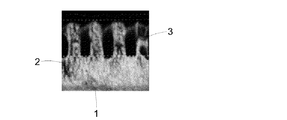
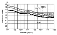
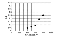
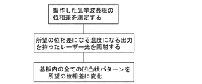
| Isano et al. | Improvement of phase retardation of wave plate with subwavelength structures by heat treatment | |
| CN117631111A (zh) | 一种基于离子注入的折射率调控光栅及制造方法 |
Legal Events
| Date | Code | Title | Description |
|---|---|---|---|
| A521 | Written amendment |
Free format text: JAPANESE INTERMEDIATE CODE: A523 Effective date: 20070222 |
|
| A621 | Written request for application examination |
Free format text: JAPANESE INTERMEDIATE CODE: A621 Effective date: 20070222 |
|
| A977 | Report on retrieval |
Free format text: JAPANESE INTERMEDIATE CODE: A971007 Effective date: 20091106 |
|
| A131 | Notification of reasons for refusal |
Free format text: JAPANESE INTERMEDIATE CODE: A131 Effective date: 20091110 |
|
| A521 | Written amendment |
Free format text: JAPANESE INTERMEDIATE CODE: A523 Effective date: 20091214 |
|
| TRDD | Decision of grant or rejection written | ||
| A01 | Written decision to grant a patent or to grant a registration (utility model) |
Free format text: JAPANESE INTERMEDIATE CODE: A01 Effective date: 20100112 |
|
| A01 | Written decision to grant a patent or to grant a registration (utility model) |
Free format text: JAPANESE INTERMEDIATE CODE: A01 |
|
| A61 | First payment of annual fees (during grant procedure) |
Free format text: JAPANESE INTERMEDIATE CODE: A61 Effective date: 20100114 |
|
| R150 | Certificate of patent or registration of utility model |
Free format text: JAPANESE INTERMEDIATE CODE: R150 |
|
| FPAY | Renewal fee payment (event date is renewal date of database) |
Free format text: PAYMENT UNTIL: 20130122 Year of fee payment: 3 |
|
| FPAY | Renewal fee payment (event date is renewal date of database) |
Free format text: PAYMENT UNTIL: 20140122 Year of fee payment: 4 |
|
| LAPS | Cancellation because of no payment of annual fees |