JP4261374B2 - 積層構造体及びその製造方法、並びに、超音波トランスデューサ - Google Patents
積層構造体及びその製造方法、並びに、超音波トランスデューサ Download PDFInfo
- Publication number
- JP4261374B2 JP4261374B2 JP2004003946A JP2004003946A JP4261374B2 JP 4261374 B2 JP4261374 B2 JP 4261374B2 JP 2004003946 A JP2004003946 A JP 2004003946A JP 2004003946 A JP2004003946 A JP 2004003946A JP 4261374 B2 JP4261374 B2 JP 4261374B2
- Authority
- JP
- Japan
- Prior art keywords
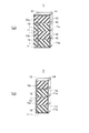
- substrate
- electrode layer
- layer
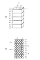
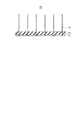
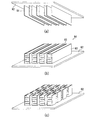
- columnar structures
- laminated structure
- Prior art date
- Legal status (The legal status is an assumption and is not a legal conclusion. Google has not performed a legal analysis and makes no representation as to the accuracy of the status listed.)
- Expired - Fee Related
Links
Images


Classifications
-
- B—PERFORMING OPERATIONS; TRANSPORTING
- B06—GENERATING OR TRANSMITTING MECHANICAL VIBRATIONS IN GENERAL
- B06B—METHODS OR APPARATUS FOR GENERATING OR TRANSMITTING MECHANICAL VIBRATIONS OF INFRASONIC, SONIC, OR ULTRASONIC FREQUENCY, e.g. FOR PERFORMING MECHANICAL WORK IN GENERAL
- B06B1/00—Methods or apparatus for generating mechanical vibrations of infrasonic, sonic, or ultrasonic frequency
- B06B1/02—Methods or apparatus for generating mechanical vibrations of infrasonic, sonic, or ultrasonic frequency making use of electrical energy
- B06B1/06—Methods or apparatus for generating mechanical vibrations of infrasonic, sonic, or ultrasonic frequency making use of electrical energy operating with piezoelectric effect or with electrostriction
- B06B1/0607—Methods or apparatus for generating mechanical vibrations of infrasonic, sonic, or ultrasonic frequency making use of electrical energy operating with piezoelectric effect or with electrostriction using multiple elements
- B06B1/0622—Methods or apparatus for generating mechanical vibrations of infrasonic, sonic, or ultrasonic frequency making use of electrical energy operating with piezoelectric effect or with electrostriction using multiple elements on one surface
- B06B1/064—Methods or apparatus for generating mechanical vibrations of infrasonic, sonic, or ultrasonic frequency making use of electrical energy operating with piezoelectric effect or with electrostriction using multiple elements on one surface with multiple active layers
-
- G—PHYSICS
- G01—MEASURING; TESTING
- G01N—INVESTIGATING OR ANALYSING MATERIALS BY DETERMINING THEIR CHEMICAL OR PHYSICAL PROPERTIES
- G01N29/00—Investigating or analysing materials by the use of ultrasonic, sonic or infrasonic waves; Visualisation of the interior of objects by transmitting ultrasonic or sonic waves through the object
- G01N29/22—Details, e.g. general constructional or apparatus details
- G01N29/24—Probes
- G01N29/2437—Piezoelectric probes
-
- G—PHYSICS
- G01—MEASURING; TESTING
- G01N—INVESTIGATING OR ANALYSING MATERIALS BY DETERMINING THEIR CHEMICAL OR PHYSICAL PROPERTIES
- G01N29/00—Investigating or analysing materials by the use of ultrasonic, sonic or infrasonic waves; Visualisation of the interior of objects by transmitting ultrasonic or sonic waves through the object
- G01N29/22—Details, e.g. general constructional or apparatus details
- G01N29/28—Details, e.g. general constructional or apparatus details providing acoustic coupling, e.g. water
-
- H—ELECTRICITY
- H10—SEMICONDUCTOR DEVICES; ELECTRIC SOLID-STATE DEVICES NOT OTHERWISE PROVIDED FOR
- H10N—ELECTRIC SOLID-STATE DEVICES NOT OTHERWISE PROVIDED FOR
- H10N30/00—Piezoelectric or electrostrictive devices
- H10N30/01—Manufacture or treatment
- H10N30/05—Manufacture of multilayered piezoelectric or electrostrictive devices, or parts thereof, e.g. by stacking piezoelectric bodies and electrodes
-
- H—ELECTRICITY
- H10—SEMICONDUCTOR DEVICES; ELECTRIC SOLID-STATE DEVICES NOT OTHERWISE PROVIDED FOR
- H10N—ELECTRIC SOLID-STATE DEVICES NOT OTHERWISE PROVIDED FOR
- H10N30/00—Piezoelectric or electrostrictive devices
- H10N30/01—Manufacture or treatment
- H10N30/07—Forming of piezoelectric or electrostrictive parts or bodies on an electrical element or another base
- H10N30/074—Forming of piezoelectric or electrostrictive parts or bodies on an electrical element or another base by depositing piezoelectric or electrostrictive layers, e.g. aerosol or screen printing
-
- H—ELECTRICITY
- H10—SEMICONDUCTOR DEVICES; ELECTRIC SOLID-STATE DEVICES NOT OTHERWISE PROVIDED FOR
- H10N—ELECTRIC SOLID-STATE DEVICES NOT OTHERWISE PROVIDED FOR
- H10N30/00—Piezoelectric or electrostrictive devices
- H10N30/50—Piezoelectric or electrostrictive devices having a stacked or multilayer structure
-
- H—ELECTRICITY
- H10—SEMICONDUCTOR DEVICES; ELECTRIC SOLID-STATE DEVICES NOT OTHERWISE PROVIDED FOR
- H10N—ELECTRIC SOLID-STATE DEVICES NOT OTHERWISE PROVIDED FOR
- H10N30/00—Piezoelectric or electrostrictive devices
- H10N30/80—Constructional details
- H10N30/87—Electrodes or interconnections, e.g. leads or terminals
- H10N30/872—Interconnections, e.g. connection electrodes of multilayer piezoelectric or electrostrictive devices
- H10N30/874—Interconnections, e.g. connection electrodes of multilayer piezoelectric or electrostrictive devices embedded within piezoelectric or electrostrictive material, e.g. via connections
-
- G—PHYSICS
- G01—MEASURING; TESTING
- G01N—INVESTIGATING OR ANALYSING MATERIALS BY DETERMINING THEIR CHEMICAL OR PHYSICAL PROPERTIES
- G01N2291/00—Indexing codes associated with group G01N29/00
- G01N2291/10—Number of transducers
- G01N2291/106—Number of transducers one or more transducer arrays
-
- Y—GENERAL TAGGING OF NEW TECHNOLOGICAL DEVELOPMENTS; GENERAL TAGGING OF CROSS-SECTIONAL TECHNOLOGIES SPANNING OVER SEVERAL SECTIONS OF THE IPC; TECHNICAL SUBJECTS COVERED BY FORMER USPC CROSS-REFERENCE ART COLLECTIONS [XRACs] AND DIGESTS
- Y10—TECHNICAL SUBJECTS COVERED BY FORMER USPC
- Y10T—TECHNICAL SUBJECTS COVERED BY FORMER US CLASSIFICATION
- Y10T29/00—Metal working
- Y10T29/42—Piezoelectric device making
-
- Y—GENERAL TAGGING OF NEW TECHNOLOGICAL DEVELOPMENTS; GENERAL TAGGING OF CROSS-SECTIONAL TECHNOLOGIES SPANNING OVER SEVERAL SECTIONS OF THE IPC; TECHNICAL SUBJECTS COVERED BY FORMER USPC CROSS-REFERENCE ART COLLECTIONS [XRACs] AND DIGESTS
- Y10—TECHNICAL SUBJECTS COVERED BY FORMER USPC
- Y10T—TECHNICAL SUBJECTS COVERED BY FORMER US CLASSIFICATION
- Y10T29/00—Metal working
- Y10T29/49—Method of mechanical manufacture
- Y10T29/49002—Electrical device making
- Y10T29/49005—Acoustic transducer
-
- Y—GENERAL TAGGING OF NEW TECHNOLOGICAL DEVELOPMENTS; GENERAL TAGGING OF CROSS-SECTIONAL TECHNOLOGIES SPANNING OVER SEVERAL SECTIONS OF THE IPC; TECHNICAL SUBJECTS COVERED BY FORMER USPC CROSS-REFERENCE ART COLLECTIONS [XRACs] AND DIGESTS
- Y10—TECHNICAL SUBJECTS COVERED BY FORMER USPC
- Y10T—TECHNICAL SUBJECTS COVERED BY FORMER US CLASSIFICATION
- Y10T428/00—Stock material or miscellaneous articles
- Y10T428/26—Web or sheet containing structurally defined element or component, the element or component having a specified physical dimension
- Y10T428/268—Monolayer with structurally defined element
-
- Y—GENERAL TAGGING OF NEW TECHNOLOGICAL DEVELOPMENTS; GENERAL TAGGING OF CROSS-SECTIONAL TECHNOLOGIES SPANNING OVER SEVERAL SECTIONS OF THE IPC; TECHNICAL SUBJECTS COVERED BY FORMER USPC CROSS-REFERENCE ART COLLECTIONS [XRACs] AND DIGESTS
- Y10—TECHNICAL SUBJECTS COVERED BY FORMER USPC
- Y10T—TECHNICAL SUBJECTS COVERED BY FORMER US CLASSIFICATION
- Y10T428/00—Stock material or miscellaneous articles
- Y10T428/31504—Composite [nonstructural laminate]
Landscapes
- Engineering & Computer Science (AREA)
- Manufacturing & Machinery (AREA)
- Analytical Chemistry (AREA)
- Pathology (AREA)
- Physics & Mathematics (AREA)
- Biochemistry (AREA)
- General Health & Medical Sciences (AREA)
- General Physics & Mathematics (AREA)
- Immunology (AREA)
- Chemical & Material Sciences (AREA)
- Life Sciences & Earth Sciences (AREA)
- Health & Medical Sciences (AREA)
- Mechanical Engineering (AREA)
- Ultra Sonic Daignosis Equipment (AREA)
- Investigating Or Analyzing Materials By The Use Of Ultrasonic Waves (AREA)
- Transducers For Ultrasonic Waves (AREA)
Priority Applications (2)
| Application Number | Priority Date | Filing Date | Title |
|---|---|---|---|
| JP2004003946A JP4261374B2 (ja) | 2004-01-09 | 2004-01-09 | 積層構造体及びその製造方法、並びに、超音波トランスデューサ |
| US11/030,069 US7199509B2 (en) | 2004-01-09 | 2005-01-07 | Multilayered structure and method of manufacturing the same, and ultrasonic transducer |
Applications Claiming Priority (1)
| Application Number | Priority Date | Filing Date | Title |
|---|---|---|---|
| JP2004003946A JP4261374B2 (ja) | 2004-01-09 | 2004-01-09 | 積層構造体及びその製造方法、並びに、超音波トランスデューサ |
Publications (3)
| Publication Number | Publication Date |
|---|---|
| JP2005198152A JP2005198152A (ja) | 2005-07-21 |
| JP2005198152A5 JP2005198152A5 (enExample) | 2006-07-13 |
| JP4261374B2 true JP4261374B2 (ja) | 2009-04-30 |
Family
ID=34818702
Family Applications (1)
| Application Number | Title | Priority Date | Filing Date |
|---|---|---|---|
| JP2004003946A Expired - Fee Related JP4261374B2 (ja) | 2004-01-09 | 2004-01-09 | 積層構造体及びその製造方法、並びに、超音波トランスデューサ |
Country Status (2)
| Country | Link |
|---|---|
| US (1) | US7199509B2 (enExample) |
| JP (1) | JP4261374B2 (enExample) |
Families Citing this family (11)
| Publication number | Priority date | Publication date | Assignee | Title |
|---|---|---|---|---|
| US7434305B2 (en) * | 2000-11-28 | 2008-10-14 | Knowles Electronics, Llc. | Method of manufacturing a microphone |
| US7378776B2 (en) * | 2005-09-06 | 2008-05-27 | Ariose Electronics Co. Ltd. | Piezoelectric ceramic composition and piezoelectric elements using the same |
| US7886801B2 (en) * | 2006-11-08 | 2011-02-15 | National Research Council Of Canada | Apparatus and process for stacking pieces of material |
| SG154342A1 (en) * | 2008-01-08 | 2009-08-28 | Opulent Electronics Internat P | Insulated metal substrate fabrication |
| US8286492B2 (en) * | 2009-12-09 | 2012-10-16 | The Boeing Company | Mode decomposition of sound waves using amplitude matching |
| US9166141B2 (en) * | 2011-09-09 | 2015-10-20 | Dvx, Llc | Process of manufacturing a piezopolymer transducer with matching layer |
| US9530955B2 (en) | 2011-11-18 | 2016-12-27 | Acist Medical Systems, Inc. | Ultrasound transducer and processing methods thereof |
| JP5874416B2 (ja) * | 2012-01-31 | 2016-03-02 | 三菱マテリアル株式会社 | ヒートシンク付パワーモジュール用基板の製造方法およびパワーモジュール用基板 |
| US9536511B2 (en) | 2013-12-31 | 2017-01-03 | Acist Medical Systems, Inc. | Ultrasound transducer stack |
| US9987809B2 (en) * | 2014-12-31 | 2018-06-05 | General Electric Company | System and method for manufacturing an ultrasound probe lens |
| US11333016B2 (en) | 2020-01-22 | 2022-05-17 | Halliburton Energy Services, Inc. | Ultrasonic transducer for measuring wellbore characteristics |
Family Cites Families (4)
| Publication number | Priority date | Publication date | Assignee | Title |
|---|---|---|---|---|
| US4803763A (en) * | 1986-08-28 | 1989-02-14 | Nippon Soken, Inc. | Method of making a laminated piezoelectric transducer |
| JP3352140B2 (ja) | 1993-03-31 | 2002-12-03 | オリンパス光学工業株式会社 | 誘電体積層部品とその製造方法 |
| JPH09261978A (ja) * | 1996-03-25 | 1997-10-03 | Nippon Cement Co Ltd | 積層体素子および振動駆動装置 |
| DE19757877A1 (de) * | 1997-12-24 | 1999-07-01 | Bosch Gmbh Robert | Verfahren zur Herstellung piezoelektrischer Aktoren und piezoelektrischer Aktor |
-
2004
- 2004-01-09 JP JP2004003946A patent/JP4261374B2/ja not_active Expired - Fee Related
-
2005
- 2005-01-07 US US11/030,069 patent/US7199509B2/en not_active Expired - Fee Related
Also Published As
| Publication number | Publication date |
|---|---|
| US7199509B2 (en) | 2007-04-03 |
| US20060154075A1 (en) | 2006-07-13 |
| JP2005198152A (ja) | 2005-07-21 |
Similar Documents
| Publication | Publication Date | Title |
|---|---|---|
| US7087970B2 (en) | Laminated structure, method of manufacturing the same and ultrasonic transducer array | |
| US7673385B2 (en) | Laminated structure method | |
| JP4261374B2 (ja) | 積層構造体及びその製造方法、並びに、超音波トランスデューサ | |
| US7765660B2 (en) | Method of manufacturing a multilayered piezoelectric element having internal electrodes and side electrodes | |
| US6964201B2 (en) | Large dimension, flexible piezoelectric ceramic tapes | |
| JP4601471B2 (ja) | 超音波トランスデューサアレイ及びその製造方法 | |
| JP7218134B2 (ja) | 静電容量型トランスデューサ、及びその製造方法 | |
| US20060067029A1 (en) | Multilayered structure, multilayered structure array and method of manufacturing the same | |
| JP4729260B2 (ja) | 積層構造体及びその製造方法 | |
| JP5289710B2 (ja) | 圧電素子及びインクジェットヘッド | |
| KR100676024B1 (ko) | 초음파 변환기 및 초음파 변환기의 제조 방법 | |
| JP2005317952A (ja) | 圧電アクチュエータ、インクジェットヘッド及びそれらの製造方法 | |
| JP4804760B2 (ja) | 積層型圧電構造体の製造方法 | |
| JP4094521B2 (ja) | 構造物の製造方法 | |
| JP2005117159A (ja) | 超音波トランスデューサアレイ及びその製造方法 | |
| JP5536310B2 (ja) | 積層型圧電素子及びその製造方法 | |
| JP4516327B2 (ja) | 積層構造体の製造方法 | |
| JP4238103B2 (ja) | 素子アレイの製造方法、及び、超音波トランスデューサアレイの製造方法 | |
| JP2004526345A (ja) | メタライゼーションが施されアブレーションされたポリマーフィルムを接地面として用いて、複数要素からなる音響プローブを製造する方法 | |
| JP2007095991A (ja) | 積層構造体及び積層構造体アレイ、並びに、それらの製造方法 | |
| JP2004120320A (ja) | 超音波トランスデューサアレイ及びその製造方法 | |
| JP3356820B2 (ja) | 超音波トランスデューサとその製造方法 | |
| JP2005102181A (ja) | 積層構造体及びその製造方法、並びに、超音波トランスデューサアレイ | |
| JP2004119934A (ja) | 積層構造体の製造方法及び製造装置 | |
| JP2026064933A (ja) | 波力発電装置 |
Legal Events
| Date | Code | Title | Description |
|---|---|---|---|
| A521 | Request for written amendment filed |
Free format text: JAPANESE INTERMEDIATE CODE: A523 Effective date: 20060530 |
|
| A621 | Written request for application examination |
Free format text: JAPANESE INTERMEDIATE CODE: A621 Effective date: 20060530 |
|
| A711 | Notification of change in applicant |
Free format text: JAPANESE INTERMEDIATE CODE: A712 Effective date: 20061205 |
|
| A977 | Report on retrieval |
Free format text: JAPANESE INTERMEDIATE CODE: A971007 Effective date: 20080925 |
|
| A131 | Notification of reasons for refusal |
Free format text: JAPANESE INTERMEDIATE CODE: A131 Effective date: 20081007 |
|
| A521 | Request for written amendment filed |
Free format text: JAPANESE INTERMEDIATE CODE: A523 Effective date: 20081111 |
|
| TRDD | Decision of grant or rejection written | ||
| A01 | Written decision to grant a patent or to grant a registration (utility model) |
Free format text: JAPANESE INTERMEDIATE CODE: A01 Effective date: 20090203 |
|
| A01 | Written decision to grant a patent or to grant a registration (utility model) |
Free format text: JAPANESE INTERMEDIATE CODE: A01 |
|
| A61 | First payment of annual fees (during grant procedure) |
Free format text: JAPANESE INTERMEDIATE CODE: A61 Effective date: 20090205 |
|
| FPAY | Renewal fee payment (event date is renewal date of database) |
Free format text: PAYMENT UNTIL: 20120220 Year of fee payment: 3 |
|
| R150 | Certificate of patent or registration of utility model |
Free format text: JAPANESE INTERMEDIATE CODE: R150 |
|
| LAPS | Cancellation because of no payment of annual fees |