JP4237442B2 - Transflective liquid crystal display device - Google Patents
Transflective liquid crystal display device Download PDFInfo
- Publication number
- JP4237442B2 JP4237442B2 JP2002055874A JP2002055874A JP4237442B2 JP 4237442 B2 JP4237442 B2 JP 4237442B2 JP 2002055874 A JP2002055874 A JP 2002055874A JP 2002055874 A JP2002055874 A JP 2002055874A JP 4237442 B2 JP4237442 B2 JP 4237442B2
- Authority
- JP
- Japan
- Prior art keywords
- substrate
- liquid crystal
- conductive film
- island
- display device
- Prior art date
- Legal status (The legal status is an assumption and is not a legal conclusion. Google has not performed a legal analysis and makes no representation as to the accuracy of the status listed.)
- Expired - Fee Related
Links
Images


Classifications
-
- G—PHYSICS
- G02—OPTICS
- G02F—OPTICAL DEVICES OR ARRANGEMENTS FOR THE CONTROL OF LIGHT BY MODIFICATION OF THE OPTICAL PROPERTIES OF THE MEDIA OF THE ELEMENTS INVOLVED THEREIN; NON-LINEAR OPTICS; FREQUENCY-CHANGING OF LIGHT; OPTICAL LOGIC ELEMENTS; OPTICAL ANALOGUE/DIGITAL CONVERTERS
- G02F1/00—Devices or arrangements for the control of the intensity, colour, phase, polarisation or direction of light arriving from an independent light source, e.g. switching, gating or modulating; Non-linear optics
- G02F1/01—Devices or arrangements for the control of the intensity, colour, phase, polarisation or direction of light arriving from an independent light source, e.g. switching, gating or modulating; Non-linear optics for the control of the intensity, phase, polarisation or colour
- G02F1/13—Devices or arrangements for the control of the intensity, colour, phase, polarisation or direction of light arriving from an independent light source, e.g. switching, gating or modulating; Non-linear optics for the control of the intensity, phase, polarisation or colour based on liquid crystals, e.g. single liquid crystal display cells
- G02F1/133—Constructional arrangements; Operation of liquid crystal cells; Circuit arrangements
- G02F1/1333—Constructional arrangements; Manufacturing methods
- G02F1/1343—Electrodes
- G02F1/13439—Electrodes characterised by their electrical, optical, physical properties; materials therefor; method of making
-
- G—PHYSICS
- G02—OPTICS
- G02F—OPTICAL DEVICES OR ARRANGEMENTS FOR THE CONTROL OF LIGHT BY MODIFICATION OF THE OPTICAL PROPERTIES OF THE MEDIA OF THE ELEMENTS INVOLVED THEREIN; NON-LINEAR OPTICS; FREQUENCY-CHANGING OF LIGHT; OPTICAL LOGIC ELEMENTS; OPTICAL ANALOGUE/DIGITAL CONVERTERS
- G02F1/00—Devices or arrangements for the control of the intensity, colour, phase, polarisation or direction of light arriving from an independent light source, e.g. switching, gating or modulating; Non-linear optics
- G02F1/01—Devices or arrangements for the control of the intensity, colour, phase, polarisation or direction of light arriving from an independent light source, e.g. switching, gating or modulating; Non-linear optics for the control of the intensity, phase, polarisation or colour
- G02F1/13—Devices or arrangements for the control of the intensity, colour, phase, polarisation or direction of light arriving from an independent light source, e.g. switching, gating or modulating; Non-linear optics for the control of the intensity, phase, polarisation or colour based on liquid crystals, e.g. single liquid crystal display cells
- G02F1/133—Constructional arrangements; Operation of liquid crystal cells; Circuit arrangements
- G02F1/1333—Constructional arrangements; Manufacturing methods
- G02F1/1335—Structural association of cells with optical devices, e.g. polarisers or reflectors
- G02F1/133553—Reflecting elements
- G02F1/133555—Transflectors
-
- G—PHYSICS
- G02—OPTICS
- G02F—OPTICAL DEVICES OR ARRANGEMENTS FOR THE CONTROL OF LIGHT BY MODIFICATION OF THE OPTICAL PROPERTIES OF THE MEDIA OF THE ELEMENTS INVOLVED THEREIN; NON-LINEAR OPTICS; FREQUENCY-CHANGING OF LIGHT; OPTICAL LOGIC ELEMENTS; OPTICAL ANALOGUE/DIGITAL CONVERTERS
- G02F1/00—Devices or arrangements for the control of the intensity, colour, phase, polarisation or direction of light arriving from an independent light source, e.g. switching, gating or modulating; Non-linear optics
- G02F1/01—Devices or arrangements for the control of the intensity, colour, phase, polarisation or direction of light arriving from an independent light source, e.g. switching, gating or modulating; Non-linear optics for the control of the intensity, phase, polarisation or colour
- G02F1/13—Devices or arrangements for the control of the intensity, colour, phase, polarisation or direction of light arriving from an independent light source, e.g. switching, gating or modulating; Non-linear optics for the control of the intensity, phase, polarisation or colour based on liquid crystals, e.g. single liquid crystal display cells
- G02F1/133—Constructional arrangements; Operation of liquid crystal cells; Circuit arrangements
- G02F1/1333—Constructional arrangements; Manufacturing methods
- G02F1/1335—Structural association of cells with optical devices, e.g. polarisers or reflectors
-
- G—PHYSICS
- G02—OPTICS
- G02F—OPTICAL DEVICES OR ARRANGEMENTS FOR THE CONTROL OF LIGHT BY MODIFICATION OF THE OPTICAL PROPERTIES OF THE MEDIA OF THE ELEMENTS INVOLVED THEREIN; NON-LINEAR OPTICS; FREQUENCY-CHANGING OF LIGHT; OPTICAL LOGIC ELEMENTS; OPTICAL ANALOGUE/DIGITAL CONVERTERS
- G02F1/00—Devices or arrangements for the control of the intensity, colour, phase, polarisation or direction of light arriving from an independent light source, e.g. switching, gating or modulating; Non-linear optics
- G02F1/01—Devices or arrangements for the control of the intensity, colour, phase, polarisation or direction of light arriving from an independent light source, e.g. switching, gating or modulating; Non-linear optics for the control of the intensity, phase, polarisation or colour
- G02F1/13—Devices or arrangements for the control of the intensity, colour, phase, polarisation or direction of light arriving from an independent light source, e.g. switching, gating or modulating; Non-linear optics for the control of the intensity, phase, polarisation or colour based on liquid crystals, e.g. single liquid crystal display cells
- G02F1/133—Constructional arrangements; Operation of liquid crystal cells; Circuit arrangements
- G02F1/1333—Constructional arrangements; Manufacturing methods
- G02F1/133345—Insulating layers
-
- G—PHYSICS
- G02—OPTICS
- G02F—OPTICAL DEVICES OR ARRANGEMENTS FOR THE CONTROL OF LIGHT BY MODIFICATION OF THE OPTICAL PROPERTIES OF THE MEDIA OF THE ELEMENTS INVOLVED THEREIN; NON-LINEAR OPTICS; FREQUENCY-CHANGING OF LIGHT; OPTICAL LOGIC ELEMENTS; OPTICAL ANALOGUE/DIGITAL CONVERTERS
- G02F1/00—Devices or arrangements for the control of the intensity, colour, phase, polarisation or direction of light arriving from an independent light source, e.g. switching, gating or modulating; Non-linear optics
- G02F1/01—Devices or arrangements for the control of the intensity, colour, phase, polarisation or direction of light arriving from an independent light source, e.g. switching, gating or modulating; Non-linear optics for the control of the intensity, phase, polarisation or colour
- G02F1/13—Devices or arrangements for the control of the intensity, colour, phase, polarisation or direction of light arriving from an independent light source, e.g. switching, gating or modulating; Non-linear optics for the control of the intensity, phase, polarisation or colour based on liquid crystals, e.g. single liquid crystal display cells
- G02F1/133—Constructional arrangements; Operation of liquid crystal cells; Circuit arrangements
- G02F1/1333—Constructional arrangements; Manufacturing methods
- G02F1/1335—Structural association of cells with optical devices, e.g. polarisers or reflectors
- G02F1/133509—Filters, e.g. light shielding masks
- G02F1/133514—Colour filters
-
- G—PHYSICS
- G02—OPTICS
- G02F—OPTICAL DEVICES OR ARRANGEMENTS FOR THE CONTROL OF LIGHT BY MODIFICATION OF THE OPTICAL PROPERTIES OF THE MEDIA OF THE ELEMENTS INVOLVED THEREIN; NON-LINEAR OPTICS; FREQUENCY-CHANGING OF LIGHT; OPTICAL LOGIC ELEMENTS; OPTICAL ANALOGUE/DIGITAL CONVERTERS
- G02F1/00—Devices or arrangements for the control of the intensity, colour, phase, polarisation or direction of light arriving from an independent light source, e.g. switching, gating or modulating; Non-linear optics
- G02F1/01—Devices or arrangements for the control of the intensity, colour, phase, polarisation or direction of light arriving from an independent light source, e.g. switching, gating or modulating; Non-linear optics for the control of the intensity, phase, polarisation or colour
- G02F1/13—Devices or arrangements for the control of the intensity, colour, phase, polarisation or direction of light arriving from an independent light source, e.g. switching, gating or modulating; Non-linear optics for the control of the intensity, phase, polarisation or colour based on liquid crystals, e.g. single liquid crystal display cells
- G02F1/133—Constructional arrangements; Operation of liquid crystal cells; Circuit arrangements
- G02F1/136—Liquid crystal cells structurally associated with a semi-conducting layer or substrate, e.g. cells forming part of an integrated circuit
- G02F1/1362—Active matrix addressed cells
- G02F1/136227—Through-hole connection of the pixel electrode to the active element through an insulation layer
-
- G—PHYSICS
- G02—OPTICS
- G02F—OPTICAL DEVICES OR ARRANGEMENTS FOR THE CONTROL OF LIGHT BY MODIFICATION OF THE OPTICAL PROPERTIES OF THE MEDIA OF THE ELEMENTS INVOLVED THEREIN; NON-LINEAR OPTICS; FREQUENCY-CHANGING OF LIGHT; OPTICAL LOGIC ELEMENTS; OPTICAL ANALOGUE/DIGITAL CONVERTERS
- G02F1/00—Devices or arrangements for the control of the intensity, colour, phase, polarisation or direction of light arriving from an independent light source, e.g. switching, gating or modulating; Non-linear optics
- G02F1/01—Devices or arrangements for the control of the intensity, colour, phase, polarisation or direction of light arriving from an independent light source, e.g. switching, gating or modulating; Non-linear optics for the control of the intensity, phase, polarisation or colour
- G02F1/13—Devices or arrangements for the control of the intensity, colour, phase, polarisation or direction of light arriving from an independent light source, e.g. switching, gating or modulating; Non-linear optics for the control of the intensity, phase, polarisation or colour based on liquid crystals, e.g. single liquid crystal display cells
- G02F1/133—Constructional arrangements; Operation of liquid crystal cells; Circuit arrangements
- G02F1/136—Liquid crystal cells structurally associated with a semi-conducting layer or substrate, e.g. cells forming part of an integrated circuit
- G02F1/1362—Active matrix addressed cells
- G02F1/136222—Colour filters incorporated in the active matrix substrate
Landscapes
- Physics & Mathematics (AREA)
- Nonlinear Science (AREA)
- Optics & Photonics (AREA)
- Crystallography & Structural Chemistry (AREA)
- Chemical & Material Sciences (AREA)
- General Physics & Mathematics (AREA)
- Mathematical Physics (AREA)
- Engineering & Computer Science (AREA)
- Microelectronics & Electronic Packaging (AREA)
- Liquid Crystal (AREA)
- Optical Elements Other Than Lenses (AREA)
- Optical Filters (AREA)
- Devices For Indicating Variable Information By Combining Individual Elements (AREA)
Description
【0001】
【発明の属する技術分野】
本発明は、パッシブマトリクス型、アクティブマトリクス型の液晶表示装置に関する。特に、透過型および反射型の両機能を兼ね備えた半透過型液晶表示装置の電極構造に関する。
【0002】
【従来の技術】
近年、携帯電話に代表される携帯情報端末の爆発的な普及により、軽量・省消費電力・使用環境の変化に応じて対応可能なディスプレイが必要とされている。
【0003】
なお、薄膜・軽量の面から考えると液晶表示装置、または有機EL表示装置が有望視されている代表格である。
【0004】
透過型表示装置は、ディスプレイを駆動させるためだけであれば、消費電力は少ない。しかし、液晶自体は発光しないので、ディスプレイとして表示を出すためにはバックライトを必要とする。携帯電話用途では、一般にELバックライトが用いられるが、このバックライトのために別途電力が必要となり、液晶特有の省消費電力の特徴が十分には活かせず、省消費電力化には不利である。また、暗い環境下ではディスプレイの表示がコントラスト良く見えるが、通常の明るい環境下では表示があまり良く見えなくなり、上方出射方式及び下方出射方式のいずれの場合においても使用環境に応じた適応性には難がある。
【0005】
また、有機EL表示装置は、表示素子自体が発光することが特徴である。消費電力は反射型液晶表示装置よりも大きくなるが、透過型液晶表示装置よりも(バックライト付き)よりも小さい。しかし、透過型液晶表示装置の場合と同じく、暗い環境下ではディスプレイの表示が良く見えるが、通常の明るい環境下では表示があまり良く見えないので、やはり、上方出射方式及び下方出射方式のいずれの場合においても使用環境に応じた適応性には難がある。
【0006】
さらに、反射型液晶表示装置は、表示のための光として環境中からの外光を利用する。ディスプレイ側からすると、基本的にはバックライトが不要であり、液晶と駆動回路を駆動させるための電力しか必要としないため、積極的な省消費電力化が図れる。しかし、前2者とは全く逆で、明るい環境下ではディスプレイの表示が良く見えるが、暗い環境下では表示があまり良く見えなくなる。携帯情報端末の用途を考えると、屋外の使用が主であり、比較的明るい環境で表示を見るケースが多いとはいえ、これでもやはり、使用環境に応じた適応性の点では不十分である。そのため、一部では、暗い環境下でも反射型表示装置として表示を行うことができるように、フロントライトを組み込んだものが市販されている。
【0007】
そこで、透過型と反射型液晶表示装置を組み合わせることにより、両者の利点を有する半透過型液晶ディスプレイが注目されている。明るい環境下では、反射型のもつ省消費電力とこの環境下での視認性の良さという特徴を活かし、一方暗い環境下では、バックライトを用いて、透過型の持つコントラストの良さという特徴を活かしている。
【0008】
半透過型の液晶表示装置としては、特開平11−101992号において開示されており、一つの表示画素に外光を反射する反射部とバックライトからの光を透過する透過部とを作り込むことにより、周囲が真っ暗の場合にはバックライトからの透過部を透過する光と反射率の比較的高い膜により形成した反射部により反射する光を利用して表示を行う両用型液晶表示装置として、さらに外光が明るい場合には、光反射率の比較的高い膜により形成した反射部により反射する光を利用して表示を行う反射型液晶表示装置として用いることができるというような構成の反射透過両用型(半透過型)の液晶表示装置である。
【0009】
また、上述した半透過型の液晶表示装置においては、特に反射表示を行う反射部において光拡散性を有する特殊な凹凸構造が付与されている。反射電極は、その構造上、表面に対して、ある方向からある入射角をもって入射した光に対して、ある特定の方向のある特定の出射角のところにしか反射しない(スネルの法則)ため、表面が平坦であると光の入射に対して光の出る方向、角度が一定に決まってしまうからである。このような状態でディスプレイを作製すると非常に視認性の悪い表示になる。
【0010】
さらに、透過型および反射型の液晶表示装置において、カラーフィルターの配置は、視差や画像のぼやけを生じる原因の一つとして挙げられる。
【0011】
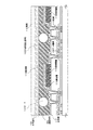
例えば、透過型の液晶表示において、図16(A)に示すように画素電極となる第1の電極(透明電極)1602を有する第1の基板(素子基板)1601と、対向電極となる第2の電極(透明電極)1606を有する第2の基板(対向基板)1603と、液晶層1607とを有し、第2の基板(対向基板)1603と第2の電極(透明電極)1606との間にはブラックマトリクス(BM)(1)1604およびカラーフィルター1605が形成される構造が一般的である。
【0012】
また、図16(A)に示すものよりも高解像度化を図る場合には、図16(B)に示すような構造にする場合もある。
【0013】
なお、透過型パネルにおいて、BMは通常液晶を駆動する際の配向乱れによって生じる光漏れを隠す目的でつけられる。BMやカラーフィルターを対向基板側に形成する場合には、液晶プロセスの中の張り合わせ工程において、素子基板と対向基板のそれぞれが、ある範囲内でずれることを予め想定してBMを少し大きく設定し、マージンとすることが普通である。
【0014】
従って、図16(B)に示すような高精細のパネルになると、このマージン(BMマージン(2))を確保するために開口部(開口部(2))が犠牲となるため深刻な開口率の低下につながることになる。
【0015】
そのため、これらの高解像度化に伴う開口率の低下を解決する方法としては、図16(C)に示すように第1の基板(素子基板)1621上にカラーフィルター1623を形成する方法が考えられている。
【0016】
図16(C)に示す場合においては、BM(3)に張り合わせ誤差に対するマージンを持たせる必要が無くなるため、開口率を犠牲にせずに開口部(3)を得ることができる。
【0017】
これに対して、反射型の液晶表示装置において、図17(A)に示すように画素電極となる第1の電極(反射電極)1702を有する第1の基板(素子基板)1701と、対向電極となる第2の電極(透明電極)1706を有する第2の基板(対向基板)1703と、液晶層1707とを有し、第2の基板(対向基板)1703と第2の電極(透明電極)1706との間にはブラックマトリクス(BM)(4)1704およびカラーフィルター1705が形成される構造が知られている。なお、この場合においては、第1の基板(素子基板)1701と第2の基板(対向基板)1703との張り合わせ誤差および光漏れを考慮したBMマージン(4)をとるため、開口部のサイズとしては、開口部(4)が得られる。
【0018】
この場合において、図17(A)に示すように光(1)は、入射光と出射光が同一の画素に形成されたカラーフィルターを透過するが、光(2)や、光(3)は、入射光と出射光が異なる画素に形成されたカラーフィルターを透過してしまう。つまり、カラーフィルターが対向基板側に形成される場合には、このように異なる画素に形成されたカラーフィルターを透過する割合が大きくなり、場合によっては、画像ぼけを生じるといった問題を有する。
【0019】
そのため、これらの画像ぼけの問題を解決する方法としては、図17(B)に示すように第1の基板(素子基板)1711上にカラーフィルター1714を形成する方法が考えられている。
【0020】
図17(B)に示す場合においては、BM(5)に張り合わせ誤差に対するマージンを持たせる必要が無くなるため開口率を犠牲にすることなく形成することができると共に、入射光と出射光が同一の画素に形成されたカラーフィルターを透過する割合が図17(A)に比べて高くなり、画像ぼけを防止することができるため好ましい方法である。
【0021】
しかし、この場合には、絶縁物である液晶層1717とカラーフィルター1714とが重なる構造を有し、カラーフィルターが画素容量の一部を形成するため、実効印加電圧の低下といった新たな問題を生じる。
【0022】
【発明が解決しようとする課題】
半透過型の液晶表示装置は、携帯情報端末という特殊な使用条件にうまく対応したディスプレイであるといえる。特に携帯電話用途では、今後も大きな需要が見込まれると予想される。そこで、安定した需要を確保するため、もしくは膨大な需要に対応するためには、より一層のコスト削減につとめる必要があることは明らかである。
【0023】
しかし、先に示したような凹凸構造を形成するためには、反射電極よりも下の層に凹凸形状を付けた後、その上に反射電極を形成する等の方法が必要となる。プロセスの中で、これを実現するためには、凹凸構造を形成するためのパターニングが必要となり、工程が増えることになる。工程が増えることは、歩留まりの低下や、プロセス時間の延長、コストの増加といった不利な事態を招くことになる。
【0024】
そこで、本発明では工程を特に増やすことなく形成された凹凸構造の反射電極を有する半透過型の液晶表示装置を提供することを目的とする。
【0025】
さらに、上述したような透過型および反射型液晶表示装置を作製する上で問題となるカラーフィルターの配置を半透過型液晶表示装置に最適なものとすることにより、視認性に優れた半透過型液晶表示装置を提供することを目的とする。
【0026】
【課題を解決するための手段】
上記課題を解決するために本発明では、半透過型の液晶表示装置を作製するにあたり、その製造プロセス中において、凹凸構造を形成するためだけのパターニング工程を特に増やすことなく、凹凸構造を形成することを特徴とする。
【0027】
さらに、本発明においては半透過型の液晶表示装置における視認性を向上させるためにカラーフィルターの配置を最適なものとするだけでなく、表示に影響を与えるような容量を増やすことなくカラーフィルターを設ける構造を形成することを特徴とする。
【0028】
本発明の液晶表示装置は、絶縁表面上に形成された複数の島状のパターンと、前記複数の島状のパターン上に形成されたカラーフィルターと、前記カラーフィルター上に形成された透明性導電膜と、を有することを特徴とする液晶表示装置である。
【0029】
なお、上記構成において前記複数の島状のパターンは、絶縁表面上に形成された反射性導電膜をエッチングすることにより形成することができる。さらに、前記複数の島状のパターンは反射性導電膜により形成されるため、入射した光を反射する機能を有する。
【0030】
また、本発明においてカラーフィルターが、複数の島状のパターンと、透明性導電膜からなる透明電極との間に挟まれて形成されることにより、複数の島状のパターンによる反射表示の場合においても、透明電極による表示の場合においても、従来の図00に示す液晶表示に比べ、カラーフィルターを通る光が所望の画素から表示される際の位置ずれを防ぐことができる。
【0031】
なお、本発明の半透過型液晶表示装置において、複数の島状のパターンと透明電極とがカラーフィルターを介して重なる位置に形成されている場合には、複数の島状のパターンにより光が反射され、透明電極とカラーフィルターを介して重なる位置に複数の島状のパターンが形成されていない場合には、光は透明電極を透過する。
【0032】
以上のことから、本発明の構造は、反射性と透過性という2種類の性質を有するだけでなく、反射性を有する部分に凹凸構造を形成することができる。
【0033】
また、本発明における反射性導電膜としては、波長400〜800nm(可視光領域)における垂直反射特性で75%以上の反射率をもつ導電膜を用いることとする。
【0034】
また、本発明の他の構成における液晶表示装置は、基板上に形成された薄膜トランジスタと、前記薄膜トランジスタ上に絶縁膜を介して形成された反射性導電膜をエッチングすることにより形成された配線および複数の島状のパターンと、前記複数の島状のパターン上に形成されたカラーフィルターと、前記カラーフィルター上に形成された透明性導電膜と、を有し、前記配線は、前記薄膜トランジスタおよび前記透明性導電膜を電気的に接続することを特徴とする液晶表示装置である。
【0035】
上記各構成において、反射性導電膜からなる島状のパターンと配線とがエッチングにより同時に形成される場合には、反射性導電膜からなる島状のパターンと配線とを同時に形成することができるため、通常凹凸構造を形成する際に用いられるフォトリソグラフィーの工程を減らすことができ、大幅なコスト削減と、生産性の向上を実現することができる。
【0036】
なお、複数の島状のパターンはランダムな形状、ランダムな配置で形成されている。但し、反射性導電膜をエッチングすることにより形成される島状のパターンは、反射の機能を向上させる上でパターン端部のテーパー角をより小さくすることが望ましい。
【0037】
さらに、画素部において、反射性導電膜からなる複数の島状のパターンが占める面積の割合は、画素部の面積の50〜90%であることを特徴とする。
【0038】
また、カラーフィルター上に形成される透明電極は、先に形成された配線と電気的に接続されるように形成される。
【0039】
さらに、本発明の液晶表示装置は、絶縁表面上に形成された反射性導電膜をエッチングすることにより形成された配線および複数の島状のパターンと、前記複数の島状のパターン上に形成されたカラーフィルターと、前記カラーフィルター上に形成された第1の透明性導電膜とを有する第1の基板と、第2の透明性導電膜を有する第2の基板と、液晶とを有し、前記第1の透明性導電膜および前記配線は、電気的に接続され、前記第1の基板の膜形成面と、前記第2の基板の膜形成面と、が互いに向き合って配置され、かつ前記第1の基板と、前記第2の基板と、の間に前記液晶が挟まれていることを特徴とする液晶表示装置である。
【0040】
さらに、本発明の液晶表示装置は、基板上に形成された薄膜トランジスタと、前記薄膜トランジスタ上に絶縁膜を介して形成された反射性導電膜をエッチングすることにより形成された配線および複数の島状のパターンと、前記複数の島状のパターン上に形成されたカラーフィルターと、前記カラーフィルター上に形成された第1の透明性導電膜とを有する第1の基板と、第2の透明性導電膜を有する第2の基板と、液晶とを有し、前記配線は、前記薄膜トランジスタと、前記第1の透明性導電膜とを電気的に接続し、前記第1の基板の膜形成面と、前記第2の基板の膜形成面と、が互いに向き合って配置され、かつ前記第1の基板と、前記第2の基板と、の間に前記液晶が挟まれていることを特徴とする液晶表示装置である。
【0041】
なお、本発明において、基板上に形成された反射性導電膜をエッチングすることにより形成された島状のパターン上にカラーフィルターを形成し、カラーフィルター上に透明性導電膜が形成された第1の基板と対向電極が形成された第2の基板とを膜形成面を内側にして、両基板の間に液晶を挟んで形成することにより、絶縁性材料からなるカラーフィルターと、液晶との間に透明電極が挟まれた構造を有するため、カラーフィルターによる容量の形成を低減させることができる。
【0042】
【発明の実施の形態】
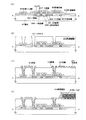
本発明の実施の態様を図1を参照して説明する。基板101上には半導体層105が形成されている。半導体層105は、非晶質半導体層を熱処理により結晶化させた多結晶半導体層で形成し、厚さは30〜750nm程度の厚さで形成する。さらにその上にはゲート絶縁膜106が形成されている。なお、ゲート絶縁膜106は30〜100nmの酸化シリコン膜により形成される。
【0043】
また、ゲート絶縁膜106上には、ゲート電極107、容量配線108が同一層で形成され、その上に酸化シリコン膜から成る第1絶縁膜109とアクリル膜から成る第2絶縁膜110が形成される。なお、第1絶縁膜109を形成する材料としては、酸化シリコン膜の他に、窒化シリコン膜、窒化酸化シリコン膜および塗布シリコン酸化膜(SOG:Spin On Glass)等のシリコンを含む無機材料を用いることができる。また、第2絶縁膜110を形成する材料としては、アクリル膜(感光性アクリルを含む)の他にポリイミド、ポリアミド、BCB(ベンゾシクロブテン)といった有機材料を用いることができる。
【0044】
配線112はTFT117のソース領域102とのコンタクトを形成する電極でもあり、ソース線でもある。また、配線113は、TFT117のドレイン領域103とのコンタクトを形成する電極である。
【0045】
半導体層105にはソース領域102、ドレイン領域103、およびチャネル形成領域104が形成されている。また、ソース領域102およびドレイン領域103を除き、容量配線108と重なる位置に形成される半導体層105は容量素子の一方の電極として機能している。
【0046】
また、配線112、113を形成する導電膜と同一の膜により、複数の島状のパターンである反射体114が形成される。なお、ここで形成される反射体114は、ランダムな形状、配置で形成される島状の構造を有することからその表面に入射された光を散乱させる機能を有する。
【0047】
なお、本発明において形成される反射体は、その形状を図2(A)で示すようにランダムな形状で、ランダムな位置に形成することにより、反射体204に対して入射される光の角度(入射角)と反射体により反射された光の角度(反射角)とをずらすことにより、光を散乱させることができる。
【0048】
なお、本発明において、入射角と反射角とをずらす上で重要となるのは、反射電極を構成する複数の反射体の形状であり、図2(B)に示す各反射体のテーパースロープ面(反射面)210が基板面(基準面)211に対してどの位傾いているかを示す角度であり、これをテーパー角(θ)212として示す。
【0049】
なお、本実施例では、このテーパー角(θ)212を5〜60°となるように反射体を形成することで基板面(基準面)211に対する出射角に比べてテーパースロープ面(反射面)210に対する出射角をずらして光を散乱させ、パネルの視認性を向上させることが可能である。
【0050】
図2(C)は、スロープのない反射面に対する入射光213、反射光214の挙動を示したものである。基準面211に対する入射方向をain、出射方向をaout、また反射面210に対する入射方向をa'in、出射方向をa'outとし、さらに入射角(φ1)215、出射角(φ2)216を基準面に対して定義することとすると、ここでは、基準面211と反射面210が一致していることから
ain=a'in=φ1、およびaout=a'out=φ2が成り立つ。
【0051】
また、スネルの法則により、a'in=a'outが成り立つことから、
ain=aout、およびφ1=φ2が成り立つ。
【0052】
一方、図2(D)は、テーパー角(θ)212がついたテーパースロープ面が反射面となっている場合の入射光213、出射光214の挙動を示したものである。
【0053】
入射光213および出射光214は、基準面211に対して、それぞれ入射角(φ1') 217、出射角(φ2')218とすると、
ain=φ1'、およびaout=φ2'であり、また、a'in=φ1'+θ、およびa'out=φ2'−θが成り立つ。
【0054】
また、スネルの法則により、a'in=a'outが成り立つことから、
φ1'+θ=φ2'−θが成り立つ。この式から、入射角(φ1') 217と出射角(φ2')218との関係をφ2'− φ1'=2θで示すことができる。これは、入射光213の入射方向(ain)と出射光214の出射方向(aout)とが2θずれていることを意味する。
【0055】
より視認性に優れたパネルを作製する上では、ここでのずれ角(2θ)を40°以下の範囲で均一に分布させることが好ましいことから、テーパー角(θ)212が20°以下となるように反射体204を形成することがさらに好ましい。
【0056】
本実施の形態においては、反射体204(図1の114)のテーパー角(θ)212を5〜60°で形成することにより、反射体204に入射した光を効率よく散乱させることができる。従って、本発明の構造は、TFTの作製プロセスを増加させることなく、ディスプレイの視認性を高めることが可能である。
【0057】
次に、図1に示すように反射体114上にカラーフィルター115が形成され、さらにカラーフィルター115上に透明電極116が形成される。なお、透明電極116は、入射した光を基板101側に透過させるための電極であり、透明電極116を形成する材料としては、酸化インジウム・スズ(ITO)膜や酸化インジウムに2〜20[%]の酸化亜鉛(ZnO)を混合した透明導電膜を用いて100〜200nmの膜厚で形成する。さらにこれをパターニングすることにより画素毎に透明電極116を形成する。
【0058】
本発明の構造によれば、透明電極116を透過して反射体114に入射した光は、反射体114の形状により散乱するが、反射体114に入射することなく反射体の隙間に入射した光は、基板101側に出射される。
【0059】
従って、本発明の構造は、TFTの作製プロセスを増加させることなく、光を散乱させるための反射体を形成することができるためディスプレイの視認性を高めることが可能である。さらに、透過型、反射型の液晶ディスプレイのいずれにおいても問題となるカラーフィルターの配置による位置ずれの問題を解決することができると共にカラーフィルターを設けることにより生じる容量の増加を防ぐことができる。
【0060】
なお、本実施の形態において説明した、基板上にTFTを有する素子基板(図1)に対向電極を有する対向基板(図示せず)を合わせ、両者の間に液晶を備えることにより半透過型の液晶表示装置を形成することができる。
【0061】
【実施例】
以下に、本発明の実施例について説明する。
【0062】
(実施例1)
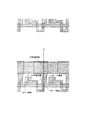
本実施例では、トップゲート型TFTを備えたアクティブマトリクス基板の作製工程の例を示す。なお、説明には画素部の一部の上面図および断面図を示した図3〜図7を用いる。
【0063】
まず、絶縁表面を有する基板301上に非晶質半導体層を形成する。ここでは基板301として石英基板を用い、非晶質半導体層を膜厚10〜100nmで形成する。
【0064】
なお、基板301には石英基板の他に、ガラス基板、プラスチック基板を用いることができる。ガラス基板を用いる場合には、ガラス歪み点よりも10〜20℃程度低い温度であらかじめ熱処理しておいても良い。また、基板301のTFTを形成する表面に、基板301からの不純物拡散を防ぐために、酸化シリコン膜、窒化シリコン膜または酸化窒化シリコン膜などの絶縁膜から成る下地膜を形成するとよい。
【0065】
非晶質半導体層として、膜厚60nmの非晶質シリコン膜(アモルファスシリコン膜)をLPCVD法により形成する。次いで、この非晶質半導体層を結晶化させる。ここでは、特開平8−78329号公報記載の技術を用いて結晶化させる。同公報記載の技術は、非晶質シリコン膜に対して結晶化を助長する金属元素を選択的に添加し、加熱処理を行うことで添加領域を起点として広がる結晶質シリコン膜を形成するものである。ここでは結晶化を助長する金属元素としてニッケルを用い、脱水素化のための熱処理(450℃、1時間)の後、結晶化のための熱処理(600℃、12時間)を行う。なお、ここでは、結晶化に上記公報記載の技術を用いたが特に限定されず、公知の結晶化処理(レーザー結晶化法、熱結晶化法等)を用いることが可能である。
【0066】
また、必要があれば、結晶化率を高め結晶粒内に残される欠陥を補修するためのレーザー光(XeCl:波長308nm)の照射を行う。レーザー光には波長400nm以下のエキシマレーザ光や、YAGレーザーの第2高調波、第3高調波を用いる。いずれにしても、繰り返し周波数10〜1000Hz程度のパルスレーザー光を用い、当該レーザー光を光学系にて100〜400mJ/cm2に集光し、90〜95%のオーバーラップ率をもって照射し、シリコン膜表面を走査させればよい。
【0067】
次いで、TFTの活性層とする領域からNiをゲッタリングする。ここでは、ゲッタリング方法として希ガス元素を含む半導体層を用いて行う例を示す。上記レーザー光の照射により形成された酸化膜に加え、オゾン水で表面を120秒処理して合計1〜5nmの酸化膜からなるバリア層を形成する。次いで、バリア層上にスパッタ法にてゲッタリングサイトとなるアルゴン元素を含む非晶質シリコン膜を膜厚150nmで形成する。本実施例のスパッタ法による成膜条件は、成膜圧力を0.3Paとし、ガス(Ar)流量を50(sccm)とし、成膜パワーを3kWとし、基板温度を150℃とする。なお、上記条件での非晶質シリコン膜に含まれるアルゴン元素の原子濃度は、3×10²⁰/cm3〜6×1020/cm3、酸素の原子濃度は1×1019/cm3〜3×1019/cm3である。その後、ランプアニール装置を用いて650℃、3分の熱処理を行いゲッタリングする。なお、ランプアニール装置の代わりに電気炉を用いてもよい。
【0068】
次いで、バリア層をエッチングストッパーとして、ゲッタリングサイトであるアルゴン元素を含む非晶質シリコン膜を選択的に除去した後、バリア層を希フッ酸で選択的に除去する。なお、ゲッタリングの際、ニッケルは酸素濃度の高い領域に移動しやすい傾向があるため、酸化膜からなるバリア層をゲッタリング後に除去することが望ましい。
【0069】
得られた結晶構造を有するシリコン膜(ポリシリコン膜とも呼ばれる)の表面にオゾン水で薄い酸化膜を形成した後、レジストからなるマスクを形成し、所望の形状にエッチング処理して島状に分離された半導体層305を形成する。半導体層305を形成した後、レジストからなるマスクを除去し、さらに半導体層305を覆うゲート絶縁膜306を100nmの膜厚で形成した後、熱酸化を行う。
【0070】
次いで、TFTのチャネル領域となる領域にp型またはn型の不純物元素を低濃度に添加するチャネルドープ工程を全面または選択的に行う。このチャネルドープ工程は、TFTのしきい値電圧を制御するための工程である。なお、半導体に対してp型を付与する不純物元素には、ボロン(B)、アルミニウム(Al)、ガリウム(Ga)など周期律第13族元素が知られている。また、半導体に対してn型を付与する不純物元素としては周期律15族に属する元素、典型的にはリン(P)または砒素(As)が知られている。なお、ここではジボラン(B2H6)を質量分離しないでプラズマ励起したイオンドープ法でボロンを添加する。もちろん、質量分離を行うイオンインプランテーション法を用いてもよい。
【0071】
次いで、第1の導電膜を形成し、パターニングを行ってゲート電極307および容量配線308を形成する。ここでは、窒化タンタル(TaN)(膜厚30nm)とタングステン(膜厚370nm)との積層構造を用いる。また、本実施例ではダブルゲート構造とする。なお、保持容量は、ゲート絶縁膜306を誘電体とし、容量配線308と半導体層305の一部である領域a(303a)とで構成されている。
【0072】
次いで、ゲート電極307および容量配線308をマスクとして自己整合的にリンを低濃度に添加する。この低濃度に添加された領域のリンの濃度が、1×10¹⁶〜5×10¹⁸/cm3、代表的には3×1017〜3×1018/cm3となるように調整する。
【0073】
次いで、マスク(図示せず)を形成してリンを高濃度に添加し、ソース領域302またはドレイン領域303となる高濃度不純物領域を形成する。この高濃度不純物領域のリンの濃度が1×10²⁰〜1×10²¹/cm3(代表的には2×1020〜5×1020/cm3)となるように調整する。なお、半導体層305のうち、ゲート電極307と重なる領域はチャネル形成領域304となり、マスクで覆われた領域は低濃度不純物領域となりLDD領域311となる。さらに、ゲート電極307、容量配線308、およびマスクのいずれにも覆われない領域は、ソース領域302、ドレイン領域303を含む高濃度不純物領域となる。
【0074】
なお、本実施例では同一基板上に画素部のTFTと駆動回路のTFTを形成するが、駆動回路のTFTにおいてもチャネル形成領域の両側であって、ソースおよびドレイン領域との間にソースおよびドレイン領域よりも不純物濃度の低い低濃度不純物領域を設けてもよいし、片側に低濃度不純物領域を設けてもよい。しかし、必ずしも両側に低濃度不純物領域を設ける必要はなく、実施者が適宜マスクを設計すればよい。
【0075】
次いで、ここでは図示しないが、画素と同一基板上に形成される駆動回路に用いるpチャネル型TFTを形成するために、マスクでnチャネル型TFTとなる領域を覆い、ボロンを添加してソース領域またはドレイン領域を形成する。
【0076】
次いで、マスクを除去した後、ゲート電極307および容量配線308を覆う第1絶縁膜309を形成する。ここでは、酸化シリコン膜を50nmの膜厚で形成し、半導体層305にそれぞれの濃度で添加されたn型またはp型不純物元素を活性化するための熱処理工程を行う。ここでは850℃、30分の加熱処理を行う(図3(A))。なお、ここでの画素上面図を図4に示す。図4において、点線A−A’で切断した断面図が図3(A)に相当する。
【0077】
次いで、水素化処理を行った後、有機樹脂材料からなる第2絶縁膜313を形成する。ここでは膜厚1μmのアクリル膜を用いることにより、第2絶縁膜313の表面を平坦化することができる。これにより、第2絶縁膜813の下層に形成されるパターンにより生じる段差の影響を防ぐことができる。次いで、第2絶縁膜313上にマスクを形成し、半導体層305に達するコンタクトホール312をエッチングにより形成する(図3(B))。そして、コンタクトホール312の形成後にマスクを除去する。なお、ここでの画素上面図を図5に示す。図5において、点線A−A’で切断した断面図が図3(B)に相当する。
【0078】
次に、第2の導電膜を形成し、これをパターニングすることにより反射体314の他、ソース線でもある配線315や、(ドレイン)配線316(具体的には、TFT310と、後で形成される透明電極とを電気的に接続する配線)を形成する。なお、ここで形成される第2の導電膜は、本発明における反射体を形成するための反射性導電膜であり、アルミニウム、銀等の他、これらを主成分とする合金材料を用いるのが好ましい。
【0079】
本実施例では、上記第2の導電膜としてTi膜を50nm、Siを含むアルミニウム膜500nmをスパッタ法で連続して形成した2層構造の積層膜を用いている。
【0080】
なお、パターニングの方法としてフォトリソグラフィーの技術を用い、複数の島状パターンからなる反射体314、および配線315、316を形成する。また、ここで用いるエッチング方法としては、ドライエッチング法を用い、テーパーエッチングおよび異方性エッチングを行う。
【0081】
はじめにレジストからなるマスクを形成して、テーパーエッチングを行うための第1のエッチング処理を行う。第1のエッチング処理では第1及び第2のエッチング条件で行う。エッチングにはICP(Inductively Coupled Plasma:誘導結合型プラズマ)エッチング法を用いると良い。ICPエッチング法を用い、エッチング条件(コイル型の電極に印加される電力量、基板側の電極に印加される電力量、基板側の電極温度等)を適宜調節することによって所望のテーパー形状に膜をエッチングすることができる。なお、エッチング用ガスとしては、Cl2、BCl3、SiCl4、CCl4などを代表とする塩素系ガスまたはCF4、SF6、NF3などを代表とするフッ素系ガス、またはO2を適宜用いることができる。
【0082】
本実施例では、第1のエッチング条件として、ICP(Inductively Coupled Plasma:誘導結合型プラズマ)エッチング法を用い、エッチング用ガスにBCl3とCl2とO2とを用い、それぞれのガス流量比を65/10/5(sccm)とし、1.2Paの圧力でコイル型の電極に500WのRF(13.56MHz)電力を投入してプラズマを生成してエッチングを行う。基板側(試料ステージ)にも300WのRF(13.56MHz)電力を投入し、実質的に負の自己バイアス電圧を印加する。この第1のエッチング条件によりSiを含むアルミニウム膜をエッチングして第1の導電層の端部をテーパー形状とする。
【0083】
この後、マスクを除去せずに第2のエッチング条件に変え、エッチング用ガスにCF4とCl2とO2とを用い、それぞれのガス流量比を25/25/10(sccm)とし、1Paの圧力でコイル型の電極に500WのRF(13.56MHz)電力を投入してプラズマを生成して約30秒程度のエッチングを行った。基板側(試料ステージ)にも20WのRF(13.56MHz)電力を投入し、実質的に負の自己バイアス電圧を印加する。CF4とCl2を混合した第2のエッチング条件では、Siを含むアルミニウム膜及びTi膜とも同程度にエッチングされる。
【0084】
こうして、第1のエッチング処理により第1の導電層と第2の導電層から成る第2の導電膜をテーパー形状とすることができる。
【0085】
次いで、レジストからなるマスクを除去せずに異方性エッチングを行うための第2のエッチング処理を行う。ここでは、エッチング用ガスにBCl3とCl2とを用い、それぞれのガス流量比を80/20(sccm)とし、1Paの圧力でコイル型の電極に300WのRF(13.56MHz)電力を投入してプラズマを生成してエッチングを行う。基板側(試料ステージ)にも50WのRF(13.56MHz)電力を投入し、実質的に負の自己バイアス電圧を印加する。
【0086】
以上により、反射体314、および配線315、316が形成されたところで、レジストを除去し、図3(C)に示す構造を得る。なお、ここでの画素上面図を図6に示す。図6において、点線A−A’で切断した断面図が図3(C)に相当する。
【0087】
次に、反射体314上にカラーフィルター317を形成する。カラーフィルター317の形成には、公知の材料を用いて行いることができる。本実施例では、これらの材料をスピンコート法により塗布し、1μmの膜厚で形成する。その後、ホットプレートにて80℃で5分間の予備硬化を行う。そして、フォトマスクを用いて、フォトリソグラフィー法により露光を行う。この処理が終わった基板は、現像液に浸し、揺動させることによって現像を行う。現像液は水酸化テトラメチルアンモニウムの0.2%水溶液を用いる。1分ほど現像液に浸したら、流水中で洗浄する。なお、高圧ジェット洗浄を行うことによりカラーフィルターの残渣を完全に取り去ることができる。なお、カラーフィルターの形成においては、対応する画素の有効開口部およびソース配線上に形成し、下層のTFTと、上層の画素電極とを電気的に接続する役割を果たすドレイン配線316上にはカラーフィルターが形成されないようにする。
【0088】
その後、パターンがきれいに形成されていることを確認できたら、クリーンオーブンにて250℃で1時間の本焼成を行う。ここでは、図示しないが本実施例では、以上の工程を赤、青、緑の3種のカラーフィルターについて行う。
【0089】
なお、3色のカラーフィルターが形成された後は、その上からオーバーコート材(図示せず)を塗布しても良い。
【0090】
次に、カラーフィルター317上に120nmの透明性導電膜(ここでは酸化インジウム・スズ(ITO)膜)をスパッタリング法により成膜し、これをフォトリソグラフィーの技術を用いて矩形にパターニングする。そして、ウエットエッチング処理を行った後で、クリーンオーブンにより250℃、60分の加熱処理を行うことにより、透明電極318を形成する(図3(D))。なお、ここでの画素上面図を図7に示す。図7において、点線A−A’で切断した断面図が図3(D)に相当する。
【0091】
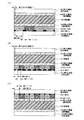
なお、図7に示すようにランダムに形成された反射体314上にカラーフィルター317を介して透明電極318を形成することにより、透明電極318と反射体314とが重なって形成されている部分においては、光は反射体314により反射され、反射体314が形成されない部分においては、光は反射体314により反射されることなく、基板301側へ出射する。
【0092】
以上の様にして、ダブルゲート構造を有するnチャネル型TFT、及び保持容量を有する画素部と、nチャネル型TFT及びpチャネル型TFTを有する駆動回路と、を同一基板上に形成することができる。本明細書中ではこのような基板を便宜上アクティブマトリクス基板と呼ぶ。
【0093】
なお、本実施例は一例であって本実施例の工程に限定されないことはいうまでもない。例えば、各導電膜としては、タンタル(Ta)、チタン(Ti)、モリブデン(Mo)、タングステン(W)、クロム(Cr)、シリコン(Si)から選ばれた元素、または元素を組み合わせた合金膜(代表的には、Mo―W合金、Mo―Ta合金)を用いることができる。また、各絶縁膜としては、酸化シリコン膜や窒化シリコン膜や酸化窒化シリコン膜や有機樹脂材料(ポリイミド、アクリル、ポリアミド、ポリイミドアミド、BCB(ベンゾシクロブテン)等)膜を用いることができる。
【0094】
また、本実施例で示す工程に従えば、図3(D)に示すように配線パターンマスクを用いて、反射体314、および配線(315、316)を同時に形成することができるため、アクティブマトリクス基板の作製に必要なフォトマスクの数を増やすことなく反射電極を透明電極上に島状に複数分離形成することができる。その結果、半透過型の液晶表示装置の作製において、工程を短縮し、製造コストの低減及び歩留まりの向上に寄与することができる。
【0095】
(実施例2)
本実施例では、実施例1とは構造の異なる半透過型の液晶表示装置の作製方法について図8〜図10を用いて詳細に説明する。
【0096】
まず、図8(A)に示すように基板801上に非晶質半導膜を形成し、これを結晶化した後、パターニングにより島状に分離された半導体層805を形成する。さらに、半導体層805上には、絶縁膜からなるゲート絶縁膜806が形成される。なお、ゲート絶縁膜806が形成されるまでの作製方法については、実施例1で示したのと同様であるので実施例1を参照すればよい。また、同様にして半導体層805を覆う絶縁膜を形成した後、熱酸化を行い、ゲート絶縁膜806を形成する。
【0097】
次いで、TFTのチャネル領域となる領域にp型またはn型の不純物元素を低濃度に添加するチャネルドープ工程を全面または選択的に行う。
【0098】
そして、ゲート絶縁膜806上に導電膜を形成し、これをパターニングすることによりゲート電極807、容量配線808、およびソース線となる配線809を形成することができる。なお、本実施例における第1の導電膜は50〜100nmの厚さに形成したTaN(窒化タンタル)と、100〜400nmの厚さに形成したW(タングステン)とを積層することにより形成する。
【0099】
なお、本実施例では、TaNとWとの積層膜を用いて導電膜を形成したが、特に限定されず、いずれもTa、W、Ti、Mo、Al、Cuから選ばれた元素、または前記元素を主成分とする合金材料若しくは化合物材料で形成してもよい。また、リン等の不純物元素をドーピングした多結晶シリコン膜に代表される半導体膜を用いてもよい。
【0100】
次に、ゲート電極807および容量配線808をマスクとして自己整合的にリンを低濃度に添加する。この低濃度に添加された領域のリンの濃度が、1×10¹⁶〜5×10¹⁸/cm3、代表的には3×1017〜3×1018/cm3となるように調整する。
【0101】
次いで、マスク(図示せず)を形成してリンを高濃度に添加し、ソース領域802またはドレイン領域803となる高濃度不純物領域を形成する。この高濃度不純物領域のリンの濃度が1×10²⁰〜1×10²¹/cm3(代表的には2×1020〜5×1020/cm3)となるように調整する。なお、半導体層805のうち、ゲート電極807と重なる領域はチャネル形成領域804となり、マスクで覆われた領域は低濃度不純物領域となりLDD領域811となる。さらに、ゲート電極807、容量配線808、およびマスクのいずれにも覆われない領域は、ソース領域802、ドレイン領域803を含む高濃度不純物領域となる。
【0102】
また、本実施例においても実施例1と同様にして、画素と同一基板上に形成される駆動回路に用いるpチャネル型TFTを形成するために、マスクでnチャネル型TFTとなる領域を覆い、ボロンを添加してソース領域またはドレイン領域を形成する。
【0103】
次いで、マスクを除去した後、ゲート電極807、容量配線808および配線(ソース線)809を覆う第1絶縁膜810を形成する。ここでは、酸化シリコン膜を50nmの膜厚で形成し、半導体層805にそれぞれの濃度で添加されたn型またはp型不純物元素を活性化するための熱処理工程を行う。ここでは850℃、30分の加熱処理を行う(図8(A))。なお、ここでの画素上面図を図9に示す。図9において、点線A−A’で切断した断面図が図8(A)に相当する。
【0104】
次いで、水素化処理を行った後、有機樹脂材料からなる第2絶縁膜813を形成する。ここでは膜厚1μmのアクリル膜を用いることにより、第2絶縁膜813の表面を平坦化することができる。これにより、第2絶縁膜813の下層に形成されるパターンにより生じる段差の影響を防ぐことができる。次いで、第2絶縁膜813上にマスクを形成し、半導体層805に達するコンタクトホール812をエッチングにより形成する(図8(B))。そして、コンタクトホール812の形成後にマスクを除去する。
【0105】
次に、第2の導電膜を形成し、これをパターニングすることにより、反射体814の他、配線(ソース線)809とTFT810のソース領域とを電気的に接続する配線815や、容量配線808と電気的に接続された配線816や、TFT810のドレイン領域と透明電極819とを電気的に接続する配線817(図8(D)では、その接続関係について図示されていない)を形成する。なお、ここで形成される第2の導電膜は、本発明における反射体を形成するための反射性導電膜であり、アルミニウム、銀の他、これらを主成分とする合金材料を用いるのが好ましい。
【0106】
本実施例では、上記第2の導電膜としてTi膜を50nm、Siを含むアルミニウム膜500nmをスパッタ法で連続して形成した2層構造の積層膜を用いている。
【0107】
なお、パターニングの方法としてフォトリソグラフィーの技術を用い、複数の島状パターンからなる反射体814、および配線815、816、817を形成する。また、ここで用いるエッチング方法としては、ドライエッチング法を用い、テーパーエッチングおよび異方性エッチングを行う。
【0108】
はじめにレジストからなるマスクを形成して、テーパーエッチングを行うための第1のエッチング処理を行う。第1のエッチング処理では第1及び第2のエッチング条件で行う。エッチングにはICP(Inductively Coupled Plasma:誘導結合型プラズマ)エッチング法を用いると良い。ICPエッチング法を用い、エッチング条件(コイル型の電極に印加される電力量、基板側の電極に印加される電力量、基板側の電極温度等)を適宜調節することによって所望のテーパー形状に膜をエッチングすることができる。なお、エッチング用ガスとしては、Cl2、BCl3、SiCl4、CCl4などを代表とする塩素系ガスまたはCF4、SF6、NF3などを代表とするフッ素系ガス、またはO2を適宜用いることができる。
【0109】
本実施例では、第1のエッチング条件として、ICP(Inductively Coupled Plasma:誘導結合型プラズマ)エッチング法を用い、エッチング用ガスにBCl3とCl2とO2とを用い、それぞれのガス流量比を65/10/5(sccm)とし、1.2Paの圧力でコイル型の電極に500WのRF(13.56MHz)電力を投入してプラズマを生成してエッチングを行う。基板側(試料ステージ)にも300WのRF(13.56MHz)電力を投入し、実質的に負の自己バイアス電圧を印加する。この第1のエッチング条件によりSiを含むアルミニウム膜をエッチングして第1の導電層の端部をテーパー形状とする。
【0110】
この後、マスクを除去せずに第2のエッチング条件に変え、エッチング用ガスにCF4とCl2とO2とを用い、それぞれのガス流量比を25/25/10(sccm)とし、1Paの圧力でコイル型の電極に500WのRF(13.56MHz)電力を投入してプラズマを生成して約30秒程度のエッチングを行った。基板側(試料ステージ)にも20WのRF(13.56MHz)電力を投入し、実質的に負の自己バイアス電圧を印加する。CF4とCl2を混合した第2のエッチング条件では、Siを含むアルミニウム膜及びTi膜とも同程度にエッチングされる。
【0111】
こうして、第1のエッチング処理により第1の導電層と第2の導電層から成る第2の導電膜をテーパー形状とすることができる。
【0112】
次いで、レジストからなるマスクを除去せずに異方性エッチングを行うための第2のエッチング処理を行う。ここでは、エッチング用ガスにBCl3とCl2とを用い、それぞれのガス流量比を80/20(sccm)とし、1Paの圧力でコイル型の電極に300WのRF(13.56MHz)電力を投入してプラズマを生成してエッチングを行う。基板側(試料ステージ)にも50WのRF(13.56MHz)電力を投入し、実質的に負の自己バイアス電圧を印加する。
【0113】
以上により、反射体814、および配線815、816、817が形成されたところで、レジストを除去し、図8(C)に示す構造を得る。なお、ここでの画素上面図を図9に示す。図9において、点線A−A’で切断した断面図が図8(C)に相当する。
【0114】
次に、反射体814上にカラーフィルター818を形成する。カラーフィルター818の形成には、公知の材料を用いて行いることができる。本実施例では、これらの材料をスピンコート法により塗布し、1μmの膜厚で形成する。その後、ホットプレートにて80℃で5分間の予備硬化を行う。そして、フォトマスクを用いて、フォトリソグラフィー法により露光を行う。この処理が終わった基板は、現像液に浸し、揺動させることによって現像を行う。現像液は水酸化テトラメチルアンモニウムの0.2%水溶液を用いる。1分ほど現像液に浸したら、流水中で洗浄する。なお、高圧ジェット洗浄を行うことによりカラーフィルターの残渣を完全に取り去ることができる。なお、カラーフィルターの形成においては、対応する画素の有効開口部のみに形成し、容量配線808と接続された配線816上にはカラーフィルターが形成されないようにする。また、配線817上の一部には、カラーフィルターが形成されるが、配線817と透明電極819とが接続される部分には形成されないようにする。
【0115】
その後、パターンがきれいに形成されていることを確認できたら、クリーンオーブンにて250℃で1時間の本焼成を行う。ここでは、図示しないが本実施例では、以上の工程を赤、青、緑の3種のカラーフィルターについて行う。
【0116】
なお、3色のカラーフィルターが形成された後は、その上からオーバーコート材(図示せず)を塗布しても良い。
【0117】
次に、カラーフィルター818上に120nmの透明性導電膜(ここでは酸化インジウム・スズ(ITO)膜)をスパッタリング法により成膜し、これをフォトリソグラフィーの技術を用いて矩形にパターニングする。そして、ウエットエッチング処理を行った後で、クリーンオーブンにより250℃、60分の加熱処理を行うことにより、透明電極813を形成する(図8(D))。なお、ここでの画素上面図を図10に示す。図10において、点線A−A’で切断した断面図が図8(D)に相当する。
【0118】
なお、図10に示すようにランダムに形成された反射体814上にカラーフィルター818を介して透明電極819を形成することにより、透明電極819と反射体814とが重なって形成されている部分においては、光は反射体814により反射され、反射体814が形成されない部分においては、光は反射体814により反射されることなく、基板801側へ出射する。
【0119】
以上の様にして、本実施例においてもダブルゲート構造を有するnチャネル型TFT、及び保持容量を有する画素部と、nチャネル型TFT及びpチャネル型TFTを有する駆動回路とが同一基板上に有するアクティブマトリクス基板が形成される。
【0120】
また、本実施例で示す工程に従えば、図8(D)に示すように配線パターンマスクを用いて、反射体814、および配線(815、816、817)を同時に形成することができるため、アクティブマトリクス基板の作製に必要なフォトマスクの数を増やすことなく反射体を島状に複数分離形成することができる。その結果、半透過型の液晶表示装置の作製において、工程を短縮し、製造コストの低減及び歩留まりの向上に寄与することができる。
【0121】
(実施例3)
本実施例では、実施例1で作製したアクティブマトリクス基板から、半透過型の液晶表示装置を作製する工程を以下に説明する。説明には図11の断面図を用いる。
【0122】
まず、実施例1に従い、図3(D)のアクティブマトリクス基板を得た後、図11に示すようにアクティブマトリクス基板上に配向膜1117を形成し、ラビング処理を行う。なお、本実施例では配向膜1117を形成する前に、基板間隔を保持するための球状のスペーサ1121を基板全面に散布した。また、球状のスペーサ1121に代えて、アクリル樹脂膜等の有機樹脂膜をパターニングすることによって柱状のスペーサを所望の位置に形成してもよい。
【0123】
次いで、基板1122を用意する。基板1122上に透明性導電膜からなる対向電極1123を画素部となる位置に形成し、基板1122の全面に配向膜1124を形成し、ラビング処理を施すことにより対向基板1126を得る。
【0124】
そして、その表面に配向膜1117が形成されたアクティブマトリクス基板と対向基板1126とをシール剤(図示せず)で貼り合わせる。シール剤にはフィラーが混入されていて、このフィラーと球状スペーサによって均一な間隔(好ましくは2.0〜3.0μm)を持って2枚の基板が貼り合わされる。その後、両基板の間に液晶材料1125を注入し、封止剤(図示せず)によって完全に封止する。液晶材料1125には公知の液晶材料を用いれば良い。このようにして図11に示す半透過型液晶表示装置が完成する。そして、必要があれば、アクティブマトリクス基板または対向基板1126を所望の形状に分断する。さらに、公知の技術を用いて偏光板等を適宜設けた。そして、公知の技術を用いてFPCを貼りつける。
【0125】
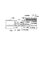
こうして得られた液晶モジュールの構成を図14の上面図を用いて説明する。アクティブマトリクス基板1401の中央には、画素部1404が配置されている。画素部1404の上側には、ソース信号線を駆動するためのソース信号線駆動回路1402が配置されている。画素部1404の左右には、ゲート信号線を駆動するためのゲート信号線駆動回路1403が配置されている。本実施例に示した例では、ゲート信号線駆動回路1403は画素部に対して左右対称配置としているが、これは片側のみの配置でも良く、液晶モジュールの基板サイズ等を考慮して、設計者が適宜選択すれば良い。ただし、回路の動作信頼性や駆動効率等を考えると、図14に示した左右対称配置が望ましい。
【0126】
各駆動回路への信号の入力は、フレキシブルプリント基板(Flexible Print Circuit:FPC)1405から行われる。FPC1405は、基板1401の所定の場所まで配置された配線に達するように、層間絶縁膜および樹脂膜にコンタクトホールを開口し、接続電極(図示せず)を形成した後、異方性導電膜等を介して圧着される。本実施例においては、接続電極はITOを用いて形成した。
【0127】
駆動回路、画素部の周辺には、基板外周に沿ってシール剤1407が塗布され、あらかじめアクティブマトリクス基板上に形成されたスペーサによって一定のギャップ(基板1401と対向基板1406との間隔)を保った状態で、対向基板806が貼り付けられる。その後、シール剤1407が塗布されていない部分より液晶素子が注入され、封止剤1408によって密閉される。以上の工程により、液晶モジュールが完成する。また、ここでは全ての駆動回路を基板上に形成した例を示したが、駆動回路の一部に数個のICを用いてもよい。以上のようにして、アクティブマトリクス型液晶表示装置が完成する。
【0128】
(実施例4)
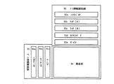
本発明を用いて作製された電気光学装置におけるブロック図を図12、13に示す。なお、図12には、アナログ駆動を行うための回路構成が示されている。本実施例は、ソース側駆動回路90、画素部91およびゲート側駆動回路92を有している電気光学装置について示している。なお、本明細書中において、駆動回路とはソース側処理回路およびゲート側駆動回路を含めた総称を指している。
【0129】
ソース側駆動回路90は、シフトレジスタ90a、バッファ90b、サンプリング回路(トランスファゲート)90cを設けている。また、ゲート側駆動回路92は、シフトレジスタ92a、レベルシフタ92b、バッファ92cを設けている。また、必要であればサンプリング回路とシフトレジスタとの間にレベルシフタ回路を設けてもよい。
【0130】
また、本実施例において、画素部91は複数の画素からなり、その複数の画素各々がTFT素子を含んでいる。
【0131】
なお、図示していないが、画素部91を挟んでゲート側駆動回路92の反対側にさらにゲート側駆動回路を設けても良い。
【0132】
また、デジタル駆動させる場合は、図13に示すように、サンプリング回路の代わりにラッチ(A)93b、ラッチ(B)93cを設ければよい。ソース側駆動回路93は、シフトレジスタ93a、ラッチ(A)93b、ラッチ(B)93c、D/Aコンバータ93d、バッファ93eを設けている。また、ゲート側駆動回路95は、シフトレジスタ95a、レベルシフタ95b、バッファ95cを設けている。また、必要であればラッチ(B)93cとD/Aコンバータ93dとの間にレベルシフタ回路を設けてもよい。
【0133】
なお、上記構成は、実施例1または実施例2に示した製造工程に従って実現することができる。また、本実施例では画素部と駆動回路の構成のみ示しているが、本発明の製造工程に従えば、メモリやマイクロプロセッサをも形成しうる。
【0134】
(実施例5)
本発明を実施して作製された半透過型の液晶表示装置は様々な電気光学装置に用いることができる。そして、そのような電気光学装置を表示媒体として組み込んだ電気器具全てに本発明を適用することができる。
【0135】
本発明により作製した液晶表示装置を用いて作製された電気器具として、ビデオカメラ、デジタルカメラ、ナビゲーションシステム、音響再生装置(カーオーディオ、オーディオコンポ等)、ノート型パーソナルコンピュータ、ゲーム機器、携帯情報端末(モバイルコンピュータ、携帯電話、携帯型ゲーム機または電子書籍等)、記録媒体を備えた画像再生装置(具体的にはデジタルビデオディスク(DVD)等の記録媒体を再生し、その画像を表示しうる表示装置を備えた装置)などが挙げられる。それら電気器具の具体例を図15に示す。
【0136】
図15(A)はデジタルスチルカメラであり、本体2101、表示部2102、受像部2103、操作キー2104、外部接続ポート2105、シャッター2106等を含む。本発明により作製した液晶表示装置をその表示部2102に用いることにより作製される。
【0137】
図15(B)はノート型パーソナルコンピュータであり、本体2201、筐体2202、表示部2203、キーボード2204、外部接続ポート2205、ポインティングマウス2206等を含む。本発明により作製した液晶表示装置をその表示部2203に用いることにより作製される。
【0138】
図15(C)はモバイルコンピュータであり、本体2301、表示部2302、スイッチ2303、操作キー2304、赤外線ポート2305等を含む。本発明により作製した液晶表示装置をその表示部2302に用いることにより作製される。
【0139】
図15(D)は記録媒体を備えた携帯型の画像再生装置(具体的にはDVD再生装置)であり、本体2401、筐体2402、表示部A2403、表示部B2404、記録媒体(DVD等)読み込み部2405、操作キー2406、スピーカー部2407等を含む。表示部A2403は主として画像情報を表示し、表示部B2404は主として文字情報を表示するが、本発明により作製した液晶表示装置をこれら表示部A、B2403、2404に用いることにより作製される。なお、記録媒体を備えた画像再生装置には家庭用ゲーム機器なども含まれる。
【0140】
図15(E)はビデオカメラであり、本体2601、表示部2602、筐体2603、外部接続ポート2604、リモコン受信部2605、受像部2606、バッテリー2607、音声入力部2608、操作キー2609、接眼部2610等を含む。本発明により作製した液晶表示装置をその表示部2602に用いることにより作製される。
【0141】
ここで図15(F)は携帯電話であり、本体2701、筐体2702、表示部2703、音声入力部2704、音声出力部2705、操作キー2706、外部接続ポート2707、アンテナ2708等を含む。本発明により作製した液晶表示装置をその表示部2703に用いることにより作製される。なお、表示部2703は黒色の背景に白色の文字を表示することで携帯電話の消費電力を抑えることができる。
【0142】
以上の様に、本発明において作製された液晶表示装置の適用範囲は極めて広く、あらゆる分野の電気器具を作製することが可能である。また、本実施の形態の電気器具は実施例1〜実施例4を実施することにより作製された液晶表示装置を用いることにより完成させることができる。
【0143】
【発明の効果】
以上により、本発明を実施することにより、半透過型の液晶表示装置の作製において、反射性導電膜からなる配線の形成と同時に反射体となる複数の島状パターンを同時に形成することができる。なお、本発明においては、反射体上にカラーフィルターを介して透明性導電膜からなる透明電極が形成されるため、作製行程を増やすことなく形成された反射体によりディスプレイの視認性を向上させることができるだけでなく、容量を増やすことなく画像のずれやぼやけを防ぐようにカラーフィルターを配置することができるため、大幅なコスト削減と、高品質な液晶表示装置の作製を実現することができる。
【図面の簡単な説明】
【図1】 本発明の液晶表示装置の素子構造を説明する図。
【図2】 本発明の反射体の構造を説明する図。
【図3】 本発明の液晶表示装置の作製工程を説明する図。
【図4】 本発明の液晶表示装置の作製工程を説明する図。
【図5】 本発明の液晶表示装置の作製工程を説明する図。
【図6】 本発明の液晶表示装置の作製工程を説明する図。
【図7】 本発明の液晶表示装置の作製工程を説明する図。
【図8】 本発明の液晶表示装置の作製工程を説明する図。
【図9】 本発明の液晶表示装置の作製工程を説明する図。
【図10】 本発明の液晶表示装置の作製工程を説明する図。
【図11】 本発明の液晶表示装置の構造を説明する図。
【図12】 本発明に用いることのできる回路構成を説明する図。
【図13】 本発明に用いることのできる回路構成を説明する図。
【図14】 本発明の液晶表示装置の外観を説明する図。
【図15】 電気器具の一例を示す図。
【図16】 従来技術について説明する図。
【図17】 従来技術について説明する図。
【符号の説明】
101 基板
102 ソース領域
103 ドレイン領域
104 チャネル形成領域
105 半導体層
106 ゲート絶縁膜
107 ゲート電極
108 容量配線
109 第1絶縁膜
110 第2絶縁膜
112、113 配線
114 反射体
115 カラーフィルター
116 透明電極[0001]
BACKGROUND OF THE INVENTION
The present invention relates to a passive matrix type and active matrix type liquid crystal display device. In particular, the present invention relates to an electrode structure of a transflective liquid crystal display device having both transmissive and reflective functions.
[0002]
[Prior art]
In recent years, with the explosive spread of portable information terminals typified by mobile phones, displays that can respond to changes in light weight, power saving, and usage environment are required.
[0003]
In terms of thin film and light weight, liquid crystal display devices or organic EL display devices are promising.
[0004]
The transmissive display device consumes less power only for driving the display. However, since the liquid crystal itself does not emit light, a backlight is required to display as a display. In the cellular phone application, an EL backlight is generally used. However, separate power is required for the backlight, and the characteristics of power saving peculiar to liquid crystals cannot be fully utilized, which is disadvantageous for power saving. . In addition, the display on the display looks good in a dark environment, but the display doesn't look very good in a normal bright environment, and the adaptability according to the operating environment is in either the upper emission method or the lower emission method. There are difficulties.
[0005]
The organic EL display device is characterized in that the display element itself emits light. The power consumption is larger than that of the reflective liquid crystal display device, but is smaller than that of the transmissive liquid crystal display device (with backlight). However, as in the case of the transmissive liquid crystal display device, the display on the display looks good in a dark environment, but the display does not look very good in a normal bright environment. Even in the case, there is a difficulty in adaptability according to the use environment.
[0006]
Further, the reflection type liquid crystal display device uses external light from the environment as light for display. From the display side, basically no backlight is required, and only power for driving the liquid crystal and the driving circuit is required, so that active power saving can be achieved. However, in contrast to the former two, the display on the display looks good in a bright environment, but the display does not look very good in a dark environment. Considering the use of portable information terminals, it is mainly used outdoors, and although there are many cases where the display is viewed in a relatively bright environment, this is still insufficient in terms of adaptability according to the usage environment. . Therefore, in some cases, a device incorporating a front light is commercially available so that display can be performed as a reflective display device even in a dark environment.
[0007]
Accordingly, attention has been paid to a transflective liquid crystal display having both advantages by combining a transmissive type and a reflective type liquid crystal display device. In a bright environment, we take advantage of the power-saving features of the reflective type and good visibility in this environment, while in a dark environment, we use a backlight to take advantage of the superior contrast characteristics of the transmissive type. ing.
[0008]
A transflective liquid crystal display device is disclosed in Japanese Patent Application Laid-Open No. 11-101992, and a reflective portion that reflects external light and a transmissive portion that transmits light from a backlight are formed in one display pixel. As a dual-use liquid crystal display device that performs display using light transmitted through the transmission part from the backlight and light reflected by the reflection part formed by a film having a relatively high reflectance when the surroundings are completely dark, Further, when the outside light is bright, it is possible to use as a reflection type liquid crystal display device that can be used as a reflection type liquid crystal display device that performs display using light reflected by a reflection portion formed by a film having a relatively high light reflectance. This is a dual-use (semi-transmissive) liquid crystal display device.
[0009]
Further, in the above-described transflective liquid crystal display device, a special concavo-convex structure having light diffusibility is provided particularly in a reflective portion that performs reflective display. Reflective electrodes reflect light incident on a surface at a certain incident angle from a certain direction only at a certain emission angle in a certain direction (Snell's law). This is because if the surface is flat, the direction and angle of light emission with respect to the incidence of light are fixed. When a display is manufactured in such a state, a display with very poor visibility is obtained.
[0010]
Further, in transmissive and reflective liquid crystal display devices, the arrangement of color filters is one of the causes of parallax and image blurring.
[0011]
For example, in a transmissive liquid crystal display, as shown in FIG. 16A, a first substrate (element substrate) 1601 having a first electrode (transparent electrode) 1602 serving as a pixel electrode and a second electrode serving as a counter electrode. A second substrate (counter substrate) 1603 having a second electrode (transparent electrode) 1606 and a liquid crystal layer 1607, and between the second substrate (counter substrate) 1603 and the second electrode (transparent electrode) 1606. In general, a black matrix (BM) (1) 1604 and a color filter 1605 are formed.
[0012]
Further, in the case of achieving higher resolution than that illustrated in FIG. 16A, a structure as illustrated in FIG.
[0013]
In a transmissive panel, BM is usually provided for the purpose of hiding light leakage caused by alignment disturbance when driving a liquid crystal. When the BM or color filter is formed on the counter substrate side, the BM is set to be slightly larger on the assumption that each of the element substrate and the counter substrate is shifted within a certain range in the bonding step in the liquid crystal process. It is common to use a margin.
[0014]
Therefore, in the case of a high-definition panel as shown in FIG. 16B, since the opening (opening (2)) is sacrificed in order to secure this margin (BM margin (2)), a serious opening ratio is obtained. Will lead to a decline.
[0015]
Therefore, as a method of solving the decrease in the aperture ratio accompanying the increase in resolution, a method of forming a color filter 1623 on the first substrate (element substrate) 1621 as shown in FIG. ing.
[0016]
In the case shown in FIG. 16C, the BM (3) does not need to have a margin for the bonding error, so that the opening (3) can be obtained without sacrificing the aperture ratio.
[0017]
On the other hand, in the reflective liquid crystal display device, as shown in FIG. 17A, a first substrate (element substrate) 1701 having a first electrode (reflective electrode) 1702 serving as a pixel electrode, and a counter electrode A second substrate (counter substrate) 1703 having a second electrode (transparent electrode) 1706, and a liquid crystal layer 1707, and the second substrate (counter substrate) 1703 and the second electrode (transparent electrode). A structure is known in which a black matrix (BM) (4) 1704 and a color filter 1705 are formed between the color filter 1705 and the color filter 1705. In this case, since the BM margin (4) in consideration of a bonding error between the first substrate (element substrate) 1701 and the second substrate (counter substrate) 1703 and light leakage is taken, the size of the opening is used. Opening (4) is obtained.
[0018]
In this case, as shown in FIG. 17A, the light (1) passes through a color filter in which incident light and outgoing light are formed in the same pixel, but the light (2) and the light (3) The incident light and the emitted light are transmitted through the color filter formed in different pixels. That is, when the color filter is formed on the counter substrate side, the ratio of transmitting through the color filter formed in different pixels in this way increases, and there is a problem that image blur may occur depending on the case.
[0019]
Therefore, as a method of solving these image blur problems, a method of forming a color filter 1714 on a first substrate (element substrate) 1711 as shown in FIG.
[0020]
In the case shown in FIG. 17B, it is not necessary to provide a margin for the bonding error in BM (5), so that it can be formed without sacrificing the aperture ratio, and the incident light and the emitted light are the same. This is a preferable method because the ratio of transmitting through the color filter formed in the pixel is higher than that in FIG. 17A and image blur can be prevented.
[0021]
However, in this case, the liquid crystal layer 1717 that is an insulator and the color filter 1714 overlap each other, and the color filter forms part of the pixel capacitance, which causes a new problem such as a decrease in effective applied voltage. .
[0022]
[Problems to be solved by the invention]
The transflective liquid crystal display device can be said to be a display that is well adapted to special usage conditions such as a portable information terminal. Especially for mobile phone applications, it is expected that there will be a great demand in the future. Therefore, it is clear that further cost reduction is necessary to ensure stable demand or to cope with enormous demand.
[0023]
However, in order to form the concavo-convex structure as described above, a method of forming a concavo-convex shape on a layer below the reflective electrode and then forming a reflective electrode thereon is necessary. In order to realize this in the process, patterning for forming the concavo-convex structure is necessary, and the number of processes is increased. An increase in the number of processes leads to disadvantageous situations such as a decrease in yield, an increase in process time, and an increase in cost.
[0024]
Therefore, an object of the present invention is to provide a transflective liquid crystal display device having a reflective electrode having a concavo-convex structure formed without particularly increasing the number of steps.
[0025]
Furthermore, by optimizing the arrangement of the color filter, which is a problem in manufacturing the transmission type and reflection type liquid crystal display devices as described above, for the semi-transmission type liquid crystal display device, the semi-transmission type having excellent visibility. An object is to provide a liquid crystal display device.
[0026]
[Means for Solving the Problems]
In order to solve the above-described problems, in the present invention, in manufacturing a transflective liquid crystal display device, a concavo-convex structure is formed without particularly increasing the number of patterning steps only for forming the concavo-convex structure during the manufacturing process. It is characterized by that.
[0027]
Further, in the present invention, not only the arrangement of the color filter is optimized in order to improve the visibility in the transflective liquid crystal display device, but the color filter is not increased without increasing the capacity that affects the display. The structure to provide is characterized by forming.
[0028]
The liquid crystal display device according to the present invention includes a plurality of island-shaped patterns formed on an insulating surface, a color filter formed on the plurality of island-shaped patterns, and a transparent conductive film formed on the color filter. A liquid crystal display device.
[0029]
Note that in the above structure, the plurality of island-shaped patterns can be formed by etching a reflective conductive film formed over an insulating surface. Furthermore, since the plurality of island-shaped patterns are formed of a reflective conductive film, they have a function of reflecting incident light.
[0030]
In the present invention, the color filter is formed by being sandwiched between a plurality of island-shaped patterns and a transparent electrode made of a transparent conductive film. Even in the case of display using a transparent electrode, it is possible to prevent positional deviation when light passing through the color filter is displayed from a desired pixel, as compared with the conventional liquid crystal display shown in FIG.
[0031]
In the transflective liquid crystal display device of the present invention, when a plurality of island-shaped patterns and transparent electrodes are formed at overlapping positions via a color filter, light is reflected by the plurality of island-shaped patterns. If a plurality of island-shaped patterns are not formed at positions overlapping the transparent electrode and the color filter, the light passes through the transparent electrode.
[0032]
From the above, the structure of the present invention has not only two kinds of properties, ie, reflectivity and transparency, but also can form a concavo-convex structure in a portion having reflectivity.
[0033]
In addition, as the reflective conductive film in the present invention, a conductive film having a reflectance of 75% or more in the vertical reflection characteristic at a wavelength of 400 to 800 nm (visible light region) is used.
[0034]
In addition, a liquid crystal display device according to another structure of the present invention includes a thin film transistor formed over a substrate, a wiring formed by etching a reflective conductive film formed over the thin film transistor via an insulating film, and a plurality of wirings. An island-shaped pattern, a color filter formed on the plurality of island-shaped patterns, and a transparent conductive film formed on the color filter, and the wiring includes the thin film transistor and the transparent A liquid crystal display device characterized in that a conductive film is electrically connected.
[0035]
In each of the above structures, when the island-shaped pattern and wiring made of the reflective conductive film are formed simultaneously by etching, the island-shaped pattern and wiring made of the reflective conductive film can be formed at the same time. Thus, the number of photolithography steps that are normally used for forming the concavo-convex structure can be reduced, and a significant cost reduction and an improvement in productivity can be realized.
[0036]
Note that the plurality of island-shaped patterns are formed in a random shape and a random arrangement. However, it is desirable that the island-shaped pattern formed by etching the reflective conductive film has a smaller taper angle at the end of the pattern in order to improve the reflection function.
[0037]
Further, the ratio of the area occupied by the plurality of island-shaped patterns made of the reflective conductive film in the pixel portion is 50 to 90% of the area of the pixel portion.
[0038]
The transparent electrode formed on the color filter is formed so as to be electrically connected to the previously formed wiring.
[0039]
Furthermore, the liquid crystal display device of the present invention is formed on the plurality of island-shaped patterns and the wiring and the plurality of island-shaped patterns formed by etching the reflective conductive film formed on the insulating surface. A first substrate having a color filter, a first transparent conductive film formed on the color filter, a second substrate having a second transparent conductive film, and a liquid crystal, The first transparent conductive film and the wiring are electrically connected, the film formation surface of the first substrate and the film formation surface of the second substrate are arranged to face each other, and the The liquid crystal display device is characterized in that the liquid crystal is sandwiched between a first substrate and the second substrate.
[0040]
Furthermore, the liquid crystal display device of the present invention includes a thin film transistor formed on a substrate, a wiring formed by etching a reflective conductive film formed on the thin film transistor via an insulating film, and a plurality of island-shaped electrodes. A first substrate having a pattern, a color filter formed on the plurality of island-shaped patterns, a first transparent conductive film formed on the color filter, and a second transparent conductive film A wiring board electrically connecting the thin film transistor and the first transparent conductive film, the film forming surface of the first substrate, and A liquid crystal display device, wherein a film forming surface of a second substrate is disposed to face each other, and the liquid crystal is sandwiched between the first substrate and the second substrate It is.
[0041]
In the present invention, the color filter is formed on the island-like pattern formed by etching the reflective conductive film formed on the substrate, and the transparent conductive film is formed on the color filter. The second substrate on which the counter electrode is formed and the second substrate on which the counter electrode is formed are formed such that the film forming surface is on the inside and the liquid crystal is sandwiched between the two substrates so that the color filter made of an insulating material is interposed between the liquid crystal and the liquid crystal. Since the transparent electrode is sandwiched between the electrodes, the formation of capacitance by the color filter can be reduced.
[0042]
DETAILED DESCRIPTION OF THE INVENTION
An embodiment of the present invention will be described with reference to FIG. A semiconductor layer 105 is formed on the substrate 101. The semiconductor layer 105 is formed of a polycrystalline semiconductor layer obtained by crystallizing an amorphous semiconductor layer by heat treatment, and has a thickness of about 30 to 750 nm. Furthermore, a gate insulating film 106 is formed thereon. Note that the gate insulating film 106 is formed of a silicon oxide film having a thickness of 30 to 100 nm.
[0043]
On the gate insulating film 106, a gate electrode 107 and a capacitor wiring 108 are formed in the same layer, and a first insulating film 109 made of a silicon oxide film and a second insulating film 110 made of an acrylic film are formed thereon. The As a material for forming the first insulating film 109, an inorganic material containing silicon such as a silicon nitride film, a silicon nitride oxide film, and a coated silicon oxide film (SOG: Spin On Glass) is used in addition to the silicon oxide film. be able to. In addition to the acrylic film (including photosensitive acrylic), an organic material such as polyimide, polyamide, or BCB (benzocyclobutene) can be used as the material for forming the second insulating film 110.
[0044]
The wiring 112 is also an electrode that forms a contact with the source region 102 of the TFT 117 and is also a source line. The wiring 113 is an electrode that forms a contact with the drain region 103 of the TFT 117.
[0045]
A source region 102, a drain region 103, and a channel formation region 104 are formed in the semiconductor layer 105. In addition, except for the source region 102 and the drain region 103, the semiconductor layer 105 formed in a position overlapping with the capacitor wiring 108 functions as one electrode of the capacitor.
[0046]
In addition, the reflector 114 which is a plurality of island-shaped patterns is formed using the same film as the conductive film forming the wirings 112 and 113. Note that the reflector 114 formed here has an island-like structure formed with a random shape and arrangement, and thus has a function of scattering light incident on the surface thereof.
[0047]
Note that the reflector formed in the present invention has a random shape as shown in FIG. 2A and is formed at random positions, whereby the angle of light incident on the reflector 204 is formed. The light can be scattered by shifting the (incident angle) and the angle of the light reflected by the reflector (reflection angle).
[0048]
In the present invention, what is important in shifting the incident angle and the reflection angle is the shape of the plurality of reflectors constituting the reflection electrode, and the tapered slope surface of each reflector shown in FIG. This is an angle indicating how much the (reflecting surface) 210 is inclined with respect to the substrate surface (reference surface) 211, and this is indicated as a taper angle (θ) 212.
[0049]
In this embodiment, the reflector is formed so that the taper angle (θ) 212 is 5 to 60 °, so that the taper slope surface (reflective surface) is larger than the emission angle with respect to the substrate surface (reference surface) 211. It is possible to shift the emission angle with respect to 210 to scatter light and improve the visibility of the panel.
[0050]
FIG. 2C shows the behavior of incident light 213 and reflected light 214 with respect to a reflecting surface having no slope. The incident direction with respect to the
a in = A ' in = Φ 1 And a out = A ' out = Φ 2 Holds.
[0051]
Also, according to Snell's law, a ' in = A ' out Because
a in = A out , And φ 1 = Φ 2 Holds.
[0052]
On the other hand, FIG. 2D shows the behavior of the incident light 213 and the
[0053]
The incident light 213 and the
a in = Φ 1 ', And a out = Φ 2 'And also a' in = Φ 1 '+ Θ and a' out = Φ 2 '−θ holds.
[0054]
Also, according to Snell's law, a ' in = A ' out Because
φ 1 '+ Θ = φ 2 '−θ holds. From this equation, the incident angle (φ 1 ') 217 and exit angle (φ 2 ') The relationship with 218 is φ 2 '−φ 1 It can be shown by '= 2θ. This is because the incident direction of incident light 213 (a in ) And the outgoing direction of the outgoing light 214 (a out ) Is shifted by 2θ.
[0055]
In producing a panel with higher visibility, it is preferable to uniformly distribute the deviation angle (2θ) in the range of 40 ° or less, and therefore the taper angle (θ) 212 is 20 ° or less. More preferably, the reflector 204 is formed.
[0056]
In this embodiment, the light incident on the reflector 204 can be efficiently scattered by forming the taper angle (θ) 212 of the reflector 204 (114 in FIG. 1) at 5 to 60 °. Therefore, the structure of the present invention can improve the visibility of the display without increasing the TFT manufacturing process.
[0057]
Next, as shown in FIG. 1, the color filter 115 is formed on the reflector 114, and the transparent electrode 116 is further formed on the color filter 115. Note that the transparent electrode 116 is an electrode for transmitting incident light to the substrate 101 side. As a material for forming the transparent electrode 116, 2 to 20% of an indium tin oxide (ITO) film or indium oxide is used. The film is formed to a thickness of 100 to 200 nm using a transparent conductive film mixed with zinc oxide (ZnO). Furthermore, the transparent electrode 116 is formed for every pixel by patterning this.
[0058]
According to the structure of the present invention, the light that has passed through the transparent electrode 116 and entered the reflector 114 is scattered by the shape of the reflector 114, but is incident on the gap between the reflectors without entering the reflector 114. Is emitted to the substrate 101 side.
[0059]
Therefore, the structure of the present invention can increase the visibility of a display because a reflector for scattering light can be formed without increasing the TFT manufacturing process. Further, it is possible to solve the problem of misalignment due to the arrangement of the color filter, which is a problem in both the transmissive type and the reflective type liquid crystal display, and to prevent an increase in capacity caused by providing the color filter.
[0060]
Note that a transflective type is obtained by combining a counter substrate (not shown) having a counter electrode with an element substrate (FIG. 1) having a TFT on a substrate described in this embodiment and providing a liquid crystal therebetween. A liquid crystal display device can be formed.
[0061]
【Example】
Examples of the present invention will be described below.
[0062]
Example 1
In this embodiment, an example of a manufacturing process of an active matrix substrate including a top gate type TFT is shown. For description, FIGS. 3 to 7 showing a top view and a cross-sectional view of a part of the pixel portion are used.
[0063]
First, an amorphous semiconductor layer is formed over the substrate 301 having an insulating surface. Here, a quartz substrate is used as the substrate 301, and an amorphous semiconductor layer is formed with a thickness of 10 to 100 nm.
[0064]
Note that the substrate 301 can be a glass substrate or a plastic substrate in addition to a quartz substrate. When a glass substrate is used, heat treatment may be performed in advance at a temperature lower by about 10 to 20 ° C. than the glass strain point. In order to prevent impurity diffusion from the substrate 301, a base film made of an insulating film such as a silicon oxide film, a silicon nitride film, or a silicon oxynitride film is preferably formed on the surface of the substrate 301 on which the TFT is formed.
[0065]
As the amorphous semiconductor layer, an amorphous silicon film (amorphous silicon film) having a thickness of 60 nm is formed by LPCVD. Next, this amorphous semiconductor layer is crystallized. Here, crystallization is performed using the technique described in JP-A-8-78329. The technique described in this publication is to selectively add a metal element that promotes crystallization to an amorphous silicon film and perform a heat treatment to form a crystalline silicon film that spreads from the added region as a starting point. is there. Here, nickel is used as a metal element for promoting crystallization, and after heat treatment for dehydrogenation (450 ° C., 1 hour), heat treatment for crystallization (600 ° C., 12 hours) is performed. Here, the technique described in the above publication is used for crystallization, but is not particularly limited, and a known crystallization process (laser crystallization method, thermal crystallization method, or the like) can be used.
[0066]
If necessary, irradiation with a laser beam (XeCl: wavelength 308 nm) for increasing the crystallization rate and repairing defects left in the crystal grains is performed. As the laser light, excimer laser light having a wavelength of 400 nm or less, and second harmonic and third harmonic of a YAG laser are used. In any case, pulse laser light having a repetition frequency of about 10 to 1000 Hz is used, and the laser light is 100 to 400 mJ / cm in the optical system. 2 And the surface of the silicon film may be scanned by irradiating with an overlap rate of 90 to 95%.
[0067]
Next, Ni is gettered from the region used as the active layer of the TFT. Here, an example is shown in which a gettering method is performed using a semiconductor layer containing a rare gas element. In addition to the oxide film formed by the laser light irradiation, the surface is treated with ozone water for 120 seconds to form a barrier layer made of an oxide film having a total thickness of 1 to 5 nm. Next, an amorphous silicon film containing an argon element serving as a gettering site is formed with a thickness of 150 nm on the barrier layer by a sputtering method. The film formation conditions by the sputtering method of this embodiment are as follows: the film formation pressure is 0.3 Pa, the gas (Ar) flow rate is 50 (sccm), the film formation power is 3 kW, and the substrate temperature is 150 ° C. Note that the atomic concentration of the argon element contained in the amorphous silicon film under the above conditions is 3 × 10 20 /cm Three ~ 6 × 10 20 /cm Three The atomic concentration of oxygen is 1 × 10 19 /cm Three ~ 3x10 19 /cm Three It is. Thereafter, heat treatment is performed at 650 ° C. for 3 minutes using a lamp annealing apparatus to perform gettering. An electric furnace may be used instead of the lamp annealing apparatus.
[0068]
Next, the amorphous silicon film containing an argon element as a gettering site is selectively removed using the barrier layer as an etching stopper, and then the barrier layer is selectively removed with dilute hydrofluoric acid. Note that during gettering, nickel tends to move to a region with a high oxygen concentration, and thus it is desirable to remove the barrier layer made of an oxide film after gettering.
[0069]
After forming a thin oxide film with ozone water on the surface of the obtained silicon film having a crystal structure (also called a polysilicon film), a resist mask is formed, etched into a desired shape, and separated into islands The formed semiconductor layer 305 is formed. After the semiconductor layer 305 is formed, the resist mask is removed, and a gate insulating film 306 covering the semiconductor layer 305 is formed to a thickness of 100 nm, and then thermal oxidation is performed.
[0070]
Next, a channel doping process in which a p-type or n-type impurity element is added at a low concentration in a region to be a channel region of the TFT is performed over the entire surface or selectively. This channel doping process is a process for controlling the threshold voltage of the TFT. As impurity elements imparting p-type to a semiconductor, periodic group 13 elements such as boron (B), aluminum (Al), and gallium (Ga) are known. As an impurity element imparting n-type to a semiconductor, an element belonging to Group 15 of the periodic table, typically phosphorus (P) or arsenic (As) is known. Here, diborane (B 2 H 6 Boron is added by ion doping that is plasma-excited without mass separation. Of course, an ion implantation method that performs mass separation may be used.
[0071]
Next, a first conductive film is formed and patterned to form the gate electrode 307 and the capacitor wiring 308. Here, a stacked structure of tantalum nitride (TaN) (film thickness: 30 nm) and tungsten (film thickness: 370 nm) is used. In this embodiment, a double gate structure is used. Note that the storage capacitor includes the capacitor wiring 308 and a region a (303a) which is part of the semiconductor layer 305 using the gate insulating film 306 as a dielectric.
[0072]
Next, phosphorus is added at a low concentration in a self-aligning manner using the gate electrode 307 and the capacitor wiring 308 as a mask. The concentration of phosphorus in this low concentration region is 1 × 10 16 ~ 5x10 18 /cm Three , Typically 3 × 10 17 ~ 3x10 18 /cm Three Adjust so that
[0073]
Next, a mask (not shown) is formed and phosphorus is added at a high concentration, so that a high concentration impurity region which becomes the source region 302 or the drain region 303 is formed. The phosphorus concentration in this high concentration impurity region is 1 × 10 20 ~ 1x10 twenty one /cm Three (Typically 2 × 10 20 ~ 5x10 20 /cm Three ). Note that a region of the semiconductor layer 305 that overlaps with the gate electrode 307 serves as a channel formation region 304, and a region covered with the mask serves as a low concentration impurity region and serves as an LDD region 311. Further, a region that is not covered by any of the gate electrode 307, the capacitor wiring 308, and the mask is a high concentration impurity region including the source region 302 and the drain region 303.
[0074]
In this embodiment, the TFT of the pixel portion and the TFT of the driving circuit are formed on the same substrate, but the TFT of the driving circuit is also on both sides of the channel formation region and between the source and drain regions. A low concentration impurity region having an impurity concentration lower than that of the region may be provided, or a low concentration impurity region may be provided on one side. However, it is not always necessary to provide low-concentration impurity regions on both sides, and a practitioner may design a mask appropriately.
[0075]
Next, although not shown here, in order to form a p-channel TFT used for a driver circuit formed over the same substrate as the pixel, a region that becomes an n-channel TFT is covered with a mask, and boron is added to form a source region. Alternatively, a drain region is formed.
[0076]
Next, after removing the mask, a first insulating film 309 covering the gate electrode 307 and the capacitor wiring 308 is formed. Here, a silicon oxide film is formed to a thickness of 50 nm, and a heat treatment step for activating the n-type or p-type impurity element added to the semiconductor layer 305 at each concentration is performed. Here, heat treatment is performed at 850 ° C. for 30 minutes (FIG. 3A). A top view of the pixel here is shown in FIG. In FIG. 4, a cross-sectional view taken along the dotted line AA ′ corresponds to FIG.
[0077]
Next, after performing hydrogenation treatment, a second insulating film 313 made of an organic resin material is formed. Here, the surface of the second insulating film 313 can be planarized by using an acrylic film with a thickness of 1 μm. Thereby, it is possible to prevent the influence of the step caused by the pattern formed under the second insulating film 813. Next, a mask is formed over the second insulating film 313, and a contact hole 312 reaching the semiconductor layer 305 is formed by etching (FIG. 3B). Then, the mask is removed after the contact hole 312 is formed. A top view of the pixel here is shown in FIG. In FIG. 5, a cross-sectional view taken along the dotted line AA ′ corresponds to FIG.
[0078]
Next, a second conductive film is formed and patterned to form a
[0079]
In this embodiment, a multilayer film having a two-layer structure in which a Ti film of 50 nm and an Si-containing aluminum film of 500 nm are continuously formed by a sputtering method is used as the second conductive film.
[0080]
Note that a photolithography technique is used as a patterning method, and a
[0081]
First, a mask made of resist is formed, and a first etching process for performing taper etching is performed. The first etching process is performed under the first and second etching conditions. For etching, an ICP (Inductively Coupled Plasma) etching method may be used. Using the ICP etching method, the film is formed into a desired taper shape by appropriately adjusting the etching conditions (the amount of power applied to the coil-type electrode, the amount of power applied to the substrate-side electrode, the electrode temperature on the substrate side, etc.) Can be etched. As an etching gas, Cl 2 , BCl Three , SiCl Four , CCl Four Chlorine gas or CF represented by Four , SF 6 , NF Three Fluorine gas such as O 2 Can be used as appropriate.
[0082]
In this embodiment, an ICP (Inductively Coupled Plasma) etching method is used as the first etching condition, and BCl is used as an etching gas. Three And Cl 2 And O 2 The gas flow ratio is 65/10/5 (sccm), and 500 W of RF (13.56 MHz) power is applied to the coil-type electrode at a pressure of 1.2 Pa to generate plasma and etch. I do. 300 W RF (13.56 MHz) power is also applied to the substrate side (sample stage), and a substantially negative self-bias voltage is applied. The aluminum film containing Si is etched under the first etching condition so that the end portion of the first conductive layer is tapered.
[0083]
After that, the second etching condition is changed without removing the mask, and the etching gas is changed to CF. Four And Cl 2 And O 2 Each gas flow rate ratio is 25/25/10 (sccm), and 500 W of RF (13.56 MHz) power is applied to the coil electrode at a pressure of 1 Pa to generate plasma for about 30 seconds. About etching was performed. 20 W RF (13.56 MHz) power is also applied to the substrate side (sample stage), and a substantially negative self-bias voltage is applied. CF Four And Cl 2 Under the second etching condition in which is mixed, both the aluminum film containing Si and the Ti film are etched to the same extent.
[0084]
Thus, the second conductive film including the first conductive layer and the second conductive layer can be tapered by the first etching process.
[0085]
Next, a second etching process is performed to perform anisotropic etching without removing the resist mask. Here, BCl is used as an etching gas. Three And Cl 2 The gas flow ratio is 80/20 (sccm) and 300 W RF (13.56 MHz) power is applied to the coil-type electrode at a pressure of 1 Pa to generate plasma and perform etching. 50 W RF (13.56 MHz) power is also applied to the substrate side (sample stage), and a substantially negative self-bias voltage is applied.
[0086]
As described above, when the
[0087]
Next, a
[0088]
Thereafter, when it is confirmed that the pattern is formed cleanly, main baking is performed at 250 ° C. for 1 hour in a clean oven. Here, although not shown, in the present embodiment, the above process is performed for three types of color filters of red, blue, and green.
[0089]
Note that after the three color filters are formed, an overcoat material (not shown) may be applied thereon.
[0090]
Next, a 120 nm transparent conductive film (here, indium tin oxide (ITO) film) is formed on the
[0091]
As shown in FIG. 7, the transparent electrode 318 is formed on the
[0092]
As described above, an n-channel TFT having a double gate structure, a pixel portion having a storage capacitor, and a driver circuit having an n-channel TFT and a p-channel TFT can be formed over the same substrate. . In this specification, such a substrate is referred to as an active matrix substrate for convenience.
[0093]
Needless to say, the present embodiment is an example and is not limited to the steps of the present embodiment. For example, as each conductive film, an element film selected from tantalum (Ta), titanium (Ti), molybdenum (Mo), tungsten (W), chromium (Cr), and silicon (Si), or an alloy film in which elements are combined (Typically, a Mo—W alloy or a Mo—Ta alloy) can be used. As each insulating film, a silicon oxide film, a silicon nitride film, a silicon oxynitride film, or an organic resin material (polyimide, acrylic, polyamide, polyimide amide, BCB (benzocyclobutene), or the like) film can be used.
[0094]
Further, according to the steps shown in this embodiment, the
[0095]
(Example 2)
In this embodiment, a method for manufacturing a transflective liquid crystal display device having a structure different from that of
[0096]
First, as shown in FIG. 8A, an amorphous semiconductor film is formed over a substrate 801, crystallized, and then a semiconductor layer 805 separated into islands by patterning is formed. Further, a gate insulating film 806 made of an insulating film is formed over the semiconductor layer 805. Note that since a manufacturing method until the gate insulating film 806 is formed is similar to that described in
[0097]
Next, a channel doping process in which a p-type or n-type impurity element is added at a low concentration in a region to be a channel region of the TFT is performed over the entire surface or selectively.
[0098]
Then, by forming a conductive film over the gate insulating film 806 and patterning the conductive film, a gate electrode 807, a capacitor wiring 808, and a wiring 809 to be a source line can be formed. Note that the first conductive film in this embodiment is formed by stacking TaN (tantalum nitride) formed to a thickness of 50 to 100 nm and W (tungsten) formed to a thickness of 100 to 400 nm.
[0099]
In this example, the conductive film was formed using a stacked film of TaN and W, but there is no particular limitation, and any of the elements selected from Ta, W, Ti, Mo, Al, Cu, or the above You may form with the alloy material or compound material which has an element as a main component. Alternatively, a semiconductor film typified by a polycrystalline silicon film doped with an impurity element such as phosphorus may be used.
[0100]
Next, phosphorus is added at a low concentration in a self-aligning manner using the gate electrode 807 and the capacitor wiring 808 as a mask. The concentration of phosphorus in this low concentration region is 1 × 10 16 ~ 5x10 18 /cm Three , Typically 3 × 10 17 ~ 3x10 18 /cm Three Adjust so that
[0101]
Next, a mask (not shown) is formed and phosphorus is added at a high concentration, so that a high concentration impurity region which becomes the source region 802 or the drain region 803 is formed. The phosphorus concentration in this high concentration impurity region is 1 × 10 20 ~ 1x10 twenty one /cm Three (Typically 2 × 10 20 ~ 5x10 20 /cm Three ). Note that a region of the semiconductor layer 805 that overlaps with the gate electrode 807 serves as a channel formation region 804, and a region covered with the mask serves as a low-concentration impurity region and serves as an
[0102]
Also in this embodiment, in the same manner as in
[0103]
Next, after removing the mask, a first insulating film 810 that covers the gate electrode 807, the capacitor wiring 808, and the wiring (source line) 809 is formed. Here, a silicon oxide film is formed to a thickness of 50 nm, and a heat treatment step for activating the n-type or p-type impurity element added to the semiconductor layer 805 at each concentration is performed. Here, heat treatment is performed at 850 ° C. for 30 minutes (FIG. 8A). A top view of the pixel here is shown in FIG. In FIG. 9, a cross-sectional view taken along the dotted line AA ′ corresponds to FIG.
[0104]
Next, after performing hydrogenation treatment, a second insulating film 813 made of an organic resin material is formed. Here, the surface of the second insulating film 813 can be planarized by using an acrylic film with a thickness of 1 μm. Thereby, it is possible to prevent the influence of the step caused by the pattern formed under the second insulating film 813. Next, a mask is formed over the second insulating film 813, and a contact hole 812 reaching the semiconductor layer 805 is formed by etching (FIG. 8B). Then, the mask is removed after the contact hole 812 is formed.
[0105]
Next, by forming a second conductive film and patterning it, in addition to the
[0106]
In this embodiment, a multilayer film having a two-layer structure in which a Ti film of 50 nm and an Si-containing aluminum film of 500 nm are continuously formed by a sputtering method is used as the second conductive film.
[0107]
Note that a photolithography technique is used as a patterning method, and a
[0108]
First, a mask made of resist is formed, and a first etching process for performing taper etching is performed. The first etching process is performed under the first and second etching conditions. For etching, an ICP (Inductively Coupled Plasma) etching method may be used. Using the ICP etching method, the film is formed into a desired taper shape by appropriately adjusting the etching conditions (the amount of power applied to the coil-type electrode, the amount of power applied to the substrate-side electrode, the electrode temperature on the substrate side, etc.) Can be etched. As an etching gas, Cl 2 , BCl Three , SiCl Four , CCl Four Chlorine gas or CF represented by Four , SF 6 , NF Three Fluorine gas such as O 2 Can be used as appropriate.
[0109]
In this embodiment, an ICP (Inductively Coupled Plasma) etching method is used as the first etching condition, and BCl is used as an etching gas. Three And Cl 2 And O 2 The gas flow ratio is 65/10/5 (sccm), and 500 W of RF (13.56 MHz) power is applied to the coil-type electrode at a pressure of 1.2 Pa to generate plasma and etch. I do. 300 W RF (13.56 MHz) power is also applied to the substrate side (sample stage), and a substantially negative self-bias voltage is applied. The aluminum film containing Si is etched under the first etching condition so that the end portion of the first conductive layer is tapered.
[0110]
After that, the second etching condition is changed without removing the mask, and the etching gas is changed to CF. Four And Cl 2 And O 2 Each gas flow rate ratio is 25/25/10 (sccm), and 500 W of RF (13.56 MHz) power is applied to the coil electrode at a pressure of 1 Pa to generate plasma for about 30 seconds. About etching was performed. 20 W RF (13.56 MHz) power is also applied to the substrate side (sample stage), and a substantially negative self-bias voltage is applied. CF Four And Cl 2 Under the second etching condition in which is mixed, both the aluminum film containing Si and the Ti film are etched to the same extent.
[0111]
Thus, the second conductive film including the first conductive layer and the second conductive layer can be tapered by the first etching process.
[0112]
Next, a second etching process is performed to perform anisotropic etching without removing the resist mask. Here, BCl is used as an etching gas. Three And Cl 2 The gas flow ratio is 80/20 (sccm) and 300 W RF (13.56 MHz) power is applied to the coil-type electrode at a pressure of 1 Pa to generate plasma and perform etching. 50 W RF (13.56 MHz) power is also applied to the substrate side (sample stage), and a substantially negative self-bias voltage is applied.
[0113]
As described above, when the
[0114]
Next, a
[0115]
Thereafter, when it is confirmed that the pattern is formed cleanly, main baking is performed at 250 ° C. for 1 hour in a clean oven. Here, although not shown, in the present embodiment, the above process is performed for three types of color filters of red, blue, and green.
[0116]
Note that after the three color filters are formed, an overcoat material (not shown) may be applied thereon.
[0117]
Next, a 120 nm transparent conductive film (here, indium tin oxide (ITO) film) is formed on the
[0118]
As shown in FIG. 10, the transparent electrode 819 is formed on the randomly formed
[0119]
As described above, also in this embodiment, the n-channel TFT having the double gate structure, the pixel portion having the storage capacitor, and the driving circuit having the n-channel TFT and the p-channel TFT are provided on the same substrate. An active matrix substrate is formed.
[0120]
Further, according to the steps shown in this embodiment, the
[0121]
(Example 3)
In this embodiment, a process for manufacturing a transflective liquid crystal display device from the active matrix substrate manufactured in
[0122]
First, after obtaining the active matrix substrate of FIG. 3D in accordance with
[0123]
Next, a substrate 1122 is prepared. A counter electrode 1123 made of a transparent conductive film is formed over the substrate 1122 at a position to be a pixel portion, an alignment film 1124 is formed over the entire surface of the substrate 1122, and a counter substrate 1126 is obtained by performing a rubbing process.
[0124]
Then, the active matrix substrate on which the
[0125]
The structure of the liquid crystal module thus obtained will be described with reference to the top view of FIG. A pixel portion 1404 is arranged in the center of the active matrix substrate 1401. A source signal line driver circuit 1402 for driving the source signal line is disposed above the pixel portion 1404. On the left and right sides of the pixel portion 1404, gate signal
[0126]
Input of signals to each drive circuit is performed from a flexible printed circuit (FPC) 1405. The FPC 1405 opens a contact hole in the interlayer insulating film and the resin film so as to reach the wiring arranged up to a predetermined place on the substrate 1401, and after forming a connection electrode (not shown), an anisotropic conductive film or the like It is crimped through. In this example, the connection electrode was formed using ITO.
[0127]
A sealant 1407 is applied around the periphery of the driving circuit and the pixel portion along the outer periphery of the substrate, and a predetermined gap (a space between the substrate 1401 and the counter substrate 1406) is maintained by a spacer formed on the active matrix substrate in advance. In this state, the counter substrate 806 is attached. Thereafter, a liquid crystal element is injected from a portion where the sealant 1407 is not applied and is sealed with the sealant 1408. The liquid crystal module is completed through the above steps. Although an example in which all the drive circuits are formed on the substrate is shown here, several ICs may be used as part of the drive circuit. As described above, an active matrix liquid crystal display device is completed.
[0128]
(Example 4)
Block diagrams of electro-optical devices manufactured using the present invention are shown in FIGS. FIG. 12 shows a circuit configuration for performing analog driving. In this embodiment, an electro-optical device having a source side driver circuit 90, a pixel portion 91, and a gate
[0129]
The source side driver circuit 90 includes a shift register 90a, a buffer 90b, and a sampling circuit (transfer gate) 90c. The gate
[0130]
In this embodiment, the pixel unit 91 includes a plurality of pixels, and each of the plurality of pixels includes a TFT element.
[0131]
Although not shown, a gate side drive circuit may be further provided on the opposite side of the gate
[0132]
In the case of digital driving, a latch (A) 93b and a latch (B) 93c may be provided instead of the sampling circuit as shown in FIG. The source
[0133]
In addition, the said structure is realizable according to the manufacturing process shown in Example 1 or Example 2. FIG. In this embodiment, only the configuration of the pixel portion and the drive circuit is shown. However, according to the manufacturing process of the present invention, a memory and a microprocessor can be formed.
[0134]
(Example 5)
The transflective liquid crystal display device manufactured by implementing the present invention can be used for various electro-optical devices. The present invention can be applied to all electric appliances incorporating such an electro-optical device as a display medium.
[0135]
As an electric appliance manufactured using the liquid crystal display device manufactured according to the present invention, a video camera, a digital camera, a navigation system, a sound reproduction device (car audio, audio component, etc.), a notebook personal computer, a game machine, a portable information terminal (Mobile computer, mobile phone, portable game machine, electronic book, or the like), an image playback device equipped with a recording medium (specifically, a recording medium such as a digital video disc (DVD) can be played back and the image can be displayed. And a device provided with a display device). Specific examples of these electric appliances are shown in FIG.
[0136]
FIG. 15A illustrates a digital still camera, which includes a
[0137]
FIG. 15B shows a laptop personal computer, which includes a
[0138]
FIG. 15C illustrates a mobile computer, which includes a
[0139]
FIG. 15D illustrates a portable image reproducing device (specifically, a DVD reproducing device) provided with a recording medium, which includes a
[0140]
FIG. 15E illustrates a video camera, which includes a main body 2601, a
[0141]
Here, FIG. 15F shows a mobile phone, which includes a
[0142]
As described above, the applicable range of the liquid crystal display device manufactured in the present invention is so wide that electrical appliances in various fields can be manufactured. In addition, the electric appliance of this embodiment can be completed by using a liquid crystal display device manufactured by implementing Examples 1 to 4.
[0143]
【The invention's effect】
As described above, by implementing the present invention, in manufacturing a transflective liquid crystal display device, a plurality of island patterns serving as reflectors can be formed at the same time as formation of wirings made of a reflective conductive film. In the present invention, since a transparent electrode made of a transparent conductive film is formed on the reflector through a color filter, the visibility of the display is improved by the reflector formed without increasing the production process. In addition, since the color filter can be arranged so as to prevent image shift and blurring without increasing the capacity, it is possible to realize significant cost reduction and manufacture of a high-quality liquid crystal display device.
[Brief description of the drawings]
FIG. 1 is a diagram illustrating an element structure of a liquid crystal display device of the present invention.
FIG. 2 is a diagram illustrating a structure of a reflector according to the present invention.
3A and 3B illustrate a manufacturing process of a liquid crystal display device of the present invention.
4A and 4B illustrate a manufacturing process of a liquid crystal display device of the present invention.
FIGS. 5A and 5B illustrate a manufacturing process of a liquid crystal display device of the present invention. FIGS.
6A and 6B illustrate a manufacturing process of a liquid crystal display device of the present invention.
7A and 7B illustrate a manufacturing process of a liquid crystal display device of the present invention.
8A and 8B illustrate a manufacturing process of a liquid crystal display device of the present invention.
9A and 9B illustrate a manufacturing process of a liquid crystal display device of the present invention.
10A and 10B illustrate a manufacturing process of a liquid crystal display device of the present invention.
FIG. 11 illustrates a structure of a liquid crystal display device of the present invention.
FIG. 12 is a diagram illustrating a circuit configuration that can be used in the present invention.
FIG. 13 illustrates a circuit configuration that can be used in the present invention.
FIG. 14 illustrates an appearance of a liquid crystal display device of the present invention.
FIG. 15 is a diagram showing an example of an electric appliance.
FIG. 16 is a diagram illustrating a conventional technique.
FIG. 17 is a diagram illustrating a conventional technique.
[Explanation of symbols]
101 substrate
102 Source area
103 Drain region
104 Channel formation region
105 Semiconductor layer
106 Gate insulation film
107 Gate electrode
108 Capacitance wiring
109 First insulating film
110 Second insulating film
112, 113 wiring
114 reflector
115 color filter
116 Transparent electrode
Claims (8)
前記薄膜トランジスタ上に絶縁膜を介して形成された同一の反射性導電膜からなる配線および複数の島状のパターンと、
前記複数の島状のパターン上に形成されたカラーフィルターと、
前記カラーフィルター上に接して形成された透明性導電膜、を有し、
前記配線は、前記薄膜トランジスタおよび前記透明性導電膜を電気的に接続するものであり、
前記透明導電膜は画素電極であり、
前記複数の島状パターンは、互いに相似しない複数種類の上面形状を有するとともに、各パターン端部にテーパースロープ側面を有し、
前記複数の島状パターンは、前記画素電極と重なる位置に配置されていることを特徴とする半透過型液晶表示装置。A thin film transistor formed on a substrate;
A wiring made of the same reflective conductive film formed on the thin film transistor via an insulating film and a plurality of island-shaped patterns;
A color filter formed on the plurality of island-shaped patterns;
A transparent conductive film formed on and in contact with the color filter;
The wiring is for electrically connecting the thin film transistor and the transparent conductive film ,
The transparent conductive film is a pixel electrode;
The plurality of island-shaped patterns have a plurality of types of upper surface shapes that are not similar to each other, and have a tapered slope side surface at each pattern end,
The transflective liquid crystal display device, wherein the plurality of island patterns are arranged at positions overlapping the pixel electrodes .
前記複数の島状のパターンが占める面積の割合は、前記透明性導電膜が占める面積の50〜90%であることを特徴とする半透過型液晶表示装置。In claim 1,
The ratio of the area in which the plurality of island-shaped pattern occupied, transflective liquid crystal display device wherein the 50 to 90% of the area occupied by the transparent conductive film.
前記複数の島状のパターン上に形成されたカラーフィルターと、
前記カラーフィルター上に接して形成された第1の透明性導電膜とを有する第1の基板と、
第2の透明性導電膜を有する第2の基板と、
液晶とを有し、
前記第1の透明性導電膜および前記配線は、電気的に接続され、
前記第1の基板の前記第1の透明性導電膜と、前記第2の基板の前記第2の透明性導電膜と、が互いに向き合って配置され、
前記第1の基板と、前記第2の基板と、の間に前記液晶が挟まれており、
前記第1の透明導電膜は画素電極であり、
前記複数の島状パターンは、互いに相似しない複数種類の上面形状を有するとともに、各パターン端部にテーパースロープ側面を有し、
前記複数の島状パターンは前記画素電極と重なる位置に配置されていることを特徴とする半透過型液晶表示装置。A wiring made of the same reflective conductive film formed on the insulating surface and a plurality of island-shaped patterns;
A color filter formed on the plurality of island-shaped patterns;
A first substrate having a first transparent conductive film formed on and in contact with the color filter;
A second substrate having a second transparent conductive film;
With liquid crystal,
The first transparent conductive film and the wiring are electrically connected,
The first transparent conductive film of the first substrate and the second transparent conductive film of the second substrate are arranged facing each other;
The liquid crystal is sandwiched between the first substrate and the second substrate ;
The first transparent conductive film is a pixel electrode;
The plurality of island-shaped patterns have a plurality of types of upper surface shapes that are not similar to each other, and have a tapered slope side surface at each pattern end,
The transflective liquid crystal display device, wherein the plurality of island patterns are arranged at positions overlapping the pixel electrodes .
前記薄膜トランジスタ上に絶縁膜を介して形成された同一の反射性導電膜からなる配線および複数の島状のパターンと、
前記複数の島状のパターン上に形成されたカラーフィルターと、
前記カラーフィルター上に接して形成された第1の透明性導電膜とを有する第1の基板と、
第2の透明性導電膜を有する第2の基板と、
液晶とを有し、
前記配線は、前記薄膜トランジスタと、前記第1の透明性導電膜とを電気的に接続し、
前記第1の基板の前記第1の透明性導電膜と、前記第2の基板の前記第2の透明性導電膜と、が互いに向き合って配置され、
前記第1の基板と、前記第2の基板と、の間に前記液晶が挟まれており、
前記第1の透明導電膜は画素電極であり、
前記複数の島状パターンは、互いに相似しない複数種類の上面形状を有するとともに、 各パターン端部にテーパースロープ側面を有し、
前記複数の島状パターンは前記画素電極と重なる位置に配置されていることを特徴とする半透過型液晶表示装置。A thin film transistor formed on a substrate;
A wiring made of the same reflective conductive film formed on the thin film transistor via an insulating film and a plurality of island-shaped patterns;
A color filter formed on the plurality of island-shaped patterns;
A first substrate having a first transparent conductive film formed on and in contact with the color filter;
A second substrate having a second transparent conductive film;
With liquid crystal,
The wiring electrically connects the thin film transistor and the first transparent conductive film,
The first transparent conductive film of the first substrate and the second transparent conductive film of the second substrate are arranged facing each other;
The liquid crystal is sandwiched between the first substrate and the second substrate ;
The first transparent conductive film is a pixel electrode;
The plurality of island-shaped patterns have a plurality of types of upper surface shapes that are not similar to each other , and have a tapered slope side surface at each pattern end,
The transflective liquid crystal display device, wherein the plurality of island patterns are arranged at positions overlapping the pixel electrodes .
前記複数の島状のパターンが占める面積の割合は、前記第1の透明性導電膜が占める面積の50〜90%であることを特徴とする半透過型液晶表示装置。In claim 3 or claim 4 ,
Wherein the plurality of ratio of island-like pattern occupied area, transflective liquid crystal display device, characterized in that 50 to 90% of the area of the first transparent conductive film occupied.
前記複数の島状のパターンは、各パターン端部のテーパー角が5〜60°であることを特徴とする半透過型液晶表示装置。In any one of Claims 1 thru | or 5 ,
The transflective liquid crystal display device, wherein the plurality of island-like patterns have a taper angle of 5 to 60 degrees at each pattern end.
前記複数の島状のパターンは不規則に配置されていることを特徴とする半透過型液晶表示装置。In any one of Claims 1 thru | or 6 ,
The transflective liquid crystal display device, wherein the plurality of island-like patterns are irregularly arranged.
前記半透過型液晶表示装置は、デジタルスチルカメラ、ノート型パーソナルコンピュータ、モバイルコンピュータ、記録媒体を備えた携帯型の画像再生装置、ビデオカメラ、携帯電話から選ばれた一種であることを特徴とする半透過型液晶表示装置。In any one of Claims 1 thru | or 7 ,
The transflective liquid crystal display device is a kind selected from a digital still camera, a notebook personal computer, a mobile computer, a portable image reproducing device including a recording medium, a video camera, and a cellular phone. Transflective liquid crystal display device.
Priority Applications (8)
| Application Number | Priority Date | Filing Date | Title |
|---|---|---|---|
| JP2002055874A JP4237442B2 (en) | 2002-03-01 | 2002-03-01 | Transflective liquid crystal display device |
| KR1020030012334A KR100991672B1 (en) | 2002-03-01 | 2003-02-27 | Liquid crystal display device |
| TW092104294A TWI326775B (en) | 2002-03-01 | 2003-02-27 | Liquid crystal display device and method for manufacturing the same |
| CN03119813A CN100592163C (en) | 2002-03-01 | 2003-02-28 | Liquid crystal display device |
| US10/375,030 US7612849B2 (en) | 2002-03-01 | 2003-02-28 | Liquid crystal display device |
| KR1020090092877A KR100986601B1 (en) | 2002-03-01 | 2009-09-30 | A method for manufacturing a liquid crystal display device |
| US12/575,680 US9057920B2 (en) | 2002-03-01 | 2009-10-08 | Liquid crystal display device |
| US14/732,960 US20150301388A1 (en) | 2002-03-01 | 2015-06-08 | Liquid Crystal Display Device |
Applications Claiming Priority (1)
| Application Number | Priority Date | Filing Date | Title |
|---|---|---|---|
| JP2002055874A JP4237442B2 (en) | 2002-03-01 | 2002-03-01 | Transflective liquid crystal display device |
Publications (3)
| Publication Number | Publication Date |
|---|---|
| JP2003255332A JP2003255332A (en) | 2003-09-10 |
| JP2003255332A5 JP2003255332A5 (en) | 2005-09-02 |
| JP4237442B2 true JP4237442B2 (en) | 2009-03-11 |
Family
ID=27800061
Family Applications (1)
| Application Number | Title | Priority Date | Filing Date |
|---|---|---|---|
| JP2002055874A Expired - Fee Related JP4237442B2 (en) | 2002-03-01 | 2002-03-01 | Transflective liquid crystal display device |
Country Status (5)
| Country | Link |
|---|---|
| US (3) | US7612849B2 (en) |
| JP (1) | JP4237442B2 (en) |
| KR (2) | KR100991672B1 (en) |
| CN (1) | CN100592163C (en) |
| TW (1) | TWI326775B (en) |
Families Citing this family (41)
| Publication number | Priority date | Publication date | Assignee | Title |
|---|---|---|---|---|
| US6825488B2 (en) * | 2000-01-26 | 2004-11-30 | Semiconductor Energy Laboratory Co., Ltd. | Semiconductor device and manufacturing method thereof |
| JP4087620B2 (en) * | 2002-03-01 | 2008-05-21 | 株式会社半導体エネルギー研究所 | Method for manufacturing liquid crystal display device |
| JP4101533B2 (en) * | 2002-03-01 | 2008-06-18 | 株式会社半導体エネルギー研究所 | Method for manufacturing transflective liquid crystal display device |
| JP4237442B2 (en) * | 2002-03-01 | 2009-03-11 | 株式会社半導体エネルギー研究所 | Transflective liquid crystal display device |
| JP3742038B2 (en) | 2002-08-01 | 2006-02-01 | Nec液晶テクノロジー株式会社 | Liquid crystal display device and manufacturing method thereof |
| KR100752214B1 (en) * | 2003-10-16 | 2007-08-28 | 엘지.필립스 엘시디 주식회사 | Method For Fabricating Transflective Type Liquid Crystal Display Device |
| CN100489569C (en) | 2003-10-28 | 2009-05-20 | 株式会社半导体能源研究所 | Method of manufacturing optical film |
| US7379136B2 (en) * | 2003-12-29 | 2008-05-27 | Lg.Philips Lcd Co., Ltd. | Transflective type liquid crystal display device and method for fabricating the same |
| JP4085094B2 (en) * | 2004-02-19 | 2008-04-30 | シャープ株式会社 | Manufacturing method of conductive element substrate, manufacturing method of liquid crystal display device |
| JP2005266206A (en) * | 2004-03-18 | 2005-09-29 | Hitachi Chem Co Ltd | Liquid crystal display device |
| TWI382455B (en) * | 2004-11-04 | 2013-01-11 | Semiconductor Energy Lab | Semiconductor device and method for manufacturing the same |
| EP2028535B1 (en) * | 2005-10-18 | 2011-08-24 | Semiconductor Energy Laboratory Co., Ltd. | Liquid crystal display device and electronic apparatus |
| JP2007183452A (en) * | 2006-01-10 | 2007-07-19 | Epson Imaging Devices Corp | Translucent liquid crystal display device |
| JP5352081B2 (en) * | 2006-12-20 | 2013-11-27 | 株式会社半導体エネルギー研究所 | Method for manufacturing semiconductor device |
| JP5075583B2 (en) * | 2007-11-01 | 2012-11-21 | 株式会社ジャパンディスプレイイースト | Liquid crystal display |
| CN102598280B (en) | 2009-10-21 | 2016-05-18 | 株式会社半导体能源研究所 | Liquid crystal display device and comprise the electronic equipment of this liquid crystal display device |
| WO2011081041A1 (en) | 2009-12-28 | 2011-07-07 | Semiconductor Energy Laboratory Co., Ltd. | Semiconductor device and method for manufacturing the semiconductor device |
| CN105353551A (en) | 2009-12-28 | 2016-02-24 | 株式会社半导体能源研究所 | Liquid crystal display device and electronic device |
| WO2011081008A1 (en) * | 2009-12-28 | 2011-07-07 | Semiconductor Energy Laboratory Co., Ltd. | Liquid crystal display device and electronic device |
| WO2011081011A1 (en) * | 2009-12-28 | 2011-07-07 | Semiconductor Energy Laboratory Co., Ltd. | Liquid crystal display device and manufacturing method thereof |
| TWI525377B (en) * | 2010-01-24 | 2016-03-11 | 半導體能源研究所股份有限公司 | Display device |
| KR20190093706A (en) | 2010-01-24 | 2019-08-09 | 가부시키가이샤 한도오따이 에네루기 켄큐쇼 | Display device and manufacturing method thereof |
| US8830424B2 (en) * | 2010-02-19 | 2014-09-09 | Semiconductor Energy Laboratory Co., Ltd. | Liquid crystal display device having light-condensing means |
| US9000438B2 (en) | 2010-02-26 | 2015-04-07 | Semiconductor Energy Laboratory Co., Ltd. | Semiconductor device and manufacturing method thereof |
| JP5852793B2 (en) | 2010-05-21 | 2016-02-03 | 株式会社半導体エネルギー研究所 | Method for manufacturing liquid crystal display device |
| WO2011145537A1 (en) | 2010-05-21 | 2011-11-24 | Semiconductor Energy Laboratory Co., Ltd. | Liquid crystal display device |
| TWI439764B (en) | 2011-07-27 | 2014-06-01 | Chunghwa Picture Tubes Ltd | Liquid crystal display apparatus and color filter substrate |
| CN104704627B (en) * | 2012-10-16 | 2017-02-15 | 夏普株式会社 | Substrate device and method for manufacturing same |
| JP6240612B2 (en) | 2012-11-02 | 2017-11-29 | 株式会社 オルタステクノロジー | Liquid crystal display |
| WO2014199801A1 (en) * | 2013-06-11 | 2014-12-18 | 堺ディスプレイプロダクト株式会社 | Liquid-crystal panel |
| KR20150016459A (en) * | 2013-08-02 | 2015-02-12 | 삼성디스플레이 주식회사 | Display device and method for manufacturing thereof |
| TWI523205B (en) * | 2014-03-28 | 2016-02-21 | 友達光電股份有限公司 | Pixel structure and display panel |
| TWI521264B (en) * | 2014-06-05 | 2016-02-11 | 友達光電股份有限公司 | Pixel matrix and display using the same |
| WO2017064593A1 (en) | 2015-10-12 | 2017-04-20 | Semiconductor Energy Laboratory Co., Ltd. | Display device and manufacturing method thereof |
| WO2017081575A1 (en) | 2015-11-11 | 2017-05-18 | Semiconductor Energy Laboratory Co., Ltd. | Display device and method for manufacturing the same |
| CN105487271B (en) * | 2016-01-11 | 2021-01-22 | 京东方科技集团股份有限公司 | Display panel and display device |
| US10302983B2 (en) | 2016-03-29 | 2019-05-28 | Semiconductor Energy Laboratory Co., Ltd. | Display panel, input/output device, and data processor |
| KR102530894B1 (en) * | 2016-05-04 | 2023-05-11 | 엘지디스플레이 주식회사 | Display device |
| JP7050460B2 (en) | 2016-11-22 | 2022-04-08 | 株式会社半導体エネルギー研究所 | Display device |
| JP7227448B2 (en) * | 2018-07-18 | 2023-02-22 | 日本電信電話株式会社 | Display device and display method |
| JP6799123B2 (en) * | 2018-09-19 | 2020-12-09 | シャープ株式会社 | Active matrix substrate and its manufacturing method |
Family Cites Families (79)
| Publication number | Priority date | Publication date | Assignee | Title |
|---|---|---|---|---|
| JPS55103583A (en) * | 1979-01-31 | 1980-08-07 | Nippon Electric Co | Reflecting transmission body |
| JPS6124102A (en) | 1984-07-12 | 1986-02-01 | 旭硝子株式会社 | Conductor |
| GB2203881B (en) * | 1987-04-16 | 1991-03-27 | Philips Electronic Associated | Liquid crystal display device |
| US5153754A (en) * | 1989-06-30 | 1992-10-06 | General Electric Company | Multi-layer address lines for amorphous silicon liquid crystal display devices |
| JP2604867B2 (en) * | 1990-01-11 | 1997-04-30 | 松下電器産業株式会社 | Reflective liquid crystal display device |
| US5136351A (en) * | 1990-03-30 | 1992-08-04 | Sharp Kabushiki Kaisha | Photovoltaic device with porous metal layer |
| JP2652087B2 (en) | 1990-03-30 | 1997-09-10 | シャープ株式会社 | Photovoltaic device and manufacturing method thereof |
| JP3156400B2 (en) | 1992-11-09 | 2001-04-16 | 富士通株式会社 | Reflective liquid crystal display device |
| JP3028271B2 (en) | 1993-07-09 | 2000-04-04 | キヤノン株式会社 | Liquid crystal display device and method of manufacturing the same |
| US5629783A (en) * | 1993-10-05 | 1997-05-13 | Casio Computer Co., Ltd. | Active matrix polymer dispersed liquid crystal display device with flourescent film |
| US5753937A (en) * | 1994-05-31 | 1998-05-19 | Casio Computer Co., Ltd. | Color liquid crystal display device having a semitransparent layer on the inner surface of one of the substrates |
| JP3464287B2 (en) | 1994-09-05 | 2003-11-05 | 株式会社半導体エネルギー研究所 | Method for manufacturing semiconductor device |
| JP3097945B2 (en) * | 1994-10-03 | 2000-10-10 | シャープ株式会社 | Method for manufacturing reflective liquid crystal display device |
| JPH09146124A (en) * | 1995-09-19 | 1997-06-06 | Sony Corp | Reflection type guest host liquid crystal display device |
| JP3007559B2 (en) | 1995-09-21 | 2000-02-07 | 松下電器産業株式会社 | Liquid crystal display device and method of manufacturing the same |
| US6016178A (en) * | 1996-09-13 | 2000-01-18 | Sony Corporation | Reflective guest-host liquid-crystal display device |
| JPH10268300A (en) * | 1997-03-21 | 1998-10-09 | Sony Corp | Reflection type guest-host liquid crystal display device |
| JP3566028B2 (en) | 1997-05-15 | 2004-09-15 | シャープ株式会社 | Liquid crystal display device and method of manufacturing the same |
| US6124912A (en) * | 1997-06-09 | 2000-09-26 | National Semiconductor Corporation | Reflectance enhancing thin film stack in which pairs of dielectric layers are on a reflector and liquid crystal is on the dielectric layers |
| US6130736A (en) * | 1997-06-13 | 2000-10-10 | Alps Electric Co., Ltd. | Liquid crystal display with corrugated reflective surface |
| JP3297372B2 (en) | 1997-06-17 | 2002-07-02 | シャープ株式会社 | Method for manufacturing reflective liquid crystal display device |
| JP2955277B2 (en) | 1997-07-28 | 1999-10-04 | シャープ株式会社 | Liquid crystal display |
| US6195140B1 (en) | 1997-07-28 | 2001-02-27 | Sharp Kabushiki Kaisha | Liquid crystal display in which at least one pixel includes both a transmissive region and a reflective region |
| US6330047B1 (en) * | 1997-07-28 | 2001-12-11 | Sharp Kabushiki Kaisha | Liquid crystal display device and method for fabricating the same |
| EP0903613B1 (en) * | 1997-09-17 | 2003-01-02 | Matsushita Electric Industrial Co., Ltd. | Reflective liquid crystal display device |
| US6011274A (en) * | 1997-10-20 | 2000-01-04 | Ois Optical Imaging Systems, Inc. | X-ray imager or LCD with bus lines overlapped by pixel electrodes and dual insulating layers therebetween |
| JP3738549B2 (en) | 1997-12-22 | 2006-01-25 | カシオ計算機株式会社 | Liquid crystal display element |
| US6295109B1 (en) | 1997-12-26 | 2001-09-25 | Sharp Kabushiki Kaisha | LCD with plurality of pixels having reflective and transmissive regions |
| JP3410656B2 (en) | 1998-03-31 | 2003-05-26 | シャープ株式会社 | Liquid crystal display device and manufacturing method thereof |
| JPH11287989A (en) * | 1998-04-03 | 1999-10-19 | Toshiba Corp | Reflection type liquid crystal display device and its manufacture |
| JP2000002872A (en) * | 1998-06-16 | 2000-01-07 | Semiconductor Energy Lab Co Ltd | Liquid crystal display device and its manufacture |
| JP3244055B2 (en) * | 1998-07-10 | 2002-01-07 | 松下電器産業株式会社 | Reflective liquid crystal display |
| WO2000016153A1 (en) | 1998-09-10 | 2000-03-23 | Seiko Epson Corporation | Substrate for liquid crystal panel, liquid crystal panel, electronic apparatus comprising the panel, and method for manufacturing substrate for liquid crystal panel |
| JP3085530B2 (en) * | 1998-11-18 | 2000-09-11 | 日本電気株式会社 | Liquid crystal display device and method of manufacturing the same |
| US6909477B1 (en) * | 1998-11-26 | 2005-06-21 | Lg. Philips Lcd Co., Ltd | Liquid crystal display device with an ink-jet color filter and process for fabricating the same |
| JP2000162625A (en) * | 1998-11-26 | 2000-06-16 | Sanyo Electric Co Ltd | Color reflection type liquid crystal display device and its production |
| JP3475101B2 (en) | 1998-11-30 | 2003-12-08 | シャープ株式会社 | Liquid crystal display |
| JP2000187209A (en) | 1998-12-22 | 2000-07-04 | Advanced Display Inc | Reflective liquid crystal display device and its production |
| JP3728958B2 (en) | 1998-12-28 | 2005-12-21 | セイコーエプソン株式会社 | Electro-optical device and manufacturing method thereof |
| JP2000250067A (en) * | 1999-03-03 | 2000-09-14 | Sanyo Electric Co Ltd | Liquid crystal display device |
| JP2000330134A (en) * | 1999-03-16 | 2000-11-30 | Furontekku:Kk | Thin film transistor substrate and liquid crystal display device |
| JP2000284305A (en) | 1999-03-30 | 2000-10-13 | Seiko Epson Corp | Liquid crystal panel substrate, its production and liquid crystal display device and electronic appliance using liquid crystal panel substrate |
| JP2000305099A (en) | 1999-04-23 | 2000-11-02 | Toshiba Corp | Liquid crystal display device |
| JP3559193B2 (en) * | 1999-04-30 | 2004-08-25 | 三菱電機株式会社 | Commutator motor |
| JP4019565B2 (en) * | 1999-08-18 | 2007-12-12 | セイコーエプソン株式会社 | Liquid crystal device and electronic device |
| JP3779103B2 (en) * | 1999-09-06 | 2006-05-24 | シャープ株式会社 | Reflective color LCD |
| JP2001083494A (en) | 1999-09-14 | 2001-03-30 | Seiko Epson Corp | Semitransmission reflection type liquid crystal device and electronic appliance using the same |
| JP2001100217A (en) * | 1999-09-29 | 2001-04-13 | Nec Corp | Color liquid crystal display device and method for manufacturing the same |
| JP3391312B2 (en) | 1999-10-08 | 2003-03-31 | 松下電器産業株式会社 | Method for manufacturing reflective liquid crystal image display device and semiconductor device for image display device |
| JP4781518B2 (en) | 1999-11-11 | 2011-09-28 | 三星電子株式会社 | Reflective transmission composite thin film transistor liquid crystal display |
| JP2001183649A (en) | 1999-12-27 | 2001-07-06 | Nec Corp | Reflection type color liquid crystal display device |
| JP2001194662A (en) * | 2000-01-14 | 2001-07-19 | Nec Corp | Reflection type liquid crystal display device and its manufacturing method |
| JP3626652B2 (en) * | 2000-01-21 | 2005-03-09 | 日本電気株式会社 | Reflective liquid crystal display device and manufacturing method thereof |
| US6563559B2 (en) * | 2000-02-02 | 2003-05-13 | Sanyo Electric Co., Ltd. | Reflective liquid crystal display having increase luminance for each display pixel |
| JP2001281671A (en) * | 2000-03-30 | 2001-10-10 | Hitachi Ltd | Liquid crystal display device |
| KR100351700B1 (en) * | 2000-04-17 | 2002-09-11 | 엘지.필립스 엘시디 주식회사 | transflective liquid crystal display device |
| US6747289B2 (en) * | 2000-04-27 | 2004-06-08 | Semiconductor Energy Laboratory Co., Ltd. | Semiconductor device and method of fabricating thereof |
| JP4785229B2 (en) * | 2000-05-09 | 2011-10-05 | 株式会社半導体エネルギー研究所 | Method for manufacturing semiconductor device |
| JP4278834B2 (en) * | 2000-06-02 | 2009-06-17 | 株式会社日立製作所 | Liquid crystal display device and manufacturing method thereof |
| JP2002049057A (en) | 2000-08-02 | 2002-02-15 | Toshiba Corp | Liquid crystal display device |
| KR100641628B1 (en) * | 2000-08-21 | 2006-11-02 | 엘지.필립스 엘시디 주식회사 | Reflective and Transflective Liquid Crystal Display Device of using a Black Resin |
| JP2002090765A (en) * | 2000-09-12 | 2002-03-27 | Seiko Epson Corp | Liquid crystal display device and electronic equipment |
| KR100627649B1 (en) * | 2000-10-30 | 2006-09-22 | 엘지.필립스 엘시디 주식회사 | transflective liquid crystal display device and manufacturing method thereof |
| JP4993830B2 (en) * | 2000-11-11 | 2012-08-08 | 三星電子株式会社 | Reflective liquid crystal display device and manufacturing method thereof |
| KR100574536B1 (en) * | 2000-11-30 | 2006-04-27 | 캐논 가부시끼가이샤 | Image processing device, image processing method, storage medium, and program |
| JP3680730B2 (en) * | 2000-12-08 | 2005-08-10 | 株式会社日立製作所 | Liquid crystal display |
| US6912021B2 (en) * | 2001-01-22 | 2005-06-28 | Seiko Epson Corporation | Electro-optical device, method for driving electro-optical device, electronic apparatus, and method for driving electronic apparatus |
| KR100397399B1 (en) * | 2001-02-22 | 2003-09-13 | 엘지.필립스 엘시디 주식회사 | transflective liquid crystal display and manufacturing method thereof |
| JP4991052B2 (en) * | 2001-02-28 | 2012-08-01 | 株式会社ジャパンディスプレイセントラル | LCD panel |
| US6888586B2 (en) * | 2001-06-05 | 2005-05-03 | Lg. Philips Lcd Co., Ltd. | Array substrate for liquid crystal display and method for fabricating the same |
| KR100803111B1 (en) | 2001-06-19 | 2008-02-13 | 삼성전자주식회사 | Reflection and penetration type liquid crystal display device and method for fabricating thereof |
| JP4790937B2 (en) * | 2001-07-09 | 2011-10-12 | ティーピーオー ホンコン ホールディング リミテッド | Method for forming reflective electrode and liquid crystal display device |
| JP5093709B2 (en) * | 2001-08-22 | 2012-12-12 | Nltテクノロジー株式会社 | Liquid crystal display |
| KR100475110B1 (en) * | 2001-12-26 | 2005-03-10 | 엘지.필립스 엘시디 주식회사 | Reflective type Liquid Crystal Display Device and method for manufacturing the same |
| JP2003195349A (en) * | 2001-12-27 | 2003-07-09 | Sanyo Electric Co Ltd | Active matrix type display device |
| JP4101533B2 (en) * | 2002-03-01 | 2008-06-18 | 株式会社半導体エネルギー研究所 | Method for manufacturing transflective liquid crystal display device |
| JP4087620B2 (en) * | 2002-03-01 | 2008-05-21 | 株式会社半導体エネルギー研究所 | Method for manufacturing liquid crystal display device |
| JP4237442B2 (en) * | 2002-03-01 | 2009-03-11 | 株式会社半導体エネルギー研究所 | Transflective liquid crystal display device |
| CN100395607C (en) * | 2002-09-20 | 2008-06-18 | 株式会社日立显示器 | Translucent reflective type liquid crystal display |
-
2002
- 2002-03-01 JP JP2002055874A patent/JP4237442B2/en not_active Expired - Fee Related
-
2003
- 2003-02-27 TW TW092104294A patent/TWI326775B/en not_active IP Right Cessation
- 2003-02-27 KR KR1020030012334A patent/KR100991672B1/en active IP Right Grant
- 2003-02-28 US US10/375,030 patent/US7612849B2/en not_active Expired - Lifetime
- 2003-02-28 CN CN03119813A patent/CN100592163C/en not_active Expired - Fee Related
-
2009
- 2009-09-30 KR KR1020090092877A patent/KR100986601B1/en active IP Right Grant
- 2009-10-08 US US12/575,680 patent/US9057920B2/en not_active Expired - Fee Related
-
2015
- 2015-06-08 US US14/732,960 patent/US20150301388A1/en not_active Abandoned
Also Published As
| Publication number | Publication date |
|---|---|
| US20030164912A1 (en) | 2003-09-04 |
| TW200304017A (en) | 2003-09-16 |
| US7612849B2 (en) | 2009-11-03 |
| US20150301388A1 (en) | 2015-10-22 |
| JP2003255332A (en) | 2003-09-10 |
| KR100991672B1 (en) | 2010-11-04 |
| TWI326775B (en) | 2010-07-01 |
| US20100120186A1 (en) | 2010-05-13 |
| US9057920B2 (en) | 2015-06-16 |
| CN1442732A (en) | 2003-09-17 |
| KR100986601B1 (en) | 2010-10-11 |
| CN100592163C (en) | 2010-02-24 |
| KR20090115699A (en) | 2009-11-05 |
| KR20030071635A (en) | 2003-09-06 |
Similar Documents
| Publication | Publication Date | Title |
|---|---|---|
| JP4237442B2 (en) | Transflective liquid crystal display device | |
| JP4101533B2 (en) | Method for manufacturing transflective liquid crystal display device | |
| JP4087620B2 (en) | Method for manufacturing liquid crystal display device | |
| JP4845273B2 (en) | Semiconductor device and manufacturing method thereof | |
| JP4485078B2 (en) | Method for manufacturing semiconductor device | |
| JPH11160735A (en) | Electro-optic device, production thereof and electronic equipment | |
| JP2002164546A (en) | Semiconductor device and its fabricating method | |
| JP2002082630A (en) | Electro-optic device | |
| JP4712787B2 (en) | Transflective liquid crystal display device and manufacturing method thereof | |
| JP3980118B2 (en) | Liquid crystal display device and electronic device |
Legal Events
| Date | Code | Title | Description |
|---|---|---|---|
| A521 | Written amendment |
Free format text: JAPANESE INTERMEDIATE CODE: A523 Effective date: 20050228 |
|
| A621 | Written request for application examination |
Free format text: JAPANESE INTERMEDIATE CODE: A621 Effective date: 20050228 |
|
| A977 | Report on retrieval |
Free format text: JAPANESE INTERMEDIATE CODE: A971007 Effective date: 20070403 |
|
| A131 | Notification of reasons for refusal |
Free format text: JAPANESE INTERMEDIATE CODE: A131 Effective date: 20070807 |
|
| A521 | Written amendment |
Free format text: JAPANESE INTERMEDIATE CODE: A523 Effective date: 20071003 |
|
| A131 | Notification of reasons for refusal |
Free format text: JAPANESE INTERMEDIATE CODE: A131 Effective date: 20080507 |
|
| A521 | Written amendment |
Free format text: JAPANESE INTERMEDIATE CODE: A523 Effective date: 20080519 |
|
| TRDD | Decision of grant or rejection written | ||
| A01 | Written decision to grant a patent or to grant a registration (utility model) |
Free format text: JAPANESE INTERMEDIATE CODE: A01 Effective date: 20081216 |
|
| A01 | Written decision to grant a patent or to grant a registration (utility model) |
Free format text: JAPANESE INTERMEDIATE CODE: A01 |
|
| A61 | First payment of annual fees (during grant procedure) |
Free format text: JAPANESE INTERMEDIATE CODE: A61 Effective date: 20081218 |
|
| R150 | Certificate of patent or registration of utility model |
Ref document number: 4237442 Country of ref document: JP Free format text: JAPANESE INTERMEDIATE CODE: R150 Free format text: JAPANESE INTERMEDIATE CODE: R150 |
|
| FPAY | Renewal fee payment (event date is renewal date of database) |
Free format text: PAYMENT UNTIL: 20111226 Year of fee payment: 3 |
|
| FPAY | Renewal fee payment (event date is renewal date of database) |
Free format text: PAYMENT UNTIL: 20111226 Year of fee payment: 3 |
|
| FPAY | Renewal fee payment (event date is renewal date of database) |
Free format text: PAYMENT UNTIL: 20111226 Year of fee payment: 3 |
|
| FPAY | Renewal fee payment (event date is renewal date of database) |
Free format text: PAYMENT UNTIL: 20111226 Year of fee payment: 3 |
|
| FPAY | Renewal fee payment (event date is renewal date of database) |
Free format text: PAYMENT UNTIL: 20121226 Year of fee payment: 4 |
|
| R250 | Receipt of annual fees |
Free format text: JAPANESE INTERMEDIATE CODE: R250 |
|
| FPAY | Renewal fee payment (event date is renewal date of database) |
Free format text: PAYMENT UNTIL: 20121226 Year of fee payment: 4 |
|
| FPAY | Renewal fee payment (event date is renewal date of database) |
Free format text: PAYMENT UNTIL: 20131226 Year of fee payment: 5 |
|
| R250 | Receipt of annual fees |
Free format text: JAPANESE INTERMEDIATE CODE: R250 |
|
| R250 | Receipt of annual fees |
Free format text: JAPANESE INTERMEDIATE CODE: R250 |
|
| R250 | Receipt of annual fees |
Free format text: JAPANESE INTERMEDIATE CODE: R250 |
|
| R250 | Receipt of annual fees |
Free format text: JAPANESE INTERMEDIATE CODE: R250 |
|
| R250 | Receipt of annual fees |
Free format text: JAPANESE INTERMEDIATE CODE: R250 |
|
| R250 | Receipt of annual fees |
Free format text: JAPANESE INTERMEDIATE CODE: R250 |
|
| R250 | Receipt of annual fees |
Free format text: JAPANESE INTERMEDIATE CODE: R250 |
|
| R250 | Receipt of annual fees |
Free format text: JAPANESE INTERMEDIATE CODE: R250 |
|
| LAPS | Cancellation because of no payment of annual fees |