JP3902017B2 - 半田高さ計測装置およびその方法 - Google Patents
半田高さ計測装置およびその方法 Download PDFInfo
- Publication number
- JP3902017B2 JP3902017B2 JP2002017367A JP2002017367A JP3902017B2 JP 3902017 B2 JP3902017 B2 JP 3902017B2 JP 2002017367 A JP2002017367 A JP 2002017367A JP 2002017367 A JP2002017367 A JP 2002017367A JP 3902017 B2 JP3902017 B2 JP 3902017B2
- Authority
- JP
- Japan
- Prior art keywords
- solder
- height
- image
- transmitted
- measured
- Prior art date
- Legal status (The legal status is an assumption and is not a legal conclusion. Google has not performed a legal analysis and makes no representation as to the accuracy of the status listed.)
- Expired - Fee Related
Links
Images


Landscapes
- Length-Measuring Devices Using Wave Or Particle Radiation (AREA)
- Image Processing (AREA)
- Electric Connection Of Electric Components To Printed Circuits (AREA)
- Image Analysis (AREA)
Priority Applications (1)
| Application Number | Priority Date | Filing Date | Title |
|---|---|---|---|
| JP2002017367A JP3902017B2 (ja) | 2002-01-25 | 2002-01-25 | 半田高さ計測装置およびその方法 |
Applications Claiming Priority (1)
| Application Number | Priority Date | Filing Date | Title |
|---|---|---|---|
| JP2002017367A JP3902017B2 (ja) | 2002-01-25 | 2002-01-25 | 半田高さ計測装置およびその方法 |
Publications (3)
| Publication Number | Publication Date |
|---|---|
| JP2003214830A JP2003214830A (ja) | 2003-07-30 |
| JP2003214830A5 JP2003214830A5 (enExample) | 2005-07-28 |
| JP3902017B2 true JP3902017B2 (ja) | 2007-04-04 |
Family
ID=27653088
Family Applications (1)
| Application Number | Title | Priority Date | Filing Date |
|---|---|---|---|
| JP2002017367A Expired - Fee Related JP3902017B2 (ja) | 2002-01-25 | 2002-01-25 | 半田高さ計測装置およびその方法 |
Country Status (1)
| Country | Link |
|---|---|
| JP (1) | JP3902017B2 (enExample) |
Families Citing this family (1)
| Publication number | Priority date | Publication date | Assignee | Title |
|---|---|---|---|---|
| GB0905006D0 (en) | 2009-03-24 | 2009-05-06 | Rawlinson Paul | Testing and mounting IC's on PCB's |
-
2002
- 2002-01-25 JP JP2002017367A patent/JP3902017B2/ja not_active Expired - Fee Related
Also Published As
| Publication number | Publication date |
|---|---|
| JP2003214830A (ja) | 2003-07-30 |
Similar Documents
| Publication | Publication Date | Title |
|---|---|---|
| TWI627405B (zh) | 缺陷檢查方法及其裝置 | |
| JP2751435B2 (ja) | 電子部品の半田付状態の検査方法 | |
| JP5830928B2 (ja) | 検査領域設定方法およびx線検査システム | |
| US8351682B2 (en) | X-ray examination region setting method, X-ray examination apparatus and X-ray examination region setting program | |
| JP5646769B2 (ja) | X線検査方法及び装置 | |
| US9084386B2 (en) | Inspection of ball grid array soldering with boundary detection using tomographic artifact | |
| Rooks et al. | Development of an inspection process for ball-grid-array technology using scanned-beam X-ray laminography | |
| EP2378279A1 (en) | X-ray inspection method and x-ray inspection apparatus | |
| JP5949480B2 (ja) | X線検査装置およびx線検査方法 | |
| Rooks et al. | X‐ray Inspection of Flip Chip Attach Using Digital Tomosynthesis | |
| JP2011075470A (ja) | 画像処理プログラム、画像処理方法および画像処理装置 | |
| JP4631460B2 (ja) | X線検査方法 | |
| KR102786722B1 (ko) | 엑스레이에 기초하여 집적회로를 검색하기 위한 시스템 및 방법 | |
| CN115427797B (zh) | 检查装置 | |
| JP3643722B2 (ja) | X線検査方法及びその装置 | |
| JP4228773B2 (ja) | 基板検査装置 | |
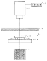
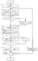
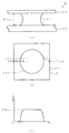
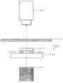
| JP3902017B2 (ja) | 半田高さ計測装置およびその方法 | |
| JP4449596B2 (ja) | 実装基板検査装置 | |
| JP2000352559A (ja) | 接合検査装置及び方法 | |
| JP3978507B2 (ja) | バンプ検査方法及び装置 | |
| JP5569061B2 (ja) | X線検査方法、x線検査装置およびx線検査プログラム | |
| JP2003240736A (ja) | X線断層面検査方法、及びx線断層面検査装置 | |
| JP2007139676A (ja) | 基板の検査装置及び検査方法 | |
| JPH04359447A (ja) | 半導体装置のハンダ接合部検査装置 | |
| JP2006220424A (ja) | X線ct検査装置及びx線ct検査方法 |
Legal Events
| Date | Code | Title | Description |
|---|---|---|---|
| A521 | Written amendment |
Free format text: JAPANESE INTERMEDIATE CODE: A523 Effective date: 20041213 |
|
| A621 | Written request for application examination |
Free format text: JAPANESE INTERMEDIATE CODE: A621 Effective date: 20041213 |
|
| A977 | Report on retrieval |
Free format text: JAPANESE INTERMEDIATE CODE: A971007 Effective date: 20061221 |
|
| TRDD | Decision of grant or rejection written | ||
| A01 | Written decision to grant a patent or to grant a registration (utility model) |
Free format text: JAPANESE INTERMEDIATE CODE: A01 Effective date: 20061227 |
|
| A61 | First payment of annual fees (during grant procedure) |
Free format text: JAPANESE INTERMEDIATE CODE: A61 Effective date: 20061227 |
|
| R150 | Certificate of patent or registration of utility model |
Free format text: JAPANESE INTERMEDIATE CODE: R150 |
|
| FPAY | Renewal fee payment (event date is renewal date of database) |
Free format text: PAYMENT UNTIL: 20110112 Year of fee payment: 4 |
|
| FPAY | Renewal fee payment (event date is renewal date of database) |
Free format text: PAYMENT UNTIL: 20110112 Year of fee payment: 4 |
|
| FPAY | Renewal fee payment (event date is renewal date of database) |
Free format text: PAYMENT UNTIL: 20120112 Year of fee payment: 5 |
|
| LAPS | Cancellation because of no payment of annual fees |