JP3794792B2 - Circuit board - Google Patents
Circuit board Download PDFInfo
- Publication number
- JP3794792B2 JP3794792B2 JP21021597A JP21021597A JP3794792B2 JP 3794792 B2 JP3794792 B2 JP 3794792B2 JP 21021597 A JP21021597 A JP 21021597A JP 21021597 A JP21021597 A JP 21021597A JP 3794792 B2 JP3794792 B2 JP 3794792B2
- Authority
- JP
- Japan
- Prior art keywords
- bonding
- pattern portion
- circuit board
- conductor
- conductor pattern
- Prior art date
- Legal status (The legal status is an assumption and is not a legal conclusion. Google has not performed a legal analysis and makes no representation as to the accuracy of the status listed.)
- Expired - Fee Related
Links
Images
Classifications
-
- H—ELECTRICITY
- H05—ELECTRIC TECHNIQUES NOT OTHERWISE PROVIDED FOR
- H05K—PRINTED CIRCUITS; CASINGS OR CONSTRUCTIONAL DETAILS OF ELECTRIC APPARATUS; MANUFACTURE OF ASSEMBLAGES OF ELECTRICAL COMPONENTS
- H05K3/00—Apparatus or processes for manufacturing printed circuits
- H05K3/30—Assembling printed circuits with electric components, e.g. with resistors
- H05K3/32—Assembling printed circuits with electric components, e.g. with resistors electrically connecting electric components or wires to printed circuits
- H05K3/328—Assembling printed circuits with electric components, e.g. with resistors electrically connecting electric components or wires to printed circuits by welding
-
- H—ELECTRICITY
- H05—ELECTRIC TECHNIQUES NOT OTHERWISE PROVIDED FOR
- H05K—PRINTED CIRCUITS; CASINGS OR CONSTRUCTIONAL DETAILS OF ELECTRIC APPARATUS; MANUFACTURE OF ASSEMBLAGES OF ELECTRICAL COMPONENTS
- H05K1/00—Printed circuits
- H05K1/02—Details
- H05K1/11—Printed elements for providing electric connections to or between printed circuits
- H05K1/111—Pads for surface mounting, e.g. lay-out
-
- H—ELECTRICITY
- H05—ELECTRIC TECHNIQUES NOT OTHERWISE PROVIDED FOR
- H05K—PRINTED CIRCUITS; CASINGS OR CONSTRUCTIONAL DETAILS OF ELECTRIC APPARATUS; MANUFACTURE OF ASSEMBLAGES OF ELECTRICAL COMPONENTS
- H05K1/00—Printed circuits
- H05K1/02—Details
- H05K1/0213—Electrical arrangements not otherwise provided for
- H05K1/0237—High frequency adaptations
- H05K1/0243—Printed circuits associated with mounted high frequency components
-
- H—ELECTRICITY
- H05—ELECTRIC TECHNIQUES NOT OTHERWISE PROVIDED FOR
- H05K—PRINTED CIRCUITS; CASINGS OR CONSTRUCTIONAL DETAILS OF ELECTRIC APPARATUS; MANUFACTURE OF ASSEMBLAGES OF ELECTRICAL COMPONENTS
- H05K2201/00—Indexing scheme relating to printed circuits covered by H05K1/00
- H05K2201/09—Shape and layout
- H05K2201/09209—Shape and layout details of conductors
- H05K2201/09654—Shape and layout details of conductors covering at least two types of conductors provided for in H05K2201/09218 - H05K2201/095
- H05K2201/0969—Apertured conductors
-
- H—ELECTRICITY
- H05—ELECTRIC TECHNIQUES NOT OTHERWISE PROVIDED FOR
- H05K—PRINTED CIRCUITS; CASINGS OR CONSTRUCTIONAL DETAILS OF ELECTRIC APPARATUS; MANUFACTURE OF ASSEMBLAGES OF ELECTRICAL COMPONENTS
- H05K2201/00—Indexing scheme relating to printed circuits covered by H05K1/00
- H05K2201/10—Details of components or other objects attached to or integrated in a printed circuit board
- H05K2201/10007—Types of components
- H05K2201/10083—Electromechanical or electro-acoustic component, e.g. microphone
-
- H—ELECTRICITY
- H05—ELECTRIC TECHNIQUES NOT OTHERWISE PROVIDED FOR
- H05K—PRINTED CIRCUITS; CASINGS OR CONSTRUCTIONAL DETAILS OF ELECTRIC APPARATUS; MANUFACTURE OF ASSEMBLAGES OF ELECTRICAL COMPONENTS
- H05K2203/00—Indexing scheme relating to apparatus or processes for manufacturing printed circuits covered by H05K3/00
- H05K2203/02—Details related to mechanical or acoustic processing, e.g. drilling, punching, cutting, using ultrasound
- H05K2203/0285—Using ultrasound, e.g. for cleaning, soldering or wet treatment
-
- H—ELECTRICITY
- H05—ELECTRIC TECHNIQUES NOT OTHERWISE PROVIDED FOR
- H05K—PRINTED CIRCUITS; CASINGS OR CONSTRUCTIONAL DETAILS OF ELECTRIC APPARATUS; MANUFACTURE OF ASSEMBLAGES OF ELECTRICAL COMPONENTS
- H05K2203/00—Indexing scheme relating to apparatus or processes for manufacturing printed circuits covered by H05K3/00
- H05K2203/04—Soldering or other types of metallurgic bonding
- H05K2203/049—Wire bonding
-
- H—ELECTRICITY
- H10—SEMICONDUCTOR DEVICES; ELECTRIC SOLID-STATE DEVICES NOT OTHERWISE PROVIDED FOR
- H10W—GENERIC PACKAGES, INTERCONNECTIONS, CONNECTORS OR OTHER CONSTRUCTIONAL DETAILS OF DEVICES COVERED BY CLASS H10
- H10W72/00—Interconnections or connectors in packages
- H10W72/071—Connecting or disconnecting
- H10W72/072—Connecting or disconnecting of bump connectors
- H10W72/07231—Techniques
- H10W72/07232—Compression bonding, e.g. thermocompression bonding
- H10W72/07233—Ultrasonic bonding, e.g. thermosonic bonding
-
- H—ELECTRICITY
- H10—SEMICONDUCTOR DEVICES; ELECTRIC SOLID-STATE DEVICES NOT OTHERWISE PROVIDED FOR
- H10W—GENERIC PACKAGES, INTERCONNECTIONS, CONNECTORS OR OTHER CONSTRUCTIONAL DETAILS OF DEVICES COVERED BY CLASS H10
- H10W72/00—Interconnections or connectors in packages
- H10W72/071—Connecting or disconnecting
- H10W72/072—Connecting or disconnecting of bump connectors
- H10W72/07231—Techniques
- H10W72/07236—Soldering or alloying
-
- Y—GENERAL TAGGING OF NEW TECHNOLOGICAL DEVELOPMENTS; GENERAL TAGGING OF CROSS-SECTIONAL TECHNOLOGIES SPANNING OVER SEVERAL SECTIONS OF THE IPC; TECHNICAL SUBJECTS COVERED BY FORMER USPC CROSS-REFERENCE ART COLLECTIONS [XRACs] AND DIGESTS
- Y02—TECHNOLOGIES OR APPLICATIONS FOR MITIGATION OR ADAPTATION AGAINST CLIMATE CHANGE
- Y02P—CLIMATE CHANGE MITIGATION TECHNOLOGIES IN THE PRODUCTION OR PROCESSING OF GOODS
- Y02P70/00—Climate change mitigation technologies in the production process for final industrial or consumer products
- Y02P70/50—Manufacturing or production processes characterised by the final manufactured product
Landscapes
- Engineering & Computer Science (AREA)
- Microelectronics & Electronic Packaging (AREA)
- Manufacturing & Machinery (AREA)
- Electric Connection Of Electric Components To Printed Circuits (AREA)
- Manufacturing Of Printed Wiring (AREA)
- Combinations Of Printed Boards (AREA)
Description
【0001】
【発明の属する技術分野】
本発明は、基板上の導体層をパターン形成して導体パターン部とした回路基板に係り、特に、導体パターン部にボンディングエリアを定め、超音波ボンディング方法を用いて基板上に実装する部品のバンプを接合する回路基板に関するものである。
【0002】
【従来の技術】
基板上に銅箔等の導体層を接着して積層し、導体層を所望のパターン形状に形成して配線接続を実現する回路基板は、大型な電子装置に用いられるカード型のプリント基板としてだけでなく、最近では、マルチチップ実装やベアチップ実装等の高密度実装方法が普及したことにより、大小さまざまな回路基板が多様に使われている。例えば、チップ部品を回路基板に直接にフェースダウンボンディングする回路基板や、バンプやタブを直接に回路基板上に超音波ボンディングすることができる回路基板、あるいは、配線基板であると同時に部品の容器をも兼ねて電子部品に使われる回路基板等にもその例を見ることができる。
【0003】
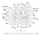
以下、従来技術を総合的に駆使して高密度実装化に対応する最近の回路基板の1例として、チップ型表面弾性波素子に用いられる回路基板を例に取り、図11乃至図12を参照して説明する。
【0004】
図11は従来の表面弾性波素子の構造を分解図として示す斜視図である。ニオブ酸リチウム結晶等の表面弾性波チップ(以下、チップという)21の片面(図11においては裏面)には、信号入出力用、グランド接続用、あるいは、必要により電源接続用等の目的で、高さが数十ミクロン程度の複数の電極バンプ(以下、バンプという)22が8カ所に取り付けられている。チップ21が搭載される回路基板23には、導体パターン部24が導体層にパターン形成されており、導体パターン部24には、バンプ22が超音波ボンディングされて固着される所定の領域として、ボンディングエリア25が定められている。ここで、ボンディングエリア25は、バンプ22が直接当たるボンディング位置と超音波ボンディングにより当該バンプが広がって溶着、接合した部分とを包含するエリアである。そして、前記チップ21が超音波ボンディングで装着されたのち、回路基板23は容器26に収納されて蓋27により封止される。このような従来技術の例は、特開平4−65909号公報にも見ることができる。
【0005】
回路基板23は、一般に厚さ0.2〜2.5ミリ程度の樹脂やセラミックス等の絶縁基材上に厚さ数十ミクロン程度の接着層を介して厚さ12〜75ミクロン程度の銅等の金属箔が導体層として積層され、導体層が所望のパターン形状にエッチングされ、導体パターン部24による平面状の回路を構成している。なお、最近の回路基板では、導体層が数百ミクロン程度の幅やスペースでエッチングされ、高精度な導体パターン部を形成している。
【0006】
上記の回路基板にバンプ付きの部品を実装する超音波ボンディングについて、図12を参照して以下に説明する。まず、超音波ボンダー28のヘッド部29の先端でバンプ22を下面にしてチップ21を吸着し、次いで、複数のバンプ22のそれぞれを回路基板23上の導体パターン部24のボンディングエリア中心(ボンディング位置)に位置合わせし、ヘッド部29を下ろしてバンプ22を導体パターン部24の表面に押し付けるとともに、ヘッド部29からチップ21経由で超音波をバンプ22に加え、超音波のエネルギーを利用してバンプ22と導体パターン部24を接合させ、回路基板23にチップ21を固着させる。
【0007】
【発明が解決しようとする課題】
しかしながら、上記の従来の技術によると、次のような種々の未解決な課題が残されていた。
【0008】
すなわち、複数のバンプを備えた部品を回路基板上に超音波ボンディングする場合、全てのバンプに同程度のボンディング強度を持たせることが難しく、バンプ毎のボンディング強度にバラツキが生じてしまう。
【0009】
バンプをボンディングエリアに超音波ボンディングする場合には、本来はバンプの形状やボンディングエリアを含めた導体パターン部の形状等に応じて、最適な超音波の接合エネルギーをバンプに加えることが望ましい。例えば、図11の導体パターン部24のうち導体ランド24aに示すように三方向がパターンの境界で仕切られた比較的に幅の狭い導体ランド部分のボンディングエリアに対してバンプを超音波ボンディングする場合には、バンプには比較的強い超音波エネルギーを時間も長く加え、チップに加える荷重も大きくしてボンディングエリアにボンディングすることが望ましい。
【0010】
また、図11の導体パターン部24のうち導体ランド24bに示すような比較的に幅の広い導体ランド部分のボンディングエリアにバンプを超音波ボンディングする場合には、上記のような強い超音波エネルギーや荷重をバンプに加える必要はなく、反対に、あまり強い超音波エネルギーをバンプに加えると、かえって回路基板やチップにクラックを生じる等、破損してしまう等の問題が起きる。
【0011】
しかしながら、一方では、回路基板に形成した導体パターン部の形状や面積は、電気信号の種類や電流容量、あるいは、パターンの用途等によって多様に異なるのが通常であるのにも拘わらず、他方では、超音波ボンダーのヘッド部からチップに加わる超音波エネルギーは、チップが導体パターン部に押し当てられることによって各バンプに機械的に単純に配分されるに過ぎない。
【0012】
その結果、それぞれのボンディングエリアに対して組合わされる個々のバンプには、それぞれに適した超音波エネルギーを各別に加えることが望ましいものの、実際には接合エネルギーの調整が不可能であり、結果として、複数のバンプが付いたチップを回路基板に超音波ボンディングする場合には、バンプとボンディングエリアの接合に働く接合エネルギーに過不足が生じ、超音波ボンディングの不良率が高く、接合部の信頼性にも欠けるものであった。
【0013】
さらに、最近の傾向であるフレキシブルマニュファクチャリングシステムやロボット化した自動実装装置を例にとれば、一台の超音波ボンダーを用いて、多種類の回路基板に対して、バンプ付きのチップを超音波ボンディングする場合や、大型回路基板の各所に多種類のバンプ付き部品を超音波ボンディングするマルチチップ実装等の場合には、回路基板の種類が変わる毎に、あるいは、導体パターン部の形状が異なる毎に、さらには、部品のバンプ数が異なる毎に、その都度、最適なボンディング条件になるように超音波ボンダーの動作条件を調整し直さなければならず、実質的に生産性が極端に低下するので実用性に欠けるという重大な欠点があった。
【0014】
結果的に、バンプ付きのチップを回路基板に実装する場合には、超音波ボンディングは汎用性に欠け、生産性に乏しく、しかも、接合後の信頼性にも欠けるという課題を有していた。
【0015】
本発明は、上記の課題に鑑みてなされたものであり、回路基板の導体パターン部のボンディングエリアにバンプ付きのチップをバラツキが少なく、高いボンディング強度で固着することができる回路基板を提供することを目的とする。
【0016】
本発明のその他の目的や新規な特徴は後述の実施の形態において明らかにする。
【0017】
【課題を解決するための手段】
上記目的を達成するために、本発明に係る第1の回路基板は、基板本体上に設けられた導体層にパターンが形成された導体パターン部を有し、超音波ボンディングで搭載される部品のバンプが当たるボンディング位置を含むボンディングエリアが前記導体パターン部に2つ以上設定される場合において、
前記ボンディングエリアが2つ以上設定された前記導体パターン部における、前記部品に備わる複数のバンプが超音波ボンディングされる少なくとも1つのボンディング位置の近傍の導体層に、前記ボンディングエリアに加わる接合エネルギーを揃えるように孤立した切欠部又は凹部が形成されていることを特徴としている。
【0018】
また、本発明に係る第2の回路基板は、基板本体上に設けられた導体層にパターンが形成された導体パターン部を有し、超音波ボンディングで搭載される部品のバンプが当たるボンディング位置を含むボンディングエリアが前記導体パターン部に2つ以上設定される場合において、
前記ボンディングエリアが2つ以上設定された前記導体パターン部における、前記部品に備わる複数のバンプが超音波ボンディングされる少なくとも1つのボンディング位置の近傍の導体層に、前記ボンディングエリアに加わる接合エネルギーを揃えるように前記導体パターン部の縁から内側に延びてボンディング位置近傍に至る切欠部又は凹部が形成されていることを特徴としている。
【0019】
前記第1又は第2の回路基板において、前記切欠部又は凹部が前記超音波ボンディングの超音波振動の方向を横切る方向に延びて形成されているとよい。
【0020】
本発明に係る第3の回路基板は、基板本体上に設けられた導体層にパターンが形成された導体パターン部を有し、超音波ボンディングで搭載される部品のバンプが当たるボンディング位置が前記導体パターン部に2つ以上設定される場合において、
前記ボンディング位置が2つ以上設定された前記導体パターン部における、前記部品に備わる複数のバンプが超音波ボンディングされる少なくとも1つのボンディング位置の近傍の導体層に、孤立した切欠部又は凹部が形成されており、前記切欠部又は凹部が前記超音波ボンディングの超音波振動の方向を横切る方向に延びて形成されていることを特徴としている。
本発明に係る第4の回路基板は、基板本体上に設けられた導体層にパターンが形成された導体パターン部を有し、超音波ボンディングで搭載される部品のバンプが当たるボンディング位置が前記導体パターン部に2つ以上設定される場合において、
前記ボンディング位置が2つ以上設定された前記導体パターン部における、前記部品に備わる複数のバンプが超音波ボンディングされる少なくとも1つのボンディング位置の近傍の導体層に、前記導体パターン部の縁から内側に延びてボンディング位置近傍に至る切欠部又は凹部が形成されており、前記切欠部又は凹部が前記超音波ボンディングの超音波振動の方向を横切る方向に延びて形成されていることを特徴としている。
また、前記回路基板において、前記切欠部又は凹部が前記導体パターン部を部分的に狭隘にして狭隘パターン部を形成するものであってもよい。
【0021】
【発明の実施の形態】
以下、本発明に係る回路基板の実施の形態を図面に従って説明する。
【0022】
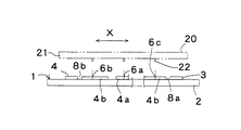
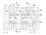
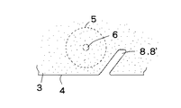
図1は本発明に係る回路基板の第1の実施の形態を示す平面図、図2は正断面図である。これらの図に示すように、回路基板1は、基板本体2上に導体層3を積層し、導体層3に所望の形状のパターンを形成した導体パターン部4を構成したものである。回路基板1上にフェースダウン実装される図2の仮想線で示す部品20は、1つのチップ21に複数のバンプ22が設けられており(例えば図11に示したチップと同様のもの)、導体パターン部4には、バンプが超音波ボンディング方法により固着される領域として複数のボンディングエリア5a,5b,5cが定められている。ここで、ボンディングエリアは、バンプ22が直接当たるボンディング位置と超音波ボンディングにより当該バンプが広がって溶着した部分とを包含するエリアである。
【0023】
ボンディングエリア5aは、導体パターン部4のうち、信号授受のための比較的導体パターン幅が狭い導体ランド4aにあり、ボンディングエリア5b,5cはグランドや電源となる比較的導体パターン幅が広い導体ランド4bにある。ボンディングエリア5a,5b,5cの中央部は、バンプが導体層3に押し付けられるボンディング位置6a,6b,6cである。さらに、導体パターン部4の導体ランド4a,4bが延びて回路基板1の縁には、回路基板と外部を接続する端子部7が設けられている。
【0024】
前記基板本体2を形成する材料は十分な強度を有する材料であればよく、絶縁性のエポシキ樹脂やセラミックス、あるいは、金属板上に絶縁層を積層したメタル基板等でもよい。また、導体層は、電気信号を伝送できる導電性材料であればよく、銅や金、ニッケル等の金属箔や焼成厚膜導体層等の導体であればよい。また、これらの導体の表面にニッケルや金等メッキ層が施されることによりボンディング性を良くすることもできる。
【0025】
本発明の第1の実施の形態の要部として、導体パターン部4に含まれるボンディングエリア5a,5b,5cの縁にあたる導体層部分(ボンディングエリア5a,5b,5cの内又は近傍、つまりボンディング位置6a,6b,6cの近傍)には、超音波ボンディングを良好に行えるように、切欠部8a,8bが設けられている。これらの切欠部8a,8bは電気接続のためには必要とされないものである。また、それらの切欠部8aと切欠部8bは、共に設けられる必要はない。ここで、切欠部8aは、ボンディングエリア5cのある導体層3の周囲の三方を囲み、一端がボンディングエリア5cの縁又は近傍に達した所で止まり、他端が導体パターン部4の縁に達するまで長く延びた導体層が欠落した空白パターンである。図1の平面図によれば、切欠部8aは、導体パターン部4の縁から導体パターン部4の内側に延びてボンディングエリア5cの縁に達する帯状のスリットとして形成されている。また、切欠部8bは、導体パターン部4の縁から隔たった導体パターン部4の内側に孤立する空白パターンであり、導体パターン部の縁に対して不連続な島状のスリットとして形成されている。なお、切欠部8a,8bは、導体層3が基板本体2に当初から被着されていない空白パターン、あるいは、基板本体2上に被着された導体層3が所定の幅で除去された空白パターンとして形成される。
【0026】
なお、図1中、超音波ボンディングの際に印加される超音波振動は矢印X方向であり、前記切欠部8a,8bは超音波振動の方向(X方向)を横切る向きの空白パターン部分を少なくとも有している。
【0027】
また、切欠部8a,8bは、実質的に各ボンディングエリアに加わる接合エネルギーが揃うように、回路基板1上のボンディングエリアに対する相対的な位置や形状を設定する。
【0028】
そして、この第1の実施の形態によれば、導体パターン部4のうち導体ランド4bに、超音波振動の方向(X方向)を横切る向きの切欠部8a,8bが設けられことにより、導体ランド4bのボンディングエリア5b,5cは、ボンディングエリア5b,5cに広がる導体層のX方向の領域が物理的に限定され、ボンディングエリア5b,5cにつながる導体ランド4bの導体層の幅は切欠部8a,8bによって狭く絞られた狭隘パターン部となるので、ボンディングエリア5aのある幅の狭い導体ランド4aの領域と近似する。つまり、超音波ボンディングの条件が相互に近似することになる。その結果、ボンディングエリア5a,5b,5cを含めた導体パターン部4に広狭があっても、どのボンディングエリアにも一様な超音波エネルギーが加わることになり、超音波ボンディングの際のチップ21側のバンプ22とボンディングエリアの導体層とに加わる接合エネルギーを揃えることができる。従って、バンプとボンディングエリアの接合に働く接合エネルギーに過不足が発生することを防止でき、接合不良の発生を防ぐことができる。なお、切欠部8a,8bが超音波振動の方向(X方向)を横切る向きの空白パターン部分を有するようにしたのは、ボンディングエリア5a,5b,5cの周囲の超音波振動方向(X方向)の導体層幅が超音波ボンディングの接合条件に大いに影響するからである。
【0029】
なお、この第1の実施の形態では、基板本体2として厚さ0.5ミリ、一辺が75ミリ四方のビスマレイミドトリアジン樹脂の積層基板を用い、導体層3としては、基板に積層した厚さ18ミクロンの銅箔上に厚さが10ミクロンの銅メッキ層と、厚さが5〜10ミクロンのニッケルメッキ層、厚さが0.5〜1ミクロンの金メッキ層を被覆して用いている。なお、回路基板1は、チップ実装後に数ミリ角にダイシングによってカットされ、最終的には図示の形状に分離される。回路基板上にフェースダウン実装する部品としては、ニオブ酸リチウム単結晶の表面弾性波チップ素子(図11で説明したチップ21と同様のもの)を用い、その片面には、径が25ミクロンの金バンプが8個所に設けられている。そして、ボンディングエリア5a,5b,5cの周りには、導体層をエッチングすることにより幅が50〜150ミクロンの細長いスリット状の空白パターンとなる切欠部を形成した。
【0030】
本実施の形態において、図2の仮想線に示したチップ21を図12に図示した如き超音波ボンダーのヘッド部に吸引させ、回路基板1のボンディングエリア5a,5b,5cに各バンプ22を位置合わせして100℃に加熱した条件下で押圧700gでバンプを導体層に押し付けながら、周波数60kHz、超音波出力1.5Wの超音波を0.5秒間、加えて超音波ボンディングを行った。
【0031】
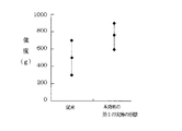
図4は、本実施の形態によって得られた超音波ボンディングの接合強度とバラツキを、せん断方向に応力を加えて測定し、従来技術による接合強度と比較したグラフを示している。超音波ボンディングを良好にするための切欠部を導体パターン部に有しない従来の回路基板では、平均の接合強度が500gであり、最大強度が700g、最低強度が300gであったのに比較し、この実施の形態によれば、平均の接合強度が760gに顕著に強化され、最大強度も900g、最低強度でも600gであった。
【0032】
さらに、注目すべきことに、破壊試験の結果によると、従来例によれば、バンプと基板上の金メッキの間で剥離する破壊モードが15%も生じているのに対して、本実施の形態の場合には、このような剥離モードが皆無であり、全てが素子の破壊か、あるいは、素子の電極自体の破壊等による破壊モードを示している。
【0033】
この第1の実施の形態によれば、搭載部品側のバンプとボンディングエリア5a、5b、5cに加わる超音波エネルギーは、導体パターン部4に切欠部8a,8bが設けられていることにより、各ボンディングエリア周囲の条件が揃えられ、過不足無く、有効に接合エネルギーとなって各バンプに作用し、強固でバラツキの少ないバンプのボンディングを実現することができるという著しい効果がある。この傾向は、特に樹脂基板を基板本体2に用いた場合には顕著である。
【0034】
なお、上記の第1の実施の形態の説明では、切欠部8a,8bについて、導体層3をスリット状にエッチングする例を挙げたが、厚膜導体層を形成する場合には、スクリーンでマスキングを行い、厚膜導体が基板本体上に被着しないようにすることによって切欠部を形成することもできる。もちろん、切欠部8a,8bをレーザ加工等により形成し、導体層3に後加工でスリットを切り込むこともできる。これによれば、試験的に回路基板上に部品を実際に取り付け、超音波ボンディングの接合強度のバラツキを計測し、その結果によって量産時の回路基板の切欠部を後加工する際の位置や長さ、形状を設定することができるという効果がある。
【0035】
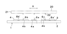
上記第1の実施の形態では、導体パターン部4に、基板本体2に至るまでの導体層3を厚み方向の全てにわたり除去した切欠部8a,8bを設けた場合を例示したが、必ずしも基板本体2に至るまでの導体層3の厚み方向全部を除去する必要はなく、超音波ボンディングの伝搬条件を実質的に揃えることができる程度に導体層の肉厚を薄くするように凹部を形成してもよく、この場合を本発明の第2の実施の形態として図3に示す。
【0036】
図3の第2の実施の形態では、第1の実施の形態の切欠部8a,8bの代わりに導体層3の肉厚を薄くして導体層3の厚みを一部残した凹部8a’,8b’を基板本体2上の導体パターン部4に形成している。その他の構成部分は前述の第1の実施の形態と同様であり、同一又は相当部分に同一符号を付して説明を省略する。
【0037】
この第2の実施の形態の場合も、各ボンディングエリア5a、5b、5c周囲の導体パターン部4の超音波ボンディングの条件を揃えることで、搭載部品側のバンプ22及びボンディングエリア5a、5b、5cに過不足無く超音波エネルギーを与えて、強固なバンプのボンディングを実現することができる。この第2の実施の形態は、レーザ加工等の後加工で凹部8a’,8b’を形成するのに好都合である。
【0038】
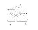
以上の本発明の第1及び第2の実施の形態では、1個の部品を回路基板上にフェースダウンボンディングすることを前提として説明したが、マルチチップ実装の場合にも、本質的に本発明は適用できるものであり、この場合を本発明の第3の実施の形態として図5で説明する。すなわち、図5に示すように、回路基板10上には、導体層3にパターンが形成された導体パターン部4が設けられており、回路基板10上には、バンプ数が異なる部品A、B、Cを搭載するために、それぞれの部品に備わる複数のバンプが超音波ボンディングされる領域として導体パターン部4にボンディングエリア5a,5bが設定されている。しかも、少なくとも1つのボンディングエリアの内または近傍(換言すれば、少なくとも1つのボンディング位置6a,6bの近傍)の導体層には空白パターンである切欠部8a,8bが設けられている。そして、部品A、B、Cに対応して、ボンディングエリアの内又は近傍の導体層に設けられる切欠部8a,8bは、それぞれの部品に対応して形状と配置が異なっている。特に、各部品A、B、Cが有するバンプの数(6個、8個、2個)に応じて切欠部8a,8bの位置や形状が異なって形成される点が先の第1の実施の形態とは異なる。その他の構成部分は前述の第1の実施の形態と同様であり、同一又は相当部分に同一符号を付して説明を省略する。
【0039】
この第3の実施の形態によれば、超音波ボンダーのヘッド部から部品に加わる超音波エネルギーや荷重が同じであっても、バンプの数に対応させて導体パターン部4に形成される切欠部8a,8bの形状あるいは位置がそれぞれの部品に適合するように設定されているので、バンプの数が異なる異種の部品を同一の回路基板に実装する場合にも、それぞれのバンプとボンディングエリアに加わる超音波の接合エネルギーを揃えることができる。とりわけ、超音波出力をプログラム設定することができない簡易な超音波ボンダーを用いることによっても、マルチチップ実装を実現できるという特別な効果がある。
【0040】
なお、第3の実施の形態において、切欠部8a,8bの代わりに導体層3の厚みの一部を残した凹部を形成するようにしても同様の効果が得られる。
【0041】
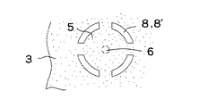
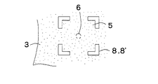
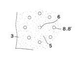
図6乃至図10は、超音波ボンディングを良好に行うために、ボンディングエリア5の内又は近傍、換言すればボンディング位置6の近傍に形成した切欠部8又は凹部8’の変形例をそれぞれ示す。ここで、切欠部8は導体層3の厚み方向全てを除去した空白パターン、凹部8’は導体層3の厚みの一部を残したものである。切欠部又は凹部は直線状又は矩形状のスリットに限らず、図6の円弧状切欠部8又は凹部8’、図7のL字状(鉤状)切欠部8又は凹部8’、図8の円形状(点状)切欠部8又は凹部8’であってもよく、ボンディング位置6を囲むように複数個設けるとよい。また、図9のように導体パターン部4の縁から斜めに傾斜させて導体層3に切欠部8又は凹部8’を形成してもよく、図10のように導体パターン部4の縁から二股に分岐させて導体層3に切欠部8又は凹部8’を形成してもよい。
【0042】
さらに、図示はしないが、切欠部又は凹部をくさび形、ジグザグ形状等、状況に応じて最適な形状に設定することも本発明に含まれる。特に、十文字型のスリット形状とすれば、ボンディング時の位置決めの目標になり、コーナーマークやオリエンテーションマーク、極性マーク等としても利用できるという効果がある。
【0043】
いずれにしても、導体パターン部のボンディングエリアにバンプから加わる超音波エネルギーは、幅広な導体ランドに切欠部や凹部がない場合に比べて、ボンディング位置の近傍の導体層に切欠部又は凹部が設けられることによって、幅の狭い導体ランドと同様の伝搬条件で加わることになる。その結果、幅狭な導体パターン部のボンディングエリアにバンプを超音波ボンディングする場合と同等のボンディング条件で過不足の無い超音波エネルギーでボンディングできるという効果がある。
【0044】
上記の切欠部又は凹部の形成は、導体パターン部の複数の導体ランドのうち、幅が比較的に狭い入出力信号用の導体ランドよりも、幅が比較的に広い導体ランドとなる部分、例えばグランドパターンやシールドパターン、あるいは、電源パターンや補強用の捨てパターン等に適用すると、格別の効果がある。
【0045】
なお、本発明による切欠部又は凹部は、回路基板上の全ての導体ランドに設ける必要がないことはもちろんである。
【0046】
以上、本発明の実施形態について説明して来たが、本発明は、これに限定されることなく、本発明の技術的思想の範囲内において、各種の改変が可能なことは自明である。
【0047】
【発明の効果】
以上説明したように、本発明によれば、基板本体上に設けられた導体層にパターンが形成された導体パターン部を有し、超音波ボンディングで搭載される部品のバンプが当たるボンディング位置が前記導体パターン部に2つ以上設定される回路基板において、前記ボンディング位置が2つ以上設定された前記導体パターン部における、少なくとも1つのボンディング位置の近傍の導体層に、孤立した切欠部又は凹部、あるいは前記導体パターン部の縁から内側に延びてボンディング位置近傍に至る切欠部又は凹部が形成されているので、それぞれのボンディング位置を含むボンディングエリアにおいて実質的にボンディングエリアに加わる接合エネルギーを揃えることが可能となる。この結果、複数のバンプが付いたチップを回路基板に超音波ボンディングする場合にも、バンプとボンディングエリアの接合に働く接合エネルギーに過不足が生じることなく、超音波ボンディングの接合強度を高めてバラツキを減少させ、超音波ボンディングの不良率を著しく低下させ、信頼性の優れた超音波ボンディングを実現できる回路基板を提供できるという優れた効果を奏する。
【図面の簡単な説明】
【図1】本発明に係る回路基板の第1の実施の形態を示す平面図である。
【図2】同断面図である。
【図3】本発明の第2の実施の形態を示す断面図である。
【図4】本発明の第1の実施の形態の場合の回路基板の強度試験結果を従来の場合と比較して示す説明図である。
【図5】本発明の第3の実施の形態を示す平面図である。
【図6】本発明に係る切欠部又は凹部の変形例であって円弧状の場合の平面図である。
【図7】本発明に係る切欠部又は凹部の変形例であってL字状の場合の平面図である。
【図8】本発明に係る切欠部又は凹部の変形例であって円形状の場合の平面図である。
【図9】本発明に係る切欠部又は凹部の変形例であって導体パターン部の縁から斜めに形成されたスリットの場合の平面図である。
【図10】本発明に係る切欠部又は凹部の変形例であって導体パターン部の縁から2股状に形成されたスリットの場合の平面図である。
【図11】従来技術を説明する分解斜視図である。
【図12】超音波ボンディングを説明する説明図である。
【符号の説明】
1,10,23 回路基板
2 基板本体
3 導体層
4,24 導体パターン部
4a,4b 導体ランド
5,5a,5b,5c ボンディングエリア
6,6a,6b,6c ボンディング位置
7 端子部
8,8a,8b 切欠部
8’,8a’,8b’ 凹部[0001]
BACKGROUND OF THE INVENTION
The present invention relates to a circuit board in which a conductor layer on a substrate is patterned to form a conductor pattern portion, and in particular, a bonding area is defined in the conductor pattern portion, and a bump of a component mounted on the substrate using an ultrasonic bonding method It is related with the circuit board which joins.
[0002]
[Prior art]
A circuit board that realizes wiring connection by bonding a conductor layer such as copper foil on a board and laminating it and forming the conductor layer in a desired pattern shape is only as a card-type printed board used in large electronic devices Recently, high-density mounting methods such as multichip mounting and bare chip mounting have become widespread, and various circuit boards of various sizes have been used. For example, a circuit board in which chip components are directly face-down bonded to a circuit board, a circuit board in which bumps and tabs can be directly ultrasonically bonded to the circuit board, or a wiring board and a container for components at the same time An example can also be seen on circuit boards used for electronic components.
[0003]
Hereinafter, a circuit board used for a chip-type surface acoustic wave device will be taken as an example of a recent circuit board corresponding to high-density mounting by making full use of conventional technology, and see FIGS. 11 to 12. To explain.
[0004]
FIG. 11 is a perspective view showing the structure of a conventional surface acoustic wave device as an exploded view. On one surface (the back surface in FIG. 11) of a surface acoustic wave chip (hereinafter referred to as a chip) 21 such as a lithium niobate crystal, for the purpose of signal input / output, ground connection, or power connection if necessary, etc. A plurality of electrode bumps (hereinafter referred to as bumps) 22 having a height of about several tens of microns are attached at eight locations. On the
[0005]
The
[0006]
Ultrasonic bonding for mounting a component with a bump on the circuit board will be described below with reference to FIG. First, the tip of the
[0007]
[Problems to be solved by the invention]
However, according to the above-described conventional technology, the following various unsolved problems remain.
[0008]
That is, when a component having a plurality of bumps is ultrasonically bonded onto a circuit board, it is difficult to give all the bumps the same bonding strength, and the bonding strength varies from bump to bump.
[0009]
When the bump is ultrasonically bonded to the bonding area, it is originally desirable to apply optimum ultrasonic bonding energy to the bump in accordance with the shape of the bump, the shape of the conductor pattern portion including the bonding area, and the like. For example, when bumps are ultrasonically bonded to a bonding area of a relatively narrow conductor land portion in which three directions are partitioned by a pattern boundary as shown in a
[0010]
In addition, when the bump is ultrasonically bonded to the bonding area of the relatively wide conductor land portion as shown in the
[0011]
However, on the other hand, the shape and area of the conductor pattern portion formed on the circuit board is usually variously different depending on the type of electric signal, the current capacity, or the use of the pattern. The ultrasonic energy applied to the chip from the head part of the ultrasonic bonder is merely mechanically distributed to each bump by pressing the chip against the conductor pattern part.
[0012]
As a result, although it is desirable to add ultrasonic energy suitable for each bump to each bonding area, it is actually impossible to adjust the bonding energy. When a chip with multiple bumps is ultrasonically bonded to a circuit board, excess and deficiency occurs in the bonding energy that works to bond the bump and bonding area, resulting in a high defect rate of ultrasonic bonding and the reliability of the bonded portion. It was also lacking.
[0013]
Furthermore, taking the recent trend of flexible manufacturing systems and robotized automatic mounting equipment as an example, a single ultrasonic bonder is used to superimpose bumped chips on many types of circuit boards. In the case of sonic bonding or multi-chip mounting in which various types of bumped parts are ultrasonically bonded to various parts of a large circuit board, the shape of the conductor pattern part changes each time the type of the circuit board changes. Every time, and every time the number of bumps on the parts is different, the operating conditions of the ultrasonic bonder must be adjusted again so that the optimum bonding conditions are obtained. Therefore, there was a serious drawback that it was not practical.
[0014]
As a result, when a chip with bumps is mounted on a circuit board, ultrasonic bonding has a problem of lack of versatility, poor productivity, and lack of reliability after bonding.
[0015]
The present invention has been made in view of the above problems, and provides a circuit board capable of fixing a chip with a bump to a bonding area of a conductor pattern portion of a circuit board with little variation and fixing with a high bonding strength. With the goal.
[0016]
Other objects and novel features of the present invention will be clarified in embodiments described later.
[0017]
[Means for Solving the Problems]
In order to achieve the above object, a first circuit board according to the present invention has a conductor pattern part in which a pattern is formed on a conductor layer provided on a board body, and is a component mounted by ultrasonic bonding. Bonding position where bump hitsBonding area includingWhen two or more are set in the conductor pattern portion,
BondingareaIn the conductor pattern portion in which two or more are set,A plurality of bumps on the component are ultrasonically bonded.On a conductor layer in the vicinity of at least one bonding position;To align the bonding energy applied to the bonding areaAn isolated notch or recess is formed.
[0018]
The second circuit board according to the present invention has a conductor pattern portion in which a pattern is formed on a conductor layer provided on the substrate body, and a bonding position where a bump of a component mounted by ultrasonic bonding hits.Bonding area includingWhen two or more are set in the conductor pattern portion,
BondingareaIn the conductor pattern portion in which two or more are set,A plurality of bumps on the component are ultrasonically bonded.On a conductor layer in the vicinity of at least one bonding position;To align the bonding energy applied to the bonding areaA notch or a recess extending inward from the edge of the conductor pattern portion and reaching the vicinity of the bonding position is formed.
[0019]
In the first or second circuit board, the notch or the recess may be formed to extend in a direction crossing a direction of ultrasonic vibration of the ultrasonic bonding.
[0020]
A third circuit board according to the present invention has a conductor pattern portion in which a pattern is formed on a conductor layer provided on a substrate body, and a bonding position where a bump of a component mounted by ultrasonic bonding hits the conductor. When two or more patterns are set,
An isolated notch or recess is formed in a conductor layer in the vicinity of at least one bonding position where a plurality of bumps provided in the component are ultrasonically bonded in the conductor pattern portion in which two or more bonding positions are set. The notch or recess is formed so as to extend in a direction crossing the direction of ultrasonic vibration of the ultrasonic bonding.
A fourth circuit board according to the present invention has a conductor pattern portion in which a pattern is formed on a conductor layer provided on a substrate body, and a bonding position where a bump of a component mounted by ultrasonic bonding hits the conductor. When two or more patterns are set,
In the conductor pattern portion in which two or more bonding positions are set, a plurality of bumps provided in the component are ultrasonically bonded to a conductor layer in the vicinity of at least one bonding position, from the edge of the conductor pattern portion to the inside. A notch or a recess extending to the vicinity of the bonding position is formed, and the notch or recess extends in a direction crossing the direction of ultrasonic vibration of the ultrasonic bonding.
Also,In the circuit board,The notch or the recess may partially narrow the conductor pattern portion to form a narrow pattern portion.
[0021]
DETAILED DESCRIPTION OF THE INVENTION
Embodiments of a circuit board according to the present invention will be described below with reference to the drawings.
[0022]
FIG. 1 is a plan view showing a first embodiment of a circuit board according to the present invention, and FIG. 2 is a front sectional view. As shown in these drawings, the
[0023]
The bonding area 5a is in the
[0024]
The material for forming the
[0025]
As a main part of the first embodiment of the present invention, a conductor layer portion (inside or near the
[0026]
In FIG. 1, the ultrasonic vibration applied at the time of ultrasonic bonding is in the direction of arrow X, and the
[0027]
Further, the
[0028]
According to the first embodiment, the
[0029]
In the first embodiment, a laminated substrate of bismaleimide triazine resin having a thickness of 0.5 mm and a side of 75 mm is used as the
[0030]
In the present embodiment, the
[0031]
FIG. 4 shows a graph in which the bonding strength and variation of the ultrasonic bonding obtained by this embodiment are measured by applying stress in the shear direction and compared with the bonding strength according to the prior art. In the conventional circuit board which does not have a notch for making ultrasonic bonding good in the conductor pattern part, the average bonding strength is 500 g, the maximum strength is 700 g, and the minimum strength is 300 g, According to this embodiment, the average bonding strength was remarkably strengthened to 760 g, the maximum strength was 900 g, and the minimum strength was 600 g.
[0032]
Furthermore, it should be noted that, according to the result of the destructive test, according to the conventional example, the destructive mode in which separation occurs between the bump and the gold plating on the substrate occurs as much as 15%. In the case of (2), there is no such peeling mode, and all indicate a destruction mode due to destruction of the element or destruction of the electrode of the element itself.
[0033]
According to the first embodiment, the ultrasonic energy applied to the bumps on the mounting component side and the
[0034]
In the description of the first embodiment, the example in which the
[0035]
In the first embodiment, the case where the
[0036]
In the second embodiment shown in FIG. 3, in place of the
[0037]
Also in the case of the second embodiment, the
[0038]
The first and second embodiments of the present invention have been described on the assumption that one component is face-down bonded on a circuit board. However, the present invention is essentially applicable to the case of multichip mounting. Is applicable, and this case will be described with reference to FIG. 5 as a third embodiment of the present invention. That is, as shown in FIG. 5, a
[0039]
According to the third embodiment, even if the ultrasonic energy and the load applied to the component from the head part of the ultrasonic bonder are the same, the notch part formed in the
[0040]
In the third embodiment, the same effect can be obtained by forming a recess leaving a part of the thickness of the
[0041]
FIGS. 6 to 10 show modifications of the
[0042]
Furthermore, although not shown, it is also included in the present invention to set the notch or recess to an optimum shape according to the situation, such as a wedge shape or a zigzag shape. In particular, if the cross-shaped slit shape is used, it becomes a positioning target during bonding and can be used as a corner mark, an orientation mark, a polarity mark, or the like.
[0043]
In any case, the ultrasonic energy applied from the bump to the bonding area of the conductor pattern part is provided with a notch or a recess in the conductor layer near the bonding position, compared to when the wide conductor land has no notch or recess. As a result, the same propagation condition as that of a narrow conductor land is applied. As a result, there is an effect that bonding can be performed with ultrasonic energy without excess or deficiency under the same bonding conditions as those in the case where the bump is ultrasonically bonded to the bonding area of the narrow conductor pattern portion.
[0044]
The formation of the above-mentioned notch or recess is a portion of the plurality of conductor lands in the conductor pattern portion that becomes a conductor land having a relatively wider width than the conductor land for an input / output signal having a relatively narrow width, for example, When applied to a ground pattern, a shield pattern, a power supply pattern, a reinforcing discard pattern, etc., there is a special effect.
[0045]
Of course, the notches or recesses according to the present invention need not be provided in all the conductor lands on the circuit board.
[0046]
The embodiment of the present invention has been described above, but the present invention is not limited to this, and it is obvious that various modifications can be made within the scope of the technical idea of the present invention.
[0047]
【The invention's effect】
As described above, according to the present invention, the bonding position where the bump of a component mounted by ultrasonic bonding hits the conductor pattern portion having the pattern formed on the conductor layer provided on the substrate body is the above-described bonding position. In a circuit board where two or more conductor patterns are set,In the conductor pattern portion in which two or more bonding positions are set,Since the conductor layer near at least one bonding position is formed with an isolated notch or recess, or a notch or recess extending inward from the edge of the conductor pattern portion and reaching the vicinity of the bonding position. In the bonding area including the position, it is possible to substantially equalize the bonding energy applied to the bonding area. As a result, even when a chip with a plurality of bumps is ultrasonically bonded to a circuit board, there is no excess or deficiency in the bonding energy that acts to bond the bumps and bonding area, and the bonding strength of ultrasonic bonding is increased and varies. As a result, it is possible to significantly reduce the defect rate of ultrasonic bonding and to provide a circuit board capable of realizing ultrasonic bonding with excellent reliability.
[Brief description of the drawings]
FIG. 1 is a plan view showing a first embodiment of a circuit board according to the present invention.
FIG. 2 is a sectional view of the same.
FIG. 3 is a cross-sectional view showing a second embodiment of the present invention.
FIG. 4 is an explanatory view showing the strength test result of the circuit board in the case of the first embodiment of the present invention in comparison with the conventional case.
FIG. 5 is a plan view showing a third embodiment of the present invention.
FIG. 6 is a plan view of a modified example of the notch or recess according to the present invention and in the case of an arc.
FIG. 7 is a plan view showing a modified example of the notch or the recess according to the present invention and having an L shape.
FIG. 8 is a plan view showing a modified example of the notch or the recess according to the present invention and a circular shape.
FIG. 9 is a plan view in the case of a slit formed obliquely from the edge of the conductor pattern portion, which is a modification of the notch or the recess according to the present invention.
FIG. 10 is a plan view in the case of a slit formed in a bifurcated shape from the edge of the conductor pattern portion, which is a modification of the notch portion or the concave portion according to the present invention.
FIG. 11 is an exploded perspective view for explaining the prior art.
FIG. 12 is an explanatory diagram for explaining ultrasonic bonding.
[Explanation of symbols]
1,10,23 Circuit board
2 Board body
3 Conductor layer
4,24 Conductor pattern
4a, 4b Conductor land
5, 5a, 5b, 5c Bonding area
6,6a, 6b, 6c Bonding position
7 Terminal
8, 8a, 8b Notch
8 ', 8a', 8b 'recess
Claims (6)
前記ボンディングエリアが2つ以上設定された前記導体パターン部における、前記部品に備わる複数のバンプが超音波ボンディングされる少なくとも1つのボンディング位置の近傍の導体層に、前記ボンディングエリアに加わる接合エネルギーを揃えるように孤立した切欠部又は凹部が形成されていることを特徴とする回路基板。Two or more bonding areas including a bonding position where a bump of a component to be mounted by ultrasonic bonding hits is set in the conductor pattern portion having a conductor pattern portion in which a pattern is formed on a conductor layer provided on the substrate body. In the circuit board to be
In the conductor pattern portion in which two or more bonding areas are set , bonding energy applied to the bonding area is aligned with a conductor layer in the vicinity of at least one bonding position where a plurality of bumps provided in the component are ultrasonically bonded. An isolated notch or recess is formed as described above.
前記ボンディングエリアが2つ以上設定された前記導体パターン部における、前記部品に備わる複数のバンプが超音波ボンディングされる少なくとも1つのボンディング位置の近傍の導体層に、前記ボンディングエリアに加わる接合エネルギーを揃えるように前記導体パターン部の縁から内側に延びてボンディング位置近傍に至る切欠部又は凹部が形成されていることを特徴とする回路基板。Two or more bonding areas including a bonding position where a bump of a component to be mounted by ultrasonic bonding hits is set in the conductor pattern portion having a conductor pattern portion in which a pattern is formed on a conductor layer provided on the substrate body. In the circuit board to be
In the conductor pattern portion in which two or more bonding areas are set , bonding energy applied to the bonding area is aligned with a conductor layer in the vicinity of at least one bonding position where a plurality of bumps provided in the component are ultrasonically bonded. As described above, the circuit board is characterized in that a notch or a recess extending inward from the edge of the conductor pattern portion and reaching the vicinity of the bonding position is formed.
前記ボンディング位置が2つ以上設定された前記導体パターン部における、前記部品に備わる複数のバンプが超音波ボンディングされる少なくとも1つのボンディング位置の近傍の導体層に、孤立した切欠部又は凹部が形成されており、前記切欠部又は凹部が前記超音波ボンディングの超音波振動の方向を横切る方向に延びて形成されていることを特徴とする回路基板。A circuit board having a conductor pattern portion in which a pattern is formed on a conductor layer provided on a substrate body, and two or more bonding positions where bumps of components mounted by ultrasonic bonding are hit are set in the conductor pattern portion. In
An isolated notch or recess is formed in a conductor layer in the vicinity of at least one bonding position where a plurality of bumps provided in the component are ultrasonically bonded in the conductor pattern portion in which two or more bonding positions are set. The circuit board is characterized in that the notch or recess is formed extending in a direction crossing the direction of ultrasonic vibration of the ultrasonic bonding .
前記ボンディング位置が2つ以上設定された前記導体パターン部における、前記部品に備わる複数のバンプが超音波ボンディングされる少なくとも1つのボンディング位置の近傍の導体層に、前記導体パターン部の縁から内側に延びてボンディング位置近傍に至る切欠部又は凹部が形成されており、前記切欠部又は凹部が前記超音波ボンディングの超音波振動の方向を横切る方向に延びて形成されていることを特徴とする回路基板。A circuit board having a conductor pattern portion in which a pattern is formed on a conductor layer provided on a substrate body, and two or more bonding positions where bumps of components mounted by ultrasonic bonding are hit are set in the conductor pattern portion. In
In the conductor pattern portion in which two or more bonding positions are set , a plurality of bumps provided in the component are ultrasonically bonded to a conductor layer in the vicinity of at least one bonding position, from the edge of the conductor pattern portion to the inside. A circuit board characterized in that a notch or a recess extending to the vicinity of the bonding position is formed, and the notch or recess extends in a direction crossing the direction of ultrasonic vibration of the ultrasonic bonding. .
Priority Applications (4)
| Application Number | Priority Date | Filing Date | Title |
|---|---|---|---|
| JP21021597A JP3794792B2 (en) | 1997-07-22 | 1997-07-22 | Circuit board |
| US09/119,626 US6730858B2 (en) | 1997-07-22 | 1998-07-21 | Circuit board having bonding areas to be joined with bumps by ultrasonic bonding |
| DE69834774T DE69834774T2 (en) | 1997-07-22 | 1998-07-22 | Printed circuit board with connection points for connection with bumps by ultrasonic welding |
| EP98113678A EP0893946B1 (en) | 1997-07-22 | 1998-07-22 | Circuit board having bonding areas to be joined with bumps by ultrasonic bonding |
Applications Claiming Priority (1)
| Application Number | Priority Date | Filing Date | Title |
|---|---|---|---|
| JP21021597A JP3794792B2 (en) | 1997-07-22 | 1997-07-22 | Circuit board |
Publications (2)
| Publication Number | Publication Date |
|---|---|
| JPH1140942A JPH1140942A (en) | 1999-02-12 |
| JP3794792B2 true JP3794792B2 (en) | 2006-07-12 |
Family
ID=16585701
Family Applications (1)
| Application Number | Title | Priority Date | Filing Date |
|---|---|---|---|
| JP21021597A Expired - Fee Related JP3794792B2 (en) | 1997-07-22 | 1997-07-22 | Circuit board |
Country Status (4)
| Country | Link |
|---|---|
| US (1) | US6730858B2 (en) |
| EP (1) | EP0893946B1 (en) |
| JP (1) | JP3794792B2 (en) |
| DE (1) | DE69834774T2 (en) |
Families Citing this family (16)
| Publication number | Priority date | Publication date | Assignee | Title |
|---|---|---|---|---|
| JP2000306957A (en) | 1999-04-21 | 2000-11-02 | Tdk Corp | Ultrasonic bonding mounting method and ultrasonic bonding apparatus |
| JP3587748B2 (en) * | 1999-10-18 | 2004-11-10 | ソニーケミカル株式会社 | Multilayer flexible wiring board and method for manufacturing multilayer flexible wiring board |
| KR100614711B1 (en) | 2000-05-11 | 2006-08-21 | 가부시끼가이샤 도시바 | Method of manufacturing surface acoustic wave device and surface acoustic wave device |
| TWI237354B (en) * | 2002-01-31 | 2005-08-01 | Advanced Semiconductor Eng | Stacked package structure |
| JP4317697B2 (en) | 2003-01-30 | 2009-08-19 | パナソニック株式会社 | Optical semiconductor bare chip, printed wiring board, lighting unit, and lighting device |
| JP3565835B1 (en) * | 2003-04-28 | 2004-09-15 | 松下電器産業株式会社 | Wiring board, method of manufacturing the same, semiconductor device and method of manufacturing the same |
| JP4351129B2 (en) * | 2004-09-01 | 2009-10-28 | 日東電工株式会社 | Printed circuit board |
| US7268302B1 (en) * | 2005-01-18 | 2007-09-11 | Sun Microsystems, Inc. | Low inductance mount for decoupling capacitors |
| US7588567B2 (en) * | 2005-04-22 | 2009-09-15 | Abl Technologies, Llc | Method and system of stopping energy delivery of an ablation procedure with a computer based device for increasing safety of ablation procedures |
| JP2007006149A (en) * | 2005-06-23 | 2007-01-11 | Hosiden Corp | Electronic part |
| JP2008010501A (en) * | 2006-06-27 | 2008-01-17 | Mitsumi Electric Co Ltd | Circuit board equipment |
| US20120012376A1 (en) * | 2010-07-14 | 2012-01-19 | Research In Motion Limited | Assembly, and associated method, for forming a solder connection |
| US9635759B2 (en) | 2013-08-16 | 2017-04-25 | Osram Sylvania Inc. | Conductor pad for flexible circuits and flexible circuit incorporating the same |
| JP6044745B2 (en) * | 2014-09-03 | 2016-12-14 | 株式会社村田製作所 | Module parts |
| WO2022149446A1 (en) * | 2021-01-06 | 2022-07-14 | 株式会社村田製作所 | Circuit board and circuit module |
| WO2022163409A1 (en) * | 2021-01-29 | 2022-08-04 | 株式会社村田製作所 | High frequency module and communication device |
Family Cites Families (8)
| Publication number | Priority date | Publication date | Assignee | Title |
|---|---|---|---|---|
| US3893223A (en) * | 1973-11-29 | 1975-07-08 | Branson Instr | High frequency vibratory spot welding of sheet metal |
| US3908185A (en) * | 1974-03-06 | 1975-09-23 | Rca Corp | High frequency semiconductor device having improved metallized patterns |
| JPS5483374A (en) | 1977-12-16 | 1979-07-03 | Hitachi Ltd | Chip bonding process |
| JP2673993B2 (en) | 1990-07-02 | 1997-11-05 | 日本無線株式会社 | Surface acoustic wave device |
| US5446244A (en) | 1990-07-19 | 1995-08-29 | Toyo Communication Equipment Co., Ltd. | Printed wiring pattern |
| JPH07263849A (en) | 1994-03-24 | 1995-10-13 | Mitsubishi Electric Corp | Printed circuit board |
| JP2755239B2 (en) | 1995-11-25 | 1998-05-20 | 日本電気株式会社 | Package for semiconductor device |
| US5764485A (en) * | 1996-04-19 | 1998-06-09 | Lebaschi; Ali | Multi-layer PCB blockade-via pad-connection |
-
1997
- 1997-07-22 JP JP21021597A patent/JP3794792B2/en not_active Expired - Fee Related
-
1998
- 1998-07-21 US US09/119,626 patent/US6730858B2/en not_active Expired - Fee Related
- 1998-07-22 EP EP98113678A patent/EP0893946B1/en not_active Expired - Lifetime
- 1998-07-22 DE DE69834774T patent/DE69834774T2/en not_active Expired - Fee Related
Also Published As
| Publication number | Publication date |
|---|---|
| EP0893946A3 (en) | 2000-11-15 |
| JPH1140942A (en) | 1999-02-12 |
| EP0893946B1 (en) | 2006-06-07 |
| DE69834774T2 (en) | 2006-10-12 |
| US6730858B2 (en) | 2004-05-04 |
| DE69834774D1 (en) | 2006-07-20 |
| US20010018982A1 (en) | 2001-09-06 |
| EP0893946A2 (en) | 1999-01-27 |
Similar Documents
| Publication | Publication Date | Title |
|---|---|---|
| JP3794792B2 (en) | Circuit board | |
| US6218214B1 (en) | Integrated circuit package for flip chip and method of forming same | |
| JP3678148B2 (en) | Piezoelectric device | |
| US20020042163A1 (en) | Stacked semiconductor package and fabricating method thereof | |
| US6437439B1 (en) | Electronic component | |
| US7019404B2 (en) | Multilayered circuit substrate, semiconductor device and method of producing same | |
| CN1312764C (en) | Electronic component device and producing method thereof | |
| JP3907845B2 (en) | Semiconductor device | |
| JPH09162230A (en) | Electronic circuit device and method of manufacturing the same | |
| JPWO2000026959A1 (en) | Semiconductor device and manufacturing method thereof, circuit board and electronic device | |
| JP2001007252A (en) | Semiconductor device and method of manufacturing the same | |
| JP3119739B2 (en) | Method for forming electrode for semiconductor device and package | |
| JP3594771B2 (en) | Semiconductor device mounting structure | |
| JP3063713B2 (en) | Semiconductor device | |
| JP2532126B2 (en) | Waveguide type film carrier and its terminal connection method | |
| JPH0547836A (en) | Semiconductor device mounting structure | |
| JP4203193B2 (en) | Mounting method of semiconductor element | |
| JPH10189655A (en) | Wiring board, semiconductor device, and electronic component mounting method | |
| JP3446608B2 (en) | Semiconductor unit | |
| JP4127589B2 (en) | High frequency semiconductor device package and high frequency semiconductor device | |
| JPS63122135A (en) | Electrically connecting method for semiconductor chip | |
| JP2762705B2 (en) | Structure of circuit board for mounting semiconductor device | |
| JPH10173301A (en) | Circuit board, wiring board, and method of manufacturing circuit board | |
| JPH0982752A (en) | Semiconductor device | |
| JPH04359457A (en) | Semiconductor device and manufacture thereof |
Legal Events
| Date | Code | Title | Description |
|---|---|---|---|
| A977 | Report on retrieval |
Free format text: JAPANESE INTERMEDIATE CODE: A971007 Effective date: 20050609 |
|
| A131 | Notification of reasons for refusal |
Free format text: JAPANESE INTERMEDIATE CODE: A131 Effective date: 20050615 |
|
| A521 | Request for written amendment filed |
Free format text: JAPANESE INTERMEDIATE CODE: A523 Effective date: 20050801 |
|
| A131 | Notification of reasons for refusal |
Free format text: JAPANESE INTERMEDIATE CODE: A131 Effective date: 20051005 |
|
| A521 | Request for written amendment filed |
Free format text: JAPANESE INTERMEDIATE CODE: A523 Effective date: 20051129 |
|
| TRDD | Decision of grant or rejection written | ||
| A01 | Written decision to grant a patent or to grant a registration (utility model) |
Free format text: JAPANESE INTERMEDIATE CODE: A01 Effective date: 20060323 |
|
| A61 | First payment of annual fees (during grant procedure) |
Free format text: JAPANESE INTERMEDIATE CODE: A61 Effective date: 20060411 |
|
| R150 | Certificate of patent or registration of utility model |
Free format text: JAPANESE INTERMEDIATE CODE: R150 |
|
| FPAY | Renewal fee payment (event date is renewal date of database) |
Free format text: PAYMENT UNTIL: 20090421 Year of fee payment: 3 |
|
| FPAY | Renewal fee payment (event date is renewal date of database) |
Free format text: PAYMENT UNTIL: 20100421 Year of fee payment: 4 |
|
| FPAY | Renewal fee payment (event date is renewal date of database) |
Free format text: PAYMENT UNTIL: 20110421 Year of fee payment: 5 |
|
| FPAY | Renewal fee payment (event date is renewal date of database) |
Free format text: PAYMENT UNTIL: 20110421 Year of fee payment: 5 |
|
| FPAY | Renewal fee payment (event date is renewal date of database) |
Free format text: PAYMENT UNTIL: 20120421 Year of fee payment: 6 |
|
| FPAY | Renewal fee payment (event date is renewal date of database) |
Free format text: PAYMENT UNTIL: 20130421 Year of fee payment: 7 |
|
| FPAY | Renewal fee payment (event date is renewal date of database) |
Free format text: PAYMENT UNTIL: 20140421 Year of fee payment: 8 |
|
| LAPS | Cancellation because of no payment of annual fees |