JP3540129B2 - Method of surface treatment of semiconductor substrate - Google Patents
Method of surface treatment of semiconductor substrate Download PDFInfo
- Publication number
- JP3540129B2 JP3540129B2 JP20667297A JP20667297A JP3540129B2 JP 3540129 B2 JP3540129 B2 JP 3540129B2 JP 20667297 A JP20667297 A JP 20667297A JP 20667297 A JP20667297 A JP 20667297A JP 3540129 B2 JP3540129 B2 JP 3540129B2
- Authority
- JP
- Japan
- Prior art keywords
- etching
- cycle
- deposition
- gas
- periodic
- Prior art date
- Legal status (The legal status is an assumption and is not a legal conclusion. Google has not performed a legal analysis and makes no representation as to the accuracy of the status listed.)
- Expired - Lifetime
Links
- 238000000034 method Methods 0.000 title claims abstract description 196
- 239000000758 substrate Substances 0.000 title claims abstract description 34
- 239000004065 semiconductor Substances 0.000 title claims abstract description 18
- 238000004381 surface treatment Methods 0.000 title claims 5
- 238000005530 etching Methods 0.000 claims abstract description 117
- 238000000151 deposition Methods 0.000 claims abstract description 78
- 230000008021 deposition Effects 0.000 claims abstract description 74
- 238000002161 passivation Methods 0.000 claims abstract description 37
- 238000005229 chemical vapour deposition Methods 0.000 claims abstract description 7
- 238000001020 plasma etching Methods 0.000 claims abstract description 5
- 230000008569 process Effects 0.000 claims description 126
- 239000007789 gas Substances 0.000 claims description 81
- 238000006243 chemical reaction Methods 0.000 claims description 29
- 230000008859 change Effects 0.000 claims description 24
- 230000000737 periodic effect Effects 0.000 claims description 21
- 229930195733 hydrocarbon Natural products 0.000 claims description 18
- 239000004215 Carbon black (E152) Substances 0.000 claims description 17
- 150000002430 hydrocarbons Chemical class 0.000 claims description 17
- 230000002829 reductive effect Effects 0.000 claims description 15
- OKTJSMMVPCPJKN-UHFFFAOYSA-N Carbon Chemical compound [C] OKTJSMMVPCPJKN-UHFFFAOYSA-N 0.000 claims description 12
- 229910052799 carbon Inorganic materials 0.000 claims description 11
- 238000007740 vapor deposition Methods 0.000 claims description 9
- 230000007423 decrease Effects 0.000 claims description 8
- 229910052760 oxygen Inorganic materials 0.000 claims description 8
- 230000036961 partial effect Effects 0.000 claims description 8
- 239000000463 material Substances 0.000 claims description 7
- 238000005086 pumping Methods 0.000 claims description 7
- 229910001218 Gallium arsenide Inorganic materials 0.000 claims description 6
- 229910052757 nitrogen Inorganic materials 0.000 claims description 6
- 239000011203 carbon fibre reinforced carbon Substances 0.000 claims description 5
- 230000002000 scavenging effect Effects 0.000 claims description 5
- 239000011261 inert gas Substances 0.000 claims description 4
- 239000000126 substance Substances 0.000 claims description 4
- YCKRFDGAMUMZLT-UHFFFAOYSA-N Fluorine atom Chemical compound [F] YCKRFDGAMUMZLT-UHFFFAOYSA-N 0.000 claims description 3
- 229910052731 fluorine Inorganic materials 0.000 claims description 3
- 239000011737 fluorine Substances 0.000 claims description 3
- 150000004820 halides Chemical class 0.000 claims description 3
- IJGRMHOSHXDMSA-UHFFFAOYSA-N nitrogen Substances N#N IJGRMHOSHXDMSA-UHFFFAOYSA-N 0.000 claims description 3
- 229910052721 tungsten Inorganic materials 0.000 claims description 3
- 229910000577 Silicon-germanium Inorganic materials 0.000 claims description 2
- 229910005542 GaSb Inorganic materials 0.000 claims 1
- 229910003902 SiCl 4 Inorganic materials 0.000 claims 1
- 229910052736 halogen Inorganic materials 0.000 claims 1
- 150000002367 halogens Chemical class 0.000 claims 1
- QJGQUHMNIGDVPM-UHFFFAOYSA-N nitrogen group Chemical group [N] QJGQUHMNIGDVPM-UHFFFAOYSA-N 0.000 claims 1
- 229910052710 silicon Inorganic materials 0.000 description 14
- XUIMIQQOPSSXEZ-UHFFFAOYSA-N Silicon Chemical compound [Si] XUIMIQQOPSSXEZ-UHFFFAOYSA-N 0.000 description 13
- 230000015572 biosynthetic process Effects 0.000 description 13
- 238000005755 formation reaction Methods 0.000 description 13
- 239000010703 silicon Substances 0.000 description 13
- 150000002500 ions Chemical class 0.000 description 12
- 238000013459 approach Methods 0.000 description 8
- 238000001878 scanning electron micrograph Methods 0.000 description 8
- JBRZTFJDHDCESZ-UHFFFAOYSA-N AsGa Chemical compound [As]#[Ga] JBRZTFJDHDCESZ-UHFFFAOYSA-N 0.000 description 5
- 230000008901 benefit Effects 0.000 description 5
- 230000009467 reduction Effects 0.000 description 5
- QVGXLLKOCUKJST-UHFFFAOYSA-N atomic oxygen Chemical compound [O] QVGXLLKOCUKJST-UHFFFAOYSA-N 0.000 description 4
- 230000003247 decreasing effect Effects 0.000 description 4
- 229910002804 graphite Inorganic materials 0.000 description 4
- 239000010439 graphite Substances 0.000 description 4
- 238000002156 mixing Methods 0.000 description 4
- 239000001301 oxygen Substances 0.000 description 4
- 239000002243 precursor Substances 0.000 description 4
- 239000000047 product Substances 0.000 description 4
- 230000003746 surface roughness Effects 0.000 description 4
- 230000007704 transition Effects 0.000 description 4
- 239000011248 coating agent Substances 0.000 description 3
- 238000000576 coating method Methods 0.000 description 3
- 230000000694 effects Effects 0.000 description 3
- 239000000203 mixture Substances 0.000 description 3
- 239000000243 solution Substances 0.000 description 3
- -1 aromatic HC Chemical class 0.000 description 2
- 238000001816 cooling Methods 0.000 description 2
- 238000010586 diagram Methods 0.000 description 2
- 230000000670 limiting effect Effects 0.000 description 2
- 238000004519 manufacturing process Methods 0.000 description 2
- 230000007246 mechanism Effects 0.000 description 2
- 238000012545 processing Methods 0.000 description 2
- 230000001360 synchronised effect Effects 0.000 description 2
- 229910015844 BCl3 Inorganic materials 0.000 description 1
- KZBUYRJDOAKODT-UHFFFAOYSA-N Chlorine Chemical compound ClCl KZBUYRJDOAKODT-UHFFFAOYSA-N 0.000 description 1
- 229910003915 SiCl2H2 Inorganic materials 0.000 description 1
- 229910003910 SiCl4 Inorganic materials 0.000 description 1
- 229910004469 SiHx Inorganic materials 0.000 description 1
- 238000004380 ashing Methods 0.000 description 1
- 230000009286 beneficial effect Effects 0.000 description 1
- 230000008033 biological extinction Effects 0.000 description 1
- 239000007795 chemical reaction product Substances 0.000 description 1
- 150000001875 compounds Chemical class 0.000 description 1
- 238000009833 condensation Methods 0.000 description 1
- 230000005494 condensation Effects 0.000 description 1
- 230000003750 conditioning effect Effects 0.000 description 1
- 230000000593 degrading effect Effects 0.000 description 1
- 238000011161 development Methods 0.000 description 1
- 238000009792 diffusion process Methods 0.000 description 1
- 239000012895 dilution Substances 0.000 description 1
- 238000010790 dilution Methods 0.000 description 1
- 238000005516 engineering process Methods 0.000 description 1
- 238000001704 evaporation Methods 0.000 description 1
- 230000008020 evaporation Effects 0.000 description 1
- 125000001153 fluoro group Chemical group F* 0.000 description 1
- NBVXSUQYWXRMNV-UHFFFAOYSA-N fluoromethane Chemical compound FC NBVXSUQYWXRMNV-UHFFFAOYSA-N 0.000 description 1
- 125000005843 halogen group Chemical group 0.000 description 1
- 238000010849 ion bombardment Methods 0.000 description 1
- 238000011068 loading method Methods 0.000 description 1
- YMWUJEATGCHHMB-UHFFFAOYSA-N methylene chloride Substances ClCCl YMWUJEATGCHHMB-UHFFFAOYSA-N 0.000 description 1
- 229910052750 molybdenum Inorganic materials 0.000 description 1
- 125000004433 nitrogen atom Chemical group N* 0.000 description 1
- 229910052756 noble gas Inorganic materials 0.000 description 1
- 150000002835 noble gases Chemical class 0.000 description 1
- 125000004430 oxygen atom Chemical group O* 0.000 description 1
- 229920002120 photoresistant polymer Polymers 0.000 description 1
- 229920000642 polymer Polymers 0.000 description 1
- 239000012713 reactive precursor Substances 0.000 description 1
- 230000009257 reactivity Effects 0.000 description 1
- 238000011160 research Methods 0.000 description 1
- 230000004044 response Effects 0.000 description 1
- 230000000630 rising effect Effects 0.000 description 1
- 238000004626 scanning electron microscopy Methods 0.000 description 1
- 238000000926 separation method Methods 0.000 description 1
- FDNAPBUWERUEDA-UHFFFAOYSA-N silicon tetrachloride Chemical compound Cl[Si](Cl)(Cl)Cl FDNAPBUWERUEDA-UHFFFAOYSA-N 0.000 description 1
- 230000002269 spontaneous effect Effects 0.000 description 1
- 229910052715 tantalum Inorganic materials 0.000 description 1
- 229910052719 titanium Inorganic materials 0.000 description 1
- FAQYAMRNWDIXMY-UHFFFAOYSA-N trichloroborane Chemical compound ClB(Cl)Cl FAQYAMRNWDIXMY-UHFFFAOYSA-N 0.000 description 1
- 230000003313 weakening effect Effects 0.000 description 1
Images


Classifications
-
- H—ELECTRICITY
- H01—ELECTRIC ELEMENTS
- H01L—SEMICONDUCTOR DEVICES NOT COVERED BY CLASS H10
- H01L21/00—Processes or apparatus adapted for the manufacture or treatment of semiconductor or solid state devices or of parts thereof
- H01L21/02—Manufacture or treatment of semiconductor devices or of parts thereof
- H01L21/04—Manufacture or treatment of semiconductor devices or of parts thereof the devices having potential barriers, e.g. a PN junction, depletion layer or carrier concentration layer
- H01L21/18—Manufacture or treatment of semiconductor devices or of parts thereof the devices having potential barriers, e.g. a PN junction, depletion layer or carrier concentration layer the devices having semiconductor bodies comprising elements of Group IV of the Periodic Table or AIIIBV compounds with or without impurities, e.g. doping materials
- H01L21/30—Treatment of semiconductor bodies using processes or apparatus not provided for in groups H01L21/20 - H01L21/26
- H01L21/302—Treatment of semiconductor bodies using processes or apparatus not provided for in groups H01L21/20 - H01L21/26 to change their surface-physical characteristics or shape, e.g. etching, polishing, cutting
- H01L21/306—Chemical or electrical treatment, e.g. electrolytic etching
- H01L21/3065—Plasma etching; Reactive-ion etching
- H01L21/30655—Plasma etching; Reactive-ion etching comprising alternated and repeated etching and passivation steps, e.g. Bosch process
Landscapes
- Engineering & Computer Science (AREA)
- Physics & Mathematics (AREA)
- Computer Hardware Design (AREA)
- Condensed Matter Physics & Semiconductors (AREA)
- General Physics & Mathematics (AREA)
- Manufacturing & Machinery (AREA)
- Plasma & Fusion (AREA)
- Microelectronics & Electronic Packaging (AREA)
- Power Engineering (AREA)
- Drying Of Semiconductors (AREA)
- Physical Deposition Of Substances That Are Components Of Semiconductor Devices (AREA)
- Weting (AREA)
- Mechanical Treatment Of Semiconductor (AREA)
Abstract
Description
【0001】
【発明の属する技術分野】
本発明は、半導体基板の表面処理方法に関し、他の方法を除外するものではないが、特に、エッチングした構造部上に側壁不働態層を蒸着する方法、及び、不働態化の方法を含む、その様な構造部をエッチングする方法に関するものである。
【0002】
【従来の技術】
エッチングと蒸着との組み合わせる方法により、シリコンに異方的に細長溝や窪みをエッチングする方法は周知である。その意図は、不働態層を施すことにより形成された細長溝或いは窪みの側壁を保護する一方で、異方性エッチングを行うことである。
【0003】
その様な方法は、例えば、引例US−A−4579623、EP−A−0497023、EP−A−0200951、WO−A−94114187、及び、US−A−4985114に見られる。これらすべての引例は、蒸着ガスとエッチングガスとの混合物を使用するか、或いは、エッチングステップと蒸着ステップとの交互に使用するかの何れかについて記載している。ガスを混合するのは非効果的であるというのが一般的な見解である。というのは、前記二つのプロセスは互いにキャンセルする傾向にあるからであり、実際、完全に交互のステップを利用する方へと傾いた偏見が持たれている。
【0004】
他の手法は、引例EP−A−0383570、US−A−4943344、及びUS−A−4992136に記載されている。これらすべての引例は、基板を低温に保つことを追求するものであり、まず第一に、多少一般的ではないが、側壁から不要な蒸着物を取り除くために、エッチングをしている間に高エネルギーイオンのバーストを利用する。
【0005】
【発明が解決しようとする課題】
半導体製造業界では、さらに大きなアスペクト比の構造部を要求する傾向が継続しており、そのため、構造部の幅が小さくなり、したがってますます、側壁プロファイル及び側壁の表面粗さの重要性が増大している。現在提案されている方法では、現行のプロセスに依存して、形成物に粗い側壁及び/或いは底面が生成され、また、やや曲がっているか、或いは、内曲した側壁形状が生成される傾向にある。
【0006】
これら種々の問題の現われ方は、適用例、及びそれぞれのプロセス条件、シリコン露出エリア(マスクされていない基板領域)、エッチング深さ、アスペクト比、側壁プロファイル、及び、基板形状に依存する。
【0007】
【課題を解決するための手段】
本発明の方法は、少なくとも幾つかの実施形態においては、これら種々の問題に取り組み、それらの問題を小さくしている。
【0008】
一つの側面において、本発明は、反応室内の半導体基板に(反応性イオンエッチング及び化学蒸着による不働態層の蒸着を交互に実施することにより)細長溝のエッチングを行う方法において、次のパラメータ:ガス流量、反応室内圧力、プラズマパワー、基板バイアス、エッチング速度、蒸着速度、サイクル時間、エッチング/蒸着比率、の中で一つ以上のパラメータをプロセスサイクルからプロセスサイクルへ時間と共に変化させることを特徴とする方法から成る。前記変化は周期的とすることができる。
【0009】
前記エッチングと蒸着のステップは重なってもよいし、また、エッチングと蒸着のガスは混合してもよい。
【0010】
前記方法は、エッチングと蒸着との間、及び/或いは、蒸着とエッチングとの間で反応室のポンプ排気を含むことができ、その場合、前記排気は、次式
【0011】
【数2】

が満足されるまで続行される。上式において、Ppaは先行ステップにおいて使用されたガス(A)の分圧を、Ppbは継続ステップにおいて使用されるガス(B)の分圧を、そしてxはガス(A)を伴った処理のプロセス速度が実質的定常状態から低下する割合をそれぞれ表すものである。
【0013】
エッチング及び蒸着のガス流量は、連続的に或いは急激に変化させることができる。たとえば、エッチング及び蒸着のガスは、それらの流量が正弦波状かつ位相外れとなるように供給することができる。これらパラメータのいずれの大きさも、サイクル内、及び、サイクル間において変化させうる。
【0014】
特に好ましくは、少なくとも第1サイクルの間において、また適当な条件下では、さらに、たとえば第2から第4サイクルまでの最初の数サイクルの間において、蒸着速度を増加させ、かつ/或いは、エッチング速度を減少させる。
【0015】
エッチング速度は、下記:
(a) 掃気ガスの導入
(b) プラズマパワーの減少
(c) サイクル時間の短縮
(d) ガス流量の減少
(e) 反応室内圧力の変化
の中の一つ以上によって減少させることができる。
【0016】
蒸着速度は、下記:
(a) プラズマパワーの増加
(b) サイクル時間の増加
(c) ガス流量の増加
(d) 蒸着種の密度の増加
(e) 反応室内圧力の変化
の中の一つ以上によって増加させることができる。
【0017】
本反応の他の利点は、エッチング及び/或いは蒸着ステップは、表面粗さを低下させるために、7.5秒未満の周期或いはさらに小さく5秒未満の周期を有することができ;エッチングガスはCFx或いはXeF2であって、自然発生的なエッチングを減少するために一つ以上の大きな分子量のハロゲン化物を含むことができ;そして、特に、大きな自己バイアス(例えば、電圧>20eV、或いは、さらに、電圧>100eV)を伴う浅くて大きなアスペクト比のエッチングのための蒸着を行っている間は、反応室内圧力を低下させ、かつ/或いは流量は増加させることができる、ということにある。
【0018】
前記蒸着ステップでは、炭素層或いは炭化水素層を蒸着するために炭化水素蒸着ガスを使用しうる。前記ガスは、O、N、或いはF原子を含むことができ、蒸着層を窒素或いはフッ素をドープしたものとすることができる。
【0019】
背面(back)冷却が問題となる場合には、前記基板を反応室内の支持体上に自由な状態で置くことができる。或いは、基板を固定し、その温度を、たとえば、−100°Cから100°Cの範囲にあるように制御することができる。また、反応室内の温度をウエーハと同じ温度範囲となるように制御し、反応室或いはその装備品への凝縮が減少して底部粗さが減少するようにするのが有利でありうる。
【0020】
基板は、GaAs、GaP、GaN、GaSo、SiGe、Mo、W及びTaの中のいずれかとすることができ、この場合、エッチングガスは、特に好ましくは、H或いは不活性ガスを伴うか、或いは、伴なわないCl2、BCl3、SiCl4、SiCl2H2、CHxCly、CxCly、CHxの中の一つ或いは組合せとすることができる。Cl2が特に好適である。蒸着ガスは、H或いは不活性ガスを伴なうか或いは伴なわないCHx、CHxClyの中の一つ或いは組合わせとすることができる。CH4或いはCH2Cl2が特に好適である。
【0021】
本発明は上に定義した通りであるが、それは上記或いは下記に開示している特徴のすべての発明的組合せも含むと解釈すべきである。
【0022】
【実施例】
本発明、種々のやり方で実施しうる。以下、特定実施形態を、例として、添付図を参照しながら説明する。
【0023】
図1は、反応性イオンエッチング及び化学蒸着の両方の使用に適している公知技術での反応室10の概略図である。一般に、真空室11は、半導体ウエーハ13を受ける支持体電極12とそれとはスペースを置いた電極14とを収容している。前記ウエーハ13は、クランプ15によって前記支持体12に対して押しつけられ、一般に、背面冷却手段(図示されていない)により冷却される。
【0024】
反応室11は、コイル15aにより囲まれており、反応室11内において電極12と電極14との間にプラズマを誘起するように使用されるRF電源16によって電力供給される。或いは、マイクロ波電源をプラズマ生成に使用することができる。いずれの場合においても、プラズマバイアスを生成する必要があるが、それはRF或いはDCのいずれかとすることができ、そして、それをプラズマからウエーハ13へと下降するイオンの通路に影響を与えるように支持体電極12に接続することができる。そのような調整可能バイアス手段の一例を17で示す。反応室には、蒸着ガス或いはエッチングガスが取り込まれるためのガス吸入口18、及び、ガス状の工程生成物及び過剰なプロセスガスを除去するための排気口19を設けている。RIE或いはCVDのモードのいずれかにあるそのような反応室の操作については当該分野の技術において良く理解されていることである。
【0025】
半導体ウエーハ或いは半導体基板の表面上に、細長溝、エッチング、バイアス、或いは他の形成物をエッチングする場合、通例の実施では、前記基板の部分を露出している開口部を有するフォトレジストマスクを蒸着する。エッチングガスを反応室内に取り込み、そして、可能な限り形成物の側壁のエッチングがないようにするために、エッチング過程が下方向に異方性であることを保証する試みとしていくつかのステップが実施される。種々の理由により、真の異方性エッチングを達成することは実際には困難であり、そして、前記側壁上に不働態材料を蒸着し、その結果、前記材料が犠牲的にエッチングされうるようにするために種々の試みが行われている。現在までに、最も成功しているそのようなシステムは、たぶん、引例WO−A−94114187に記載されているもであり、そのシステムを図2に概略的に示す。前記引例に記載のプロセスでは、順次かつ個別のエッチング及び蒸着ステップを使用するので、最初のエッチングステップの後、側壁が20に示すようにアンダーカットされ、次にこのアンダーカットが蒸着不働態層21によって保護される。図2から分かるように、この構成は粗い側壁を生成し、そして、エッチングステップ数が増加するか、或いは、実際にアスペクト比が増加した場合、プロファイル内に湾曲或いは凹入したノッチが存在することになりうる。公知技術の引例には、CFx不働態層の蒸着についての記載がある。
【0026】
出願人は、より滑らかな壁の形成物、及び、特により質が高く深いまた/或いは高アスペクト比を有する形成物の生成が可能となるように、上記プロセスに対する一連の改良を提案する。便宜のため、いくつかの項目に分けて説明する。
【0027】
1.不働態
既に上で述べたように、従来の提案は、CFxの形の不働態層を蒸着するものである。出願人は、炭素層或いは炭化水素層を用いて側壁を不働態化することを提案する。そしてそれらの層は、相当に高い付着エネルギーを与えるものであるが、それは黒鉛相が少なくとも部分的に除去されるように高い自己バイアスの下で蒸着される場合には特に顕箸となる。
【0028】
もしこれらの膜或いは層を要望通りに、例えば、20eV以上、好適には100eVを超える高い自己バイアスで蒸着する場合、そしてそれが高いアスペクト比の形成物に対してなされる際にはもう一つの重要な利点を有することとなる。というのは、高い自己バイアスは、凹入側壁エッチングを防止するために、エッチングされる形成物のベースに向う下方向への蒸着材料の輸送を増加させることを保証するからである。この輸送の効果は、滞留時間を減少させるために、徐々に反応室内圧力を減少させるかつ/或いはガス流量を増加させることにより改良できる。構成によっては、明瞭に先細りした形成物或いはV型の形成物の生成が達成されるように蒸着作業を行うことが望ましい。浅く(<20μm)高いアスペクト比の細長溝に関する特定例では、構造部の開口部サイズ(或いは、臨界寸法)を<0.5μmの範囲内とすることができる。
【0029】
この不働態化によって形成された炭化水素(H−C)膜は、公知技術であるフルオロカーボン膜に対して著しい長所を有する。
【0030】
例えば、前記H−C膜は、エッチング処理をドライアッシング(酸素プラズマ)処理により終了した後、容易に取り除くことができる。これは、ウエット処理が高いアスペクト比を有する細長溝によって分離されている共振構造の付着を生じうるMEMS(マイクロ・エレクトロ・メカニカルシステム)の形成においては特に重要となる。例えば、光学や生物医学分野の装置に関するその他の適用例においては、側壁層を完全に取り除くことは必須である。
【0031】
前記H−Cフィルムは、幅広いH−C前駆物質(例えば、高分子量芳香族H−Cを含むCH4、C2H4、C3H6、C4H8、C2H2等)を用いて蒸着できる。これらは、希ガス及び/或いはH2と混合できる。酸素発生源ガスも加える(例えば、CO、CO2、O2その他)ことができ、蒸着時にそれをフィルムの相バランスを制御するために利用できる。酸素は、黒鉛相(sp2)の炭素を取り除き固い(sp3)相を残す傾向がある。そのようなわけで、存在する酸素の割合は、最終的に蒸着される膜或いは層の特性に影響する。
【0032】
上で述べたように、H2をH−C前駆物質と混合できる。H2は優先的にシリコンをエッチングし、そして割合を正しく選択した場合、不働態化段階にある間に孔の底面のエッチングを続行しつつ、側壁不働態化が達成できる。
【0033】
このための好ましい手順は、選択したH−C前駆物質(例えば、CH4)をH2と混合し、ここで、提案するエッチング手順において使用する装置内で、この混合物質により、マスクパターン形成されたシリコン表面を処理することである。シリコンエッチング速度が、H2内のCH4濃度の関数としてプロットされる。そのようなプロットの例を図4に示す。注目すべきことは、エッチング速度は、CH4の割合の増加と供に、初期の定常状態からピークまで増大し、そのあとゼロへと減少する、ということである。
【0034】
このグラフは、以下のメカニズムが起こっていることを示していると考えられる。初期の定常状態部分においては、SiHx反応生成物を形成するためのH2の活動が事実上エッチングを支配している。H2中に約10%のCH4が含まれるようになると、基板のCH4エッチングが(Si(CHx)y生成物を形成することにより)重要となり、そしてエッチング速度が増大する。エッチングのため、グラフのこの部分では正味の蒸着はないが、この間炭化水素層の蒸着が起っている。ついには、この蒸着が、エッチング過程を支配し始め、正味の蒸着が正じるようになる約38%CH4まで、これが続く。
【0035】
これら変化特性を異なる2通りの方法で使用できうることが判明した。もし、高い自己バイアスであるか、或いは、高い平均イオンエネルギーが存在する場合(例えば、100eVを超える)、施した層或いはコーテイングは割合に固い。それというのは、コーティングはシリコン基板よりもエッチングに対してずっと強い抵抗力があるため、減少した黒鉛相や過程はエッチング速度グラフの上昇部分において操作されうるからである。そのようなわけで、蒸着段階の全体を通して、シリコンをエッチングすることが可能となる。マスクまたは、レジストに対する100:1を越える選択度を容易に得ることができる。マスク22のイオン衝撃による著しい黒鉛相の除去があるが、イオンの高い指向性は、側壁コーテイングが比較的影響を受けないことを意味している、ということに特に注意すべきである。
【0036】
前記プロセスは、また、低平均イオンエネルギーのもとで、H−C前駆物質のみを用いるか或いはH2希釈を行って、実施することもできる。後者の場合、前記プロセスを、エッチンググラフの下降部分において実施するのが好適である。その部分とは、CH4が18%より大きく、かつ、ネット蒸着が生じる38%未満の部分である。一般に、その範囲は、CH4が18%から30%である部分である。
【0037】
ポリマー蒸着の間の平均イオンエネルギーの低い値は、高いマスク選択度を許容する利点があると信じられる。これらの低いrfバイアス条件下では、選択度が、広い不働態蒸着窓にわたって非常に大きくなる。よって、もし高い選択度が要求される場合は、低い平均イオンエネルギーの手法が有利となりうる。図5は、上記2実施形態を含む条件範囲の下でCH4とH2を使用するH−C膜のためのステップカバレッジ(ステップ高さの50%で測定された側壁蒸着に対する表面蒸着)を示す。図5は、高イオンエネルギーはステップカバレッジを増大させるが、低バイアス条件であったとしても、横方向エッチングの防止に十分な不働態化がなされることを示している。更に、後者の場合、より高い蒸着速度は、更にマスク選択度を増加させる役目を果たす。低イオンエネルギーにおける蒸着速度は、100eVのケースにおけるものの2倍である。
【0038】
以上のようなわけで、これらの手法を使用することによって、利用者は、事実上、彼の提案する構造に最も適した、エッチング速度と選択度の組合せを選択できる。更に、エッチング速度を増加するために、かつ/或いは、ノッチ形成を減少させるためにマスク選択度の向上を使用することができる。
【0039】
図6は、どのように前記プロセスの種々のパラメータが同期されるかを示している。図6(d)は、連続かつ不変のコイル出力を示し、一方、図6(e)は、前記エッチング或いは蒸着ステップを促進するように、コイル出力を切り替え、そして、エッチングの際の出力は、要求されるプロセス性能に依存する蒸着のために選択される出力とは異なることを示している。図6(e)は、例として、蒸着時のより高いコイル出力を示している。
【0040】
図6f〜iは、バイアス出力の同様の変化を示している。図6(f)は、不働態膜の除去を容易にするため、エッチングの間は、高バイアス出力を有しており、一方、図6(g)は、選択度の利点を伴って、平均イオンエネルギーを低く抑えながら、この除去プロセスを助長するための初期高出力パルスの使用を示している。図6(h)は、エッチング(例えば、深い細長溝)の間に、より高いイオンエネルギーを要求する時のための、図6(f)と図6(g)の組合せである。図6(i)は、単に、蒸着の間は、バイアスを切ることができることを示している。
【0041】
プロセスによっては、少なくとも、ガスの許容分離時間が、ガスB(Ppb)の分圧において許容されうるガスA(Ppa)の残留分圧によって決定される。PpbにおけるPpaのこの最小値は、特性プロセス速度(エッチング或いは蒸着)からPpa/(Ppa+Ppb)の関数として決定される。
【0042】
図8において、ガスAは20%CH4+H2であり、ガスBはSF6である。Ppa/(Ppa+Ppb)<5%においては、プロセス速度は、実質的に定常であることが分かる。典型的な実際条件としては、1.5秒未満のポンプ排気時間で十分であり、そして、プラズマを、プロセスステップが2〜3秒の程度のときには、合計サイクル時間の65%に渡って維持し、また、プロセスステップが5秒を越える場合には、合計サイクル時間の80%に渡って維持することができる。適切な同期構成を図7に示す。注意すべきことは、蒸着ステップとエッチングステップのガスの混合の回避が望ましいので、エッチングをポンプ排気に先行させるということである。公知技術案(例えば、U.S.A.4985114)は、プラズマがオン状態とされる前に、長い時間に渡って、蒸着ガス流をオフ状態にするか或いは減少するように提案している。これは、プラズマ出力が、合計サイクル時間の小さな部分においてのみオン状態になり、エッチング速度の著しい減少がもたらされることを意味する。出願人は、反応室を、少なくとも、一部のガス交換の間においてポンプ排気すべきであるが、圧力とガス流量の安定が維持されるように注意しなければならないと提案する。好ましくは、大応答速度の質量流量制御(立上り時間<100ms)及び自動圧力制御器(角度が<300mSに変化して、安定する)を使用する。
【0043】
出願人は、蒸着ガスによってエッチングが弱められることのないようにするために、ポンプ排気時間が必要であることを明らかにした(図8参照)。しかしながら、ポンプ排気は、稼働中のプロセスの詳細によっては、エッチングステップ、或いはエッチング及び蒸着ステップの両方に先行させることができる。そしてまた、ポンプ排気は、(U.S.A.4985114に記載されている)微小荷量を減少し、そして下記の通り、高いアスペクト比エッチングに対しても有意義である。
【0044】
変化させうるパラメータの多くは、図9(ii)に概略を示すように、“傾斜させる”ことができる。前記傾斜は、それらパラメータが、サイクル間において急激に変化するのではなく、サイクルごとに、振幅或いは周期が徐々に増加或いは減少することを意味している。ポンプ排気の場合、傾斜を、側壁ノッチ形成を下記に説明するように減少するか或いは除去しうるプロセスの開始時の混合を許容するように使用することができる。
【0045】
典型的なプロセスパラメータは以下の通りである。
2.エッチング/蒸着の関係
出願人は、公知技術の手法は本質的に単純過ぎると結論づけた。というのは、ある特定なプロセスの間、条件を変化させることも、或いは異なった要求や異なったタイプの形成をも受け入れないからである。更に、公知技術は、深いエッチングの難題には取り組んでいない。
【0047】
その様なわけで、引例WO−A−94114187が教えていることとは反対に、図2に示してあるように壁の表面粗さが大きく減少するように、エッチングステップを不働態ステップ或いは蒸着ステップに重ね合わせることは、しばしば有意義となると出願人は信じている。出願人はまた、以前から使用されている固定的な連続矩形波ステップは、驚くことに理想からはほど遠いものであると結論づけた。多くの場合、エッチング速度の減少が許容されているときは、ステージ間、特に重複が起きているステージ間では滑らかな遷移を利用することが望ましい。以上のようなわけで、好適な一構成は、エッチングガス及び蒸着ガスのガス流量の場合、2つの“波形”が位相外れ、好ましくは90°近い位相外れとなるように、時間と供に正弦的に変化させることである。側壁粗さは、事実上横方向エッチング成分の増大の現れであるため、前記側壁粗さは、エッチングの前記成分を制限することにより減少させることができる。望ましい効果は、次のいくつかの方法:不働態ステップとエッチングステップとの部分的に混合すること(重複);エッチング(したがって、対応する不働態化)時間を最小化すること;ウエーハ温度を低下させることによりエッチング生成物揮発度を減少させること;及び、例えば、添加したO、N、C、CFx、CHxを有するSF6のような、エッチングガスへの不働態化要素の添加或いは、CFx等に交換されたSF6のような、エッチングガスを低反応性種を放出するガスの一つに交換することの内の一方法によって得ることができる。
【0048】
出願人は、プロセス内の異なったステージにおける、エッチング及び蒸着レベルの変化が望ましいこともまた認めた。出願人は、第1サイクル或いは最初の数サイクルの間は、蒸着時間或いは蒸着速度を増加させるか、或いは、他の適切な手段を取ることによって、蒸着を増大させるべきであることを提案する。同様にまたは或いは、エッチング速度或いは時間を減少させうる。
【0049】
既に簡単に前述したように、形成物或いは細長溝が深くなればなるほど、かつ/或いは、アスペクト比が増大するにつれて、材料を蒸着することは次第に困難となってくる。ガス流量、反応室内圧力、プラズマパワー、バイアス出力、サイクル時間、基板エッチング/蒸着比率のうち、一つ以上のものの大きさを制御することによって、適当な側壁不働態化により良好な異方性エッチングを達成するのに適切な方法でシステムを調整できる。
【0050】
これら及び関連する手法は、以下のように、エッチングプロファイルにおけるいくつかの問題を克服するために利用できる。
【0051】
a.側壁ノッチ形成
側壁“ノッチ形成”の問題は、露出したシリコン領域の大きさ(30%未満の低い露出領域の場合により酷い)に特に敏感であり、また、高シリコン平均エッチング速度においても同様に酷い。出願人は、その様なノッチ形式は、初期のエッチング/蒸着サイクルの間に、エッチング種の比較的高い濃度によって引き起こされると信じている。そのようなわけで、出願人によって採用された解決策は、第1サイクルの間に、不働態化を促進するか或いはエッチング種を消滅させるかのいずれかである。後者は、プロセス調整(一つ或いはそれ以上のパラメータを傾斜させる)によるか、或いは、Fエッチャントと反応するSi、Ti、W等のエッチング種を(化学反応により)消費する物質を反応室内に配置するかのいずれかの方法で達成できる。その様な化学的負荷は、当該消滅が最初の数エッチングステップにおいてのみに必要とされるだけのため、平均エッチング速度を減少させてしまうという欠点を有する。そのようなわけで、プロセス調整の解決策が有利であると判断される。
【0052】
エッチング速度、プロファイル制御、選択性等の他のいずれの側面をも弱めたり或いは劣化させることなく、側壁ノッチ形成を減少/除去することが望ましい。出願人の研究による『エッチング開始時点におけるエッチング種の濃度を低減する手法』の最適制御は、そのプロセスを、
a.フッ素掃気ガスの導入、又は
b.低コイル出力、又は
c.低エッチングサイクル時間(ステップ持続時間)、又は
d.低エッチングガス流量、又は
e.不働態サイクルの間の、 関連する上記a〜dパラメータの増加
f.上記の組合せ
によって開始し、その後に、その(それら)個別パラメータを例えば図6に示される予め最適化済みのエッチング条件へ増加させることによって達成される。前記増加は、急激に行う(即ち、前記パラメータa〜fの階段状の変化を使用する)か或いは傾斜づけで行うことができる。これら2方法が与える結果を従来技術の教えと比較しつつ以下に述べる。
【0053】
シリコン細長溝エッチングを行っている間の(公知技術を直接適用することにより生じてくる)問題の本質を、模式的に図3に示し、また、図10及び図11のSEM(走査型電子顕微鏡写真)に示す。これらの図は、1.7μmの初期細長溝開口において、ノッチ幅が0.37μmまでである一方、CD損失が1.2μm(70%)であることを示す。そのようなCD損失の値は、大部分の用途において不適である。
【0054】
しかしながら、ノッチ形成した側壁は、初期のエッチングプロセスサイクルの間にプロセスパラメータを変化させうる出願人の方法(例えば、a〜f)を使用することにより補正されうる。もし、急激なステップをプロセスパラメータを変化させるために使用するなら、急激な遷移が側壁プロファイルに生成される。図12及び図13のSEMは、この事を、異なるプロセスパラメータに対して、図示するものである。図12において、プロセスパラメータの変化は、(8.5μmエッチング深さの後の)パラメータの変化点における、側壁プロファイルの急激な遷移にはっきりと示されている。(側壁ノッチがないことに注意されたい。)図13は、もう一つのプロセスパラメータの急激/ステップ変化を示す。ここでは、側壁不働態は、最初の2μmに対して、明瞭なプロファイル(そして、ノッチ無しである)を生じるのに十分なだけ良質である。不十分な不働態化条件が適用された場合、それは、側壁角度の変化及びノッチの再出現によって特徴づけられる。
【0055】
“傾斜づけ”パラメータ手法を使用することにより、いかなる急激な遷移をも生じさせることなく(図14のSEMを参照)、滑らかな側壁プロファイルを生成するのと同時に、ノッチを除去できる。この図は、傾斜無しの大アンダーカットプロセスに匹敵するエッチング速度を維持する一方、滑らかで明瞭なプロファイルを有しCD損失のない深さ22μmの細長溝エッチングを示している。この場合に使用したプロセス条件を図19Aに示す。
【0056】
b. 深い大アスペクト比エッチング時のプロファイル制御
公知技術の教えは、大アスペクト比(>10:1)エッチングが要求されるものに限定されている。ここでは、比較的深いエッチング(>200μm)に関する制限条件と解決策について説明するが、その議論は、浅い大アスペクト比エッチングに対しても、そしてまた、たとえば0.5μm未満となるような大変低いCD値の場合にさえも、等しく適応される。
【0057】
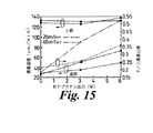
高アスペクト比エッチングを特徴づける基本機構の一つには、エッチング生成物及びエッチング(及び不働態)反応性前駆物質の拡散がある。不働態ステップにおけるこの種の輸送現像を調べた。その結果によれば、深い細長溝の底面への側壁不働態種の輸送は低圧の場合に改善される。プラテン出力の増加もまたこれを改善するものである;図15を参照。グラフは、圧力が減少し、また、rfバイアス出力が増加する時の、細長溝の底面付近での改善された不働態化を示している。このデータは、最初に200μm深さの細長溝をエッチングし、それから、不働態ステップだけを使用し、そして走査型電子顕微鏡により、深さによる側壁不働態の変化を測定することによって得られたものである。このことは、エッチング深さによる不働態の変化を確証し、そして、更に、最適なプロセス条件はエッチング深さと共に変化するという考えを支持している。
【0058】
公知技術を、その様な大アスペクト比のプロセスに対して適用する際の限界を、図16のSEMによって示す。注意すべきことは、この割合に大きな不働態/エッチング比の固定パラメータプロセスは、まだ初期側壁ノッチを生じないが、10μmCD、深さ230μmの細長溝のエッチングに対してこれを示すには、SEM拡大率は十分に高くはないということである。図15に示されている傾向から、望ましい高バイアスrf出力と低圧力の条件の下で運転することにより、プロファイルを幾分改善することができる。しかしながら、固定パラメータプロセスとして、高バイアス出力と低圧力の条件は、イオンエネルギーが増大すると共に、マスク選択度を(>100:1から<20:1へと)著しく劣化させる。急激なパラメータ変化を使用する場合、図17のSEMに示してあるように、対応する急激な側壁変化が生じる。次のパラメータを傾斜化することによって、つまり、プラテン出力を増加、圧力を減少、そして、サイクル時間とガス流量とを増加させることによって、75:1を越える妥当な高い選択度を維持しつつ、好ましい結果が得られる(図18を参照)。ここで、SEMは深さ295μm、12μmCDの細長溝エッチング(25:1のアスペクト比)を示す。この場合のプロセス条件を、図19bに示す。
【0059】
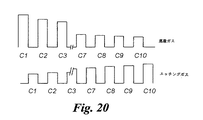
図20は、側壁ノッチを減少させるために、初期サイクルにおいて使用した蒸着ガスとエッチングガスの同期を示す。典型的な動作条件を図19aに与え、そして、それに関わるSEMを図14に示す。図21は、側壁ノッチ減少技術の手法(a)による掃気ガスの使用に関する同期を示す。破線は、代替例として、減少方向に傾斜した掃気ガス流量を示す。
【0060】
図9iは、深い大アスペクト比の異方性エッチングを実現するための同期を示しているが、示されている傾斜化の手法は側壁ノッチの減少にも使用できる。図18に示す結果を得るために、図19bの条件を使用できる。
【0061】
図9iに戻ると、以下のことが分かる:
1. 当該図は、平均圧力の傾斜を示す。サイクルが蒸着からエッチングに変化するそれぞれの場合に、圧力が低圧力から高圧力へと変化することに注意されたい。圧力の下向き傾斜は、エッチングと不働態の両サイクルにおける圧力減少をもたらす。
【0062】
2.当該図は、rfバイアス出力傾斜を示す。バイアスは、サイクルが蒸着からエッチングに変化するそれぞれの場合に、低バイアスから高バイアスへと変化することに注意されたい。これは、上記の圧力変化に同期している。バイアスの上向き傾斜は、この場合、蒸着ステップにのみ当てはまる。
【0063】
3.当該図は、rfバイアス出力傾斜のもう一つの例を示す。ここでもまた、バイアスは、圧力変化に同期して、サイクルが蒸着からエッチングに変化するそれぞれの場合に、低バイアスから高バイアスへと変化する。バイアスの上向き傾斜は、この場合、蒸着ステップとエッチングステップの両方に当てはまる。
【0064】
図9iiは、一般的なパラメータの傾斜を示している。これらの例は、傾斜しているサイクル時間とステップ時間とをそれぞれ示すものである。
【0065】
4.当該図は、サイクル時間傾斜を示す。ここでは、パラメータ(ガス流量、圧力、rf出力等)の大きさが傾斜づけられていない。適用例によっては、これは、上記の場合の“大きさ”の傾斜づけに対する代替形態として使用できるであろう。
【0066】
5.当該図は、サイクル時間傾斜を示す。ここでは、パラメータ(ガス流量、圧力、rf出力等)の大きさも傾斜づけられている。パラメータの傾斜は、大きさに関して増加或いは減少させることができ、減少させる場合、ゼロ或いは非ゼロの値まで減少させることができるということに注意されたい。
【0067】
3.エッチングガス
適切ないずれのエッチングガスも使用できうるが、出願人は、ある特定なガス或いは混合物が有益でありうることを見つけだした。
【0068】
たとえば、プロセス速度に影響するため、エッチング段階においてはいかなる不働態化ガスが含まれることも好ましくないことが引例WO−A−94114187の中に示唆されている。しかしながら、出願人は、この手法により、形成される側壁細長溝の質を大幅に改善することができると結論づけ、そして、O、N、C、炭化水素、ヒドロ−ハロカーボン、及び/或いは、ハロカーボンのような不働態化ガスをエッチングガスに加えうることを提示する。同様に、そして同目的のために、エッチングガスの化学反応性を減少することが望ましく、そして、出願人は、例えば、Cl、Br或いはI等のような、より大きな原子量のハロゲン化物と共にCFxを使用することを提案する。しかしながら、XeF2や他のエッチングガスを使用することもできる。
【0069】
或いは、側壁粗さの度合いは、サイクル時間を制限することによってもまた減少させることができる。例えば、エッチングや蒸着のステップ時間を、7.5秒未満に、好ましくは、5秒未満に制限することが望ましいということが見出された。
【0070】
4.ガリウム砒素と他の材料
以上の提案は、すべて、シリコンにおける細長溝形成についてである。出願人は、適切な不働態化により、ガリウム砒素や、さらにまた、他のエッチング可能な材料の異方性エッチングが達成できることを認めた。例えば、ガリウム砒素へのエッチングは、不働態化ガス或いはエッチング促進ガスを伴っているか、或いは、伴っていないCl2を使ってなしうることが提案できる。しかし、この手法は、一般に、上記に提案した炭素或いは炭化水素不働態を使った場合により大きな成功をもたらしうることが見出された。もし、従来通りのCFx化学物質を使用するなら、エッチング妨害化合物が生成され、そして、それは表面粗さを増大するか或いはエッチングを制限するということになりうる。ガリウム砒素の場合、低圧力かつ高プラズマ密度反応室の使用が考えられるので、低温度が好ましいと考えられる。適切なエッチング化学物質はすでにこの明細書の前段に記載してあるとおりである。
【図面の簡単な説明】
【図1】半導体を処理するための反応室の概略図である。
【図2】公知技術の方法により形成された細長溝の概略図である。
【図3】図2に示されている細長溝の開口部の拡大図である。
【図4】H2に含まれるH4の割合に対するシリコンのエッチング速度を示すプロットである。
【図5】異なる平均イオンエネルギーに対して、H2に含まれるCH4の割合に対するステップカバレッジを示すプロットである。
【図6】ガスと図1の装置の運転パラメータとの間で可能な種々の同期を示すダイアグラムである。
【図7】図6に対する図式であるが、代替的な運転様式を示すものである。
【図8】分圧比に対するシリコンのエッチング速度を示すプロットである。
【図9】(i)は深い異方性プロファイル制御のためのパラメータ傾斜の概略的描写を示す。(ii)は(i)のより一般的な傾斜を示している。
【図10】公知技術に従って形成された細長溝の走査型電子顕微鏡写真がある。
【図11】図10の開口部の拡大図である。
【図12】プロセスパラメータに急激な変化が生じている出願人のプロセスにより形成された細長溝の対応する二つの走査型電子顕微鏡写真である。
【図13】プロセスパラメータに急激な変化が生じている出願人のプロセスにより形成された細長溝の対応する二つの走査型電子顕微鏡写真である。
【図14】傾斜したパラメータが使用されている以外は、図12に対応している。
【図15】種々の反応室圧力におけるRFプラテン出力に対する蒸着速度を示すプロットである。
【図16】公知技術による高アスペクト比の細長溝の走査型電子顕微鏡写真を示す。
【図17】急激な変化を起させる出願人プロセスを使用した場合の図16に対応する走査型電子顕微鏡写真を示す。
【図18】傾斜した変化を使用して、出願人のプロセスにより形成された大アスペクト比細長溝の走査型電子顕微鏡写真である。
【図19】(a)は図14の走査型電子顕微鏡写真により示されている細長溝を形成するために設定されたプロセス条件を示している。(b)は、図18の走査型電子顕微鏡写真により示されている細長溝を形成するために設定されたプロセス条件を示している。
【図20】本発明方法のプロセス初期サイクルの間における蒸着ガス及びエッチングガスの同期を示す図である。
【図21】 排気ガスを使用することによる図20に対する代替的な手法を示す図である。[0001]
TECHNICAL FIELD OF THE INVENTION
The present invention relates to a method for treating a surface of a semiconductor substrate, which does not exclude other methods, but particularly includes a method of depositing a sidewall passivation layer on an etched structure, and a method of passivation. It relates to a method for etching such a structure.
[0002]
[Prior art]
A method of anisotropically etching elongated grooves or depressions in silicon by a method combining etching and vapor deposition is well known. The intention is to perform anisotropic etching while protecting the side walls of the elongated grooves or depressions formed by applying the passivation layer.
[0003]
Such methods are found, for example, in the references US-A-4579623, EP-A-0497023, EP-A-0209951, WO-A-94114187 and US-A-4985114. All of these references describe either the use of a mixture of deposition and etching gases, or the use of alternating etching and deposition steps. The general view is that mixing gases is ineffective. This is because the two processes tend to cancel each other, and in fact there is a prejudice towards using completely alternate steps.
[0004]
Other approaches are described in references EP-A-0383570, U.S. Pat. No. 4,943,344 and U.S. Pat. No. 4,992,136. All of these references seek to keep the substrate at a low temperature, and first of all, less commonly, while etching to remove unwanted deposits from the sidewalls. Utilizes bursts of energetic ions.
[0005]
[Problems to be solved by the invention]
There is a continuing trend in the semiconductor manufacturing industry to require features with higher aspect ratios, which reduce the width of the features and thus increasingly the importance of sidewall profiles and sidewall surface roughness. ing. Currently proposed methods tend to produce rough sidewalls and / or bottom surfaces in the formation and to produce slightly curved or inwardly curved sidewall shapes, depending on the current process. .
[0006]
The manifestation of these various problems depends on the application and the respective process conditions, the exposed silicon area (unmasked substrate area), the etch depth, the aspect ratio, the sidewall profile, and the substrate shape.
[0007]
[Means for Solving the Problems]
The method of the present invention addresses, in at least some embodiments, these various problems and reduces them.
[0008]
In one aspect, the present invention provides a method of etching an elongated groove (by alternating reactive ion etching and passivation layer deposition by chemical vapor deposition) on a semiconductor substrate in a reaction chamber, comprising the following parameters: One or more parameters of gas flow rate, reaction chamber pressure, plasma power, substrate bias, etching rate, deposition rate, cycle time, etching / deposition ratio are changed over time from process cycle to process cycle. The method consists of: The change can be periodic.
[0009]
The etching and vapor deposition steps may overlap, or the etching and vapor deposition gases may be mixed.
[0010]
SaidThe method can include pumping the reaction chamber between the etch and the deposition and / or between the deposition and the etch, wherein:SaidExhaust is the following formula
[0011]
(Equation 2)
Is continued until is satisfied. In the above equation, Ppa is the partial pressure of the gas (A) used in the preceding step, Ppb is the partial pressure of the gas (B) used in the subsequent step, and x is the partial pressure of the process with the gas (A). It represents the rate at which the process speed decreases from a substantially steady state.
[0013]
The gas flow rates for etching and deposition can be changed continuously or rapidly. For example, etching and deposition gases can be provided such that their flow rates are sinusoidal and out of phase. The magnitude of any of these parameters can vary within a cycle and between cycles.
[0014]
Particularly preferably, the deposition rate is increased and / or the etching rate increased, at least during the first cycle, and under suitable conditions, furthermore, for example during the first few cycles from the second to the fourth cycle. Decrease.
[0015]
The etching rates are as follows:
(a) Introduction of scavenging gas
(b) Reduction of plasma power
(c) Reduction of cycle time
(d) Reduction of gas flow
(e) Change in reaction chamber pressure
Can be reduced by one or more of the following:
[0016]
The deposition rates are as follows:
(a) Increase in plasma power
(b) Increase in cycle time
(c) Increasing gas flow
(d) Increasing the density of deposition species
(e) Change in reaction chamber pressure
Can be increased by one or more of the following:
[0017]
Another advantage of this reaction is that the etching and / or deposition steps can have a period of less than 7.5 seconds or even less than 5 seconds to reduce surface roughness; the etching gas is CFxOr XeF2And can include one or more high molecular weight halides to reduce spontaneous etching; and especially, high self-bias (eg, voltage> 20 eV, or even voltage> 100 eV) ) Means that the pressure in the reaction chamber can be reduced and / or the flow rate can be increased during the deposition for shallow and large aspect ratio etching with).
[0018]
In the deposition step, a hydrocarbon deposition gas may be used to deposit a carbon layer or a hydrocarbon layer. The gas may include O, N, or F atoms, and the deposition layer may be doped with nitrogen or fluorine.
[0019]
If back cooling is a problem, the substrate can be placed freely on a support in the reaction chamber. Alternatively, the substrate can be fixed and its temperature can be controlled, for example, to be in the range of -100C to 100C. It may also be advantageous to control the temperature in the reaction chamber to be in the same temperature range as the wafer, so that condensation in the reaction chamber or its equipment is reduced and bottom roughness is reduced.
[0020]
The substrate can be any of GaAs, GaP, GaN, GaSo, SiGe, Mo, W and Ta, wherein the etching gas is particularly preferably accompanied by H or an inert gas, or Unaccompanied Cl2, BCl3, SiCl4, SiCl2H2, CHxCly, CxCly, CHxOne or a combination thereof. Cl2Is particularly preferred. The deposition gas may be one or a combination of CH or CHxCly with or without H or an inert gas. CH4Or CH2Cl2Is particularly preferred.
[0021]
The present invention is as defined above, but it should be construed to include all inventive combinations of the features disclosed above or below.
[0022]
【Example】
The invention can be implemented in various ways. Hereinafter, specific embodiments will be described by way of example with reference to the accompanying drawings.
[0023]
FIG. 1 is a schematic diagram of a
[0024]
The
[0025]
When etching elongated grooves, etching, bias, or other features on the surface of a semiconductor wafer or semiconductor substrate, a typical practice is to deposit a photoresist mask having openings exposing portions of the substrate. I do. Several steps were taken in an effort to ensure that the etching process was downwardly anisotropic in order to incorporate the etching gas into the reaction chamber and to minimize the etching of the sidewalls of the formation as much as possible. Is done. For a variety of reasons, it is practically difficult to achieve a true anisotropic etch, and to deposit a passivating material on the sidewalls so that the material can be sacrificed etched. Various attempts have been made to do so. To date, the most successful such systems are probably those described in reference WO-A-94114187, which systems are shown schematically in FIG. Since the process described in the reference uses a sequential and separate etching and deposition step, after the first etching step, the sidewalls are undercut as shown at 20 and then this undercut is removed by the
[0026]
Applicants propose a series of improvements to the above process to allow for the production of smoother wall formations and, in particular, higher quality, deeper and / or higher aspect ratio formations. For convenience, the description is divided into several items.
[0027]
1. Inactivity
As already mentioned above, prior proposals have deposited a passivation layer in the form of CFx. Applicants propose to passivate the sidewalls using a carbon or hydrocarbon layer. And while those layers provide a fairly high deposition energy, they are particularly noticeable when deposited under high self-bias so that the graphite phase is at least partially removed.
[0028]
If these films or layers are deposited as desired, for example with a high self-bias of 20 eV or more, preferably more than 100 eV, and when it is made for high aspect ratio features, another It has important advantages. This is because a high self-bias ensures that the transport of the deposition material downwardly toward the base of the feature to be etched is increased in order to prevent a recessed sidewall etch. The effect of this transport can be improved by gradually reducing the reaction chamber pressure and / or increasing the gas flow to reduce the residence time. Depending on the configuration, it may be desirable to perform the vapor deposition operation such that a clearly tapered or V-shaped formation is achieved. In the specific example of a shallow (<20 μm) high aspect ratio elongated groove, the opening size (or critical dimension) of the structure may be in the range of <0.5 μm.
[0029]
Hydrocarbon (HC) films formed by this passivation have significant advantages over known fluorocarbon films.
[0030]
For example, the HC film can be easily removed after the etching process is completed by dry ashing (oxygen plasma). This is particularly important in the formation of MEMS (micro-electro-mechanical systems) where wet processing can result in the attachment of resonant structures separated by elongated grooves having a high aspect ratio. For example, in other applications involving optics and biomedical devices, it is essential to completely remove the sidewall layer.
[0031]
The HC film can be made of a wide range of HC precursors (eg, CH containing high molecular weight aromatic HC).4, C2H4, C3H6, C4H8, C2H2Etc.). These are noble gases and / or H2Can be mixed with. An oxygen source gas is also added (eg, CO, CO2, O2Others), which can be used during deposition to control the phase balance of the film. Oxygen is contained in the graphite phase (sp2) To remove the carbon (sp3) Tends to leave a phase. As such, the proportion of oxygen present will affect the properties of the final deposited film or layer.
[0032]
As mentioned above, H2Can be mixed with the HC precursor. H2Etch preferentially etches silicon, and if the proportions are selected correctly, sidewall passivation can be achieved while continuing to etch the bottom of the hole during the passivation phase.
[0033]
A preferred procedure for this is to use a selected HC precursor (eg, CH4) To H2And treating the mask-patterned silicon surface with this mixture in an apparatus used in the proposed etching procedure. Silicon etching rate is H2CH in4Plotted as a function of concentration. An example of such a plot is shown in FIG. It should be noted that the etch rate was CH4Increases from an initial steady state to a peak and then decreases to zero.
[0034]
This graph is considered to indicate that the following mechanism is occurring. In the initial steady state portion, H is used to form the SiHx reaction product.2Activity dominates etching in effect. H2About 10% CH in4Is included, the substrate CH4Etching becomes important (by forming the Si (CHx) y product) and the etching rate increases. Due to the etching, there is no net deposition in this part of the graph, but during this time the deposition of the hydrocarbon layer has taken place. Eventually, this deposition will begin to dominate the etching process and the net deposition will be about 38% CH4Until this continues.
[0035]
It has been found that these changing characteristics can be used in two different ways. If high self-bias or high average ion energy is present (eg, above 100 eV), the applied layer or coating is relatively stiff. Because the coating is much more resistant to etching than the silicon substrate, the reduced graphite phase and process can be manipulated in the rising part of the etch rate graph.sois there. As such, it becomes possible to etch the silicon throughout the deposition phase. Selectivity to mask or resist over 100: 1 can easily be obtained. It should be particularly noted that although there is significant removal of the graphite phase by ion bombardment of the
[0036]
The process may also use only H—C precursors or H2Dilutions can be made and performed. In the latter case, it is preferred to carry out the process in the descending part of the etching graph. That part is CH4Is greater than 18% and less than 38% where net deposition occurs. Generally, the range is CH4Is 18% to 30%.
[0037]
It is believed that lower values of average ion energy during polymer deposition have the advantage of allowing higher mask selectivity. Under these low rf bias conditions, the selectivity is very large over a wide passivation deposition window. Thus, if high selectivity is required, a low average ion energy approach may be advantageous. FIG. 5 shows that CH under the condition range including the above two embodiments.4And
[0038]
Thus, using these techniques, a user can effectively select the combination of etch rate and selectivity that is most appropriate for his proposed structure. Further, enhancement of mask selectivity can be used to increase the etch rate and / or reduce notch formation.
[0039]
FIG. 6 shows how the various parameters of the process are synchronized. FIG. 6 (d) shows the continuous and unchanged coil output, while FIG. 6 (e) switches the coil output to facilitate the etching or deposition step, and the output during etching is It shows that the output differs from that selected for deposition depending on the required process performance. FIG. 6 (e) shows, by way of example, a higher coil output during vapor deposition.
[0040]
6f-i show similar changes in the bias output. FIG. 6 (f) has a high bias output during the etch to facilitate removal of the passivation film, while FIG. 6 (g) has an average with selectivity advantages. 9 illustrates the use of an initial high power pulse to facilitate this removal process while keeping ion energy low. FIG. 6 (h) is a combination of FIGS. 6 (f) and 6 (g) for when higher ion energy is required during etching (eg, a deep elongated groove). FIG. 6 (i) simply shows that the bias can be turned off during the deposition.
[0041]
In some processes, at least the allowable separation time of the gas is determined by the residual partial pressure of gas A (Ppa) that can be tolerated at the partial pressure of gas B (Ppb). This minimum value of Ppa in Ppb is determined as a function of Ppa / (Ppa + Ppb) from the characteristic process rate (etching or deposition).
[0042]
In FIG. 8, gas A is 20% CH.4+ H2And gas B is SF6It is. At Ppa / (Ppa + Ppb) <5%, it can be seen that the process speed is substantially steady. For typical practical conditions, a pump down time of less than 1.5 seconds is sufficient, and the plasma is maintained for 65% of the total cycle time when the process steps are on the order of 2-3 seconds. Also, if the process step exceeds 5 seconds, it can be maintained over 80% of the total cycle time. A suitable synchronization configuration is shown in FIG. It should be noted that it is desirable to avoid mixing gases in the deposition and etching steps, so that etching precedes pumping. Prior art proposals (eg, US Pat. No. 4,985,114) suggest that the deposition gas flow be turned off or reduced for a long time before the plasma is turned on. . This means that the plasma power is only on for a small part of the total cycle time, resulting in a significant decrease in etch rate. Applicants propose that the reaction chamber should be pumped at least during some gas exchanges, but care must be taken to maintain pressure and gas flow stability. Preferably, a mass flow control with a high response speed (rise time <100 ms) and an automatic pressure controller (angle changes to <300 ms and stabilizes) are used.
[0043]
Applicants have shown that pumping time is required to ensure that the etching is not weakened by the deposition gas (see FIG. 8). However, pumping can precede the etching step or both the etching and deposition steps, depending on the details of the process in operation. Also, pumping down reduces micro-loading (as described in U.S. Pat. No. 4,985,114) and is significant for high aspect ratio etching as described below.
[0044]
Many of the parameters that can be varied can be "tilted" as outlined in FIG. 9 (ii). The slope means that the parameters do not change rapidly between cycles, but rather the amplitude or period gradually increases or decreases with each cycle. In the case of pumping down, the slope can be used to allow for mixing at the beginning of the process that can reduce or eliminate sidewall notch formation as described below.
[0045]
Typical process parameters are as follows:
2. Etching / evaporation relationship
Applicants have concluded that the known art approach is inherently too simple. Because during a particular process, it does not change conditions or accept different requirements or different types of formation. Furthermore, the prior art does not address the challenges of deep etching.
[0047]
As such, contrary to what is taught by reference WO-A-94114187, the etching step may be a passivation step or a vapor deposition step so that the surface roughness of the walls is greatly reduced as shown in FIG. Applicants believe that superimposition on steps is often meaningful. Applicants have also concluded that the fixed continuous square wave step used previously is surprisingly far from ideal. In many cases, it is desirable to use a smooth transition between stages, especially between overlapping stages, when a reduction in etch rate is allowed. For this reason, one preferred configuration is to provide a sinusoid with time so that the two "waveforms" are out of phase, preferably close to 90 degrees, for the gas flow rates of the etching gas and the deposition gas. Is to change it. Since sidewall roughness is essentially a manifestation of an increase in the lateral etch component, the sidewall roughness can be reduced by limiting the component of the etch. The desired effect can be achieved in several ways: partially mixing (passing) the passivation and etching steps; minimizing the etching (and thus the corresponding passivation) time; lowering the wafer temperature. Reducing the volatility of the etching product by causing the O, N, C, CFx, and CHx to be added, for example.6, Or a passivation element added to an etching gas, or SF exchanged with CFx or the like.6The etching gas can be obtained by exchanging the etching gas with one of the gases that release a low-reactive species.
[0048]
Applicants have also recognized that changes in etch and deposition levels at different stages in the process are desirable. Applicants propose that during the first cycle or the first few cycles, the deposition time should be increased by increasing the deposition time or rate, or by taking other appropriate measures. Similarly or alternatively, the etch rate or time may be reduced.
[0049]
As already mentioned briefly above, the deeper the formation or elongated groove and / or the higher the aspect ratio, the more difficult it becomes to deposit the material. Good anisotropic etching with appropriate sidewall passivation by controlling the size of one or more of gas flow rate, reaction chamber pressure, plasma power, bias output, cycle time, substrate etching / deposition ratio The system can be tuned in an appropriate manner to achieve
[0050]
These and related approaches can be used to overcome some problems in the etch profile, as follows.
[0051]
a. Side wall notch formation
The problem of sidewall "notching" is particularly sensitive to the size of the exposed silicon area (more severe for low exposed areas of less than 30%), and is equally severe at high silicon average etch rates. Applicants believe that such a notch type is caused by a relatively high concentration of etching species during the initial etch / deposition cycle. As such, the solution adopted by the applicant is to either promote passivation or extinguish the etch species during the first cycle. The latter may be due to process adjustments (grading one or more parameters), or placing substances in the reaction chamber that consume (by chemical reaction) etching species such as Si, Ti, W, etc. that react with the F etchant. Can be achieved either way. Such a chemical load has the disadvantage that it reduces the average etch rate, since the extinction is only required in the first few etching steps. As such, a process conditioning solution is deemed advantageous.
[0052]
It is desirable to reduce / eliminate sidewall notch formation without weakening or degrading any other aspects such as etch rate, profile control, selectivity, and the like. According to the applicant's research'At the start of etchingKickThe concentration of the etching speciesReduceMethodOptimal control ofIsThatprocessTo
a. Introduction of fluorine scavenging gasOr
b. Low coil outputOr
c. Low etching cycle time (step duration)Or
d. Low etching gas flow rateOr
e. Related increase in the above ad parameters during the passivation cycle
f. Combination of the above
BystartThis is then achieved by increasing the (these) individual parameters to, for example, the pre-optimized etching conditions shown in FIG.The increase occurs rapidly (That is,SaidParameters a to fSteppedUse change) or slopePerformbe able to. These two methodsGivesThe resultConventionalThe following is a comparison with the teaching of technology.
[0053]
The essence of the problem (which arises by applying the known technique directly) during the etching of the silicon elongated trench is schematically shown in FIG. 3 and is also illustrated by the SEM (scanning electron microscope) of FIGS. Photo). These figures show that at the initial elongated groove opening of 1.7 μm, the notch width is up to 0.37 μm, while the CD loss is 1.2 μm (70%). Such CD loss values are unsuitable for most applications.
[0054]
However, the notched sidewalls can be corrected by using Applicants' methods (e.g., a-f) that can change the process parameters during the initial etching process cycle. If a sharp step is used to change a process parameter, a sharp transition is created in the sidewall profile. The SEM of FIGS. 12 and 13 illustrate this for different process parameters. In FIG. 12, the change in process parameters is clearly illustrated by the sharp transition of the sidewall profile at the point of change of the parameter (after the 8.5 μm etch depth). (Note that there is no sidewall notch.) FIG. 13 shows another abrupt / step change in process parameters. Here, the sidewall passivation is good enough to produce a sharp profile (and no notch) for the first 2 μm. If poor passivation conditions are applied, it is characterized by changes in sidewall angles and the reappearance of notches.
[0055]
By using the "tilt" parameter approach, notches can be removed while creating a smooth sidewall profile without causing any sharp transitions (see SEM in FIG. 14). This figure shows a 22 μm deep slot etch with a smooth, well-defined profile and no CD loss, while maintaining an etch rate comparable to the large undercut process without tilt. FIG. 19A shows the process conditions used in this case.
[0056]
b. Profile control during deep large aspect ratio etching
The teachings of the prior art are limited to those requiring high aspect ratio (> 10: 1) etching. Although the limitations and solutions for relatively deep etching (> 200 μm) are described here, the discussion is for shallow large aspect ratio etching and also very low, eg, less than 0.5 μm. Even in the case of CD values, it applies equally.
[0057]
One of the basic mechanisms that characterize high aspect ratio etching is the diffusion of etch products and etch (and passivation) reactive precursors. This type of transport development in the passivation step was investigated. The results show that the transport of the sidewall passive species to the bottom of the deep elongated groove is improved at low pressure. Increasing platen power also improves this; see FIG. The graph shows improved passivation near the bottom of the elongated groove as the pressure decreases and the rf bias output increases. This data was obtained by first etching a 200 μm deep elongated groove, then using only the passivation step, and measuring the change in sidewall passivation with depth by scanning electron microscopy. It is. This confirms the change in passivation with etch depth, and further supports the notion that optimal process conditions vary with etch depth.
[0058]
The limitations in applying known techniques to such high aspect ratio processes are illustrated by the SEM of FIG. It should be noted that this fixed-passivity / etch-ratio fixed-parameter process does not yet produce an initial sidewall notch, but to demonstrate this for the etching of a 10 μm CD, 230 μm deep trench, the SEM The enlargement is not high enough. From the trend shown in FIG. 15, it is possible to improve the profile somewhat by operating under the conditions of the desired high bias rf power and low pressure. However, as a fixed parameter process, high bias power and low pressure conditions significantly degrade mask selectivity (from> 100: 1 to <20: 1) as ion energy increases. If a sharp parameter change is used, a corresponding sharp sidewall change occurs, as shown in the SEM of FIG. By ramping the following parameters: increasing platen power, decreasing pressure, and increasing cycle time and gas flow, while maintaining a reasonably high selectivity of over 75: 1, Good results are obtained (see FIG. 18). Here, the SEM indicates a narrow groove etching (25: 1 aspect ratio) with a CD of 295 μm and 12 μm. The process conditions in this case are shown in FIG.
[0059]
FIG. 20 shows the synchronization of the deposition and etching gases used in the initial cycle to reduce the sidewall notch. Typical operating conditions are given in FIG. 19a, and the associated SEM is shown in FIG. FIG. 21 shows the synchronization for the use of scavenging gas according to the technique (a) of the sidewall notch reduction technique. The dashed line indicates, as an alternative, the scavenging gas flow inclined in a decreasing direction.
[0060]
While FIG. 9i shows synchronization to achieve a deep, high aspect ratio anisotropic etch, the slope technique shown can also be used to reduce sidewall notches. The conditions of FIG. 19b can be used to obtain the results shown in FIG.
[0061]
Returning to FIG. 9i, the following can be seen:
1. The figure shows the slope of the mean pressure. Note that in each case when the cycle changes from deposition to etching, the pressure changes from low pressure to high pressure. The downward slope of pressure results in a decrease in pressure in both the etching and passivation cycles.
[0062]
2. The figure shows the rf bias output slope. Note that the bias changes from low bias to high bias each time the cycle changes from deposition to etching. This is synchronous with the above-mentioned pressure change. The upward slope of the bias in this case applies only to the deposition step.
[0063]
3. The figure shows another example of the rf bias output slope. Again, the bias changes from a low bias to a high bias in each case when the cycle changes from deposition to etching, synchronously with the pressure change. The upward slope of the bias in this case applies to both the deposition step and the etching step.
[0064]
FIG. 9ii shows the slope of a general parameter. These examples show sloping cycle time and step time, respectively.
[0065]
4. The figure shows the cycle time ramp. Here, the magnitudes of the parameters (gas flow rate, pressure, rf output, etc.) are not inclined. In some applications, this could be used as an alternative to the "magnitude" ramp in the above case.
[0066]
5. The figure shows the cycle time ramp. Here, the magnitudes of the parameters (gas flow rate, pressure, rf output, etc.) are also inclined. Note that the slope of the parameter can be increased or decreased in magnitude, and if it is decreased, it can be reduced to zero or non-zero values.
[0067]
3. Etching gas
While any suitable etching gas may be used, Applicants have found that certain gases or mixtures can be beneficial.
[0068]
For example, it is suggested in WO-A-94114187 that it is not desirable to include any passivating gas during the etching step because it affects the process speed. However, Applicants have concluded that this approach can greatly improve the quality of the formed side wall elongated grooves, and that O, N, C, hydrocarbons, hydro-halocarbons, and / or halo It is proposed that a passivating gas such as carbon can be added to the etching gas. Similarly, and for the same purpose, it is desirable to reduce the chemical reactivity of the etching gas, and applicants have found that CF with a higher atomic weight halide, such as, for example, Cl, Br or I, etc.xSuggest to use. However, XeF2Alternatively, other etching gases can be used.
[0069]
Alternatively, the degree of sidewall roughness can also be reduced by limiting the cycle time. For example, it has been found desirable to limit the etching and deposition step times to less than 7.5 seconds, and preferably to less than 5 seconds.
[0070]
4. Gallium arsenide and other materials
The above proposals are all about the formation of elongated grooves in silicon. Applicants have recognized that with appropriate passivation, anisotropic etching of gallium arsenide and also other etchable materials can be achieved. For example, etching to gallium arsenide with or without a passivation gas or an etch-promoting gas2Can be suggested using However, it has been found that this approach can generally be more successful when using the above proposed carbon or hydrocarbon passivation. If conventional CFx chemistries are used, etch-interfering compounds are created, which can increase surface roughness or limit etching. In the case of gallium arsenide, use of a low-pressure and high-plasma-density reaction chamber is conceivable. Suitable etching chemistries have already been described earlier in this specification.
[Brief description of the drawings]
FIG. 1 is a schematic view of a reaction chamber for processing a semiconductor.
FIG. 2 is a schematic view of an elongated groove formed by a known technique.
FIG. 3 is an enlarged view of an opening of an elongated groove shown in FIG. 2;
FIG. 4 H2H contained in43 is a plot showing the etching rate of silicon with respect to the ratio of.
FIG. 5: H for different average ion energies2CH included in46 is a plot showing the step coverage with respect to the ratio of.
FIG. 6 is a diagram illustrating the various possible synchronizations between the gas and the operating parameters of the device of FIG. 1;
FIG. 7 is a schematic to FIG. 6, but showing an alternative mode of operation.
FIG. 8 is a plot showing the etching rate of silicon versus the partial pressure ratio.
FIG. 9 (i) shows a schematic depiction of parameter slope for deep anisotropic profile control. (Ii) shows a more general slope of (i).
FIG. 10 is a scanning electron micrograph of an elongated groove formed according to a known technique.
FIG. 11 is an enlarged view of an opening in FIG. 10;
FIG. 12 is two corresponding scanning electron micrographs of an elongated groove formed by Applicants' process where abrupt changes in process parameters have occurred.
FIG. 13 is two corresponding scanning electron micrographs of an elongated groove formed by Applicants' process in which abrupt changes in process parameters have occurred.
FIG. 14 corresponds to FIG. 12, except that a tilted parameter is used.
FIG. 15 is a plot showing deposition rate versus RF platen output at various reaction chamber pressures.
FIG. 16 shows a scanning electron micrograph of a high aspect ratio elongated groove according to the prior art.
FIG. 17 shows a scanning electron micrograph corresponding to FIG. 16 with the use of the abrupt change applicant process.
FIG. 18 is a scanning electron micrograph of a large aspect ratio elongated groove formed by Applicants' process using a ramped change.
FIG. 19 (a) shows the process conditions set for forming the elongated groove shown in the scanning electron micrograph of FIG. (B) shows the process conditions set for forming the elongated grooves shown in the scanning electron micrograph of FIG.
FIG.FIG. 3 illustrates the synchronization of the deposition gas and the etching gas during the initial process cycle of the method of the present invention.
FIG. 21 FIG. 21 illustrates an alternative approach to FIG. 20 by using exhaust gas.
Claims (31)
Ppaが先行プロセスで使用された第一のガスの分圧であり、
Ppbが後続プロセスで使用される第二のガスの分圧であり、
xが、第一のガスが関与する先行プロセスのプロセス速度が実質的定常状態から低下する割合である、
ことを特徴とする請求項7に記載の方法。Pump exhaust
Ppa is the partial pressure of the first gas used in the preceding process;
Ppb is the partial pressure of the second gas used in the subsequent process;
x is the rate at which the process speed of the preceding process involving the first gas decreases from a substantially steady state;
The method of claim 7, wherein:
反応室内で基板に周期的プロセスを実施し、該周期的プロセスが複数の継起プロセスサイクルから成り、該継起プロセスサイクルのそれぞれが反応性イオンエッチングから成る第一のプロセスと化学蒸着による不導態層の蒸着から成る第二のプロセスとを含み、前記周期的プロセスにおける複数のパラメータのうち少なくとも一つをプロセスサイクルからプロセスサイクルへ時間とともに変化させ、
前記周期的プロセスの少なくとも最初のプロセスサイクルの前記第二のプロセスの蒸着速度を、前記周期的プロセスの後続プロセスサイクルの前記第二のプロセスの蒸着速度に比して大きくすることを特徴とする半導体基板の表面処理方法。A method for etching a structure on a semiconductor substrate, comprising:
Performing a periodic process on a substrate in a reaction chamber, wherein the periodic process comprises a plurality of successive process cycles, each of the successive process cycles comprising a reactive ion etch and a passivation layer by chemical vapor deposition. A second process consisting of vapor deposition, wherein at least one of the plurality of parameters in the periodic process is changed over time from a process cycle to a process cycle,
A semiconductor, wherein a deposition rate of the second process in at least an initial process cycle of the periodic process is increased as compared with a deposition rate of the second process in a subsequent process cycle of the periodic process. Substrate surface treatment method.
反応室内で基板に周期的プロセスを実施し、該周期的プロセスが複数の継起プロセスサイクルから成り、該継起プロセスサイクルのそれぞれが反応性イオンエッチングから成る第一のプロセスと化学蒸着による不導態層の蒸着から成る第二のプロセスとを含み、前記周期的プロセスにおける複数のパラメータのうち少なくとも一つをプロセスサイクルからプロセスサイクルへ時間とともに変化させ、
前記周期的プロセスの少なくとも最初のプロセスサイクルの前記第一のプロセスのエッチング速度を前記周期的プロセスの後続プロセスサイクルの前記第一のプロセスのエッチング速度に比して小さくすることを特徴とする半導体基板の表面処理方法。A method for etching a structure on a semiconductor substrate, comprising:
Performing a periodic process on a substrate in a reaction chamber, wherein the periodic process comprises a plurality of successive process cycles, each of the successive process cycles comprising a reactive ion etch and a passivation layer by chemical vapor deposition. A second process consisting of vapor deposition, wherein at least one of the plurality of parameters in the periodic process is changed over time from a process cycle to a process cycle,
A semiconductor substrate, wherein an etching rate of the first process in at least a first process cycle of the periodic process is made smaller than an etching rate of the first process in a subsequent process cycle of the periodic process. Surface treatment method.
反応室内で基板に周期的プロセスを実施し、該周期的プロセスが複数の継起プロセスサイクルから成り、該継起プロセスサイクルのそれぞれが反応性イオンエッチングから成る第一のプロセスと化学蒸着による不導態層の蒸着から成る第二のプロセスとを含み、前記周期的プロセスにおける複数のパラメータのうち少なくとも一つをプロセスサイクルからプロセスサイクルへ時間とともに変化させ、
前記周期的プロセスの少なくとも最初のプロセスサイクルの前記第二のプロセスの蒸着速度を、前記周期的プロセスの後続プロセスサイクルの前記第二のプロセスの蒸着速度に比して大きくし、且つ、前記周期的プロセスの少なくとも最初のプロセスサイクルの前記第一のプロセスのエッチング速度を前記周期的プロセスの後続プロセスサイクルの前記第一のプロセスのエッチング速度に比して小さくすることを特徴とする半導体基板の表面処理方法。A method for etching a structure on a semiconductor substrate, comprising:
Performing a periodic process on a substrate in a reaction chamber, wherein the periodic process comprises a plurality of successive process cycles, each of the successive process cycles comprising a reactive ion etch and a passivation layer by chemical vapor deposition. A second process consisting of vapor deposition, wherein at least one of the plurality of parameters in the periodic process is changed over time from a process cycle to a process cycle,
Increasing the deposition rate of the second process in at least the first process cycle of the periodic process relative to the deposition rate of the second process in a subsequent process cycle of the periodic process; and Surface treatment of a semiconductor substrate, wherein the etching rate of the first process in at least the first process cycle of the process is reduced as compared with the etching rate of the first process in a subsequent process cycle of the periodic process. Method.
Applications Claiming Priority (4)
| Application Number | Priority Date | Filing Date | Title |
|---|---|---|---|
| GBGB9616224.3A GB9616224D0 (en) | 1996-08-01 | 1996-08-01 | Method of surface treatment of semiconductor substrates |
| GB9616224.3 | 1996-08-01 | ||
| GBGB9616223.5A GB9616223D0 (en) | 1996-08-01 | 1996-08-01 | Method of surface treatment of semiconductor substrates |
| GB9616223.5 | 1996-08-01 |
Related Child Applications (1)
| Application Number | Title | Priority Date | Filing Date |
|---|---|---|---|
| JP2003423892A Division JP4550408B2 (en) | 1996-08-01 | 2003-12-19 | Method for surface treatment of semiconductor substrate |
Publications (2)
| Publication Number | Publication Date |
|---|---|
| JPH10135192A JPH10135192A (en) | 1998-05-22 |
| JP3540129B2 true JP3540129B2 (en) | 2004-07-07 |
Family
ID=26309796
Family Applications (2)
| Application Number | Title | Priority Date | Filing Date |
|---|---|---|---|
| JP20667297A Expired - Lifetime JP3540129B2 (en) | 1996-08-01 | 1997-07-31 | Method of surface treatment of semiconductor substrate |
| JP2003423892A Expired - Lifetime JP4550408B2 (en) | 1996-08-01 | 2003-12-19 | Method for surface treatment of semiconductor substrate |
Family Applications After (1)
| Application Number | Title | Priority Date | Filing Date |
|---|---|---|---|
| JP2003423892A Expired - Lifetime JP4550408B2 (en) | 1996-08-01 | 2003-12-19 | Method for surface treatment of semiconductor substrate |
Country Status (5)
| Country | Link |
|---|---|
| US (1) | US6051503A (en) |
| EP (2) | EP0822582B1 (en) |
| JP (2) | JP3540129B2 (en) |
| AT (1) | ATE251341T1 (en) |
| DE (1) | DE69725245T2 (en) |
Cited By (1)
| Publication number | Priority date | Publication date | Assignee | Title |
|---|---|---|---|---|
| JP2018093189A (en) * | 2016-11-30 | 2018-06-14 | 東京エレクトロン株式会社 | Plasma etching method |
Families Citing this family (227)
| Publication number | Priority date | Publication date | Assignee | Title |
|---|---|---|---|---|
| US6849471B2 (en) | 2003-03-28 | 2005-02-01 | Reflectivity, Inc. | Barrier layers for microelectromechanical systems |
| US6969635B2 (en) | 2000-12-07 | 2005-11-29 | Reflectivity, Inc. | Methods for depositing, releasing and packaging micro-electromechanical devices on wafer substrates |
| GB9616225D0 (en) * | 1996-08-01 | 1996-09-11 | Surface Tech Sys Ltd | Method of surface treatment of semiconductor substrates |
| US6749717B1 (en) * | 1997-02-04 | 2004-06-15 | Micron Technology, Inc. | Device for in-situ cleaning of an inductively-coupled plasma chambers |
| DE19736370C2 (en) * | 1997-08-21 | 2001-12-06 | Bosch Gmbh Robert | Process for anisotropic etching of silicon |
| KR100528685B1 (en) * | 1998-03-12 | 2005-11-15 | 가부시끼가이샤 히다치 세이사꾸쇼 | Method for processing surface of sample |
| US6194038B1 (en) | 1998-03-20 | 2001-02-27 | Applied Materials, Inc. | Method for deposition of a conformal layer on a substrate |
| US6642149B2 (en) * | 1998-09-16 | 2003-11-04 | Tokyo Electron Limited | Plasma processing method |
| JP4153606B2 (en) | 1998-10-22 | 2008-09-24 | 東京エレクトロン株式会社 | Plasma etching method and plasma etching apparatus |
| ATE458273T1 (en) * | 1998-11-04 | 2010-03-15 | Surface Technology Systems Plc | METHOD FOR ETCHING A SUBSTRATE |
| JP4714309B2 (en) * | 1998-12-11 | 2011-06-29 | サーフィス テクノロジー システムズ ピーエルシー | Plasma processing equipment |
| US6417013B1 (en) | 1999-01-29 | 2002-07-09 | Plasma-Therm, Inc. | Morphed processing of semiconductor devices |
| GB2348399A (en) * | 1999-03-31 | 2000-10-04 | Univ Glasgow | Reactive ion etching with control of etch gas flow rate, pressure and rf power |
| US6383938B2 (en) * | 1999-04-21 | 2002-05-07 | Alcatel | Method of anisotropic etching of substrates |
| DE19919832A1 (en) * | 1999-04-30 | 2000-11-09 | Bosch Gmbh Robert | Process for anisotropic plasma etching of semiconductors |
| DE19927806A1 (en) | 1999-06-18 | 2001-01-04 | Bosch Gmbh Robert | Device and method for high-rate etching of a substrate with a plasma etching system and device and method for igniting a plasma and regulating up or pulsing the plasma power |
| DE19930188A1 (en) * | 1999-06-30 | 2001-01-04 | Infineon Technologies Ag | Process for producing trenches for storage capacitors of DRAM semiconductor memories |
| US20030015496A1 (en) * | 1999-07-22 | 2003-01-23 | Sujit Sharan | Plasma etching process |
| GB9917305D0 (en) * | 1999-07-23 | 1999-09-22 | Surface Tech Sys Ltd | Method and apparatus for anisotropic etching |
| EP1077475A3 (en) | 1999-08-11 | 2003-04-02 | Applied Materials, Inc. | Method of micromachining a multi-part cavity |
| US6291357B1 (en) | 1999-10-06 | 2001-09-18 | Applied Materials, Inc. | Method and apparatus for etching a substrate with reduced microloading |
| JP2001110784A (en) * | 1999-10-12 | 2001-04-20 | Hitachi Ltd | Apparatus and method for plasma treatment |
| US6949202B1 (en) | 1999-10-26 | 2005-09-27 | Reflectivity, Inc | Apparatus and method for flow of process gas in an ultra-clean environment |
| US7041224B2 (en) | 1999-10-26 | 2006-05-09 | Reflectivity, Inc. | Method for vapor phase etching of silicon |
| US6960305B2 (en) | 1999-10-26 | 2005-11-01 | Reflectivity, Inc | Methods for forming and releasing microelectromechanical structures |
| US6290864B1 (en) | 1999-10-26 | 2001-09-18 | Reflectivity, Inc. | Fluoride gas etching of silicon with improved selectivity |
| US6942811B2 (en) | 1999-10-26 | 2005-09-13 | Reflectivity, Inc | Method for achieving improved selectivity in an etching process |
| US6890863B1 (en) * | 2000-04-27 | 2005-05-10 | Micron Technology, Inc. | Etchant and method of use |
| JP3525862B2 (en) * | 2000-05-22 | 2004-05-10 | トヨタ自動車株式会社 | Sensor element and sensor device |
| US7019376B2 (en) | 2000-08-11 | 2006-03-28 | Reflectivity, Inc | Micromirror array device with a small pitch size |
| EP1311310A4 (en) | 2000-08-21 | 2004-11-24 | Cleveland Clinic Foundation | Microneedle array module and method of fabricating the same |
| US6784108B1 (en) * | 2000-08-31 | 2004-08-31 | Micron Technology, Inc. | Gas pulsing for etch profile control |
| US6402301B1 (en) | 2000-10-27 | 2002-06-11 | Lexmark International, Inc | Ink jet printheads and methods therefor |
| WO2002075801A2 (en) * | 2000-11-07 | 2002-09-26 | Tokyo Electron Limited | Method of fabricating oxides with low defect densities |
| US6743732B1 (en) * | 2001-01-26 | 2004-06-01 | Taiwan Semiconductor Manufacturing Company | Organic low K dielectric etch with NH3 chemistry |
| US6451673B1 (en) * | 2001-02-15 | 2002-09-17 | Advanced Micro Devices, Inc. | Carrier gas modification for preservation of mask layer during plasma etching |
| US20020139771A1 (en) * | 2001-02-22 | 2002-10-03 | Ping Jiang | Gas switching during an etch process to modulate the characteristics of the etch |
| US20020139477A1 (en) * | 2001-03-30 | 2002-10-03 | Lam Research Corporation | Plasma processing method and apparatus with control of plasma excitation power |
| US20020158047A1 (en) * | 2001-04-27 | 2002-10-31 | Yiqiong Wang | Formation of an optical component having smooth sidewalls |
| US20020158046A1 (en) * | 2001-04-27 | 2002-10-31 | Chi Wu | Formation of an optical component |
| US6635556B1 (en) * | 2001-05-17 | 2003-10-21 | Matrix Semiconductor, Inc. | Method of preventing autodoping |
| WO2002095800A2 (en) * | 2001-05-22 | 2002-11-28 | Reflectivity, Inc. | A method for making a micromechanical device by removing a sacrificial layer with multiple sequential etchants |
| US6555166B2 (en) * | 2001-06-29 | 2003-04-29 | International Business Machines | Method for reducing the microloading effect in a chemical vapor deposition reactor |
| US7067849B2 (en) | 2001-07-17 | 2006-06-27 | Lg Electronics Inc. | Diode having high brightness and method thereof |
| US6555480B2 (en) | 2001-07-31 | 2003-04-29 | Hewlett-Packard Development Company, L.P. | Substrate with fluidic channel and method of manufacturing |
| US6890859B1 (en) * | 2001-08-10 | 2005-05-10 | Cypress Semiconductor Corporation | Methods of forming semiconductor structures having reduced defects, and articles and devices formed thereby |
| US7189332B2 (en) | 2001-09-17 | 2007-03-13 | Texas Instruments Incorporated | Apparatus and method for detecting an endpoint in a vapor phase etch |
| WO2003030239A1 (en) * | 2001-09-28 | 2003-04-10 | Sumitomo Precision Products Co., Ltd. | Silicon substrate etching method and etching apparatus |
| US7115516B2 (en) * | 2001-10-09 | 2006-10-03 | Applied Materials, Inc. | Method of depositing a material layer |
| US6949395B2 (en) * | 2001-10-22 | 2005-09-27 | Oriol, Inc. | Method of making diode having reflective layer |
| US7148520B2 (en) | 2001-10-26 | 2006-12-12 | Lg Electronics Inc. | Diode having vertical structure and method of manufacturing the same |
| US6906845B2 (en) * | 2001-11-26 | 2005-06-14 | Samsung Electronics Co., Ltd. | Micro-mechanical device having anti-stiction layer and method of manufacturing the device |
| FR2834382B1 (en) * | 2002-01-03 | 2005-03-18 | Cit Alcatel | METHOD AND DEVICE FOR ANISOTROPIC SILICON ETCHING WITH HIGH ASPECT FACTOR |
| US7027200B2 (en) | 2002-03-22 | 2006-04-11 | Reflectivity, Inc | Etching method used in fabrications of microstructures |
| US6965468B2 (en) | 2003-07-03 | 2005-11-15 | Reflectivity, Inc | Micromirror array having reduced gap between adjacent micromirrors of the micromirror array |
| US6979652B2 (en) * | 2002-04-08 | 2005-12-27 | Applied Materials, Inc. | Etching multi-shaped openings in silicon |
| US6818562B2 (en) | 2002-04-19 | 2004-11-16 | Applied Materials Inc | Method and apparatus for tuning an RF matching network in a plasma enhanced semiconductor wafer processing system |
| US6846746B2 (en) * | 2002-05-01 | 2005-01-25 | Applied Materials, Inc. | Method of smoothing a trench sidewall after a deep trench silicon etch process |
| US6849554B2 (en) | 2002-05-01 | 2005-02-01 | Applied Materials, Inc. | Method of etching a deep trench having a tapered profile in silicon |
| US6759340B2 (en) | 2002-05-09 | 2004-07-06 | Padmapani C. Nallan | Method of etching a trench in a silicon-on-insulator (SOI) structure |
| US6905626B2 (en) * | 2002-07-24 | 2005-06-14 | Unaxis Usa Inc. | Notch-free etching of high aspect SOI structures using alternating deposition and etching and pulsed plasma |
| US7074723B2 (en) * | 2002-08-02 | 2006-07-11 | Applied Materials, Inc. | Method of plasma etching a deeply recessed feature in a substrate using a plasma source gas modulated etchant system |
| US6924235B2 (en) | 2002-08-16 | 2005-08-02 | Unaxis Usa Inc. | Sidewall smoothing in high aspect ratio/deep etching using a discrete gas switching method |
| US6921490B1 (en) | 2002-09-06 | 2005-07-26 | Kotura, Inc. | Optical component having waveguides extending from a common region |
| US6946362B2 (en) * | 2002-09-06 | 2005-09-20 | Hewlett-Packard Development Company, L.P. | Method and apparatus for forming high surface area material films and membranes |
| AU2003275018B2 (en) | 2002-09-20 | 2009-10-01 | Integrated Dna Technologies, Inc. | Anthraquinone quencher dyes, their methods of preparation and use |
| US6902867B2 (en) * | 2002-10-02 | 2005-06-07 | Lexmark International, Inc. | Ink jet printheads and methods therefor |
| US7977390B2 (en) | 2002-10-11 | 2011-07-12 | Lam Research Corporation | Method for plasma etching performance enhancement |
| US7169695B2 (en) * | 2002-10-11 | 2007-01-30 | Lam Research Corporation | Method for forming a dual damascene structure |
| US6833325B2 (en) * | 2002-10-11 | 2004-12-21 | Lam Research Corporation | Method for plasma etching performance enhancement |
| SG152920A1 (en) * | 2002-10-11 | 2009-06-29 | Lam Res Corp | A method for plasma etching performance enhancement |
| DE10247913A1 (en) * | 2002-10-14 | 2004-04-22 | Robert Bosch Gmbh | Process for the anisotropic etching of structures in a substrate arranged in an etching chamber used in semiconductor manufacture comprises using an etching gas and a passivating gas which is fed to the chamber in defined periods |
| US6913942B2 (en) | 2003-03-28 | 2005-07-05 | Reflectvity, Inc | Sacrificial layers for use in fabrications of microelectromechanical devices |
| US7115520B2 (en) * | 2003-04-07 | 2006-10-03 | Unaxis Usa, Inc. | Method and apparatus for process control in time division multiplexed (TDM) etch process |
| US6916746B1 (en) * | 2003-04-09 | 2005-07-12 | Lam Research Corporation | Method for plasma etching using periodic modulation of gas chemistry |
| US7294580B2 (en) * | 2003-04-09 | 2007-11-13 | Lam Research Corporation | Method for plasma stripping using periodic modulation of gas chemistry and hydrocarbon addition |
| DE10318568A1 (en) * | 2003-04-15 | 2004-11-25 | Technische Universität Dresden | Silicon substrate with positive etching profiles with a defined angle of repose and method of production |
| US20040224524A1 (en) * | 2003-05-09 | 2004-11-11 | Applied Materials, Inc. | Maintaining the dimensions of features being etched on a lithographic mask |
| US6980347B2 (en) | 2003-07-03 | 2005-12-27 | Reflectivity, Inc | Micromirror having reduced space between hinge and mirror plate of the micromirror |
| JP4161857B2 (en) * | 2003-09-10 | 2008-10-08 | 株式会社デンソー | Manufacturing method of semiconductor device |
| US7645704B2 (en) | 2003-09-17 | 2010-01-12 | Texas Instruments Incorporated | Methods and apparatus of etch process control in fabrications of microstructures |
| US7135410B2 (en) * | 2003-09-26 | 2006-11-14 | Lam Research Corporation | Etch with ramping |
| US20050112891A1 (en) * | 2003-10-21 | 2005-05-26 | David Johnson | Notch-free etching of high aspect SOI structures using a time division multiplex process and RF bias modulation |
| EP1690290A4 (en) * | 2003-12-04 | 2008-10-22 | Bae Systems Information | Gan-based permeable base transistor and method of fabrication |
| JP3816484B2 (en) | 2003-12-15 | 2006-08-30 | 日本航空電子工業株式会社 | Dry etching method |
| US20050211668A1 (en) * | 2004-03-26 | 2005-09-29 | Lam Research Corporation | Methods of processing a substrate with minimal scalloping |
| JP4416569B2 (en) * | 2004-05-24 | 2010-02-17 | キヤノン株式会社 | Deposited film forming method and deposited film forming apparatus |
| US7053003B2 (en) * | 2004-10-27 | 2006-05-30 | Lam Research Corporation | Photoresist conditioning with hydrogen ramping |
| JP2006173293A (en) * | 2004-12-15 | 2006-06-29 | Toshiba Corp | Method of manufacturing semiconductor device |
| US7459100B2 (en) * | 2004-12-22 | 2008-12-02 | Lam Research Corporation | Methods and apparatus for sequentially alternating among plasma processes in order to optimize a substrate |
| US20060168794A1 (en) * | 2005-01-28 | 2006-08-03 | Hitachi Global Storage Technologies | Method to control mask profile for read sensor definition |
| US20070026682A1 (en) * | 2005-02-10 | 2007-02-01 | Hochberg Michael J | Method for advanced time-multiplexed etching |
| US7491647B2 (en) | 2005-03-08 | 2009-02-17 | Lam Research Corporation | Etch with striation control |
| US7241683B2 (en) | 2005-03-08 | 2007-07-10 | Lam Research Corporation | Stabilized photoresist structure for etching process |
| GB0508706D0 (en) | 2005-04-28 | 2005-06-08 | Oxford Instr Plasma Technology | Method of generating and using a plasma processing control program |
| FR2887073B1 (en) * | 2005-06-14 | 2007-08-10 | Alcatel Sa | METHOD FOR CONTROLLING PRESSURE IN A PROCESS CHAMBER |
| US7425507B2 (en) * | 2005-06-28 | 2008-09-16 | Micron Technology, Inc. | Semiconductor substrates including vias of nonuniform cross section, methods of forming and associated structures |
| JP4707178B2 (en) * | 2005-06-29 | 2011-06-22 | キヤノンマーケティングジャパン株式会社 | Etching method and etching apparatus |
| EP1804281B1 (en) | 2005-12-28 | 2011-12-14 | STMicroelectronics Srl | Process for digging a deep trench in a semiconductor body and semiconductor body so obtained |
| US7910489B2 (en) | 2006-02-17 | 2011-03-22 | Lam Research Corporation | Infinitely selective photoresist mask etch |
| US7341953B2 (en) * | 2006-04-17 | 2008-03-11 | Lam Research Corporation | Mask profile control for controlling feature profile |
| US7829465B2 (en) * | 2006-08-09 | 2010-11-09 | Shouliang Lai | Method for plasma etching of positively sloped structures |
| DE102006043389A1 (en) * | 2006-09-06 | 2008-03-27 | Technische Universität Dresden | Plasma etching process for producing positive etch profiles in silicon substrates |
| US7309646B1 (en) * | 2006-10-10 | 2007-12-18 | Lam Research Corporation | De-fluoridation process |
| JP2008205436A (en) * | 2007-01-26 | 2008-09-04 | Toshiba Corp | Method of manufacturing fine structure |
| US20080239428A1 (en) * | 2007-04-02 | 2008-10-02 | Inphase Technologies, Inc. | Non-ft plane angular filters |
| US7758155B2 (en) * | 2007-05-15 | 2010-07-20 | Eastman Kodak Company | Monolithic printhead with multiple rows of inkjet orifices |
| US20080284835A1 (en) * | 2007-05-15 | 2008-11-20 | Panchawagh Hrishikesh V | Integral, micromachined gutter for inkjet printhead |
| US9123509B2 (en) * | 2007-06-29 | 2015-09-01 | Varian Semiconductor Equipment Associates, Inc. | Techniques for plasma processing a substrate |
| US20090033727A1 (en) * | 2007-07-31 | 2009-02-05 | Anagnostopoulos Constantine N | Lateral flow device printhead with internal gutter |
| US8609546B2 (en) | 2007-11-29 | 2013-12-17 | Lam Research Corporation | Pulsed bias plasma process to control microloading |
| US9059116B2 (en) | 2007-11-29 | 2015-06-16 | Lam Research Corporation | Etch with pulsed bias |
| JP5172417B2 (en) * | 2008-03-27 | 2013-03-27 | Sppテクノロジーズ株式会社 | Manufacturing method of silicon structure, manufacturing apparatus thereof, and manufacturing program thereof |
| US8585179B2 (en) * | 2008-03-28 | 2013-11-19 | Eastman Kodak Company | Fluid flow in microfluidic devices |
| JP5308080B2 (en) * | 2008-06-18 | 2013-10-09 | Sppテクノロジーズ株式会社 | Manufacturing method of silicon structure, manufacturing apparatus thereof, and manufacturing program thereof |
| US8343878B2 (en) * | 2008-12-19 | 2013-01-01 | The Board Of Trustees Of The University Of Illinois | Method of plasma etching GA-based compound semiconductors |
| KR101795658B1 (en) * | 2009-01-31 | 2017-11-08 | 어플라이드 머티어리얼스, 인코포레이티드 | Method and apparatus for etching |
| JP5532394B2 (en) | 2009-10-15 | 2014-06-25 | セイコーエプソン株式会社 | Semiconductor device, circuit board, and electronic equipment |
| CN102135733B (en) * | 2010-01-27 | 2012-12-05 | 中芯国际集成电路制造(上海)有限公司 | Method for removing photoresistance |
| US8384183B2 (en) * | 2010-02-19 | 2013-02-26 | Allegro Microsystems, Inc. | Integrated hall effect element having a germanium hall plate |
| JP5223878B2 (en) | 2010-03-30 | 2013-06-26 | 株式会社デンソー | Manufacturing method of semiconductor device |
| US8642448B2 (en) | 2010-06-22 | 2014-02-04 | Applied Materials, Inc. | Wafer dicing using femtosecond-based laser and plasma etch |
| KR20120000612A (en) * | 2010-06-28 | 2012-01-04 | 삼성전자주식회사 | Method of manufacturing a semiconductor device |
| US8133349B1 (en) | 2010-11-03 | 2012-03-13 | Lam Research Corporation | Rapid and uniform gas switching for a plasma etch process |
| US8802545B2 (en) | 2011-03-14 | 2014-08-12 | Plasma-Therm Llc | Method and apparatus for plasma dicing a semi-conductor wafer |
| US9105705B2 (en) | 2011-03-14 | 2015-08-11 | Plasma-Therm Llc | Method and apparatus for plasma dicing a semi-conductor wafer |
| US8440473B2 (en) | 2011-06-06 | 2013-05-14 | Lam Research Corporation | Use of spectrum to synchronize RF switching with gas switching during etch |
| US8609548B2 (en) * | 2011-06-06 | 2013-12-17 | Lam Research Corporation | Method for providing high etch rate |
| US8759197B2 (en) | 2011-06-15 | 2014-06-24 | Applied Materials, Inc. | Multi-step and asymmetrically shaped laser beam scribing |
| US8557683B2 (en) | 2011-06-15 | 2013-10-15 | Applied Materials, Inc. | Multi-step and asymmetrically shaped laser beam scribing |
| US8507363B2 (en) | 2011-06-15 | 2013-08-13 | Applied Materials, Inc. | Laser and plasma etch wafer dicing using water-soluble die attach film |
| US8703581B2 (en) | 2011-06-15 | 2014-04-22 | Applied Materials, Inc. | Water soluble mask for substrate dicing by laser and plasma etch |
| US9129904B2 (en) | 2011-06-15 | 2015-09-08 | Applied Materials, Inc. | Wafer dicing using pulse train laser with multiple-pulse bursts and plasma etch |
| US9029242B2 (en) | 2011-06-15 | 2015-05-12 | Applied Materials, Inc. | Damage isolation by shaped beam delivery in laser scribing process |
| US8598016B2 (en) * | 2011-06-15 | 2013-12-03 | Applied Materials, Inc. | In-situ deposited mask layer for device singulation by laser scribing and plasma etch |
| US8912077B2 (en) | 2011-06-15 | 2014-12-16 | Applied Materials, Inc. | Hybrid laser and plasma etch wafer dicing using substrate carrier |
| JP5981106B2 (en) * | 2011-07-12 | 2016-08-31 | 東京エレクトロン株式会社 | Plasma etching method |
| JP6040253B2 (en) | 2011-10-20 | 2016-12-07 | シーウェア システムズSi−Ware Systems | Integrated monolithic optical bench including 3D curved optical element and method for manufacturing the same |
| CN102431960A (en) * | 2011-12-07 | 2012-05-02 | 华中科技大学 | Silicon through hole etching method |
| CN103159163B (en) * | 2011-12-19 | 2016-06-08 | 北京北方微电子基地设备工艺研究中心有限责任公司 | Substrate lithographic method and substrate processing equipment |
| GB2499816A (en) | 2012-02-29 | 2013-09-04 | Oxford Instr Nanotechnology Tools Ltd | Controlling deposition and etching in a chamber with fine time control of parameters and gas flow |
| US8946057B2 (en) | 2012-04-24 | 2015-02-03 | Applied Materials, Inc. | Laser and plasma etch wafer dicing using UV-curable adhesive film |
| JP5713043B2 (en) | 2012-05-07 | 2015-05-07 | 株式会社デンソー | Manufacturing method of semiconductor substrate |
| US9048309B2 (en) | 2012-07-10 | 2015-06-02 | Applied Materials, Inc. | Uniform masking for wafer dicing using laser and plasma etch |
| US8859397B2 (en) | 2012-07-13 | 2014-10-14 | Applied Materials, Inc. | Method of coating water soluble mask for laser scribing and plasma etch |
| US8940619B2 (en) | 2012-07-13 | 2015-01-27 | Applied Materials, Inc. | Method of diced wafer transportation |
| CN102832096B (en) * | 2012-09-20 | 2015-11-25 | 中微半导体设备(上海)有限公司 | A kind of gas supply device for vacuum treatment installation and gas supply thereof and changing method |
| US9252057B2 (en) | 2012-10-17 | 2016-02-02 | Applied Materials, Inc. | Laser and plasma etch wafer dicing with partial pre-curing of UV release dicing tape for film frame wafer application |
| US8975162B2 (en) | 2012-12-20 | 2015-03-10 | Applied Materials, Inc. | Wafer dicing from wafer backside |
| US9236305B2 (en) | 2013-01-25 | 2016-01-12 | Applied Materials, Inc. | Wafer dicing with etch chamber shield ring for film frame wafer applications |
| US9018108B2 (en) | 2013-01-25 | 2015-04-28 | Applied Materials, Inc. | Low shrinkage dielectric films |
| US9620379B2 (en) | 2013-03-14 | 2017-04-11 | Applied Materials, Inc. | Multi-layer mask including non-photodefinable laser energy absorbing layer for substrate dicing by laser and plasma etch |
| JP6180824B2 (en) * | 2013-07-02 | 2017-08-16 | 東京エレクトロン株式会社 | Plasma etching method and plasma etching apparatus |
| CN103400800B (en) * | 2013-08-14 | 2015-09-30 | 中微半导体设备(上海)有限公司 | Bosch lithographic method |
| US9105710B2 (en) | 2013-08-30 | 2015-08-11 | Applied Materials, Inc. | Wafer dicing method for improving die packaging quality |
| US9224650B2 (en) | 2013-09-19 | 2015-12-29 | Applied Materials, Inc. | Wafer dicing from wafer backside and front side |
| US9460966B2 (en) | 2013-10-10 | 2016-10-04 | Applied Materials, Inc. | Method and apparatus for dicing wafers having thick passivation polymer layer |
| US9041198B2 (en) | 2013-10-22 | 2015-05-26 | Applied Materials, Inc. | Maskless hybrid laser scribing and plasma etching wafer dicing process |
| US9054050B2 (en) * | 2013-11-06 | 2015-06-09 | Tokyo Electron Limited | Method for deep silicon etching using gas pulsing |
| US9312177B2 (en) | 2013-12-06 | 2016-04-12 | Applied Materials, Inc. | Screen print mask for laser scribe and plasma etch wafer dicing process |
| US9299614B2 (en) | 2013-12-10 | 2016-03-29 | Applied Materials, Inc. | Method and carrier for dicing a wafer |
| US9293304B2 (en) | 2013-12-17 | 2016-03-22 | Applied Materials, Inc. | Plasma thermal shield for heat dissipation in plasma chamber |
| US9299611B2 (en) | 2014-01-29 | 2016-03-29 | Applied Materials, Inc. | Method of wafer dicing using hybrid laser scribing and plasma etch approach with mask plasma treatment for improved mask etch resistance |
| US9018079B1 (en) | 2014-01-29 | 2015-04-28 | Applied Materials, Inc. | Wafer dicing using hybrid laser scribing and plasma etch approach with intermediate reactive post mask-opening clean |
| US9236284B2 (en) | 2014-01-31 | 2016-01-12 | Applied Materials, Inc. | Cooled tape frame lift and low contact shadow ring for plasma heat isolation |
| US8991329B1 (en) | 2014-01-31 | 2015-03-31 | Applied Materials, Inc. | Wafer coating |
| JP6158111B2 (en) * | 2014-02-12 | 2017-07-05 | 東京エレクトロン株式会社 | Gas supply method and semiconductor manufacturing apparatus |
| US9275902B2 (en) | 2014-03-26 | 2016-03-01 | Applied Materials, Inc. | Dicing processes for thin wafers with bumps on wafer backside |
| US9076860B1 (en) | 2014-04-04 | 2015-07-07 | Applied Materials, Inc. | Residue removal from singulated die sidewall |
| CN103950887B (en) * | 2014-04-09 | 2016-01-20 | 华中科技大学 | A kind of dark silicon etching method |
| US8975163B1 (en) | 2014-04-10 | 2015-03-10 | Applied Materials, Inc. | Laser-dominated laser scribing and plasma etch hybrid wafer dicing |
| US8932939B1 (en) | 2014-04-14 | 2015-01-13 | Applied Materials, Inc. | Water soluble mask formation by dry film lamination |
| US8912078B1 (en) | 2014-04-16 | 2014-12-16 | Applied Materials, Inc. | Dicing wafers having solder bumps on wafer backside |
| US8999816B1 (en) | 2014-04-18 | 2015-04-07 | Applied Materials, Inc. | Pre-patterned dry laminate mask for wafer dicing processes |
| US9159621B1 (en) | 2014-04-29 | 2015-10-13 | Applied Materials, Inc. | Dicing tape protection for wafer dicing using laser scribe process |
| US8912075B1 (en) | 2014-04-29 | 2014-12-16 | Applied Materials, Inc. | Wafer edge warp supression for thin wafer supported by tape frame |
| US9711365B2 (en) | 2014-05-02 | 2017-07-18 | International Business Machines Corporation | Etch rate enhancement for a silicon etch process through etch chamber pretreatment |
| US8980727B1 (en) | 2014-05-07 | 2015-03-17 | Applied Materials, Inc. | Substrate patterning using hybrid laser scribing and plasma etching processing schemes |
| US9112050B1 (en) | 2014-05-13 | 2015-08-18 | Applied Materials, Inc. | Dicing tape thermal management by wafer frame support ring cooling during plasma dicing |
| US9034771B1 (en) | 2014-05-23 | 2015-05-19 | Applied Materials, Inc. | Cooling pedestal for dicing tape thermal management during plasma dicing |
| US9142459B1 (en) | 2014-06-30 | 2015-09-22 | Applied Materials, Inc. | Wafer dicing using hybrid laser scribing and plasma etch approach with mask application by vacuum lamination |
| US9165832B1 (en) | 2014-06-30 | 2015-10-20 | Applied Materials, Inc. | Method of die singulation using laser ablation and induction of internal defects with a laser |
| US9093518B1 (en) | 2014-06-30 | 2015-07-28 | Applied Materials, Inc. | Singulation of wafers having wafer-level underfill |
| US9130057B1 (en) | 2014-06-30 | 2015-09-08 | Applied Materials, Inc. | Hybrid dicing process using a blade and laser |
| US9349648B2 (en) | 2014-07-22 | 2016-05-24 | Applied Materials, Inc. | Hybrid wafer dicing approach using a rectangular shaped two-dimensional top hat laser beam profile or a linear shaped one-dimensional top hat laser beam profile laser scribing process and plasma etch process |
| US9196498B1 (en) | 2014-08-12 | 2015-11-24 | Applied Materials, Inc. | Stationary actively-cooled shadow ring for heat dissipation in plasma chamber |
| US9117868B1 (en) | 2014-08-12 | 2015-08-25 | Applied Materials, Inc. | Bipolar electrostatic chuck for dicing tape thermal management during plasma dicing |
| US9281244B1 (en) | 2014-09-18 | 2016-03-08 | Applied Materials, Inc. | Hybrid wafer dicing approach using an adaptive optics-controlled laser scribing process and plasma etch process |
| US11195756B2 (en) | 2014-09-19 | 2021-12-07 | Applied Materials, Inc. | Proximity contact cover ring for plasma dicing |
| US9177861B1 (en) | 2014-09-19 | 2015-11-03 | Applied Materials, Inc. | Hybrid wafer dicing approach using laser scribing process based on an elliptical laser beam profile or a spatio-temporal controlled laser beam profile |
| US9196536B1 (en) | 2014-09-25 | 2015-11-24 | Applied Materials, Inc. | Hybrid wafer dicing approach using a phase modulated laser beam profile laser scribing process and plasma etch process |
| US9130056B1 (en) | 2014-10-03 | 2015-09-08 | Applied Materials, Inc. | Bi-layer wafer-level underfill mask for wafer dicing and approaches for performing wafer dicing |
| DE102014114613B4 (en) | 2014-10-08 | 2023-10-12 | OSRAM Opto Semiconductors Gesellschaft mit beschränkter Haftung | Radiation-emitting semiconductor chip, method for producing a large number of radiation-emitting semiconductor chips and optoelectronic component with a radiation-emitting semiconductor chip |
| US9245803B1 (en) | 2014-10-17 | 2016-01-26 | Applied Materials, Inc. | Hybrid wafer dicing approach using a bessel beam shaper laser scribing process and plasma etch process |
| US10692765B2 (en) | 2014-11-07 | 2020-06-23 | Applied Materials, Inc. | Transfer arm for film frame substrate handling during plasma singulation of wafers |
| GB201420935D0 (en) | 2014-11-25 | 2015-01-07 | Spts Technologies Ltd | Plasma etching apparatus |
| CN104465336B (en) * | 2014-12-02 | 2017-05-17 | 国家纳米科学中心 | Low-frequency BOSCH deep silicon etching method |
| US9330977B1 (en) | 2015-01-05 | 2016-05-03 | Applied Materials, Inc. | Hybrid wafer dicing approach using a galvo scanner and linear stage hybrid motion laser scribing process and plasma etch process |
| US9159624B1 (en) | 2015-01-05 | 2015-10-13 | Applied Materials, Inc. | Vacuum lamination of polymeric dry films for wafer dicing using hybrid laser scribing and plasma etch approach |
| US9355907B1 (en) | 2015-01-05 | 2016-05-31 | Applied Materials, Inc. | Hybrid wafer dicing approach using a line shaped laser beam profile laser scribing process and plasma etch process |
| US9601375B2 (en) | 2015-04-27 | 2017-03-21 | Applied Materials, Inc. | UV-cure pre-treatment of carrier film for wafer dicing using hybrid laser scribing and plasma etch approach |
| US9478455B1 (en) | 2015-06-12 | 2016-10-25 | Applied Materials, Inc. | Thermal pyrolytic graphite shadow ring assembly for heat dissipation in plasma chamber |
| US9721839B2 (en) | 2015-06-12 | 2017-08-01 | Applied Materials, Inc. | Etch-resistant water soluble mask for hybrid wafer dicing using laser scribing and plasma etch |
| US9691625B2 (en) * | 2015-11-04 | 2017-06-27 | Lam Research Corporation | Methods and systems for plasma etching using bi-modal process gas composition responsive to plasma power level |
| US9972575B2 (en) | 2016-03-03 | 2018-05-15 | Applied Materials, Inc. | Hybrid wafer dicing approach using a split beam laser scribing process and plasma etch process |
| US9852997B2 (en) | 2016-03-25 | 2017-12-26 | Applied Materials, Inc. | Hybrid wafer dicing approach using a rotating beam laser scribing process and plasma etch process |
| US9793132B1 (en) | 2016-05-13 | 2017-10-17 | Applied Materials, Inc. | Etch mask for hybrid laser scribing and plasma etch wafer singulation process |
| GB201608926D0 (en) | 2016-05-20 | 2016-07-06 | Spts Technologies Ltd | Method for plasma etching a workpiece |
| JP2018110156A (en) | 2016-12-28 | 2018-07-12 | キヤノン株式会社 | Semiconductor device, manufacturing method thereof, and camera |
| US11158540B2 (en) | 2017-05-26 | 2021-10-26 | Applied Materials, Inc. | Light-absorbing mask for hybrid laser scribing and plasma etch wafer singulation process |
| US10363629B2 (en) | 2017-06-01 | 2019-07-30 | Applied Materials, Inc. | Mitigation of particle contamination for wafer dicing processes |
| US10535561B2 (en) | 2018-03-12 | 2020-01-14 | Applied Materials, Inc. | Hybrid wafer dicing approach using a multiple pass laser scribing process and plasma etch process |
| GB201810387D0 (en) | 2018-06-25 | 2018-08-08 | Spts Technologies Ltd | Method of plasma etching |
| JP2020009840A (en) * | 2018-07-04 | 2020-01-16 | 東京エレクトロン株式会社 | Etching method and substrate processing apparatus |
| JP2020021765A (en) * | 2018-07-30 | 2020-02-06 | 株式会社アルバック | Manufacturing method of semiconductor element |
| US11355394B2 (en) | 2018-09-13 | 2022-06-07 | Applied Materials, Inc. | Wafer dicing using hybrid laser scribing and plasma etch approach with intermediate breakthrough treatment |
| DE102019116019A1 (en) * | 2019-06-12 | 2020-12-17 | X-Fab Semiconductor Foundries Gmbh | Production of components in substrates via a multi-stage etching process |
| US11011424B2 (en) | 2019-08-06 | 2021-05-18 | Applied Materials, Inc. | Hybrid wafer dicing approach using a spatially multi-focused laser beam laser scribing process and plasma etch process |
| US11342226B2 (en) | 2019-08-13 | 2022-05-24 | Applied Materials, Inc. | Hybrid wafer dicing approach using an actively-focused laser beam laser scribing process and plasma etch process |
| US10903121B1 (en) | 2019-08-14 | 2021-01-26 | Applied Materials, Inc. | Hybrid wafer dicing approach using a uniform rotating beam laser scribing process and plasma etch process |
| US20210118734A1 (en) * | 2019-10-22 | 2021-04-22 | Semiconductor Components Industries, Llc | Plasma-singulated, contaminant-reduced semiconductor die |
| US11600492B2 (en) | 2019-12-10 | 2023-03-07 | Applied Materials, Inc. | Electrostatic chuck with reduced current leakage for hybrid laser scribing and plasma etch wafer singulation process |
| US11177137B2 (en) * | 2020-01-17 | 2021-11-16 | Taiwan Semiconductor Manufacturing Company, Ltd. | Wafer etching process and methods thereof |
| CN111257596B (en) * | 2020-02-25 | 2021-09-14 | 西南交通大学 | Scanning probe microscope narrow and small experiment chamber environment atmosphere accurate control device |
| US11373877B2 (en) | 2020-04-13 | 2022-06-28 | Applied Materials, Inc. | Methods and apparatus for in-situ protection liners for high aspect ratio reactive ion etching |
| US11262506B1 (en) * | 2020-08-07 | 2022-03-01 | Advanced Semiconductor Engineering, Inc. | Recessed portion in a substrate and method of forming the same |
| CN113140455A (en) * | 2021-04-14 | 2021-07-20 | 北京北方华创微电子装备有限公司 | Etching method of inclined through hole |
Family Cites Families (29)
| Publication number | Priority date | Publication date | Assignee | Title |
|---|---|---|---|---|
| EP0048175B1 (en) * | 1980-09-17 | 1986-04-23 | Hitachi, Ltd. | Semiconductor device and method of manufacturing the same |
| JPS6050923A (en) * | 1983-08-31 | 1985-03-22 | Hitachi Ltd | Method of plasma surface treatment and device therefor |
| US4599135A (en) * | 1983-09-30 | 1986-07-08 | Hitachi, Ltd. | Thin film deposition |
| US4533430A (en) * | 1984-01-04 | 1985-08-06 | Advanced Micro Devices, Inc. | Process for forming slots having near vertical sidewalls at their upper extremities |
| US4512841A (en) * | 1984-04-02 | 1985-04-23 | International Business Machines Corporation | RF Coupling techniques |
| US4855017A (en) * | 1985-05-03 | 1989-08-08 | Texas Instruments Incorporated | Trench etch process for a single-wafer RIE dry etch reactor |
| US4784720A (en) * | 1985-05-03 | 1988-11-15 | Texas Instruments Incorporated | Trench etch process for a single-wafer RIE dry etch reactor |
| JPS62502646A (en) * | 1985-09-27 | 1987-10-08 | バロ−ス・コ−ポレ−シヨン | How to create tapered via holes in polyimide |
| JPS62136066A (en) * | 1985-12-09 | 1987-06-19 | Mitsubishi Electric Corp | Manufacture of semiconductor device |
| EP0246514A3 (en) * | 1986-05-16 | 1989-09-20 | Air Products And Chemicals, Inc. | Deep trench etching of single crystal silicon |
| JP2502536B2 (en) * | 1986-08-08 | 1996-05-29 | 松下電器産業株式会社 | Pattern formation method |
| KR900007687B1 (en) * | 1986-10-17 | 1990-10-18 | 가부시기가이샤 히다찌세이사꾸쇼 | Method and device for plasma processing |
| US4707218A (en) * | 1986-10-28 | 1987-11-17 | International Business Machines Corporation | Lithographic image size reduction |
| NL8701867A (en) * | 1987-08-07 | 1989-03-01 | Cobrain Nv | METHOD FOR TREATING, IN PARTICULAR DRY ETCHING OF A SUBSTRATE AND ETCHING DEVICE |
| US5007982A (en) * | 1988-07-11 | 1991-04-16 | North American Philips Corporation | Reactive ion etching of silicon with hydrogen bromide |
| JP2918892B2 (en) * | 1988-10-14 | 1999-07-12 | 株式会社日立製作所 | Plasma etching method |
| IT1225636B (en) * | 1988-12-15 | 1990-11-22 | Sgs Thomson Microelectronics | EXCAVATION METHOD WITH ROUNDED BOTTOM PROFILE FOR INSULATION STRUCTURES BUILT IN SILICON |
| KR900013595A (en) * | 1989-02-15 | 1990-09-06 | 미다 가쓰시게 | Plasma Etching Method and Apparatus |
| JPH03126222A (en) * | 1989-10-12 | 1991-05-29 | Canon Inc | Deposited-film forming method |
| JPH03129820A (en) * | 1989-10-16 | 1991-06-03 | Seiko Epson Corp | Apparatus for manufacturing semiconductor and manufacture of semiconductor device |
| KR910010516A (en) * | 1989-11-15 | 1991-06-29 | 아오이 죠이치 | Semiconductor memory device |
| US5474650A (en) * | 1991-04-04 | 1995-12-12 | Hitachi, Ltd. | Method and apparatus for dry etching |
| JP2913936B2 (en) * | 1991-10-08 | 1999-06-28 | 日本電気株式会社 | Method for manufacturing semiconductor device |
| US5368685A (en) * | 1992-03-24 | 1994-11-29 | Hitachi, Ltd. | Dry etching apparatus and method |
| JP2661455B2 (en) * | 1992-03-27 | 1997-10-08 | 株式会社日立製作所 | Vacuum processing equipment |
| JPH0612767A (en) * | 1992-06-25 | 1994-01-21 | Victor Co Of Japan Ltd | Device for automatic reproducing |
| DE4241045C1 (en) * | 1992-12-05 | 1994-05-26 | Bosch Gmbh Robert | Process for anisotropic etching of silicon |
| JPH07226397A (en) * | 1994-02-10 | 1995-08-22 | Tokyo Electron Ltd | Etching treatment method |
| US5605600A (en) * | 1995-03-13 | 1997-02-25 | International Business Machines Corporation | Etch profile shaping through wafer temperature control |
-
1997
- 1997-07-28 EP EP97305642A patent/EP0822582B1/en not_active Expired - Lifetime
- 1997-07-28 EP EP03013020A patent/EP1357584A3/en not_active Withdrawn
- 1997-07-28 AT AT97305642T patent/ATE251341T1/en not_active IP Right Cessation
- 1997-07-28 DE DE69725245T patent/DE69725245T2/en not_active Expired - Lifetime
- 1997-07-31 JP JP20667297A patent/JP3540129B2/en not_active Expired - Lifetime
- 1997-08-01 US US08/904,953 patent/US6051503A/en not_active Expired - Lifetime
-
2003
- 2003-12-19 JP JP2003423892A patent/JP4550408B2/en not_active Expired - Lifetime
Cited By (2)
| Publication number | Priority date | Publication date | Assignee | Title |
|---|---|---|---|---|
| JP2018093189A (en) * | 2016-11-30 | 2018-06-14 | 東京エレクトロン株式会社 | Plasma etching method |
| JP7008474B2 (en) | 2016-11-30 | 2022-01-25 | 東京エレクトロン株式会社 | Plasma etching method |
Also Published As
| Publication number | Publication date |
|---|---|
| EP0822582B1 (en) | 2003-10-01 |
| ATE251341T1 (en) | 2003-10-15 |
| EP1357584A3 (en) | 2005-01-12 |
| EP1357584A2 (en) | 2003-10-29 |
| DE69725245D1 (en) | 2003-11-06 |
| JP4550408B2 (en) | 2010-09-22 |
| EP0822582A3 (en) | 1998-05-13 |
| US6051503A (en) | 2000-04-18 |
| JPH10135192A (en) | 1998-05-22 |
| JP2004119994A (en) | 2004-04-15 |
| DE69725245T2 (en) | 2004-08-12 |
| EP0822582A2 (en) | 1998-02-04 |
Similar Documents
| Publication | Publication Date | Title |
|---|---|---|
| JP3540129B2 (en) | Method of surface treatment of semiconductor substrate | |
| JP4237281B2 (en) | Semiconductor substrate surface treatment method | |
| US7153779B2 (en) | Method to eliminate striations and surface roughness caused by dry etch | |
| JP4601113B2 (en) | Anisotropic etching method for substrates | |
| JP6352771B2 (en) | Method for trimming carbon-containing films with reduced trimming rate | |
| JP4852196B2 (en) | Method for etching a silicon layer in a plasma processing chamber to form a deep opening | |
| US5413670A (en) | Method for plasma etching or cleaning with diluted NF3 | |
| JP2915807B2 (en) | Etching of molybdenum silicide using sulfur hexafluoride, hydrogen bromide and oxygen | |
| RU2339115C2 (en) | Plasma etching method with usage of intermittent modulation of gaseous reagent | |
| EP1420438A2 (en) | Method and apparatus for etching a deep trench | |
| JPH05275392A (en) | Etching of sio2 film | |
| Chabloz et al. | Improvement of sidewall roughness in deep silicon etching | |
| US20210050222A1 (en) | Plasma etching method | |
| JP4065213B2 (en) | Silicon substrate etching method and etching apparatus | |
| EP2022106A2 (en) | Methods for minimizing mask undercuts and notches for plasma processing system | |
| US5618379A (en) | Selective deposition process | |
| JPH11195641A (en) | Plasma treatment | |
| JPS63292628A (en) | Semiconductor etching for forming oriented inclined wall | |
| US6828251B2 (en) | Method for improved plasma etching control | |
| JPH02156529A (en) | Oxide layer inclined etching method of semiconductor wafer | |
| JP3830560B2 (en) | Dry etching method | |
| JP3363782B2 (en) | Highly selective oxide etching process for integrated circuit structures | |
| JPH06163474A (en) | Dry etching method | |
| JPH0794482A (en) | Dry etching method | |
| JPS6345469B2 (en) |
Legal Events
| Date | Code | Title | Description |
|---|---|---|---|
| A521 | Request for written amendment filed |
Free format text: JAPANESE INTERMEDIATE CODE: A523 Effective date: 20031219 |
|
| A911 | Transfer to examiner for re-examination before appeal (zenchi) |
Free format text: JAPANESE INTERMEDIATE CODE: A911 Effective date: 20040113 |
|
| TRDD | Decision of grant or rejection written | ||
| A01 | Written decision to grant a patent or to grant a registration (utility model) |
Free format text: JAPANESE INTERMEDIATE CODE: A01 Effective date: 20040310 |
|
| A61 | First payment of annual fees (during grant procedure) |
Free format text: JAPANESE INTERMEDIATE CODE: A61 Effective date: 20040324 |
|
| R150 | Certificate of patent or registration of utility model |
Free format text: JAPANESE INTERMEDIATE CODE: R150 |
|
| S111 | Request for change of ownership or part of ownership |
Free format text: JAPANESE INTERMEDIATE CODE: R313113 |
|
| R350 | Written notification of registration of transfer |
Free format text: JAPANESE INTERMEDIATE CODE: R350 |
|
| FPAY | Renewal fee payment (event date is renewal date of database) |
Free format text: PAYMENT UNTIL: 20080402 Year of fee payment: 4 |
|
| FPAY | Renewal fee payment (event date is renewal date of database) |
Free format text: PAYMENT UNTIL: 20080402 Year of fee payment: 4 |
|
| FPAY | Renewal fee payment (event date is renewal date of database) |
Free format text: PAYMENT UNTIL: 20090402 Year of fee payment: 5 |
|
| FPAY | Renewal fee payment (event date is renewal date of database) |
Free format text: PAYMENT UNTIL: 20100402 Year of fee payment: 6 |
|
| FPAY | Renewal fee payment (event date is renewal date of database) |
Free format text: PAYMENT UNTIL: 20110402 Year of fee payment: 7 |
|
| FPAY | Renewal fee payment (event date is renewal date of database) |
Free format text: PAYMENT UNTIL: 20120402 Year of fee payment: 8 |
|
| FPAY | Renewal fee payment (event date is renewal date of database) |
Free format text: PAYMENT UNTIL: 20130402 Year of fee payment: 9 |
|
| FPAY | Renewal fee payment (event date is renewal date of database) |
Free format text: PAYMENT UNTIL: 20140402 Year of fee payment: 10 |
|
| R250 | Receipt of annual fees |
Free format text: JAPANESE INTERMEDIATE CODE: R250 |
|
| R250 | Receipt of annual fees |
Free format text: JAPANESE INTERMEDIATE CODE: R250 |
|
| R250 | Receipt of annual fees |
Free format text: JAPANESE INTERMEDIATE CODE: R250 |
|
| R250 | Receipt of annual fees |
Free format text: JAPANESE INTERMEDIATE CODE: R250 |
|
| EXPY | Cancellation because of completion of term |