JP4153606B2 - Plasma etching method and plasma etching apparatus - Google Patents
Plasma etching method and plasma etching apparatus Download PDFInfo
- Publication number
- JP4153606B2 JP4153606B2 JP31994298A JP31994298A JP4153606B2 JP 4153606 B2 JP4153606 B2 JP 4153606B2 JP 31994298 A JP31994298 A JP 31994298A JP 31994298 A JP31994298 A JP 31994298A JP 4153606 B2 JP4153606 B2 JP 4153606B2
- Authority
- JP
- Japan
- Prior art keywords
- etching
- bias power
- film
- plasma
- processing chamber
- Prior art date
- Legal status (The legal status is an assumption and is not a legal conclusion. Google has not performed a legal analysis and makes no representation as to the accuracy of the status listed.)
- Expired - Lifetime
Links
- 238000000034 method Methods 0.000 title claims description 100
- 238000001020 plasma etching Methods 0.000 title claims description 23
- 238000005530 etching Methods 0.000 claims description 110
- 230000008569 process Effects 0.000 claims description 78
- 238000012545 processing Methods 0.000 claims description 45
- 230000015572 biosynthetic process Effects 0.000 claims description 16
- 230000001681 protective effect Effects 0.000 claims description 16
- VYPSYNLAJGMNEJ-UHFFFAOYSA-N Silicium dioxide Chemical group O=[Si]=O VYPSYNLAJGMNEJ-UHFFFAOYSA-N 0.000 claims description 3
- 230000009467 reduction Effects 0.000 claims description 3
- 229910052814 silicon oxide Inorganic materials 0.000 claims description 3
- NBVXSUQYWXRMNV-UHFFFAOYSA-N fluoromethane Chemical compound FC NBVXSUQYWXRMNV-UHFFFAOYSA-N 0.000 claims description 2
- 229920002120 photoresistant polymer Polymers 0.000 description 50
- 229920000642 polymer Polymers 0.000 description 36
- 150000002500 ions Chemical class 0.000 description 8
- 229910004298 SiO 2 Inorganic materials 0.000 description 7
- 238000000151 deposition Methods 0.000 description 4
- 230000001965 increasing effect Effects 0.000 description 4
- 230000008021 deposition Effects 0.000 description 3
- 238000010586 diagram Methods 0.000 description 3
- 230000000694 effects Effects 0.000 description 3
- BOTDANWDWHJENH-UHFFFAOYSA-N Tetraethyl orthosilicate Chemical compound CCO[Si](OCC)(OCC)OCC BOTDANWDWHJENH-UHFFFAOYSA-N 0.000 description 2
- 238000005520 cutting process Methods 0.000 description 2
- 230000007423 decrease Effects 0.000 description 2
- 238000005137 deposition process Methods 0.000 description 2
- 238000012986 modification Methods 0.000 description 2
- 230000004048 modification Effects 0.000 description 2
- 229910020177 SiOF Inorganic materials 0.000 description 1
- 230000000903 blocking effect Effects 0.000 description 1
- 239000007795 chemical reaction product Substances 0.000 description 1
- 230000008878 coupling Effects 0.000 description 1
- 238000010168 coupling process Methods 0.000 description 1
- 238000005859 coupling reaction Methods 0.000 description 1
- 230000003247 decreasing effect Effects 0.000 description 1
- 238000010494 dissociation reaction Methods 0.000 description 1
- 230000005593 dissociations Effects 0.000 description 1
- 239000011521 glass Substances 0.000 description 1
- 230000001939 inductive effect Effects 0.000 description 1
- 239000002184 metal Substances 0.000 description 1
- 229910052751 metal Inorganic materials 0.000 description 1
- 239000000203 mixture Substances 0.000 description 1
- 239000002245 particle Substances 0.000 description 1
- 239000005360 phosphosilicate glass Substances 0.000 description 1
- 238000012805 post-processing Methods 0.000 description 1
- 238000010791 quenching Methods 0.000 description 1
- 230000000171 quenching effect Effects 0.000 description 1
- 230000007261 regionalization Effects 0.000 description 1
- 239000004065 semiconductor Substances 0.000 description 1
- 238000004904 shortening Methods 0.000 description 1
- 239000000758 substrate Substances 0.000 description 1
Images


Classifications
-
- H—ELECTRICITY
- H01—ELECTRIC ELEMENTS
- H01L—SEMICONDUCTOR DEVICES NOT COVERED BY CLASS H10
- H01L21/00—Processes or apparatus adapted for the manufacture or treatment of semiconductor or solid state devices or of parts thereof
- H01L21/02—Manufacture or treatment of semiconductor devices or of parts thereof
- H01L21/04—Manufacture or treatment of semiconductor devices or of parts thereof the devices having potential barriers, e.g. a PN junction, depletion layer or carrier concentration layer
- H01L21/18—Manufacture or treatment of semiconductor devices or of parts thereof the devices having potential barriers, e.g. a PN junction, depletion layer or carrier concentration layer the devices having semiconductor bodies comprising elements of Group IV of the Periodic Table or AIIIBV compounds with or without impurities, e.g. doping materials
- H01L21/30—Treatment of semiconductor bodies using processes or apparatus not provided for in groups H01L21/20 - H01L21/26
- H01L21/302—Treatment of semiconductor bodies using processes or apparatus not provided for in groups H01L21/20 - H01L21/26 to change their surface-physical characteristics or shape, e.g. etching, polishing, cutting
- H01L21/306—Chemical or electrical treatment, e.g. electrolytic etching
- H01L21/3065—Plasma etching; Reactive-ion etching
-
- H—ELECTRICITY
- H01—ELECTRIC ELEMENTS
- H01J—ELECTRIC DISCHARGE TUBES OR DISCHARGE LAMPS
- H01J37/00—Discharge tubes with provision for introducing objects or material to be exposed to the discharge, e.g. for the purpose of examination or processing thereof
- H01J37/32—Gas-filled discharge tubes
- H01J37/32009—Arrangements for generation of plasma specially adapted for examination or treatment of objects, e.g. plasma sources
- H01J37/32082—Radio frequency generated discharge
-
- H—ELECTRICITY
- H01—ELECTRIC ELEMENTS
- H01J—ELECTRIC DISCHARGE TUBES OR DISCHARGE LAMPS
- H01J37/00—Discharge tubes with provision for introducing objects or material to be exposed to the discharge, e.g. for the purpose of examination or processing thereof
- H01J37/32—Gas-filled discharge tubes
- H01J37/32431—Constructional details of the reactor
- H01J37/32697—Electrostatic control
- H01J37/32706—Polarising the substrate
-
- H—ELECTRICITY
- H01—ELECTRIC ELEMENTS
- H01L—SEMICONDUCTOR DEVICES NOT COVERED BY CLASS H10
- H01L21/00—Processes or apparatus adapted for the manufacture or treatment of semiconductor or solid state devices or of parts thereof
- H01L21/02—Manufacture or treatment of semiconductor devices or of parts thereof
- H01L21/04—Manufacture or treatment of semiconductor devices or of parts thereof the devices having potential barriers, e.g. a PN junction, depletion layer or carrier concentration layer
- H01L21/18—Manufacture or treatment of semiconductor devices or of parts thereof the devices having potential barriers, e.g. a PN junction, depletion layer or carrier concentration layer the devices having semiconductor bodies comprising elements of Group IV of the Periodic Table or AIIIBV compounds with or without impurities, e.g. doping materials
- H01L21/30—Treatment of semiconductor bodies using processes or apparatus not provided for in groups H01L21/20 - H01L21/26
- H01L21/31—Treatment of semiconductor bodies using processes or apparatus not provided for in groups H01L21/20 - H01L21/26 to form insulating layers thereon, e.g. for masking or by using photolithographic techniques; After treatment of these layers; Selection of materials for these layers
- H01L21/3105—After-treatment
- H01L21/311—Etching the insulating layers by chemical or physical means
- H01L21/31105—Etching inorganic layers
- H01L21/31111—Etching inorganic layers by chemical means
- H01L21/31116—Etching inorganic layers by chemical means by dry-etching
Landscapes
- Engineering & Computer Science (AREA)
- Physics & Mathematics (AREA)
- Chemical & Material Sciences (AREA)
- Plasma & Fusion (AREA)
- Analytical Chemistry (AREA)
- Condensed Matter Physics & Semiconductors (AREA)
- General Physics & Mathematics (AREA)
- Manufacturing & Machinery (AREA)
- Computer Hardware Design (AREA)
- Microelectronics & Electronic Packaging (AREA)
- Power Engineering (AREA)
- General Chemical & Material Sciences (AREA)
- Inorganic Chemistry (AREA)
- Chemical Kinetics & Catalysis (AREA)
- Drying Of Semiconductors (AREA)
- Plasma Technology (AREA)
- ing And Chemical Polishing (AREA)
Description
【0001】
【発明の属する技術分野】
本発明は,プラズマエッチング方法およびプラズマエッチング装置に関する。
【0002】
【従来の技術】
従来,気密な処理室内に上部電極と下部電極とを対向配置したプラズマエッチング装置が提案されている。該装置では,まず下部電極上に被処理体,例えば半導体ウェハ(以下,「ウェハ」と称する。)を載置した後,処理室内に処理ガスを導入すると共に,処理室内を真空引きして所定の圧力雰囲気に維持する。次いで,上部電極に対してプラズマ生成用電力を印加すると共に,下部電極に対して一定電力に保たれたバイアス用電力を印加する。その結果,処理室内の処理ガスが解離してプラズマとラジカルが生成され,そのラジカルと,バイアス用電力によりウェハに引き込まれるプラズマ中のイオンとにより,ウェハ上に形成されたSiO2(酸化シリコン)膜などの絶縁膜がイオンアシストエッチングされ,該絶縁膜にコンタクトホールが形成される。
【0003】
【発明が解決しようとする課題】
しかしながら,0.15μmデザインルール下でコンタクトホールを形成する場合には,アスペクト比が高くなり,絶縁膜のエッチングレートが低下する。また,絶縁膜の表面に形成されたフォトレジスト膜は,イオンによって常時スパッタされる。この際,フォトレジスト膜の上面とパターン形成面との間に形成される角部が多くスパッタされる。その結果,図2(d)に示すようにフォトレジスト膜206のパターン幅が広がってしまい,所望のコンタクトホール210を形成できないという問題が生じる。従って,フォトレジスト膜206のエッチングレート(またはエッチング量)に対する絶縁膜202のエッチングレート(またはエッチング量)の比(以下,「選択比」という。)を高くする技術が必要となる。
【0004】
本発明は,従来の技術が有する上記のような問題点に鑑みて成されたものであり,本発明の第1目的は,エッチングの選択比を向上させて,被処理体に超微細なエッチング加工を施すことが可能な,新規かつ改良されたプラズマエッチング方法を提供することである。
【0005】
また,本発明の第2の目的は,被処理体に所定形状のコンタクトホールを形成することが可能な,新規かつ改良されたプラズマエッチング装置を提供することである。
【0006】
【課題を解決するための手段】
上記課題を解決するために,本発明の第1の観点によれば,請求項1に記載の発明のように,処理室内に処理ガスを導入し,プラズマ源により処理室内にプラズマを生成すると共に,処理室内に配置された電極にバイアス用電力を印加して,電極上に載置された被処理体に対して所定のエッチング処理を施すプラズマエッチング方法であって,バイアス用電力を電極に印加して所定のエッチング時間にわたり被処理体にエッチングを施すエッチング工程と,バイアス用電力を低減または遮断して所定の成膜時間にわたり被処理体表面のエッチングマスクに保護膜を形成する成膜を施す成膜工程とを順次反復し,その際に,前記各エッチング時間と前記各成膜時間とは,エッチング処理の進行に応じて変更されることを特徴とする,プラズマエッチング方法が提供される。
【0007】
かかる構成によれば,エッチング工程と成膜工程とを反復しながらエッチング処理を行うので,エッチングマスク,例えばフォトレジスト膜を保護膜で保護しながら被処理体にエッチングを行うことができる。その結果,フォトレジスト膜がエッチングされ難くなり,選択比が大きくなるので,フォトレジスト膜のパターンの拡大を抑制することができ,さらに成膜工程時にマスクパターン側壁にも保護膜が形成されるので,被処理体に所望のコンタクトホールを形成できる。また,各エッチング時間と各成膜時間とを,エッチング処理の進行に応じて変更すれば,処理の進行によって被処理体とフォトレジスト膜の状態が変化しても,所定のエッチング処理を行うことができる。
【0009】
さらに,各成膜時間を,例えば請求項2に記載の発明のように,エッチング処理の進行に応じて相対的に延長しても良い。コンタクトホールは,処理の進行によってアスペクト比が高くなり,コンタクトホール底面に保護膜が形成され難くなるので,上記の如く各成膜時間を延長すれば,所定のエッチングを行いながらフォトレジスト膜の保護をより確実に行うことができる。
【0010】
さらにまた,各成膜時間を,例えば請求項3に記載の発明のように,1秒以上にすれば,各成膜工程の間に保護膜をフォトレジスト膜に形成できる。
【0011】
また,エッチング処理の最終工程として,例えば請求項4に記載の発明のように,エッチング工程を行えば,コンタクトホール底面やフォトレジスト膜上に形成された保護膜を除去できるので,保護膜の除去工程が不要となり,後処理を迅速に行うことができる。
【0012】
さらに,エッチング処理の開始工程として,例えば請求項5に記載の発明のように,成膜工程を行えば,エッチング工程の前にフォトレジスト膜を保護膜で保護できるので,被処理体により所望の処理を行うことができる。
【0013】
さらにまた,例えば請求項6に記載の発明のように,エッチング対象を酸化シリコン膜とし,処理ガスとしてフルオロカーボンガスを含むガスを採用すれば,フォトレジスト膜に保護膜を確実に形成できると共に,SiO2膜に所望のコンタクトホールを形成できる。
【0014】
また,本発明の第2の観点によれば,請求項7に記載の発明のように,処理室内に処理ガスを導入し,プラズマ源により処理室内にプラズマを生成すると共に,処理室内に配置された電極にバイアス用電力を印加して,電極上に載置された被処理体に対して所定のエッチング処理を施すプラズマエッチング装置であって,電極には,所定のエッチング時間にわたりバイアス用電力を出力し,所定の成膜時間にわたりバイアス用電力を低減または遮断すると共に,バイアス用電力の出力と低減または遮断とを1秒以上の周期で順次反復するバイアス用電源が接続され,その際に,前記各エッチング時間と前記各成膜時間とは,エッチング処理の進行に応じて変更されることを特徴とする,プラズマエッチング装置が提供される。
【0015】
かかる構成によれば,電極に対してバイアス用電力を間欠的に印加するので,上記請求項1に記載の発明のように,バイアス用電力の印加時には被処理体にエッチングを施し,バイアス用電力の低減時または遮断時には被処理体のエッチングマスクに保護膜を形成することができ,被処理体に所望のコンタクトホールを形成できる。また,各エッチング時間と各成膜時間とを,エッチング処理の進行に応じて変更すれば,処理の進行によって被処理体とフォトレジスト膜の状態が変化しても,所定のエッチング処理を行うことができる。
【0016】
【発明の実施の形態】
以下に,添付図面を参照しながら,本発明にかかるプラズマエッチング方法およびプラズマエッチング装置の実施の一形態について説明する。
【0017】
(1)エッチング装置の全体構成
まず,図1を参照しながら本発明を適用可能な平行平板型プラズマエッチング装置100の全体構成について説明する。
エッチング装置100の処理室102は,接地された導電性の処理容器104内に形成されており,この処理室102内にウェハWの載置台を兼ねた導電性の下部電極106が配置されている。また,下部電極106には,整合器108を介して,本実施の形態にかかるバイアス用電力を出力するバイアス用電源110が接続されている。このバイアス用電源110には,バイアス用電力の供給を制御する制御器112が接続されている。なお,バイアス用電力の制御構成の詳細については,後述する。
【0018】
また,下部電極106の載置面に対向する位置には,導電性の上部電極114が配置されており,この上部電極114と処理容器104との間には,絶縁部材116が介装されている。さらに,上部電極114には,整合器118を介して,上記バイアス用電力よりも周波数が相対的に高いプラズマ生成用電力を出力するプラズマ生成用電源120が接続されている。また,プラズマ生成用電源120にも,上記制御器112が接続されており,この制御器112によってプラズマ生成用電力の供給が制御される。
【0019】
さらに,上部電極114には,多数のガス吐出孔114aが形成されており,これらガス吐出孔114aには,ガス供給管122を介して不図示の処理ガス供給源が接続されている。また,処理容器104内の下方には,排気管124が接続されており,この排気管124には,不図示の真空ポンプが接続されている。
【0020】
(2)エッチング処理工程
次に,図1〜図9を参照しながら本実施の形態のエッチング処理工程について詳細に説明する。
まず,図1に示す下部電極106上にウェハWを載置する。このウェハWには,例えば図2(a)に示すように,ウェハWを構成する基板200上に,例えばSiO2から成る絶縁膜202が形成されており,さらにその絶縁膜202上に所定のパターン204が形成されたエッチングマスクであるフォトレジスト膜206が積層されている。また,図1に示す処理室102内には,ガス供給源からガス供給管122とガス吐出孔114aを介して,例えばC4F8とCOとArとO2との混合ガスから成る処理ガスを導入する。この際,C4F8とCOとArとO2の流量は,1:4:15:1の流量比に設定されている。さらに,処理室102内は,排気管124を介して真空引きされ,例えば35mTorrの圧力に維持されている。
【0021】
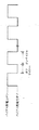
次いで,制御器112の制御により,プラズマ生成用電源120から整合器118を介して上部電極114に,27MHzで上部電極(114)1cm2当たり4W〜5Wの高周波電力を印加すると共に,バイアス用電源110から整合器108を介して下部電極106に,上記プラズマ生成用電力よりも相対的に低い周波数である800kHzでウェハW1cm2当たり5Wの高周波電力を後述の如く間欠的に印加する。
【0022】
ここで,図2〜図9を参照しながら,バイアス用電力の制御構成について説明する。
図3は,本実施の形態のバイアス用電力の供給構成,すなわち図4に示すバイアス用電力を印加するオンサイクル(以下,「エッチング工程」という。)から処理を開始して,9回のエッチング工程と,8回のバイアス用電力を印加しないオフサイクル(以下,「成膜工程」という。)とを交互に繰り返し,エッチング工程で処理を終了した時点でのウェハW上の一点における選択比(絶縁膜202のエッチングされた量/フォトレジスト膜206のエッチングされた量)と,デューティー(オンサイクル時間/(オンサイクル時間+オフサイクル時間))との関係を示している。また,上記オンサイクル時間は30秒に,オフサイクル時間はデューティーを満たす時間に設定されている。なお,デューティー100%とは,バイアス用電力を連続的に印加した場合である。また,成膜工程において,バイアス用電力を遮断するのと同程度の作用があるようにバイアス用電力を低減させても良い。
【0023】
図3より,デューティーを下げることにより選択比が向上することがわかる。この理由として以下のことが考えられる。下部電極106にバイアス用電力を印加している期間(エッチング工程)では,C4F8の解離によって生じるCFxイオンとCFxラジカル,およびArイオン等により絶縁膜202がイオンアシストエッチングされる。一方,フォトレジスト膜206は,絶縁膜202のエッチングレートよりも低いものの,上記イオンによりスパッタ(エッチング)される。
【0024】
また,バイアス用電力を印加していない期間(成膜工程)では,イオンがウェハWに引き寄せられない。その結果,図2(b)に示すように,CFxラジカルがフォトレジスト膜206の表面に付着することによってポリマー(重合体)208が形成される。同様に,絶縁膜202の表面にもポリマー208が形成される。しかし,絶縁膜202の表面は,少なくともフォトレジスト膜206の厚み分だけは深いところにあり,またラジカル粒子は熱運動(ランダム運動)をするので,絶縁膜202の表面に形成されるポリマー208の厚み(B)は,フォトレジスト膜206の表面に形成されるポリマー208の厚み(A)よりも薄い。この点については,図8を用いて後述する。
【0025】
さらに,フォトレジスト膜206は,例えばCxFyOzから成るため,SiO2から成る絶縁膜202よりもポリマー208に分子組成が近いためポリマー208が付着し易いと考えられる。この点については,図9を用いて後述する。
【0026】
また,成膜工程に続くエッチング工程では,ポリマー208がフォトレジスト膜206の保護膜として働く。つまり,まずポリマー208がエッチングされ,その後にフォトレジスト膜206がエッチングされるので,フォトレジスト膜206がエッチングされる量が減る。一方,絶縁膜202上のポリマー208は薄いので,絶縁膜202のエッチングの進行をさほど妨げることがない。
【0027】
また,エッチング工程では,絶縁膜202は約8000オングストローム/分,フォトレジスト膜206は約800オングストローム/分,保護膜であるポリマー208は約2300オングストローム/分でエッチングされる。これに対して,成膜工程では,ポリマー208は約1800オングストローム/分でフォトレジスト膜206の表面に成膜される。このことは,図3に示すように,バイアス用電力を常時印加した場合には選択比が10であり,そのバイアス用電力をデューティー50%で印加した場合には選択比が15になることに対応している。
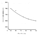
【0028】
また,図5は,図3と同じ条件でデューティーを変えたときの全処理時間と,絶縁膜202の平均エッチングレート(絶縁膜202のエッチング量/成膜工程を含む全処理時間)との関係を示している。図5より,デューティーを下げると,平均エッチングレートが低下し,全処理時間が長くなることがわかる。
【0029】
また,図6は,図3と同じ条件でデューティーを変えて全処理時間を終了した時点で残存しているフォトレジスト膜206の厚みを示している。図6より,デューティーを下げると,フォトレジスト膜206の残量が増加し,結果的に期待通りの形状のコンタクトホール210(図2(c)を参照。)が形成されることがわかる。
【0030】
また,図7(b)は,図7(a)に示す状態のウェハWに対して,所定時間の成膜工程を施した後におけるコンタクトホール210底面と,フォトレジスト膜206上面に形成されるポリマー208の状態を示したものである。また,図8は,図7(b)に示すコントクトホール210のアスペクト比を変えたときのフォトレジスト膜206上面に形成されるポリマー208の厚みAに対するコンタクトホール210底面に形成されるポリマー208の厚みBの比を示す。なお,本明細書中において,アスペクト比とは,図7(b)に示すフォトレジスト膜206の上面と絶縁膜202の底面との間の距離dと,コンタクトホール210の直径rの比(d/r)である。
【0031】
図8より,アスペクト比が大きくなるに従って,すなわちエッチングが進行してコンタクトホール210が深くなるに従って,コンタクトホール210底面に形成されるポリマー208の厚みBは,フォトレジスト膜206上面に形成されるポリマー208の厚みAに比べて薄くなることがわかる。
【0032】
また,図9は,図3と同じプロセス条件の成膜工程で,ウェハWの表面がフォトレジスト膜206の場合と,ウェハWの表面が絶縁膜(SiO2膜)202の場合のポリマー208の成膜速度を比較したものである。図9より,フォトレジスト膜206上に約120オングストロームのポリマー208が形成されるまでは,絶縁膜202上にはポリマー208が形成されない事がわかる。この程度の期間(5秒)では,バイアス用電力の印加を停止しても,絶縁膜202にはポリマー208等が形成されない。
【0033】
以上の実験データから以下のことが言える。図4では,上述の如くエッチング工程を1回当たり30秒とし,エッチング工程から始めてエッチング工程で終了する場合について示した。このように,最初の工程と最後の工程とがエッチング工程であれば,デューティーが同じであっても1回当たりのエッチング工程と成膜工程の時間を長くすることにより,全処理時間を短縮できる。
【0034】
また,本実施の形態では,エッチング工程を最終工程としているが,これは成膜工程を最終工程とすると,フォトレジスト膜206表面やコンタクトホール210底面にポリマー208等の反応生成物が付着したまま残るので,ポリマー等を除去する工程が余分に必要となり,スループットを低下させるからである。つまり,最終のエッチング工程では,ポリマー208を除去し,コンタクトホール210の形成が完了するまでエッチングが行われる。
【0035】
また,図9に示すように,成膜工程の時間が5秒であれば,絶縁膜202上にポリマー208が形成されず,フォトレジスト膜206上にポリマー208が形成される。上記時間は,使用する処理ガスの種類等のプロセス条件によって変わるが,少なくとも1秒以上であれば,フォトレジスト膜206上にポリマー208が形成されることもあり,上記と同様の効果を得ることができる。なお,処理時間を短くするためには,エッチング工程の時間を成膜工程の時間よりも一般的に長くすれば良い。また,本実施の形態では,バイアス用電力のオン・オフの周期が1秒以上であるので,特殊なパルス電源を用いなくてもソフトウェアによって電源のオン・オフを容易に制御できる。
【0036】
また,コンタクトホール210の径が小さい場合は,エッチングの開始時において所定のアスペクト比が確保されている。従って,図8に示すように,最初の工程を成膜工程としても,絶縁膜202には僅かなポリマー208が形成されるだけなので,エッチング速度をさほど低下させないと共に,予めフォトレジスト膜206にポリマー208を形成できるので,選択比を向上させることができる。
【0037】
また,コンタクトホール210は,エッチングが進行するに従ってアスペクト比が高くなり,成膜工程によりコンタクトホール210の底面に形成されるポリマー208の成膜速度は低下する。その結果,成膜工程によってコンタクトホール210のエッチングが妨げられる度合いは,エッチング開始時と比べて低下する。従って,エッチングに進行に合わせてデューティーを下げ,あるいはエッチング工程の時間を短くして成膜工程の時間を長くすれば,フォトレジスト膜206にポリマー208を確実に形成しながら,絶縁膜202に対しても所定のエッチングを施すことができる。
【0038】
また,本実施の形態を採用すれば,成膜工程においてフォトレジスト膜206上に形成されたポリマー208がエッチングされた後に,フォトレジスト膜206がエッチングされるので,選択比を高くすることができる。ただし,選択比を必要以上に高くすると,処理時間が長くなる。
【0039】
また,フォトレジスト膜206は,全処理を完了した時点で,図2(d)に示す悪い形状のコンタクトホール10が形成されない程度,エッチングされずに残っていれば充分である。従って,デューティーおよびエッチング・成膜工程1回当たりの夫々の時間は,絶縁膜202およびフォトレジスト膜206の厚み,絶縁膜202およびフォトレジスト膜206のエッチングレート,ポリマー208の成膜レート,コンタクトホールの径,エッチングの進行の度合い,処理ガスの種類,バイアス用電力の大きさ等を考慮して処理時間が最短になるように決められる。
【0040】
本実施の形態は,以上のように構成されており,フォトレジスト膜206の上面やその肩部にポリマー208を形成しながらエッチング処理を行うので,処理時にフォトレジスト膜206が過度にエッチングされて,特に図2(c)に示す肩部206aが損傷することがない。その結果,パターン204に基づいて,高アスペクト比のコンタクトホール210を確実に形成することができる。また,ポリマー208は,図2(b)に示すように,コンタクトホール210の内部側面にも付着するので,すでに形成されたコンタクトホール210の内部側壁がエッチングされ難くなり,いわゆるボーイング形状となることを防止できる。
【0041】
以上,本発明の好適な実施の一形態について,添付図面を参照しながら説明したが,本発明はかかる構成に限定されるものではない。特許請求の範囲に記載された技術的思想の範疇において,当業者であれば,各種の変更例および修正例に想到し得るものであり,それら変更例および修正例についても本発明の技術的範囲に属するものと了解される。
【0042】
例えば,上記実施の形態において,800kHzのバイアス用電力を下部電極に印加する構成を例に挙げて説明したが,800kHz以外の周波数の電力をバイアス用電力として採用しても,本発明を実施することができる。
【0043】
また,上記実施の形態において,絶縁膜としてSiO2を採用する構成を例に挙げて説明したが,本発明はかかる構成に限定されるものではなく,例えばBPSG(boron-phospho-silicate glass)や,TEOS(tetraethylorth-osilicate)や,SOG(spin on glass)や,SiOFや,熱酸化膜(SiO2)などの絶縁膜,あるいは絶縁膜以外のエッチング処理に対しても,本発明を適用することができる。
【0044】
さらに,上記実施の形態において,平行平板型プラズマエッチング装置を例に挙げて説明したが,本発明はかかる構成に限定されるものではなく,被処理体にバイアス用電力を印加できれば,誘導結合型エッチング装置やマイクロ波型エッチング装置などのプラズマ源を備えたプラズマエッチング装置にも,本発明を適用することができる。
【0045】
【発明の効果】
本発明によれば,エッチング処理中に,例えばフォトレジスト膜の露出面に保護膜を形成する成膜工程を設けたので,その保護膜によってフォトレジスト膜がエッチングされ難くなり,選択比を向上させることができる。その結果,処理終了時までフォトレジスト膜に形成されたエッチングパターンを初期の状態と実質的に同一の状態に維持することができ,上記パターンに基づいて,所定の超微細なコンタクトホールを形成することができる。さらに,コンタクトホールの内部側壁にも保護膜を形成し,保護することができるため,上記内部側壁面がエッチングされて生じるボーイング形状の発生を抑制することができ,所定形状のコンタクトホールを形成することができる。
【図面の簡単な説明】
【図1】本発明を適用可能なエッチング装置を示す概略的な断面図である。
【図2】図1に示すエッチング装置に適用されるエッチング方法と従来のエッチング方法を説明するためのウェハWを表す概略的な断面図である。
【図3】図1に示すエッチング装置に適用されるエッチング方法を説明するための選択比とデューティーとの関係を表す概略的な説明図である。
【図4】図1に示すエッチング装置に適用されるエッチング方法を説明するためのバイアス用電力のオン・オフサイクルを表す概略的な説明図である。
【図5】図1に示すエッチング装置に適用されるエッチング方法を説明するためのデューティーを変化させた際の全処理時間と絶縁膜のエッチングレートとの関係を表す概略的な説明図である。
【図6】図1に示すエッチング装置に適用されるエッチング方法を説明するためのフォトレジスト膜の残膜厚みとデューティーとの関係を表す概略的な説明図である。
【図7】図1に示すエッチング装置に適用されるエッチング方法を説明するためのウェハWを表す概略的な断面図である。
【図8】図1に示すエッチング装置に適用されるエッチング方法を説明するためのアスペクト比とポリマーの厚みとの関係を表す概略的な説明図である。
【図9】図1に示すエッチング装置に適用されるエッチング方法を説明するためのバイアス用電力オフ時間とポリマーの厚みとの関係を表す概略的な断面図である。
【符号の説明】
100 エッチング装置
102 処理室
106 下部電極
110 バイアス用電源
112 制御器
114 上部電極
120 プラズマ生成用電源
200 基板
202 絶縁膜
206 フォトレジスト膜
208 ポリマー(保護膜)
210 コンタクトホール
W ウェハ[0001]
BACKGROUND OF THE INVENTION
The present invention relates to a plasma etching method and a plasma etching apparatus.
[0002]
[Prior art]
Conventionally, a plasma etching apparatus has been proposed in which an upper electrode and a lower electrode are opposed to each other in an airtight processing chamber. In this apparatus, first, a target object, for example, a semiconductor wafer (hereinafter referred to as “wafer”) is placed on the lower electrode, and then a processing gas is introduced into the processing chamber and the processing chamber is evacuated to a predetermined level. Maintain the pressure atmosphere. Next, the plasma generation power is applied to the upper electrode, and the bias power maintained at a constant power is applied to the lower electrode. As a result, the processing gas in the processing chamber is dissociated to generate plasma and radicals, and SiO 2 (silicon oxide) formed on the wafer by the radicals and ions in the plasma drawn into the wafer by the bias power. An insulating film such as a film is ion-assisted etched to form a contact hole in the insulating film.
[0003]
[Problems to be solved by the invention]
However, when the contact hole is formed under the 0.15 μm design rule, the aspect ratio increases and the etching rate of the insulating film decreases. The photoresist film formed on the surface of the insulating film is always sputtered by ions. At this time, many corners formed between the upper surface of the photoresist film and the pattern formation surface are sputtered. As a result, as shown in FIG. 2D, the pattern width of the
[0004]
The present invention has been made in view of the above-mentioned problems of the prior art, and a first object of the present invention is to improve the etching selectivity and to perform ultra-fine etching on a workpiece. It is to provide a new and improved plasma etching method that can be processed.
[0005]
A second object of the present invention is to provide a new and improved plasma etching apparatus capable of forming a contact hole having a predetermined shape in a workpiece.
[0006]
[Means for Solving the Problems]
In order to solve the above problems, according to a first aspect of the present invention, as in the first aspect of the present invention, a processing gas is introduced into a processing chamber and plasma is generated in the processing chamber by a plasma source. A plasma etching method in which bias power is applied to an electrode disposed in a processing chamber, and a predetermined etching process is performed on an object to be processed placed on the electrode, and the bias power is applied to the electrode. Then, an etching process for etching the object to be processed for a predetermined etching time, and a film formation for forming a protective film on the etching mask on the surface of the object to be processed for a predetermined film forming time by reducing or cutting off the bias power. sequentially repeating the deposition step, at that time, each of the etching time and the and the film depositing time, characterized in that it is changed in accordance with progress of the etching process, Purazumae Quenching method is provided.
[0007]
According to such a configuration, the etching process is performed while repeating the etching process and the film forming process, so that the object to be processed can be etched while protecting the etching mask, for example, the photoresist film, with the protective film. As a result, the photoresist film becomes difficult to be etched and the selection ratio increases, so that the expansion of the pattern of the photoresist film can be suppressed, and a protective film is also formed on the mask pattern side wall during the film forming process. , A desired contact hole can be formed in the object to be processed. In addition, if each etching time and each film formation time are changed according to the progress of the etching process, a predetermined etching process can be performed even if the state of the object to be processed and the photoresist film changes due to the progress of the process. Can do.
[0009]
Further, each film formation time may be relatively extended according to the progress of the etching process, for example, as in the invention described in
[0010]
Furthermore, if each film formation time is set to 1 second or longer, for example, as in the invention described in
[0011]
Further, as the final step of the etching process, for example, if the etching step is performed as in the invention described in
[0012]
Furthermore, as a starting process of the etching process, for example, if a film forming process is performed as in the invention described in
[0013]
Furthermore, for example, when a silicon oxide film is used as an etching object and a gas containing a fluorocarbon gas is used as a processing gas as in the invention described in
[0014]
According to the second aspect of the present invention, as in the invention according to
[0015]
According to such a configuration, since the bias power is intermittently applied to the electrodes, as in the first aspect of the present invention, when the bias power is applied, the object to be processed is etched and the bias power is applied. When reducing or blocking, a protective film can be formed on the etching mask of the object to be processed, and a desired contact hole can be formed in the object to be processed. In addition, if each etching time and each film formation time are changed according to the progress of the etching process, a predetermined etching process can be performed even if the state of the object to be processed and the photoresist film changes due to the progress of the process. Can do.
[0016]
DETAILED DESCRIPTION OF THE INVENTION
Hereinafter, an embodiment of a plasma etching method and a plasma etching apparatus according to the present invention will be described with reference to the accompanying drawings.
[0017]
(1) Overall Configuration of Etching Apparatus First, the overall configuration of a parallel plate
The
[0018]
A conductive upper electrode 114 is disposed at a position facing the mounting surface of the
[0019]
Further, the upper electrode 114 is formed with a number of gas discharge holes 114 a, and a processing gas supply source (not shown) is connected to the gas discharge holes 114 a through a
[0020]
(2) Etching Process Next, the etching process of the present embodiment will be described in detail with reference to FIGS.
First, the wafer W is mounted on the
[0021]
Next, under the control of the
[0022]
Here, the control configuration of the bias power will be described with reference to FIGS.
FIG. 3 shows the bias power supply configuration of this embodiment, that is, the etching starts nine times from the on cycle (hereinafter referred to as “etching process”) in which the bias power shown in FIG. 4 is applied. The selection ratio at one point on the wafer W at the time when the process and the off cycle (hereinafter referred to as “film formation process”) where no bias power is applied are repeated alternately and the process is completed in the etching process ( The relationship between the etched amount of the insulating
[0023]
FIG. 3 shows that the selection ratio is improved by lowering the duty. The following can be considered as this reason. In a period (etching process) in which bias power is applied to the
[0024]
Further, ions are not attracted to the wafer W during a period in which the bias power is not applied (film formation process). As a result, as shown in FIG. 2B, CF x radicals adhere to the surface of the
[0025]
Furthermore, since the
[0026]
In the etching process subsequent to the film forming process, the
[0027]
In the etching process, the insulating
[0028]
FIG. 5 shows the relationship between the total processing time when the duty is changed under the same conditions as in FIG. 3 and the average etching rate of the insulating film 202 (the etching amount of the insulating
[0029]
FIG. 6 shows the thickness of the
[0030]
7B is formed on the bottom surface of the
[0031]
From FIG. 8, the thickness B of the
[0032]
FIG. 9 is a film forming process under the same process conditions as in FIG. 3. In the case where the surface of the wafer W is a
[0033]
The following can be said from the above experimental data. FIG. 4 shows a case where the etching process is set to 30 seconds per time as described above, and the etching process starts and ends. In this way, if the first process and the last process are etching processes, the total processing time can be shortened by increasing the time of the etching process and the film forming process per time even if the duty is the same. .
[0034]
In this embodiment, the etching process is the final process. When the film forming process is the final process, the reaction product such as the
[0035]
As shown in FIG. 9, if the film forming process time is 5 seconds, the
[0036]
When the diameter of the
[0037]
In addition, the aspect ratio of the
[0038]
Further, if this embodiment is adopted, the
[0039]
Further, it is sufficient that the
[0040]
The present embodiment is configured as described above, and the etching process is performed while forming the
[0041]
The preferred embodiment of the present invention has been described above with reference to the accompanying drawings, but the present invention is not limited to such a configuration. Within the scope of the technical idea described in the claims, those skilled in the art will be able to conceive of various changes and modifications, and these changes and modifications are also within the technical scope of the present invention. It is understood that it belongs to.
[0042]
For example, in the above-described embodiment, the configuration in which 800 kHz bias power is applied to the lower electrode has been described as an example. However, the present invention can be implemented even when power having a frequency other than 800 kHz is used as the bias power. be able to.
[0043]
Further, in the above-described embodiment, the configuration employing SiO 2 as the insulating film has been described as an example. However, the present invention is not limited to such a configuration, and for example, BPSG (boron-phospho-silicate glass), , TEOS (tetraethylorth-osilicate), SOG (spin on glass), SiOF, insulating film such as thermal oxide film (SiO 2 ), etc., or the etching process other than the insulating film should be applied. Can do.
[0044]
Furthermore, in the above embodiment, the parallel plate type plasma etching apparatus has been described as an example. However, the present invention is not limited to such a configuration, and an inductive coupling type can be used as long as a bias power can be applied to the object to be processed. The present invention can also be applied to a plasma etching apparatus having a plasma source such as an etching apparatus or a microwave etching apparatus.
[0045]
【The invention's effect】
According to the present invention, during the etching process, for example, a film forming step for forming a protective film on the exposed surface of the photoresist film is provided. Therefore, the photoresist film is hardly etched by the protective film, and the selectivity is improved. be able to. As a result, the etching pattern formed on the photoresist film can be maintained in substantially the same state as the initial state until the end of processing, and a predetermined ultrafine contact hole is formed based on the pattern. be able to. Further, since a protective film can be formed and protected on the inner side wall of the contact hole, it is possible to suppress the occurrence of a bowing shape caused by etching the inner side wall surface, and to form a contact hole having a predetermined shape. be able to.
[Brief description of the drawings]
FIG. 1 is a schematic cross-sectional view showing an etching apparatus to which the present invention can be applied.
FIG. 2 is a schematic cross-sectional view showing a wafer W for explaining an etching method applied to the etching apparatus shown in FIG. 1 and a conventional etching method.
3 is a schematic explanatory diagram showing a relationship between a selection ratio and a duty for explaining an etching method applied to the etching apparatus shown in FIG. 1; FIG.
4 is a schematic explanatory view showing an on / off cycle of bias power for explaining an etching method applied to the etching apparatus shown in FIG. 1; FIG.
FIG. 5 is a schematic explanatory diagram showing the relationship between the total processing time and the etching rate of the insulating film when changing the duty for explaining the etching method applied to the etching apparatus shown in FIG. 1;
6 is a schematic explanatory view showing the relationship between the residual film thickness of the photoresist film and the duty for explaining the etching method applied to the etching apparatus shown in FIG. 1; FIG.
7 is a schematic cross-sectional view showing a wafer W for explaining an etching method applied to the etching apparatus shown in FIG. 1;
8 is a schematic explanatory diagram showing the relationship between the aspect ratio and the thickness of a polymer for explaining an etching method applied to the etching apparatus shown in FIG. 1;
9 is a schematic cross-sectional view showing a relationship between a bias power off time and a polymer thickness for explaining an etching method applied to the etching apparatus shown in FIG. 1; FIG.
[Explanation of symbols]
DESCRIPTION OF
210 Contact hole W Wafer
Claims (6)
前記バイアス用電力を前記電極に印加して所定のエッチング時間にわたり前記被処理体にエッチングを施すエッチング工程と,前記バイアス用電力を低減または遮断して所定の成膜時間にわたり前記被処理体表面のエッチングマスクに保護膜を形成する成膜を施す成膜工程とを順次反復し,
前記エッチング処理が進行するに従いデューティー比を小さくするように前記バイアス用電力の印加、低減または遮断を制御することを特徴とする,プラズマエッチング方法。An object to be processed placed on the electrode by introducing a processing gas into the processing chamber, generating plasma in the processing chamber by a plasma source, and applying a bias power to an electrode disposed in the processing chamber A plasma etching method for performing a predetermined etching process on
An etching step in which the bias power is applied to the electrode to etch the object to be processed for a predetermined etching time; and the bias power is reduced or cut off to form a surface of the object to be processed for a predetermined film formation time. Sequentially repeating the film forming process for forming a protective film on the etching mask ,
A plasma etching method , wherein application, reduction or interruption of the bias power is controlled so as to reduce a duty ratio as the etching process proceeds .
前記処理ガスは,フルオロカーボンガスを含むガスであることを特徴とする,請求項1〜4のいずれかに記載のプラズマエッチング方法。The etching object is a silicon oxide film,
The process gas, characterized in that it is a gas containing fluorocarbon gas plasma etching method according to any one of claims 1-4.
前記電極には,所定のエッチング時間にわたり前記バイアス用電力を出力し,所定の成膜時間にわたり前記バイアス用電力を低減または遮断すると共に,前記バイアス用電力の出力と低減または遮断とを1秒以上の周期で順次反復するバイアス用電源が接続され,
前記バイアス用電源から出力される前記バイアス用電力の印加、低減または遮断は、前記エッチング処理が進行するに従いデューティー比を小さくするように制御されることを特徴とする,プラズマエッチング装置。An object to be processed placed on the electrode by introducing a processing gas into the processing chamber, generating plasma in the processing chamber by a plasma source, and applying a bias power to an electrode disposed in the processing chamber A plasma etching apparatus for performing a predetermined etching process on
The electrode outputs the bias power over a predetermined etching time, reduces or cuts off the bias power over a predetermined film formation time, and outputs and reduces or cuts off the bias power for one second or longer. bias power source for sequentially repeating a cycle of being connected,
The plasma etching apparatus according to claim 1, wherein application, reduction or interruption of the bias power output from the bias power source is controlled so as to reduce a duty ratio as the etching process proceeds .
Priority Applications (6)
| Application Number | Priority Date | Filing Date | Title |
|---|---|---|---|
| JP31994298A JP4153606B2 (en) | 1998-10-22 | 1998-10-22 | Plasma etching method and plasma etching apparatus |
| DE69942372T DE69942372D1 (en) | 1998-10-22 | 1999-10-22 | plasma etching |
| PCT/JP1999/005821 WO2000024046A1 (en) | 1998-10-22 | 1999-10-22 | Plasma etching method |
| KR1020017004885A KR100590370B1 (en) | 1998-10-22 | 1999-10-22 | Plasma etching method |
| EP99949351A EP1143496B1 (en) | 1998-10-22 | 1999-10-22 | Plasma etching method |
| US09/807,896 US6793832B1 (en) | 1998-10-22 | 1999-10-22 | Plasma etching method |
Applications Claiming Priority (1)
| Application Number | Priority Date | Filing Date | Title |
|---|---|---|---|
| JP31994298A JP4153606B2 (en) | 1998-10-22 | 1998-10-22 | Plasma etching method and plasma etching apparatus |
Publications (3)
| Publication Number | Publication Date |
|---|---|
| JP2000133638A JP2000133638A (en) | 2000-05-12 |
| JP2000133638A5 JP2000133638A5 (en) | 2005-11-04 |
| JP4153606B2 true JP4153606B2 (en) | 2008-09-24 |
Family
ID=18115972
Family Applications (1)
| Application Number | Title | Priority Date | Filing Date |
|---|---|---|---|
| JP31994298A Expired - Lifetime JP4153606B2 (en) | 1998-10-22 | 1998-10-22 | Plasma etching method and plasma etching apparatus |
Country Status (6)
| Country | Link |
|---|---|
| US (1) | US6793832B1 (en) |
| EP (1) | EP1143496B1 (en) |
| JP (1) | JP4153606B2 (en) |
| KR (1) | KR100590370B1 (en) |
| DE (1) | DE69942372D1 (en) |
| WO (1) | WO2000024046A1 (en) |
Families Citing this family (31)
| Publication number | Priority date | Publication date | Assignee | Title |
|---|---|---|---|---|
| KR100327346B1 (en) * | 1999-07-20 | 2002-03-06 | 윤종용 | Plasma etching method using selective polymer deposition and method for forming contact hole using the plasma etching method |
| KR20020017182A (en) * | 2000-08-29 | 2002-03-07 | 윤종용 | Method for manufacturing semiconductor device using octafluorobutene etching gas |
| DE10053780A1 (en) * | 2000-10-30 | 2002-05-16 | Infineon Technologies Ag | Process for structuring a silicon oxide layer |
| US7169695B2 (en) * | 2002-10-11 | 2007-01-30 | Lam Research Corporation | Method for forming a dual damascene structure |
| KR100517075B1 (en) | 2003-08-11 | 2005-09-26 | 삼성전자주식회사 | Method for manufacturing semiconductor device |
| KR100656708B1 (en) | 2005-04-01 | 2006-12-13 | 주식회사 에이디피엔지니어링 | Plasma processing apparatus |
| JP4653603B2 (en) * | 2005-09-13 | 2011-03-16 | 株式会社日立ハイテクノロジーズ | Plasma etching method |
| US7488687B2 (en) | 2006-09-12 | 2009-02-10 | Samsung Electronics Co., Ltd. | Methods of forming electrical interconnect structures using polymer residues to increase etching selectivity through dielectric layers |
| US7491343B2 (en) | 2006-09-14 | 2009-02-17 | Lam Research Corporation | Line end shortening reduction during etch |
| US7407597B2 (en) * | 2006-09-14 | 2008-08-05 | Lam Research Corporation | Line end shortening reduction during etch |
| US7547636B2 (en) * | 2007-02-05 | 2009-06-16 | Lam Research Corporation | Pulsed ultra-high aspect ratio dielectric etch |
| US7737042B2 (en) * | 2007-02-22 | 2010-06-15 | Applied Materials, Inc. | Pulsed-plasma system for etching semiconductor structures |
| US7771606B2 (en) * | 2007-02-22 | 2010-08-10 | Applied Materials, Inc. | Pulsed-plasma system with pulsed reaction gas replenish for etching semiconductors structures |
| US7718538B2 (en) * | 2007-02-21 | 2010-05-18 | Applied Materials, Inc. | Pulsed-plasma system with pulsed sample bias for etching semiconductor substrates |
| CN101636813B (en) * | 2007-03-12 | 2013-02-27 | 艾克斯特朗股份公司 | Novel plasma system for improved process capability |
| US7846846B2 (en) * | 2007-09-25 | 2010-12-07 | Applied Materials, Inc. | Method of preventing etch profile bending and bowing in high aspect ratio openings by treating a polymer formed on the opening sidewalls |
| JP5268625B2 (en) * | 2008-12-26 | 2013-08-21 | 株式会社日立ハイテクノロジーズ | Plasma processing equipment |
| KR101037043B1 (en) * | 2009-02-27 | 2011-05-26 | 성균관대학교산학협력단 | Method for forming via in a semiconductor substrate |
| US9478408B2 (en) | 2014-06-06 | 2016-10-25 | Lam Research Corporation | Systems and methods for removing particles from a substrate processing chamber using RF plasma cycling and purging |
| US10081869B2 (en) | 2014-06-10 | 2018-09-25 | Lam Research Corporation | Defect control in RF plasma substrate processing systems using DC bias voltage during movement of substrates |
| US10047438B2 (en) | 2014-06-10 | 2018-08-14 | Lam Research Corporation | Defect control and stability of DC bias in RF plasma-based substrate processing systems using molecular reactive purge gas |
| CN105719965A (en) * | 2014-12-04 | 2016-06-29 | 北京北方微电子基地设备工艺研究中心有限责任公司 | Method and device for etching silicon dioxide substrate |
| JP6504827B2 (en) * | 2015-01-16 | 2019-04-24 | 東京エレクトロン株式会社 | Etching method |
| US9691625B2 (en) * | 2015-11-04 | 2017-06-27 | Lam Research Corporation | Methods and systems for plasma etching using bi-modal process gas composition responsive to plasma power level |
| JP6833657B2 (en) | 2017-11-07 | 2021-02-24 | 東京エレクトロン株式会社 | How to plasma etch the substrate |
| JP2019212776A (en) * | 2018-06-05 | 2019-12-12 | 東京エレクトロン株式会社 | Composition for deposition and deposition apparatus |
| JP2019212777A (en) * | 2018-06-05 | 2019-12-12 | 東京エレクトロン株式会社 | Composition for deposition and deposition apparatus |
| US10593518B1 (en) * | 2019-02-08 | 2020-03-17 | Applied Materials, Inc. | Methods and apparatus for etching semiconductor structures |
| US11456180B2 (en) | 2019-11-08 | 2022-09-27 | Tokyo Electron Limited | Etching method |
| WO2021090516A1 (en) * | 2019-11-08 | 2021-05-14 | 東京エレクトロン株式会社 | Etching method |
| WO2024204321A1 (en) * | 2023-03-28 | 2024-10-03 | 東京エレクトロン株式会社 | Etching device and etching method |
Family Cites Families (8)
| Publication number | Priority date | Publication date | Assignee | Title |
|---|---|---|---|---|
| US4855017A (en) * | 1985-05-03 | 1989-08-08 | Texas Instruments Incorporated | Trench etch process for a single-wafer RIE dry etch reactor |
| KR900007687B1 (en) * | 1986-10-17 | 1990-10-18 | 가부시기가이샤 히다찌세이사꾸쇼 | Method and device for plasma processing |
| JP2918892B2 (en) * | 1988-10-14 | 1999-07-12 | 株式会社日立製作所 | Plasma etching method |
| US5888414A (en) | 1991-06-27 | 1999-03-30 | Applied Materials, Inc. | Plasma reactor and processes using RF inductive coupling and scavenger temperature control |
| EP0552491B1 (en) * | 1992-01-24 | 1998-07-15 | Applied Materials, Inc. | Plasma etch process and plasma processing reactor |
| JP2625072B2 (en) * | 1992-09-08 | 1997-06-25 | アプライド マテリアルズ インコーポレイテッド | Plasma reactor using electromagnetic RF coupling and method thereof |
| US5573597A (en) * | 1995-06-07 | 1996-11-12 | Sony Corporation | Plasma processing system with reduced particle contamination |
| EP0822582B1 (en) | 1996-08-01 | 2003-10-01 | Surface Technology Systems Plc | Method of etching substrates |
-
1998
- 1998-10-22 JP JP31994298A patent/JP4153606B2/en not_active Expired - Lifetime
-
1999
- 1999-10-22 WO PCT/JP1999/005821 patent/WO2000024046A1/en active IP Right Grant
- 1999-10-22 EP EP99949351A patent/EP1143496B1/en not_active Expired - Lifetime
- 1999-10-22 KR KR1020017004885A patent/KR100590370B1/en active IP Right Grant
- 1999-10-22 DE DE69942372T patent/DE69942372D1/en not_active Expired - Lifetime
- 1999-10-22 US US09/807,896 patent/US6793832B1/en not_active Expired - Lifetime
Also Published As
| Publication number | Publication date |
|---|---|
| EP1143496A1 (en) | 2001-10-10 |
| EP1143496A4 (en) | 2006-12-13 |
| WO2000024046A1 (en) | 2000-04-27 |
| KR100590370B1 (en) | 2006-06-15 |
| KR20010080234A (en) | 2001-08-22 |
| US6793832B1 (en) | 2004-09-21 |
| JP2000133638A (en) | 2000-05-12 |
| EP1143496B1 (en) | 2010-05-12 |
| DE69942372D1 (en) | 2010-06-24 |
Similar Documents
| Publication | Publication Date | Title |
|---|---|---|
| JP4153606B2 (en) | Plasma etching method and plasma etching apparatus | |
| US10629473B2 (en) | Footing removal for nitride spacer | |
| EP1053563B1 (en) | Methods for reducing mask erosion during plasma etching | |
| US5660682A (en) | Plasma clean with hydrogen gas | |
| JP4852196B2 (en) | Method for etching a silicon layer in a plasma processing chamber to form a deep opening | |
| JP2915807B2 (en) | Etching of molybdenum silicide using sulfur hexafluoride, hydrogen bromide and oxygen | |
| JP5214596B2 (en) | Method for minimizing mask undercuts and notches in plasma processing systems | |
| JPH06275568A (en) | Dry etching method | |
| JP4209774B2 (en) | Silicon substrate etching method and etching apparatus | |
| JP3213803B2 (en) | Method for forming slope contact hole in semiconductor using high-density plasma etching equipment | |
| JP2010500758A (en) | Mask layer processing method before performing etching process | |
| JPH06177092A (en) | Manufacture of semiconductor device | |
| TWI389865B (en) | Notch stop pulsing process for plasma processing system | |
| JP4184851B2 (en) | Plasma processing method | |
| WO2003056617A1 (en) | Etching method and plasma etching device | |
| US6756314B2 (en) | Method for etching a hard mask layer and a metal layer | |
| JP3970600B2 (en) | Etching method | |
| JP2022067033A (en) | Substrate processing method and substrate processing apparatus | |
| JP2894304B2 (en) | Method for manufacturing semiconductor device | |
| KR100851455B1 (en) | New methodologies to reduce process sensitivity to the chamber condition | |
| JP7498367B2 (en) | Plasma treatment method | |
| JP2003068709A (en) | Dry etching method | |
| KR20220082979A (en) | Substrate processing method of substrate processing apparatus | |
| JP3256082B2 (en) | Plasma cleaning method | |
| JPH0794482A (en) | Dry etching method |
Legal Events
| Date | Code | Title | Description |
|---|---|---|---|
| A521 | Written amendment |
Free format text: JAPANESE INTERMEDIATE CODE: A523 Effective date: 20050920 |
|
| A621 | Written request for application examination |
Free format text: JAPANESE INTERMEDIATE CODE: A621 Effective date: 20050920 |
|
| A131 | Notification of reasons for refusal |
Free format text: JAPANESE INTERMEDIATE CODE: A131 Effective date: 20080408 |
|
| A521 | Written amendment |
Free format text: JAPANESE INTERMEDIATE CODE: A523 Effective date: 20080603 |
|
| TRDD | Decision of grant or rejection written | ||
| A01 | Written decision to grant a patent or to grant a registration (utility model) |
Free format text: JAPANESE INTERMEDIATE CODE: A01 Effective date: 20080701 |
|
| A01 | Written decision to grant a patent or to grant a registration (utility model) |
Free format text: JAPANESE INTERMEDIATE CODE: A01 |
|
| A61 | First payment of annual fees (during grant procedure) |
Free format text: JAPANESE INTERMEDIATE CODE: A61 Effective date: 20080704 |
|
| R150 | Certificate of patent or registration of utility model |
Free format text: JAPANESE INTERMEDIATE CODE: R150 |
|
| FPAY | Renewal fee payment (event date is renewal date of database) |
Free format text: PAYMENT UNTIL: 20110711 Year of fee payment: 3 |
|
| FPAY | Renewal fee payment (event date is renewal date of database) |
Free format text: PAYMENT UNTIL: 20110711 Year of fee payment: 3 |
|
| FPAY | Renewal fee payment (event date is renewal date of database) |
Free format text: PAYMENT UNTIL: 20140711 Year of fee payment: 6 |
|
| R250 | Receipt of annual fees |
Free format text: JAPANESE INTERMEDIATE CODE: R250 |
|
| R250 | Receipt of annual fees |
Free format text: JAPANESE INTERMEDIATE CODE: R250 |
|
| EXPY | Cancellation because of completion of term |