JP2020004705A - ディスプレイ装置 - Google Patents
ディスプレイ装置 Download PDFInfo
- Publication number
- JP2020004705A JP2020004705A JP2019068430A JP2019068430A JP2020004705A JP 2020004705 A JP2020004705 A JP 2020004705A JP 2019068430 A JP2019068430 A JP 2019068430A JP 2019068430 A JP2019068430 A JP 2019068430A JP 2020004705 A JP2020004705 A JP 2020004705A
- Authority
- JP
- Japan
- Prior art keywords
- layer
- groove
- substrate
- inorganic
- sealing layer
- Prior art date
- Legal status (The legal status is an assumption and is not a legal conclusion. Google has not performed a legal analysis and makes no representation as to the accuracy of the status listed.)
- Granted
Links
- 239000000758 substrate Substances 0.000 claims abstract description 104
- 230000000149 penetrating effect Effects 0.000 claims abstract description 16
- 238000007789 sealing Methods 0.000 claims description 131
- 239000010409 thin film Substances 0.000 claims description 25
- 238000000034 method Methods 0.000 claims description 13
- 239000010410 layer Substances 0.000 description 284
- 239000010408 film Substances 0.000 description 37
- 239000000463 material Substances 0.000 description 21
- 230000002093 peripheral effect Effects 0.000 description 19
- PXHVJJICTQNCMI-UHFFFAOYSA-N Nickel Chemical compound [Ni] PXHVJJICTQNCMI-UHFFFAOYSA-N 0.000 description 12
- 239000000126 substance Substances 0.000 description 11
- QVGXLLKOCUKJST-UHFFFAOYSA-N atomic oxygen Chemical compound [O] QVGXLLKOCUKJST-UHFFFAOYSA-N 0.000 description 10
- 229910052760 oxygen Inorganic materials 0.000 description 10
- 239000001301 oxygen Substances 0.000 description 10
- BASFCYQUMIYNBI-UHFFFAOYSA-N platinum Chemical compound [Pt] BASFCYQUMIYNBI-UHFFFAOYSA-N 0.000 description 10
- 239000010936 titanium Substances 0.000 description 9
- 229920000642 polymer Polymers 0.000 description 8
- 229910052709 silver Inorganic materials 0.000 description 8
- KDLHZDBZIXYQEI-UHFFFAOYSA-N Palladium Chemical compound [Pd] KDLHZDBZIXYQEI-UHFFFAOYSA-N 0.000 description 7
- 229910052751 metal Inorganic materials 0.000 description 7
- 239000002184 metal Substances 0.000 description 7
- 229910052581 Si3N4 Inorganic materials 0.000 description 6
- VYPSYNLAJGMNEJ-UHFFFAOYSA-N Silicium dioxide Chemical compound O=[Si]=O VYPSYNLAJGMNEJ-UHFFFAOYSA-N 0.000 description 6
- BQCADISMDOOEFD-UHFFFAOYSA-N Silver Chemical compound [Ag] BQCADISMDOOEFD-UHFFFAOYSA-N 0.000 description 6
- XLOMVQKBTHCTTD-UHFFFAOYSA-N Zinc monoxide Chemical compound [Zn]=O XLOMVQKBTHCTTD-UHFFFAOYSA-N 0.000 description 6
- 229910052782 aluminium Inorganic materials 0.000 description 6
- 239000011575 calcium Substances 0.000 description 6
- 239000011651 chromium Substances 0.000 description 6
- 239000010949 copper Substances 0.000 description 6
- 239000011229 interlayer Substances 0.000 description 6
- 239000011777 magnesium Substances 0.000 description 6
- 239000011368 organic material Substances 0.000 description 6
- 230000036961 partial effect Effects 0.000 description 6
- 230000035515 penetration Effects 0.000 description 6
- 230000001681 protective effect Effects 0.000 description 6
- HQVNEWCFYHHQES-UHFFFAOYSA-N silicon nitride Chemical compound N12[Si]34N5[Si]62N3[Si]51N64 HQVNEWCFYHHQES-UHFFFAOYSA-N 0.000 description 6
- 229910052814 silicon oxide Inorganic materials 0.000 description 6
- 239000004332 silver Substances 0.000 description 6
- 239000004642 Polyimide Substances 0.000 description 5
- RTAQQCXQSZGOHL-UHFFFAOYSA-N Titanium Chemical compound [Ti] RTAQQCXQSZGOHL-UHFFFAOYSA-N 0.000 description 5
- 229910045601 alloy Inorganic materials 0.000 description 5
- 239000000956 alloy Substances 0.000 description 5
- 238000005229 chemical vapour deposition Methods 0.000 description 5
- 238000005538 encapsulation Methods 0.000 description 5
- 239000010931 gold Substances 0.000 description 5
- 229910052759 nickel Inorganic materials 0.000 description 5
- 239000012044 organic layer Substances 0.000 description 5
- -1 polyethylene terephthalate Polymers 0.000 description 5
- 229920001721 polyimide Polymers 0.000 description 5
- 239000002356 single layer Substances 0.000 description 5
- 229910052719 titanium Inorganic materials 0.000 description 5
- GYHNNYVSQQEPJS-UHFFFAOYSA-N Gallium Chemical compound [Ga] GYHNNYVSQQEPJS-UHFFFAOYSA-N 0.000 description 4
- ZOKXTWBITQBERF-UHFFFAOYSA-N Molybdenum Chemical compound [Mo] ZOKXTWBITQBERF-UHFFFAOYSA-N 0.000 description 4
- XUIMIQQOPSSXEZ-UHFFFAOYSA-N Silicon Chemical compound [Si] XUIMIQQOPSSXEZ-UHFFFAOYSA-N 0.000 description 4
- 229910052804 chromium Inorganic materials 0.000 description 4
- 229910052733 gallium Inorganic materials 0.000 description 4
- 229910052749 magnesium Inorganic materials 0.000 description 4
- 229910052750 molybdenum Inorganic materials 0.000 description 4
- 239000011733 molybdenum Substances 0.000 description 4
- 238000005192 partition Methods 0.000 description 4
- 229910052697 platinum Inorganic materials 0.000 description 4
- 230000002829 reductive effect Effects 0.000 description 4
- 229910052710 silicon Inorganic materials 0.000 description 4
- 239000010703 silicon Substances 0.000 description 4
- VYZAMTAEIAYCRO-UHFFFAOYSA-N Chromium Chemical compound [Cr] VYZAMTAEIAYCRO-UHFFFAOYSA-N 0.000 description 3
- RYGMFSIKBFXOCR-UHFFFAOYSA-N Copper Chemical compound [Cu] RYGMFSIKBFXOCR-UHFFFAOYSA-N 0.000 description 3
- 229910052779 Neodymium Inorganic materials 0.000 description 3
- XAGFODPZIPBFFR-UHFFFAOYSA-N aluminium Chemical compound [Al] XAGFODPZIPBFFR-UHFFFAOYSA-N 0.000 description 3
- 229910052791 calcium Inorganic materials 0.000 description 3
- 229910052802 copper Inorganic materials 0.000 description 3
- 229910052737 gold Inorganic materials 0.000 description 3
- 239000012535 impurity Substances 0.000 description 3
- 238000007373 indentation Methods 0.000 description 3
- 238000002347 injection Methods 0.000 description 3
- 239000007924 injection Substances 0.000 description 3
- 229910052741 iridium Inorganic materials 0.000 description 3
- 229910052744 lithium Inorganic materials 0.000 description 3
- PQXKHYXIUOZZFA-UHFFFAOYSA-M lithium fluoride Inorganic materials [Li+].[F-] PQXKHYXIUOZZFA-UHFFFAOYSA-M 0.000 description 3
- 230000004048 modification Effects 0.000 description 3
- 238000012986 modification Methods 0.000 description 3
- 229910052763 palladium Inorganic materials 0.000 description 3
- 229920000058 polyacrylate Polymers 0.000 description 3
- 239000005020 polyethylene terephthalate Substances 0.000 description 3
- 229920000139 polyethylene terephthalate Polymers 0.000 description 3
- 230000008569 process Effects 0.000 description 3
- 239000011241 protective layer Substances 0.000 description 3
- 239000004065 semiconductor Substances 0.000 description 3
- WFKWXMTUELFFGS-UHFFFAOYSA-N tungsten Chemical compound [W] WFKWXMTUELFFGS-UHFFFAOYSA-N 0.000 description 3
- 229910052721 tungsten Inorganic materials 0.000 description 3
- 239000010937 tungsten Substances 0.000 description 3
- 239000011787 zinc oxide Substances 0.000 description 3
- OYPRJOBELJOOCE-UHFFFAOYSA-N Calcium Chemical compound [Ca] OYPRJOBELJOOCE-UHFFFAOYSA-N 0.000 description 2
- 229920008347 Cellulose acetate propionate Polymers 0.000 description 2
- 229910001374 Invar Inorganic materials 0.000 description 2
- XEEYBQQBJWHFJM-UHFFFAOYSA-N Iron Chemical compound [Fe] XEEYBQQBJWHFJM-UHFFFAOYSA-N 0.000 description 2
- WHXSMMKQMYFTQS-UHFFFAOYSA-N Lithium Chemical compound [Li] WHXSMMKQMYFTQS-UHFFFAOYSA-N 0.000 description 2
- FYYHWMGAXLPEAU-UHFFFAOYSA-N Magnesium Chemical compound [Mg] FYYHWMGAXLPEAU-UHFFFAOYSA-N 0.000 description 2
- URLKBWYHVLBVBO-UHFFFAOYSA-N Para-Xylene Chemical group CC1=CC=C(C)C=C1 URLKBWYHVLBVBO-UHFFFAOYSA-N 0.000 description 2
- 239000004697 Polyetherimide Substances 0.000 description 2
- 239000004734 Polyphenylene sulfide Substances 0.000 description 2
- 229910004298 SiO 2 Inorganic materials 0.000 description 2
- GWEVSGVZZGPLCZ-UHFFFAOYSA-N Titan oxide Chemical compound O=[Ti]=O GWEVSGVZZGPLCZ-UHFFFAOYSA-N 0.000 description 2
- 230000015572 biosynthetic process Effects 0.000 description 2
- 150000001875 compounds Chemical class 0.000 description 2
- 230000014509 gene expression Effects 0.000 description 2
- 229910052732 germanium Inorganic materials 0.000 description 2
- GNPVGFCGXDBREM-UHFFFAOYSA-N germanium atom Chemical compound [Ge] GNPVGFCGXDBREM-UHFFFAOYSA-N 0.000 description 2
- PCHJSUWPFVWCPO-UHFFFAOYSA-N gold Chemical compound [Au] PCHJSUWPFVWCPO-UHFFFAOYSA-N 0.000 description 2
- 229910001026 inconel Inorganic materials 0.000 description 2
- 229910010272 inorganic material Inorganic materials 0.000 description 2
- 239000011147 inorganic material Substances 0.000 description 2
- GKOZUEZYRPOHIO-UHFFFAOYSA-N iridium atom Chemical compound [Ir] GKOZUEZYRPOHIO-UHFFFAOYSA-N 0.000 description 2
- 229910000833 kovar Inorganic materials 0.000 description 2
- 239000011572 manganese Substances 0.000 description 2
- QEFYFXOXNSNQGX-UHFFFAOYSA-N neodymium atom Chemical compound [Nd] QEFYFXOXNSNQGX-UHFFFAOYSA-N 0.000 description 2
- TWNQGVIAIRXVLR-UHFFFAOYSA-N oxo(oxoalumanyloxy)alumane Chemical compound O=[Al]O[Al]=O TWNQGVIAIRXVLR-UHFFFAOYSA-N 0.000 description 2
- 238000000059 patterning Methods 0.000 description 2
- 229920003023 plastic Polymers 0.000 description 2
- 229920003229 poly(methyl methacrylate) Polymers 0.000 description 2
- 239000004417 polycarbonate Substances 0.000 description 2
- 229920000515 polycarbonate Polymers 0.000 description 2
- 229920001601 polyetherimide Polymers 0.000 description 2
- 239000011112 polyethylene naphthalate Substances 0.000 description 2
- 239000004926 polymethyl methacrylate Substances 0.000 description 2
- 229920000069 polyphenylene sulfide Polymers 0.000 description 2
- 238000009751 slip forming Methods 0.000 description 2
- JBQYATWDVHIOAR-UHFFFAOYSA-N tellanylidenegermanium Chemical compound [Te]=[Ge] JBQYATWDVHIOAR-UHFFFAOYSA-N 0.000 description 2
- 239000012780 transparent material Substances 0.000 description 2
- YVTHLONGBIQYBO-UHFFFAOYSA-N zinc indium(3+) oxygen(2-) Chemical compound [O--].[Zn++].[In+3] YVTHLONGBIQYBO-UHFFFAOYSA-N 0.000 description 2
- 239000004925 Acrylic resin Substances 0.000 description 1
- 229920000178 Acrylic resin Polymers 0.000 description 1
- 229910018072 Al 2 O 3 Inorganic materials 0.000 description 1
- 229920002284 Cellulose triacetate Polymers 0.000 description 1
- IMROMDMJAWUWLK-UHFFFAOYSA-N Ethenol Chemical compound OC=C IMROMDMJAWUWLK-UHFFFAOYSA-N 0.000 description 1
- YCKRFDGAMUMZLT-UHFFFAOYSA-N Fluorine atom Chemical compound [F] YCKRFDGAMUMZLT-UHFFFAOYSA-N 0.000 description 1
- PWHULOQIROXLJO-UHFFFAOYSA-N Manganese Chemical compound [Mn] PWHULOQIROXLJO-UHFFFAOYSA-N 0.000 description 1
- 229930040373 Paraformaldehyde Natural products 0.000 description 1
- 229920012266 Poly(ether sulfone) PES Polymers 0.000 description 1
- 239000004952 Polyamide Substances 0.000 description 1
- 239000004698 Polyethylene Substances 0.000 description 1
- ATJFFYVFTNAWJD-UHFFFAOYSA-N Tin Chemical compound [Sn] ATJFFYVFTNAWJD-UHFFFAOYSA-N 0.000 description 1
- NRTOMJZYCJJWKI-UHFFFAOYSA-N Titanium nitride Chemical compound [Ti]#N NRTOMJZYCJJWKI-UHFFFAOYSA-N 0.000 description 1
- NNLVGZFZQQXQNW-ADJNRHBOSA-N [(2r,3r,4s,5r,6s)-4,5-diacetyloxy-3-[(2s,3r,4s,5r,6r)-3,4,5-triacetyloxy-6-(acetyloxymethyl)oxan-2-yl]oxy-6-[(2r,3r,4s,5r,6s)-4,5,6-triacetyloxy-2-(acetyloxymethyl)oxan-3-yl]oxyoxan-2-yl]methyl acetate Chemical compound O([C@@H]1O[C@@H]([C@H]([C@H](OC(C)=O)[C@H]1OC(C)=O)O[C@H]1[C@@H]([C@@H](OC(C)=O)[C@H](OC(C)=O)[C@@H](COC(C)=O)O1)OC(C)=O)COC(=O)C)[C@@H]1[C@@H](COC(C)=O)O[C@@H](OC(C)=O)[C@H](OC(C)=O)[C@H]1OC(C)=O NNLVGZFZQQXQNW-ADJNRHBOSA-N 0.000 description 1
- NIXOWILDQLNWCW-UHFFFAOYSA-N acrylic acid group Chemical group C(C=C)(=O)O NIXOWILDQLNWCW-UHFFFAOYSA-N 0.000 description 1
- 230000002776 aggregation Effects 0.000 description 1
- 238000004220 aggregation Methods 0.000 description 1
- 150000001408 amides Chemical class 0.000 description 1
- 229910021417 amorphous silicon Inorganic materials 0.000 description 1
- 229910052787 antimony Inorganic materials 0.000 description 1
- WATWJIUSRGPENY-UHFFFAOYSA-N antimony atom Chemical compound [Sb] WATWJIUSRGPENY-UHFFFAOYSA-N 0.000 description 1
- 150000008378 aryl ethers Chemical class 0.000 description 1
- 230000004888 barrier function Effects 0.000 description 1
- UMIVXZPTRXBADB-UHFFFAOYSA-N benzocyclobutene Chemical compound C1=CC=C2CCC2=C1 UMIVXZPTRXBADB-UHFFFAOYSA-N 0.000 description 1
- 229910052793 cadmium Inorganic materials 0.000 description 1
- BDOSMKKIYDKNTQ-UHFFFAOYSA-N cadmium atom Chemical compound [Cd] BDOSMKKIYDKNTQ-UHFFFAOYSA-N 0.000 description 1
- 239000003990 capacitor Substances 0.000 description 1
- HKQOBOMRSSHSTC-UHFFFAOYSA-N cellulose acetate Chemical compound OC1C(O)C(O)C(CO)OC1OC1C(CO)OC(O)C(O)C1O.CC(=O)OCC1OC(OC(C)=O)C(OC(C)=O)C(OC(C)=O)C1OC1C(OC(C)=O)C(OC(C)=O)C(OC(C)=O)C(COC(C)=O)O1.CCC(=O)OCC1OC(OC(=O)CC)C(OC(=O)CC)C(OC(=O)CC)C1OC1C(OC(=O)CC)C(OC(=O)CC)C(OC(=O)CC)C(COC(=O)CC)O1 HKQOBOMRSSHSTC-UHFFFAOYSA-N 0.000 description 1
- 229910017052 cobalt Inorganic materials 0.000 description 1
- 239000010941 cobalt Substances 0.000 description 1
- GUTLYIVDDKVIGB-UHFFFAOYSA-N cobalt atom Chemical compound [Co] GUTLYIVDDKVIGB-UHFFFAOYSA-N 0.000 description 1
- 239000002131 composite material Substances 0.000 description 1
- PMHQVHHXPFUNSP-UHFFFAOYSA-M copper(1+);methylsulfanylmethane;bromide Chemical compound Br[Cu].CSC PMHQVHHXPFUNSP-UHFFFAOYSA-M 0.000 description 1
- 238000005520 cutting process Methods 0.000 description 1
- 230000002950 deficient Effects 0.000 description 1
- 238000000151 deposition Methods 0.000 description 1
- 230000008021 deposition Effects 0.000 description 1
- 238000001312 dry etching Methods 0.000 description 1
- 230000009977 dual effect Effects 0.000 description 1
- 230000000694 effects Effects 0.000 description 1
- 239000011737 fluorine Substances 0.000 description 1
- 229910052731 fluorine Inorganic materials 0.000 description 1
- 239000011521 glass Substances 0.000 description 1
- CJNBYAVZURUTKZ-UHFFFAOYSA-N hafnium(iv) oxide Chemical compound O=[Hf]=O CJNBYAVZURUTKZ-UHFFFAOYSA-N 0.000 description 1
- UQEAIHBTYFGYIE-UHFFFAOYSA-N hexamethyldisiloxane Chemical compound C[Si](C)(C)O[Si](C)(C)C UQEAIHBTYFGYIE-UHFFFAOYSA-N 0.000 description 1
- 230000005525 hole transport Effects 0.000 description 1
- 150000003949 imides Chemical class 0.000 description 1
- 229910052738 indium Inorganic materials 0.000 description 1
- APFVFJFRJDLVQX-UHFFFAOYSA-N indium atom Chemical compound [In] APFVFJFRJDLVQX-UHFFFAOYSA-N 0.000 description 1
- AMGQUBHHOARCQH-UHFFFAOYSA-N indium;oxotin Chemical compound [In].[Sn]=O AMGQUBHHOARCQH-UHFFFAOYSA-N 0.000 description 1
- 239000011810 insulating material Substances 0.000 description 1
- 239000012212 insulator Substances 0.000 description 1
- 229910052742 iron Inorganic materials 0.000 description 1
- 230000001678 irradiating effect Effects 0.000 description 1
- 239000002346 layers by function Substances 0.000 description 1
- 230000000670 limiting effect Effects 0.000 description 1
- 238000001755 magnetron sputter deposition Methods 0.000 description 1
- 229910052748 manganese Inorganic materials 0.000 description 1
- WPBNNNQJVZRUHP-UHFFFAOYSA-L manganese(2+);methyl n-[[2-(methoxycarbonylcarbamothioylamino)phenyl]carbamothioyl]carbamate;n-[2-(sulfidocarbothioylamino)ethyl]carbamodithioate Chemical compound [Mn+2].[S-]C(=S)NCCNC([S-])=S.COC(=O)NC(=S)NC1=CC=CC=C1NC(=S)NC(=O)OC WPBNNNQJVZRUHP-UHFFFAOYSA-L 0.000 description 1
- 238000004519 manufacturing process Methods 0.000 description 1
- 239000007769 metal material Substances 0.000 description 1
- 229910044991 metal oxide Inorganic materials 0.000 description 1
- 150000004706 metal oxides Chemical class 0.000 description 1
- 239000000203 mixture Substances 0.000 description 1
- 150000004767 nitrides Chemical class 0.000 description 1
- BPUBBGLMJRNUCC-UHFFFAOYSA-N oxygen(2-);tantalum(5+) Chemical compound [O-2].[O-2].[O-2].[O-2].[O-2].[Ta+5].[Ta+5] BPUBBGLMJRNUCC-UHFFFAOYSA-N 0.000 description 1
- 230000035699 permeability Effects 0.000 description 1
- 239000012466 permeate Substances 0.000 description 1
- ISWSIDIOOBJBQZ-UHFFFAOYSA-N phenol group Chemical group C1(=CC=CC=C1)O ISWSIDIOOBJBQZ-UHFFFAOYSA-N 0.000 description 1
- 239000005011 phenolic resin Substances 0.000 description 1
- 238000000206 photolithography Methods 0.000 description 1
- 238000005268 plasma chemical vapour deposition Methods 0.000 description 1
- 239000004033 plastic Substances 0.000 description 1
- 229920003207 poly(ethylene-2,6-naphthalate) Polymers 0.000 description 1
- 229920002647 polyamide Polymers 0.000 description 1
- 229920001230 polyarylate Polymers 0.000 description 1
- 229910021420 polycrystalline silicon Inorganic materials 0.000 description 1
- 229920000728 polyester Polymers 0.000 description 1
- 229920000573 polyethylene Polymers 0.000 description 1
- 229920006324 polyoxymethylene Polymers 0.000 description 1
- 239000011347 resin Substances 0.000 description 1
- 229920005989 resin Polymers 0.000 description 1
- 230000002441 reversible effect Effects 0.000 description 1
- LIVNPJMFVYWSIS-UHFFFAOYSA-N silicon monoxide Chemical compound [Si-]#[O+] LIVNPJMFVYWSIS-UHFFFAOYSA-N 0.000 description 1
- 238000004528 spin coating Methods 0.000 description 1
- 238000004544 sputter deposition Methods 0.000 description 1
- 239000010935 stainless steel Substances 0.000 description 1
- 229910001220 stainless steel Inorganic materials 0.000 description 1
- BDHFUVZGWQCTTF-UHFFFAOYSA-M sulfonate Chemical compound [O-]S(=O)=O BDHFUVZGWQCTTF-UHFFFAOYSA-M 0.000 description 1
- OGIDPMRJRNCKJF-UHFFFAOYSA-N titanium oxide Inorganic materials [Ti]=O OGIDPMRJRNCKJF-UHFFFAOYSA-N 0.000 description 1
- ILJSQTXMGCGYMG-UHFFFAOYSA-N triacetic acid Chemical compound CC(=O)CC(=O)CC(O)=O ILJSQTXMGCGYMG-UHFFFAOYSA-N 0.000 description 1
- TYHJXGDMRRJCRY-UHFFFAOYSA-N zinc indium(3+) oxygen(2-) tin(4+) Chemical compound [O-2].[Zn+2].[Sn+4].[In+3] TYHJXGDMRRJCRY-UHFFFAOYSA-N 0.000 description 1
Images


Classifications
-
- H—ELECTRICITY
- H10—SEMICONDUCTOR DEVICES; ELECTRIC SOLID-STATE DEVICES NOT OTHERWISE PROVIDED FOR
- H10K—ORGANIC ELECTRIC SOLID-STATE DEVICES
- H10K59/00—Integrated devices, or assemblies of multiple devices, comprising at least one organic light-emitting element covered by group H10K50/00
- H10K59/80—Constructional details
- H10K59/87—Passivation; Containers; Encapsulations
- H10K59/871—Self-supporting sealing arrangements
- H10K59/8722—Peripheral sealing arrangements, e.g. adhesives, sealants
-
- H—ELECTRICITY
- H10—SEMICONDUCTOR DEVICES; ELECTRIC SOLID-STATE DEVICES NOT OTHERWISE PROVIDED FOR
- H10K—ORGANIC ELECTRIC SOLID-STATE DEVICES
- H10K50/00—Organic light-emitting devices
- H10K50/80—Constructional details
- H10K50/84—Passivation; Containers; Encapsulations
- H10K50/844—Encapsulations
-
- H—ELECTRICITY
- H10—SEMICONDUCTOR DEVICES; ELECTRIC SOLID-STATE DEVICES NOT OTHERWISE PROVIDED FOR
- H10K—ORGANIC ELECTRIC SOLID-STATE DEVICES
- H10K59/00—Integrated devices, or assemblies of multiple devices, comprising at least one organic light-emitting element covered by group H10K50/00
- H10K59/60—OLEDs integrated with inorganic light-sensitive elements, e.g. with inorganic solar cells or inorganic photodiodes
-
- H—ELECTRICITY
- H10—SEMICONDUCTOR DEVICES; ELECTRIC SOLID-STATE DEVICES NOT OTHERWISE PROVIDED FOR
- H10K—ORGANIC ELECTRIC SOLID-STATE DEVICES
- H10K50/00—Organic light-emitting devices
- H10K50/80—Constructional details
- H10K50/84—Passivation; Containers; Encapsulations
-
- H—ELECTRICITY
- H10—SEMICONDUCTOR DEVICES; ELECTRIC SOLID-STATE DEVICES NOT OTHERWISE PROVIDED FOR
- H10K—ORGANIC ELECTRIC SOLID-STATE DEVICES
- H10K50/00—Organic light-emitting devices
- H10K50/80—Constructional details
- H10K50/84—Passivation; Containers; Encapsulations
- H10K50/842—Containers
- H10K50/8426—Peripheral sealing arrangements, e.g. adhesives, sealants
-
- H—ELECTRICITY
- H10—SEMICONDUCTOR DEVICES; ELECTRIC SOLID-STATE DEVICES NOT OTHERWISE PROVIDED FOR
- H10K—ORGANIC ELECTRIC SOLID-STATE DEVICES
- H10K59/00—Integrated devices, or assemblies of multiple devices, comprising at least one organic light-emitting element covered by group H10K50/00
- H10K59/10—OLED displays
- H10K59/12—Active-matrix OLED [AMOLED] displays
- H10K59/124—Insulating layers formed between TFT elements and OLED elements
-
- H—ELECTRICITY
- H10—SEMICONDUCTOR DEVICES; ELECTRIC SOLID-STATE DEVICES NOT OTHERWISE PROVIDED FOR
- H10K—ORGANIC ELECTRIC SOLID-STATE DEVICES
- H10K59/00—Integrated devices, or assemblies of multiple devices, comprising at least one organic light-emitting element covered by group H10K50/00
- H10K59/80—Constructional details
- H10K59/87—Passivation; Containers; Encapsulations
- H10K59/873—Encapsulations
-
- H—ELECTRICITY
- H10—SEMICONDUCTOR DEVICES; ELECTRIC SOLID-STATE DEVICES NOT OTHERWISE PROVIDED FOR
- H10K—ORGANIC ELECTRIC SOLID-STATE DEVICES
- H10K77/00—Constructional details of devices covered by this subclass and not covered by groups H10K10/80, H10K30/80, H10K50/80 or H10K59/80
- H10K77/10—Substrates, e.g. flexible substrates
-
- H—ELECTRICITY
- H10—SEMICONDUCTOR DEVICES; ELECTRIC SOLID-STATE DEVICES NOT OTHERWISE PROVIDED FOR
- H10K—ORGANIC ELECTRIC SOLID-STATE DEVICES
- H10K59/00—Integrated devices, or assemblies of multiple devices, comprising at least one organic light-emitting element covered by group H10K50/00
- H10K59/10—OLED displays
- H10K59/12—Active-matrix OLED [AMOLED] displays
- H10K59/131—Interconnections, e.g. wiring lines or terminals
-
- Y—GENERAL TAGGING OF NEW TECHNOLOGICAL DEVELOPMENTS; GENERAL TAGGING OF CROSS-SECTIONAL TECHNOLOGIES SPANNING OVER SEVERAL SECTIONS OF THE IPC; TECHNICAL SUBJECTS COVERED BY FORMER USPC CROSS-REFERENCE ART COLLECTIONS [XRACs] AND DIGESTS
- Y02—TECHNOLOGIES OR APPLICATIONS FOR MITIGATION OR ADAPTATION AGAINST CLIMATE CHANGE
- Y02E—REDUCTION OF GREENHOUSE GAS [GHG] EMISSIONS, RELATED TO ENERGY GENERATION, TRANSMISSION OR DISTRIBUTION
- Y02E10/00—Energy generation through renewable energy sources
- Y02E10/50—Photovoltaic [PV] energy
- Y02E10/549—Organic PV cells
Landscapes
- Physics & Mathematics (AREA)
- Optics & Photonics (AREA)
- Engineering & Computer Science (AREA)
- Microelectronics & Electronic Packaging (AREA)
- Life Sciences & Earth Sciences (AREA)
- Chemical & Material Sciences (AREA)
- Inorganic Chemistry (AREA)
- Sustainable Development (AREA)
- Electroluminescent Light Sources (AREA)
- Devices For Indicating Variable Information By Combining Individual Elements (AREA)
Abstract
Description
100 基盤
210 薄膜トランジスタ
300 ディスプレイ層
500 封止層
Claims (20)
- 基板と、
前記基板上の回路層と、
前記回路層上のディスプレイ層と、
前記基板の表示領域内に位置して、前記基板、前記回路層及び前記ディスプレイ層を貫通する少なくとも1つのホールと、
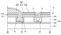
前記ホールを取り囲み、いずれもアンダーカット構造を有する少なくとも2つの溝と、を含み、
前記基板は、下方からこの順に積層された第1基板、第1無機層、第2基板及び第2無機層を含み、
前記少なくとも2つの溝は、いずれも、前記ディスプレイ層から前記第2基板までにわたって深さ方向に延長されたディスプレイ装置。 - 前記少なくとも2つの溝は、前記ホールと最も近接し、前記ホールと離隔された第1溝と、前記第1溝を取り囲み、前記第1溝と離隔された第2溝と、を含み、
前記第1無機層は、前記アンダーカット構造をなすように互いに対向して、前記第1溝内に突き出すように延長された1対の第1チップを含み、
前記第1無機層は、前記アンダーカット構造をなすように互いに対向して、前記第2溝内に突き出すように延長された1対の第2チップを含むことを特徴とする請求項1に記載のディスプレイ装置。 - 前記第2チップにおける、前記ホールに近い内側のものと、外側のものとを、部分的に連結するブリッジをさらに含み、
前記ブリッジは、前記1対の第2チップと一体であり、
前記第1チップは、前記ホールに近い内側のものと、外側のものとが、前記第1溝に沿った全体にわたって互いに離隔されたことを特徴とする請求項2に記載のディスプレイ装置。 - 前記ディスプレイ層を覆う封止層をさらに含み、
前記封止層は、下方からこの順に積層された第1無機封止層、有機封止層及び第2無機封止層を含み、
前記第1無機封止層は、前記第1溝及び前記第2溝の底面と内部の側壁面とを覆うことを特徴とする請求項3に記載のディスプレイ装置。 - 前記第1無機封止層は、前記ブリッジの下面を覆うことを特徴とする請求項4に記載のディスプレイ装置。
- 前記有機封止層は、前記第2溝に充填されたことを特徴とする請求項4に記載のディスプレイ装置。
- 前記第2無機封止層は、前記第1溝内にて、前記第1無機封止層と重ね合わされて接することを特徴とする請求項4に記載のディスプレイ装置。
- 前記第1無機封止層と前記第2無機封止層は、前記ホールの内部の側壁面にまで延長され、前記基板の側面と接することを特徴とする請求項7に記載のディスプレイ装置。
- 前記回路層は、薄膜トランジスタを含み、前記ディスプレイ層は、前記薄膜トランジスタと電気的に連結された有機発光素子を含むことを特徴とする請求項1に記載のディスプレイ装置。
- 順次に積層された第1基板、第1無機層、第2基板及び第2無機層を含む基板と、
前記基板上の回路層と、
前記回路層上のディスプレイ層と、
前記基板の表示領域内に位置して、前記基板、前記回路層及び前記ディスプレイ層を貫通する少なくとも1つのホールと、
前記基板の表示領域内に位置して、前記ホールを取り囲む第1溝及び第2溝と、
前記ディスプレイ層を覆う封止層と、を含み、
前記第2溝は、前記第1溝と離隔されて、前記第1溝を取り囲み、
前記封止層の有機封止層は、前記第2溝を充填するディスプレイ装置。 - 前記第1溝及び前記第2溝は、いずれも、前記ディスプレイ層から前記第2基板までにわたって深さ方向に延長されたことを特徴とする請求項10に記載のディスプレイ装置。
- 前記封止層は、前記有機封止層の下方及び上方に、それぞれ第1無機封止層と第2無機封止層とをさらに含み、
前記第1無機封止層と前記第2無機封止層とは、前記第1溝内で互いに重ね合わされて接することを特徴とする請求項11に記載のディスプレイ装置。 - 前記第1無機層は、前記ホールに近い内側と、外側とから、互いへと向かって、前記第1溝内に突き出すように延長された1対の第1チップを含み、
前記第1無機層は、前記ホールに近い内側と、外側とから、互いへと向かって、前記第2溝内に突き出すように延長された1対の第2チップを含むことを特徴とする請求項10に記載のディスプレイ装置。 - 前記第1溝及び前記第2溝は、いずれも、上部での幅が下部での幅より狭いことを特徴とする請求項13に記載のディスプレイ装置。
- 前記第1無機層は、前記第2溝に沿って配列されて、前記第2チップにおける、前記ホールに近い内側のものと、外側のものとを、部分的に互いに連結するブリッジをさらに含み、
前記第1チップは、前記ホールに近い内側のものと、外側のものとが、前記第1溝に沿った全体にわたって互いに離隔されたことを特徴とする請求項13に記載のディスプレイ装置。 - 前記第1無機層は、前記ブリッジを複数個含み、複数個の前記ブリッジは、前記第2溝に沿って互いに一定の間隔で離隔されて配列されたことを特徴とする請求項13に記載のディスプレイ装置。
- 前記回路層は、薄膜トランジスタを含み、前記ディスプレイ層は、前記薄膜トランジスタと電気的に連結された有機発光素子を含むことを特徴とする請求項10に記載のディスプレイ装置。
- 順次に積層された第1基板、第1無機層、第2基板及び第2無機層を含む基板と、
前記基板上の回路層と、
前記回路層上のディスプレイ層と、
前記基板の表示領域内に位置し、前記基板、前記回路層及び前記ディスプレイ層を貫通する少なくとも1つのホールと、
前記基板の表示領域内にて、前記ホールを取り囲む第1溝及び第2溝と、を含み、
前記第2無機層は、前記ホールに近い内側と、外側とから、互いへと向かって、前記第1溝内に突き出すように延長された1対の第1チップを含み、
前記第2無機層は、前記ホールに近い内側と、外側とから、互いへ向かって、前記第2溝内に突き出すように延長された1対の第2チップを含むディスプレイ装置。 - 前記第1溝及び前記第2溝は、いずれも、前記ディスプレイ層から前記第2基板までにわたって深さ方向に延長され、前記第2溝は、前記第1溝と離隔され、前記第1溝を取り囲むことを特徴とする請求項18に記載のディスプレイ装置。
- 前記ディスプレイ層を覆う封止層をさらに含み、
前記封止層は、前記第2溝を充填する有機封止層、並びに前記有機封止層の下方と上方とにそれぞれ位置する第1無機封止層及び第2無機封止層を含み、
前記第1無機封止層と前記第2無機封止層とは、前記第1溝内にて、互いに重ね合わされて接することを特徴とする請求項18に記載のディスプレイ装置。
Applications Claiming Priority (2)
| Application Number | Priority Date | Filing Date | Title |
|---|---|---|---|
| KR1020180075579A KR20200003328A (ko) | 2018-06-29 | 2018-06-29 | 디스플레이 장치 |
| KR10-2018-0075579 | 2018-06-29 |
Publications (2)
| Publication Number | Publication Date |
|---|---|
| JP2020004705A true JP2020004705A (ja) | 2020-01-09 |
| JP7301579B2 JP7301579B2 (ja) | 2023-07-03 |
Family
ID=67180515
Family Applications (1)
| Application Number | Title | Priority Date | Filing Date |
|---|---|---|---|
| JP2019068430A Active JP7301579B2 (ja) | 2018-06-29 | 2019-03-29 | ディスプレイ装置 |
Country Status (5)
| Country | Link |
|---|---|
| US (4) | US10930885B2 (ja) |
| EP (1) | EP3588574B1 (ja) |
| JP (1) | JP7301579B2 (ja) |
| KR (1) | KR20200003328A (ja) |
| CN (1) | CN110660828A (ja) |
Cited By (3)
| Publication number | Priority date | Publication date | Assignee | Title |
|---|---|---|---|---|
| WO2021205603A1 (ja) * | 2020-04-09 | 2021-10-14 | シャープ株式会社 | 表示装置及びその製造方法 |
| KR20220057434A (ko) | 2020-10-29 | 2022-05-09 | 도쿄엘렉트론가부시키가이샤 | 유기 el 패널의 제조 방법 및 유기 el 패널 |
| WO2022224073A1 (ja) * | 2021-04-23 | 2022-10-27 | 株式会社半導体エネルギー研究所 | 表示装置、及び表示装置の作製方法 |
Families Citing this family (23)
| Publication number | Priority date | Publication date | Assignee | Title |
|---|---|---|---|---|
| KR20190108212A (ko) | 2018-03-13 | 2019-09-24 | 삼성디스플레이 주식회사 | 표시 패널 및 이를 포함하는 표시 장치의 제조 방법 |
| KR20200003328A (ko) | 2018-06-29 | 2020-01-09 | 삼성디스플레이 주식회사 | 디스플레이 장치 |
| KR102548987B1 (ko) | 2018-08-09 | 2023-06-29 | 삼성디스플레이 주식회사 | 디스플레이 장치 |
| KR102626939B1 (ko) * | 2018-10-05 | 2024-01-19 | 삼성디스플레이 주식회사 | 표시 장치 |
| KR102653262B1 (ko) | 2018-10-16 | 2024-04-01 | 삼성전자 주식회사 | 개구부가 형성된 터치 레이어를 포함하는 전자 장치 |
| CN110164916B (zh) * | 2018-12-05 | 2021-02-02 | 京东方科技集团股份有限公司 | 显示面板、显示设备及制造显示面板的方法 |
| KR102168042B1 (ko) * | 2018-12-27 | 2020-10-20 | 엘지디스플레이 주식회사 | 표시 장치 |
| KR20200126451A (ko) | 2019-04-29 | 2020-11-09 | 삼성디스플레이 주식회사 | 전자 장치 |
| KR20200145954A (ko) * | 2019-06-21 | 2020-12-31 | 삼성디스플레이 주식회사 | 표시 장치 |
| CN110335964B (zh) * | 2019-06-26 | 2020-11-10 | 武汉华星光电半导体显示技术有限公司 | 一种显示面板 |
| KR20210010778A (ko) * | 2019-07-19 | 2021-01-28 | 삼성디스플레이 주식회사 | 플렉서블 디스플레이 장치 |
| CN110265583B (zh) * | 2019-07-26 | 2022-08-12 | 京东方科技集团股份有限公司 | 一种显示面板及其制备方法、显示装置 |
| CN111192974B (zh) * | 2020-01-07 | 2022-07-12 | 武汉华星光电半导体显示技术有限公司 | 阵列基板及其制备方法 |
| CN111244322B (zh) * | 2020-01-17 | 2022-04-26 | 京东方科技集团股份有限公司 | 显示基板及其制作方法、和显示装置 |
| CN111627930B (zh) * | 2020-05-27 | 2022-09-09 | 武汉华星光电半导体显示技术有限公司 | 阵列基板及其制备方法与显示面板 |
| CN111834546A (zh) * | 2020-07-07 | 2020-10-27 | 武汉华星光电半导体显示技术有限公司 | 显示装置、显示面板及其制作方法 |
| US11600800B2 (en) * | 2020-07-31 | 2023-03-07 | Innolux Corporation | Electronic device having a curved profile interface corresponding to a recess |
| CN112599701B (zh) * | 2020-12-14 | 2022-05-17 | 合肥维信诺科技有限公司 | 显示基板 |
| CN112820742A (zh) * | 2021-01-19 | 2021-05-18 | 合肥维信诺科技有限公司 | 显示面板的制备方法和显示面板 |
| CN113193015B (zh) * | 2021-04-16 | 2022-07-12 | 武汉华星光电技术有限公司 | 显示面板及其制备方法、显示装置 |
| CN113192983B (zh) * | 2021-04-19 | 2022-12-06 | 武汉华星光电半导体显示技术有限公司 | 显示面板及其制备方法 |
| CN114613923A (zh) * | 2022-03-14 | 2022-06-10 | 武汉华星光电半导体显示技术有限公司 | 显示面板及显示装置 |
| CN114824127B (zh) * | 2022-04-06 | 2023-04-07 | 武汉华星光电半导体显示技术有限公司 | 显示面板及其制作方法 |
Citations (6)
| Publication number | Priority date | Publication date | Assignee | Title |
|---|---|---|---|---|
| JP2011008969A (ja) * | 2009-06-23 | 2011-01-13 | Canon Inc | 表示装置 |
| US20160190389A1 (en) * | 2014-12-26 | 2016-06-30 | Samsung Display Co., Ltd. | Display device and method of manufacturing the same |
| US20170031323A1 (en) * | 2015-07-29 | 2017-02-02 | Lg Display Co., Ltd. | Organic light emitting display device |
| US20170148856A1 (en) * | 2015-11-20 | 2017-05-25 | Samsung Display Co., Ltd | Organic light-emitting display and method of manufacturing the same |
| KR20170059864A (ko) * | 2015-11-20 | 2017-05-31 | 삼성디스플레이 주식회사 | 유기 발광 표시 장치 및 그 제조 방법 |
| US20180151834A1 (en) * | 2016-11-28 | 2018-05-31 | Japan Display Inc. | Display device |
Family Cites Families (16)
| Publication number | Priority date | Publication date | Assignee | Title |
|---|---|---|---|---|
| KR101137389B1 (ko) * | 2009-12-15 | 2012-04-20 | 삼성모바일디스플레이주식회사 | 플렉서블 디스플레이용 기판, 이를 제조하는 방법, 및 이 기판제조방법을 이용한 유기 발광 디스플레이 장치의 제조 방법 |
| KR101801913B1 (ko) | 2012-03-23 | 2017-11-28 | 삼성디스플레이 주식회사 | 유기 발광 디스플레이 장치와, 이의 제조 방법 |
| TWI637949B (zh) | 2013-06-14 | 2018-10-11 | 塩野義製藥股份有限公司 | 胺基三衍生物及含有其等之醫藥組合物 |
| KR102391361B1 (ko) * | 2015-01-14 | 2022-04-27 | 삼성디스플레이 주식회사 | 유기 발광 표시 장치 |
| KR20170015832A (ko) | 2015-08-01 | 2017-02-09 | 이승범 | 버켓 자동 회전 기능을 갖는 외발 자전거 형태의 제설장치 |
| KR20170069864A (ko) | 2015-12-13 | 2017-06-21 | 배도연 | 지하철 요금 자동 결제 개찰구 |
| JP6646473B2 (ja) | 2016-02-25 | 2020-02-14 | 株式会社ジャパンディスプレイ | 表示装置、表示装置の製造方法 |
| KR101766352B1 (ko) | 2016-03-10 | 2017-08-09 | (주)하드램 | 유연소자용 다파장 선택적 레이저 커팅 시스템 |
| KR102421577B1 (ko) | 2016-04-05 | 2022-07-18 | 삼성디스플레이 주식회사 | 디스플레이 장치 |
| KR102605208B1 (ko) * | 2016-06-28 | 2023-11-24 | 삼성디스플레이 주식회사 | 유기 발광 표시 장치 및 유기 발광 표시 장치의 제조 방법 |
| KR102448325B1 (ko) | 2017-11-16 | 2022-09-30 | 삼성디스플레이 주식회사 | 표시패널 및 이를 포함하는 전자장치 |
| EP3488962A1 (en) | 2017-11-28 | 2019-05-29 | Vestel Elektronik Sanayi ve Ticaret A.S. | Solder composition and method of soldering |
| KR102520016B1 (ko) * | 2018-02-02 | 2023-04-11 | 삼성디스플레이 주식회사 | 표시 패널 및 이를 포함하는 전자 장치 |
| KR102583898B1 (ko) * | 2018-04-30 | 2023-10-04 | 삼성디스플레이 주식회사 | 표시 패널 및 이의 제조 방법 |
| KR20200003328A (ko) * | 2018-06-29 | 2020-01-09 | 삼성디스플레이 주식회사 | 디스플레이 장치 |
| KR102612036B1 (ko) * | 2018-09-27 | 2023-12-11 | 삼성디스플레이 주식회사 | 표시 패널 및 이를 포함한 전자 장치 |
-
2018
- 2018-06-29 KR KR1020180075579A patent/KR20200003328A/ko not_active Application Discontinuation
-
2019
- 2019-03-29 JP JP2019068430A patent/JP7301579B2/ja active Active
- 2019-05-21 US US16/418,578 patent/US10930885B2/en active Active
- 2019-06-26 CN CN201910558894.9A patent/CN110660828A/zh active Pending
- 2019-06-28 EP EP19183255.9A patent/EP3588574B1/en active Active
-
2021
- 2021-02-22 US US17/182,120 patent/US11462717B2/en active Active
-
2022
- 2022-10-04 US US17/959,986 patent/US11839105B2/en active Active
-
2023
- 2023-11-07 US US18/504,140 patent/US20240074228A1/en active Pending
Patent Citations (7)
| Publication number | Priority date | Publication date | Assignee | Title |
|---|---|---|---|---|
| JP2011008969A (ja) * | 2009-06-23 | 2011-01-13 | Canon Inc | 表示装置 |
| US20160190389A1 (en) * | 2014-12-26 | 2016-06-30 | Samsung Display Co., Ltd. | Display device and method of manufacturing the same |
| US20170031323A1 (en) * | 2015-07-29 | 2017-02-02 | Lg Display Co., Ltd. | Organic light emitting display device |
| US20170148856A1 (en) * | 2015-11-20 | 2017-05-25 | Samsung Display Co., Ltd | Organic light-emitting display and method of manufacturing the same |
| KR20170059864A (ko) * | 2015-11-20 | 2017-05-31 | 삼성디스플레이 주식회사 | 유기 발광 표시 장치 및 그 제조 방법 |
| US20180151834A1 (en) * | 2016-11-28 | 2018-05-31 | Japan Display Inc. | Display device |
| JP2018087863A (ja) * | 2016-11-28 | 2018-06-07 | 株式会社ジャパンディスプレイ | 表示装置 |
Cited By (3)
| Publication number | Priority date | Publication date | Assignee | Title |
|---|---|---|---|---|
| WO2021205603A1 (ja) * | 2020-04-09 | 2021-10-14 | シャープ株式会社 | 表示装置及びその製造方法 |
| KR20220057434A (ko) | 2020-10-29 | 2022-05-09 | 도쿄엘렉트론가부시키가이샤 | 유기 el 패널의 제조 방법 및 유기 el 패널 |
| WO2022224073A1 (ja) * | 2021-04-23 | 2022-10-27 | 株式会社半導体エネルギー研究所 | 表示装置、及び表示装置の作製方法 |
Also Published As
| Publication number | Publication date |
|---|---|
| US10930885B2 (en) | 2021-02-23 |
| US11839105B2 (en) | 2023-12-05 |
| EP3588574B1 (en) | 2021-11-03 |
| KR20200003328A (ko) | 2020-01-09 |
| JP7301579B2 (ja) | 2023-07-03 |
| CN110660828A (zh) | 2020-01-07 |
| US20200006700A1 (en) | 2020-01-02 |
| US20230026398A1 (en) | 2023-01-26 |
| EP3588574A1 (en) | 2020-01-01 |
| US20210175472A1 (en) | 2021-06-10 |
| US20240074228A1 (en) | 2024-02-29 |
| US11462717B2 (en) | 2022-10-04 |
Similar Documents
| Publication | Publication Date | Title |
|---|---|---|
| JP7301579B2 (ja) | ディスプレイ装置 | |
| KR102548987B1 (ko) | 디스플레이 장치 | |
| KR102611205B1 (ko) | 유기 발광 표시 장치 | |
| US11081668B2 (en) | Display device | |
| KR102602191B1 (ko) | 디스플레이 장치 | |
| CN106252379B (zh) | 显示装置 | |
| KR102541447B1 (ko) | 유기 발광 표시 장치 | |
| TW201740257A (zh) | 顯示設備及其製造方法 | |
| KR20160110598A (ko) | 유기 발광 표시 장치 | |
| KR20210109715A (ko) | 디스플레이 장치의 제조방법 | |
| KR20200144627A (ko) | 디스플레이 장치 및 이의 제조 방법 | |
| KR102637790B1 (ko) | 디스플레이 장치 및 이의 제조 방법 | |
| US20210036197A1 (en) | Display apparatus having a substrate hole | |
| KR102671040B1 (ko) | 디스플레이 장치 |
Legal Events
| Date | Code | Title | Description |
|---|---|---|---|
| A621 | Written request for application examination |
Free format text: JAPANESE INTERMEDIATE CODE: A621 Effective date: 20220218 |
|
| A977 | Report on retrieval |
Free format text: JAPANESE INTERMEDIATE CODE: A971007 Effective date: 20221019 |
|
| A131 | Notification of reasons for refusal |
Free format text: JAPANESE INTERMEDIATE CODE: A131 Effective date: 20221101 |
|
| A521 | Request for written amendment filed |
Free format text: JAPANESE INTERMEDIATE CODE: A523 Effective date: 20230131 |
|
| A131 | Notification of reasons for refusal |
Free format text: JAPANESE INTERMEDIATE CODE: A131 Effective date: 20230221 |
|
| A521 | Request for written amendment filed |
Free format text: JAPANESE INTERMEDIATE CODE: A523 Effective date: 20230512 |
|
| TRDD | Decision of grant or rejection written | ||
| A01 | Written decision to grant a patent or to grant a registration (utility model) |
Free format text: JAPANESE INTERMEDIATE CODE: A01 Effective date: 20230530 |
|
| A61 | First payment of annual fees (during grant procedure) |
Free format text: JAPANESE INTERMEDIATE CODE: A61 Effective date: 20230621 |
|
| R150 | Certificate of patent or registration of utility model |
Ref document number: 7301579 Country of ref document: JP Free format text: JAPANESE INTERMEDIATE CODE: R150 |