JP2017004586A - 磁気抵抗センサ製造 - Google Patents
磁気抵抗センサ製造 Download PDFInfo
- Publication number
- JP2017004586A JP2017004586A JP2016075042A JP2016075042A JP2017004586A JP 2017004586 A JP2017004586 A JP 2017004586A JP 2016075042 A JP2016075042 A JP 2016075042A JP 2016075042 A JP2016075042 A JP 2016075042A JP 2017004586 A JP2017004586 A JP 2017004586A
- Authority
- JP
- Japan
- Prior art keywords
- layer
- reader
- shield
- saf
- shield structure
- Prior art date
- Legal status (The legal status is an assumption and is not a legal conclusion. Google has not performed a legal analysis and makes no representation as to the accuracy of the status listed.)
- Pending
Links
- 238000004519 manufacturing process Methods 0.000 title description 6
- 229910001030 Iron–nickel alloy Inorganic materials 0.000 claims abstract description 28
- 230000005290 antiferromagnetic effect Effects 0.000 claims abstract description 25
- 239000000696 magnetic material Substances 0.000 claims abstract description 25
- 230000008878 coupling Effects 0.000 claims abstract description 24
- 238000010168 coupling process Methods 0.000 claims abstract description 24
- 238000005859 coupling reaction Methods 0.000 claims abstract description 24
- 239000000654 additive Substances 0.000 claims abstract description 22
- 230000000996 additive effect Effects 0.000 claims abstract description 19
- 238000003780 insertion Methods 0.000 claims abstract description 17
- 230000037431 insertion Effects 0.000 claims abstract description 17
- 239000012535 impurity Substances 0.000 claims abstract description 16
- 239000000463 material Substances 0.000 claims description 20
- 229910045601 alloy Inorganic materials 0.000 claims description 8
- 239000000956 alloy Substances 0.000 claims description 8
- 229910019236 CoFeB Inorganic materials 0.000 claims description 7
- 239000010955 niobium Substances 0.000 claims description 6
- 229910052715 tantalum Inorganic materials 0.000 claims description 5
- 229910052735 hafnium Inorganic materials 0.000 claims description 4
- VBJZVLUMGGDVMO-UHFFFAOYSA-N hafnium atom Chemical compound [Hf] VBJZVLUMGGDVMO-UHFFFAOYSA-N 0.000 claims description 4
- 239000003779 heat-resistant material Substances 0.000 claims description 4
- 229910052758 niobium Inorganic materials 0.000 claims description 4
- GUCVJGMIXFAOAE-UHFFFAOYSA-N niobium atom Chemical compound [Nb] GUCVJGMIXFAOAE-UHFFFAOYSA-N 0.000 claims description 4
- GUVRBAGPIYLISA-UHFFFAOYSA-N tantalum atom Chemical compound [Ta] GUVRBAGPIYLISA-UHFFFAOYSA-N 0.000 claims description 4
- QVGXLLKOCUKJST-UHFFFAOYSA-N atomic oxygen Chemical group [O] QVGXLLKOCUKJST-UHFFFAOYSA-N 0.000 claims description 2
- 229910052760 oxygen Inorganic materials 0.000 claims description 2
- 239000001301 oxygen Substances 0.000 claims description 2
- WFKWXMTUELFFGS-UHFFFAOYSA-N tungsten Chemical group [W] WFKWXMTUELFFGS-UHFFFAOYSA-N 0.000 claims description 2
- 229910052721 tungsten Inorganic materials 0.000 claims description 2
- 239000010937 tungsten Substances 0.000 claims description 2
- 239000002131 composite material Substances 0.000 claims 8
- QCWXUUIWCKQGHC-UHFFFAOYSA-N Zirconium Chemical compound [Zr] QCWXUUIWCKQGHC-UHFFFAOYSA-N 0.000 claims 2
- 239000003795 chemical substances by application Substances 0.000 claims 2
- 229910052726 zirconium Inorganic materials 0.000 claims 2
- ZOXJGFHDIHLPTG-UHFFFAOYSA-N Boron Chemical compound [B] ZOXJGFHDIHLPTG-UHFFFAOYSA-N 0.000 claims 1
- 229910000531 Co alloy Inorganic materials 0.000 claims 1
- 229910000640 Fe alloy Inorganic materials 0.000 claims 1
- 229910000990 Ni alloy Inorganic materials 0.000 claims 1
- 229910052796 boron Inorganic materials 0.000 claims 1
- 230000005291 magnetic effect Effects 0.000 abstract description 52
- 238000000137 annealing Methods 0.000 abstract description 20
- 230000015556 catabolic process Effects 0.000 abstract description 16
- 238000006731 degradation reaction Methods 0.000 abstract description 16
- 230000015572 biosynthetic process Effects 0.000 abstract description 7
- 230000001808 coupling effect Effects 0.000 abstract 1
- 229910003321 CoFe Inorganic materials 0.000 description 14
- 230000005415 magnetization Effects 0.000 description 14
- 238000000034 method Methods 0.000 description 11
- 125000006850 spacer group Chemical group 0.000 description 9
- 230000004907 flux Effects 0.000 description 7
- 230000008569 process Effects 0.000 description 6
- 230000009977 dual effect Effects 0.000 description 5
- 239000000758 substrate Substances 0.000 description 5
- 238000010438 heat treatment Methods 0.000 description 4
- 239000011819 refractory material Substances 0.000 description 4
- 230000004044 response Effects 0.000 description 4
- 230000006641 stabilisation Effects 0.000 description 4
- 238000011105 stabilization Methods 0.000 description 4
- 238000002955 isolation Methods 0.000 description 3
- 229910052751 metal Inorganic materials 0.000 description 3
- 239000002184 metal Substances 0.000 description 3
- 230000008859 change Effects 0.000 description 2
- VNNRSPGTAMTISX-UHFFFAOYSA-N chromium nickel Chemical compound [Cr].[Ni] VNNRSPGTAMTISX-UHFFFAOYSA-N 0.000 description 2
- 230000000694 effects Effects 0.000 description 2
- 239000003302 ferromagnetic material Substances 0.000 description 2
- 239000010408 film Substances 0.000 description 2
- 230000006872 improvement Effects 0.000 description 2
- XEEYBQQBJWHFJM-UHFFFAOYSA-N iron Substances [Fe] XEEYBQQBJWHFJM-UHFFFAOYSA-N 0.000 description 2
- 229910001120 nichrome Inorganic materials 0.000 description 2
- 238000000059 patterning Methods 0.000 description 2
- VSZWPYCFIRKVQL-UHFFFAOYSA-N selanylidenegallium;selenium Chemical compound [Se].[Se]=[Ga].[Se]=[Ga] VSZWPYCFIRKVQL-UHFFFAOYSA-N 0.000 description 2
- RYGMFSIKBFXOCR-UHFFFAOYSA-N Copper Chemical compound [Cu] RYGMFSIKBFXOCR-UHFFFAOYSA-N 0.000 description 1
- KJTLSVCANCCWHF-UHFFFAOYSA-N Ruthenium Chemical compound [Ru] KJTLSVCANCCWHF-UHFFFAOYSA-N 0.000 description 1
- 230000004888 barrier function Effects 0.000 description 1
- 230000009286 beneficial effect Effects 0.000 description 1
- 239000010941 cobalt Substances 0.000 description 1
- 229910017052 cobalt Inorganic materials 0.000 description 1
- GUTLYIVDDKVIGB-UHFFFAOYSA-N cobalt atom Chemical compound [Co] GUTLYIVDDKVIGB-UHFFFAOYSA-N 0.000 description 1
- 229910052802 copper Inorganic materials 0.000 description 1
- 239000010949 copper Substances 0.000 description 1
- 239000013078 crystal Substances 0.000 description 1
- 238000013500 data storage Methods 0.000 description 1
- 238000010586 diagram Methods 0.000 description 1
- 238000009792 diffusion process Methods 0.000 description 1
- 238000005516 engineering process Methods 0.000 description 1
- 238000011066 ex-situ storage Methods 0.000 description 1
- 230000005294 ferromagnetic effect Effects 0.000 description 1
- 238000011065 in-situ storage Methods 0.000 description 1
- 230000002401 inhibitory effect Effects 0.000 description 1
- 229910052742 iron Inorganic materials 0.000 description 1
- 230000007246 mechanism Effects 0.000 description 1
- 150000002739 metals Chemical class 0.000 description 1
- 238000011084 recovery Methods 0.000 description 1
- 230000000717 retained effect Effects 0.000 description 1
- 229910052707 ruthenium Inorganic materials 0.000 description 1
- 230000035945 sensitivity Effects 0.000 description 1
- 238000000926 separation method Methods 0.000 description 1
- 239000007787 solid Substances 0.000 description 1
- 238000004544 sputter deposition Methods 0.000 description 1
- 238000003860 storage Methods 0.000 description 1
- 238000005728 strengthening Methods 0.000 description 1
- 239000010409 thin film Substances 0.000 description 1
Images


Classifications
-
- G—PHYSICS
- G11—INFORMATION STORAGE
- G11B—INFORMATION STORAGE BASED ON RELATIVE MOVEMENT BETWEEN RECORD CARRIER AND TRANSDUCER
- G11B5/00—Recording by magnetisation or demagnetisation of a record carrier; Reproducing by magnetic means; Record carriers therefor
- G11B5/127—Structure or manufacture of heads, e.g. inductive
- G11B5/33—Structure or manufacture of flux-sensitive heads, i.e. for reproduction only; Combination of such heads with means for recording or erasing only
- G11B5/39—Structure or manufacture of flux-sensitive heads, i.e. for reproduction only; Combination of such heads with means for recording or erasing only using magneto-resistive devices or effects
- G11B5/3903—Structure or manufacture of flux-sensitive heads, i.e. for reproduction only; Combination of such heads with means for recording or erasing only using magneto-resistive devices or effects using magnetic thin film layers or their effects, the films being part of integrated structures
- G11B5/3906—Details related to the use of magnetic thin film layers or to their effects
- G11B5/3912—Arrangements in which the active read-out elements are transducing in association with active magnetic shields, e.g. magnetically coupled shields
-
- G—PHYSICS
- G11—INFORMATION STORAGE
- G11B—INFORMATION STORAGE BASED ON RELATIVE MOVEMENT BETWEEN RECORD CARRIER AND TRANSDUCER
- G11B5/00—Recording by magnetisation or demagnetisation of a record carrier; Reproducing by magnetic means; Record carriers therefor
- G11B5/127—Structure or manufacture of heads, e.g. inductive
- G11B5/33—Structure or manufacture of flux-sensitive heads, i.e. for reproduction only; Combination of such heads with means for recording or erasing only
- G11B5/39—Structure or manufacture of flux-sensitive heads, i.e. for reproduction only; Combination of such heads with means for recording or erasing only using magneto-resistive devices or effects
- G11B5/3903—Structure or manufacture of flux-sensitive heads, i.e. for reproduction only; Combination of such heads with means for recording or erasing only using magneto-resistive devices or effects using magnetic thin film layers or their effects, the films being part of integrated structures
- G11B5/3967—Composite structural arrangements of transducers, e.g. inductive write and magnetoresistive read
- G11B5/397—Composite structural arrangements of transducers, e.g. inductive write and magnetoresistive read with a plurality of independent magnetoresistive active read-out elements for respectively transducing from selected components
- G11B5/3974—Composite structural arrangements of transducers, e.g. inductive write and magnetoresistive read with a plurality of independent magnetoresistive active read-out elements for respectively transducing from selected components from the same information track, e.g. frequency bands
-
- G—PHYSICS
- G11—INFORMATION STORAGE
- G11B—INFORMATION STORAGE BASED ON RELATIVE MOVEMENT BETWEEN RECORD CARRIER AND TRANSDUCER
- G11B5/00—Recording by magnetisation or demagnetisation of a record carrier; Reproducing by magnetic means; Record carriers therefor
- G11B5/127—Structure or manufacture of heads, e.g. inductive
- G11B5/33—Structure or manufacture of flux-sensitive heads, i.e. for reproduction only; Combination of such heads with means for recording or erasing only
- G11B5/39—Structure or manufacture of flux-sensitive heads, i.e. for reproduction only; Combination of such heads with means for recording or erasing only using magneto-resistive devices or effects
- G11B5/3903—Structure or manufacture of flux-sensitive heads, i.e. for reproduction only; Combination of such heads with means for recording or erasing only using magneto-resistive devices or effects using magnetic thin film layers or their effects, the films being part of integrated structures
- G11B5/398—Specially shaped layers
Abstract
Description
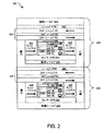
磁気データ記憶検索システムでは、磁気読取/書込ヘッドは、磁気ディスクに記憶される磁気的にエンコードされた情報を検索するために磁気抵抗(MR)センサを有するリーダ部分を含む。ディスクの表面からの磁束は、MRセンサの感知層の磁化ベクトルの回転を引起し、それは、次いで、MRセンサの電気固有抵抗における変化を引起す。MRセンサの抵抗率における変化は、MRセンサを通して電流を流し、MRセンサにわたる電圧変化を測定することによって、検出することができる。次いで、外部回路系が、電圧情報を適切なフォーマットに変換し、その情報を操作して、ディスク上にエンコードされた情報を回復する。
ここに記載され主張される実現例はリーダ構造を含み、リーダ構造は、センサスタックを含む第1のリーダと、頂部シールド構造とを含み、頂部シールド構造は合成反強磁性(SAF)シールド構造を含み、合成反強磁性(SAF)シールド構造は、少なくともNiFeの層と不純物添加物とを含む基準層(RL)と、RKKY結合層(たとえばRu層)と、固定(pinned)層(PL)とを含む。他の実現例では、第1のリーダのSAFシールド構造のRLは、少なくとも非晶質の磁性材料の層を含む。しかし、他の実現例では、SAFシールド構造は、非晶質の磁性材料の挿入層を、SAFシールドRL下、SAFシールドRL内、またはSAFシールドRLとSAFシールドRuとの間に含む。
磁気媒体からデータを読出すために、高データ密度および感度のよいセンサに対して増大する要求がある。増大した感度を有する巨大磁気抵抗センサ(GMRセンサ)は、銅などのような薄い導電性の非磁性スペーサ層によって分離された2つの軟磁性層からなる。トンネル磁気抵抗センサ(TMRセンサ)は、GMRセンサに拡張を与え、そこでは、電子が、それらのスピンが薄い絶縁トンネル障壁を横切って好ましい方向に配向される状態で、移動する。
Claims (20)
- リーダ構造であって、
第1のリーダを含み、前記第1のリーダは、
センサスタックと、
頂部シールド構造とを含み、前記頂部シールド構造は、合成反強磁性シールド構造を含み、前記合成反強磁性シールド構造は、
少なくともNiFeの層と不純物添加物とを含む基準層と、
RKKY結合層と、
固定層とを含む、リーダ構造。 - 前記第1のリーダからダウントラック方向において位置決めされる第2のリーダをさらに含み、前記第2のリーダは、
センサスタックと、
頂部シールド構造とを含み、前記頂部シールド構造は、合成反強磁性シールド構造を含み、前記合成反強磁性シールド構造は、
少なくともNiFeの層と不純物添加物とを含む基準層と、
RKKY結合層と、
固定層とを含む、請求項1に記載のリーダ構造。 - 前記不純物添加物は酸素である、請求項1に記載のリーダ構造。
- 前記不純物添加物はタングステン(W)である、請求項1に記載のリーダ構造。
- 前記基準層におけるWの含有量は14原子百分率未満である、請求項4に記載のリーダ構造。
- 前記不純物添加物は耐熱性材料である、請求項1に記載のリーダ構造。
- 前記耐熱性材料はタンタル、ニオブ、ハフニウムおよびジルコニウムの少なくとも1つである、請求項6に記載のリーダ構造。
- 前記RKKY結合層は約0〜20Åの範囲に厚みを有する、請求項1に記載のリーダ構造。
- リーダ構造であって、
第1のリーダを含み、前記第1のリーダは、
センサスタックと、
頂部シールド構造とを含み、前記頂部シールド構造は、合成反強磁性構造を含み、前記合成反強磁性構造は、
少なくとも非晶質の磁性材料の層を含む基準層と、
RKKY結合層と、
固定層とを含む、リーダ構造。 - 前記第1のリーダからダウントラック方向において位置決めされる第2のリーダをさらに含み、前記第2のリーダは、
センサスタックと、
頂部シールド構造とを含み、前記頂部シールド構造は、合成反強磁性シールド構造を含み、前記合成反強磁性シールド構造は、
少なくともNiFeの層と不純物添加物とを含む基準層と、
RKKY結合層と、
固定層とを含む、請求項9に記載のリーダ構造。 - 前記非晶質の磁性材料は、合金を非晶質の作用剤でドープすることによって形成される、請求項9に記載のリーダ構造。
- 前記合金はニッケル合金、コバルト合金および鉄合金の少なくとも1つである、請求項11に記載のリーダ構造。
- 前記非晶質の作用剤は、タンタル、ホウ素、ハフニウム、ジルコニウムおよびニオブの少なくとも1つを含む、請求項11に記載のリーダ構造。
- リーダ構造であって、
第1のリーダを含み、前記第1のリーダは、
センサスタックと、
頂部シールド構造とを含み、前記頂部シールド構造は、合成反強磁性構造を含み、前記合成反強磁性構造は、
挿入層と、
少なくともNiFeの層と不純物添加物とを含む基準層と、
RKKY結合層と、
固定層とを含む、リーダ構造。 - 前記第1のリーダからダウントラック方向において位置決めされる第2のリーダをさらに含み、前記第2のリーダは、
センサスタックと、
頂部シールド構造とを含み、前記頂部シールド構造は、合成反強磁性シールド構造を含み、前記合成反強磁性シールド構造は、
少なくともNiFeの層と不純物添加物とを含む基準層と、
RKKY結合層と、
固定層とを含む、請求項12に記載のリーダ構造。 - 前記不純物添加物はOである、請求項14に記載のリーダ構造。
- 前記不純物添加物はWである、請求項14に記載のリーダ構造。
- 前記不純物添加物は耐熱性材料である、請求項14に記載のリーダ構造。
- 前記挿入層は非晶質材料である、請求項14に記載のリーダ構造。
- 前記非晶質材料はTa、CoFeBおよびCoFeTaの少なくとも1つを含む、請求項19に記載のリーダ構造。
Applications Claiming Priority (2)
| Application Number | Priority Date | Filing Date | Title |
|---|---|---|---|
| US14/740,116 US20160365104A1 (en) | 2015-06-15 | 2015-06-15 | Magnetoresistive sensor fabrication |
| US14/740,116 | 2015-06-15 |
Publications (2)
| Publication Number | Publication Date |
|---|---|
| JP2017004586A true JP2017004586A (ja) | 2017-01-05 |
| JP2017004586A5 JP2017004586A5 (ja) | 2019-04-25 |
Family
ID=57516033
Family Applications (1)
| Application Number | Title | Priority Date | Filing Date |
|---|---|---|---|
| JP2016075042A Pending JP2017004586A (ja) | 2015-06-15 | 2016-04-04 | 磁気抵抗センサ製造 |
Country Status (2)
| Country | Link |
|---|---|
| US (2) | US20160365104A1 (ja) |
| JP (1) | JP2017004586A (ja) |
Cited By (1)
| Publication number | Priority date | Publication date | Assignee | Title |
|---|---|---|---|---|
| US11453170B2 (en) | 2017-08-31 | 2022-09-27 | General Electric Company | Distribution of customized engineering models for additive manufacturing |
Families Citing this family (6)
| Publication number | Priority date | Publication date | Assignee | Title |
|---|---|---|---|---|
| US9431031B1 (en) * | 2015-03-24 | 2016-08-30 | Western Digital (Fremont), Llc | System and method for magnetic transducers having multiple sensors and AFC shields |
| US20160365104A1 (en) * | 2015-06-15 | 2016-12-15 | Seagate Technology Llc | Magnetoresistive sensor fabrication |
| EP3442042B1 (en) * | 2017-08-10 | 2020-12-09 | Commissariat à l'Energie Atomique et aux Energies Alternatives | Synthetic antiferromagnetic layer, magnetic tunnel junction and spintronic device using said synthetic antiferromagnetic layer |
| US10614838B2 (en) | 2018-08-23 | 2020-04-07 | Seagate Technology Llc | Reader with side shields decoupled from a top shield |
| US11120933B1 (en) | 2019-03-29 | 2021-09-14 | Seagate Technology Llc | Stack cap with a non-magnetic layer including ferromagnetic elements |
| US10783907B1 (en) * | 2019-09-04 | 2020-09-22 | Seagate Technology Llc | Reader with bi-layered side shields |
Citations (8)
| Publication number | Priority date | Publication date | Assignee | Title |
|---|---|---|---|---|
| JP2002529926A (ja) * | 1998-11-09 | 2002-09-10 | インターナショナル・ビジネス・マシーンズ・コーポレーション | 磁気トンネル接合センサを使用するサーマル・アスペリティ低減回路を有するディスク・ドライブ |
| JP2008288235A (ja) * | 2007-05-15 | 2008-11-27 | Tdk Corp | 磁気検出素子及びその製造方法 |
| JP2009272031A (ja) * | 2008-05-09 | 2009-11-19 | Headway Technologies Inc | 磁気再生記録ヘッドおよびその製造方法 |
| JP2009283499A (ja) * | 2008-05-19 | 2009-12-03 | Toshiba Corp | 磁気抵抗効果素子、磁気抵抗効果ヘッド、磁気記録再生装置および磁気メモリ |
| JP2009290225A (ja) * | 2009-07-24 | 2009-12-10 | Toshiba Corp | 磁気抵抗効果素子,および磁気抵抗効果素子の製造方法 |
| JP2013008439A (ja) * | 2011-06-23 | 2013-01-10 | Seagate Technology Llc | センサ積層体、シールド、および第1のシールド安定化構造を備える装置、センサ積層体、シールド、および磁性層を備える装置、データ記憶媒体、記録ヘッド、およびアームを備える装置、ならびに、センサ構造を設け、これをアニールするステップを備える方法 |
| US8873204B1 (en) * | 2014-07-25 | 2014-10-28 | HGST Netherlands B.V. | Current-perpendicular-to-the-plane (CPP) magnetoresistive (MR) sensor structure with multiple stacked sensors and center shield with CoFeB insertion layer |
| JP2015028832A (ja) * | 2013-07-30 | 2015-02-12 | シーゲイト テクノロジー エルエルシー | 磁気抵抗性センサシールド |
Family Cites Families (36)
| Publication number | Priority date | Publication date | Assignee | Title |
|---|---|---|---|---|
| JPS59136444A (ja) * | 1983-01-24 | 1984-08-06 | Sony Corp | 非晶質磁性合金 |
| US6587315B1 (en) * | 1999-01-20 | 2003-07-01 | Alps Electric Co., Ltd. | Magnetoresistive-effect device with a magnetic coupling junction |
| JP2002076472A (ja) * | 2000-08-31 | 2002-03-15 | Alps Electric Co Ltd | スピンバルブ型薄膜磁気素子およびこのスピンバルブ型薄膜磁気素子を備えた薄膜磁気ヘッド |
| US6496335B2 (en) * | 2000-11-29 | 2002-12-17 | International Business Machines Corporation | Magnetic head shield structure having high magnetic stability |
| JP2004319060A (ja) * | 2003-03-28 | 2004-11-11 | Tdk Corp | 薄膜磁気ヘッドおよびその製造方法 |
| JP3974587B2 (ja) * | 2003-04-18 | 2007-09-12 | アルプス電気株式会社 | Cpp型巨大磁気抵抗効果ヘッド |
| JP2007200428A (ja) * | 2006-01-25 | 2007-08-09 | Hitachi Global Storage Technologies Netherlands Bv | 磁気抵抗効果型磁気ヘッド及びその製造方法 |
| US7684161B2 (en) | 2006-04-18 | 2010-03-23 | Everspin Technologies, Inc. | Methods and apparatus for a synthetic anti-ferromagnet structure with reduced temperature dependence |
| JP2008192222A (ja) * | 2007-02-02 | 2008-08-21 | Hitachi Global Storage Technologies Netherlands Bv | 磁気検出素子及びその製造方法 |
| US20100149689A1 (en) | 2008-12-11 | 2010-06-17 | Tdk Corporation | Thin film magnetic head having a pair of magnetic layers whose magnetization is controlled by shield layer including amorphous layer |
| US8310791B2 (en) * | 2009-03-13 | 2012-11-13 | Tdk Corporation | Magnetoresistive effect element and magnetic disk device |
| US8922956B2 (en) | 2010-06-04 | 2014-12-30 | Seagate Technology Llc | Tunneling magneto-resistive sensors with buffer layers |
| US9396781B2 (en) * | 2010-12-10 | 2016-07-19 | Avalanche Technology, Inc. | Magnetic random access memory having perpendicular composite reference layer |
| US9070855B2 (en) * | 2010-12-10 | 2015-06-30 | Avalanche Technology, Inc. | Magnetic random access memory having perpendicular enhancement layer |
| US9337417B2 (en) * | 2010-12-10 | 2016-05-10 | Avalanche Technology, Inc. | Magnetic random access memory with perpendicular interfacial anisotropy |
| WO2012082998A1 (en) | 2010-12-15 | 2012-06-21 | Seagate Technology Llc | Magnetic sensor seed layer with magnetic and nonmagnetic layers |
| US8822046B2 (en) * | 2012-04-30 | 2014-09-02 | Seagate Technology Llc | Stack with wide seed layer |
| US8797692B1 (en) | 2012-09-07 | 2014-08-05 | Western Digital (Fremont), Llc | Magnetic recording sensor with AFM exchange coupled shield stabilization |
| US9183857B2 (en) * | 2012-11-01 | 2015-11-10 | Seagate Technology Llc | Magnetic devices having shields including a nickel alloy |
| US8531801B1 (en) | 2012-12-20 | 2013-09-10 | Western Digital (Fremont), Llc | Method and system for providing a read transducer having a composite magnetic shield with smooth interfaces |
| US8921126B2 (en) | 2013-01-25 | 2014-12-30 | Headway Technologies, Inc. | Magnetic seed method for improving blocking temperature and shield to shield spacing in a TMR sensor |
| US20140218821A1 (en) * | 2013-02-07 | 2014-08-07 | Seagate Technology Llc | Data reader with magnetic seed lamination |
| US8638530B1 (en) * | 2013-02-20 | 2014-01-28 | HGST Netherlands B.V. | Current-perpendicular-to-the-plane (CPP) magnetoresistive (MR) sensor having a top shield with an antiparallel structure |
| US9230577B2 (en) * | 2013-03-05 | 2016-01-05 | Headway Technologies, Inc. | Thin seeded antiferromagnetic coupled side shield for sensor biasing applications |
| US8743507B1 (en) | 2013-03-12 | 2014-06-03 | Seagate Technology Llc | Seed trilayer for magnetic element |
| US8780505B1 (en) * | 2013-03-12 | 2014-07-15 | Western Digital (Fremont), Llc | Method and system for providing a read transducer having an improved composite magnetic shield |
| US8867175B1 (en) * | 2013-05-08 | 2014-10-21 | Seagate Technology Llc | Magnetic shield base lamination |
| US8780506B1 (en) * | 2013-06-20 | 2014-07-15 | HGST Netherlands B.V. | Current-perpendicular-to-the-plane (CPP) magnetoresistive (MR) sensor with side shields and an antiparallel structure top shield |
| US9251816B2 (en) * | 2013-10-03 | 2016-02-02 | Seagate Technology Llc | Magnetic sensor shield pinned by a high-coercivity ferromagnet |
| US9087525B2 (en) * | 2013-10-30 | 2015-07-21 | Seagate Technology Llc | Layered synthetic anti-ferromagnetic upper shield |
| US9230575B2 (en) | 2013-12-13 | 2016-01-05 | Seagate Technology Llc | Magnetoresistive sensor with SAF structure having crystalline layer and amorphous layer |
| US9368136B2 (en) | 2014-02-27 | 2016-06-14 | Seagate Technology Llc | Magnetoresistive sensor having synthetic antiferromagnetic layer in top and bottom shields |
| US9230565B1 (en) | 2014-06-24 | 2016-01-05 | Western Digital (Fremont), Llc | Magnetic shield for magnetic recording head |
| US9454979B1 (en) * | 2014-11-14 | 2016-09-27 | Seagate Technology Llc | Sensor structure with multilayer top shield |
| US9929339B2 (en) * | 2015-01-01 | 2018-03-27 | Samsung Electronics Co., Ltd. | Method and system for providing magnetic junctions including self-initializing reference layers |
| US20160365104A1 (en) * | 2015-06-15 | 2016-12-15 | Seagate Technology Llc | Magnetoresistive sensor fabrication |
-
2015
- 2015-06-15 US US14/740,116 patent/US20160365104A1/en not_active Abandoned
-
2016
- 2016-04-04 JP JP2016075042A patent/JP2017004586A/ja active Pending
-
2017
- 2017-06-23 US US15/631,372 patent/US10090008B2/en active Active
Patent Citations (8)
| Publication number | Priority date | Publication date | Assignee | Title |
|---|---|---|---|---|
| JP2002529926A (ja) * | 1998-11-09 | 2002-09-10 | インターナショナル・ビジネス・マシーンズ・コーポレーション | 磁気トンネル接合センサを使用するサーマル・アスペリティ低減回路を有するディスク・ドライブ |
| JP2008288235A (ja) * | 2007-05-15 | 2008-11-27 | Tdk Corp | 磁気検出素子及びその製造方法 |
| JP2009272031A (ja) * | 2008-05-09 | 2009-11-19 | Headway Technologies Inc | 磁気再生記録ヘッドおよびその製造方法 |
| JP2009283499A (ja) * | 2008-05-19 | 2009-12-03 | Toshiba Corp | 磁気抵抗効果素子、磁気抵抗効果ヘッド、磁気記録再生装置および磁気メモリ |
| JP2009290225A (ja) * | 2009-07-24 | 2009-12-10 | Toshiba Corp | 磁気抵抗効果素子,および磁気抵抗効果素子の製造方法 |
| JP2013008439A (ja) * | 2011-06-23 | 2013-01-10 | Seagate Technology Llc | センサ積層体、シールド、および第1のシールド安定化構造を備える装置、センサ積層体、シールド、および磁性層を備える装置、データ記憶媒体、記録ヘッド、およびアームを備える装置、ならびに、センサ構造を設け、これをアニールするステップを備える方法 |
| JP2015028832A (ja) * | 2013-07-30 | 2015-02-12 | シーゲイト テクノロジー エルエルシー | 磁気抵抗性センサシールド |
| US8873204B1 (en) * | 2014-07-25 | 2014-10-28 | HGST Netherlands B.V. | Current-perpendicular-to-the-plane (CPP) magnetoresistive (MR) sensor structure with multiple stacked sensors and center shield with CoFeB insertion layer |
Cited By (1)
| Publication number | Priority date | Publication date | Assignee | Title |
|---|---|---|---|---|
| US11453170B2 (en) | 2017-08-31 | 2022-09-27 | General Electric Company | Distribution of customized engineering models for additive manufacturing |
Also Published As
| Publication number | Publication date |
|---|---|
| US20170294199A1 (en) | 2017-10-12 |
| US20160365104A1 (en) | 2016-12-15 |
| US10090008B2 (en) | 2018-10-02 |
Similar Documents
| Publication | Publication Date | Title |
|---|---|---|
| US9042059B1 (en) | Current-perpendicular-to-the-plane (CPP) magnetoresistive (MR) sensor structure with multiple stacked sensors and improved center shield | |
| US8873204B1 (en) | Current-perpendicular-to-the-plane (CPP) magnetoresistive (MR) sensor structure with multiple stacked sensors and center shield with CoFeB insertion layer | |
| KR101789589B1 (ko) | 센서 스택 구조 | |
| US10090008B2 (en) | Magnetoresistive sensor fabrication | |
| US8077435B1 (en) | Current perpendicular-to-plane read sensor with back shield | |
| JP5816673B2 (ja) | 交換結合側面遮蔽構造を備えた面垂直電流(cpp)磁気抵抗(mr)センサ | |
| JP6022936B2 (ja) | 複合磁気シールドを有する磁気センサ | |
| JP5798089B2 (ja) | センサ積層体、シールド、および第1のシールド安定化構造を備える装置、センサ積層体、シールド、および磁性層を備える装置、データ記憶媒体、記録ヘッド、およびアームを備える装置 | |
| US6633464B2 (en) | Synthetic antiferromagnetic pinned layer with Fe/FeSi/Fe system | |
| JP6023158B2 (ja) | 磁気抵抗性センサシールド | |
| US9368136B2 (en) | Magnetoresistive sensor having synthetic antiferromagnetic layer in top and bottom shields | |
| JP2015082338A (ja) | 磁気的安定性を向上させた逆平行フリー(apf)構造を有する平面垂直通電型(cpp)磁気抵抗(mr)センサ | |
| US9121886B2 (en) | Magnetoresistive sensor including an amorphous insertion layer excluding glass former elements | |
| JP2012216275A (ja) | 改善された硬質磁性体バイアス構造を備える面垂直電流(cpp)磁気抵抗(mr)センサ | |
| JP2015015068A (ja) | 結晶性CoFeX層およびホイスラー型合金層を含む、多重層からなる基準層を含む平面垂直通電型(CPP)磁気抵抗センサ | |
| US20140355152A1 (en) | Interlayer coupled free layer with out of plane magnetic orientation for magnetic read head | |
| US8467154B2 (en) | Magnetic sensors having perpendicular anisotropy free layer | |
| US20150311430A1 (en) | Magnetoresistive sensor | |
| KR101662604B1 (ko) | 자기저항 센서 | |
| JP2008085185A (ja) | 磁気抵抗効果素子、その製造方法、および磁気記憶装置 | |
| US9691417B1 (en) | Magnetoresistive sensor having a synthetic antiferromagnetic bottom shield | |
| CN115116482A (zh) | 具有负自旋极化和负各向异性两者的材料 |
Legal Events
| Date | Code | Title | Description |
|---|---|---|---|
| A521 | Request for written amendment filed |
Free format text: JAPANESE INTERMEDIATE CODE: A523 Effective date: 20190315 |
|
| A621 | Written request for application examination |
Free format text: JAPANESE INTERMEDIATE CODE: A621 Effective date: 20190315 |
|
| A977 | Report on retrieval |
Free format text: JAPANESE INTERMEDIATE CODE: A971007 Effective date: 20190807 |
|
| A131 | Notification of reasons for refusal |
Free format text: JAPANESE INTERMEDIATE CODE: A131 Effective date: 20190827 |
|
| A02 | Decision of refusal |
Free format text: JAPANESE INTERMEDIATE CODE: A02 Effective date: 20200407 |