JP2016520986A - Self-similar fractal design for stretchable electronics - Google Patents
Self-similar fractal design for stretchable electronics Download PDFInfo
- Publication number
- JP2016520986A JP2016520986A JP2015557036A JP2015557036A JP2016520986A JP 2016520986 A JP2016520986 A JP 2016520986A JP 2015557036 A JP2015557036 A JP 2015557036A JP 2015557036 A JP2015557036 A JP 2015557036A JP 2016520986 A JP2016520986 A JP 2016520986A
- Authority
- JP
- Japan
- Prior art keywords
- electronic circuit
- stretchable
- geometry
- circuit according
- semiconductor device
- Prior art date
- Legal status (The legal status is an assumption and is not a legal conclusion. Google has not performed a legal analysis and makes no representation as to the accuracy of the status listed.)
- Pending
Links
Images


Classifications
-
- H—ELECTRICITY
- H05—ELECTRIC TECHNIQUES NOT OTHERWISE PROVIDED FOR
- H05K—PRINTED CIRCUITS; CASINGS OR CONSTRUCTIONAL DETAILS OF ELECTRIC APPARATUS; MANUFACTURE OF ASSEMBLAGES OF ELECTRICAL COMPONENTS
- H05K1/00—Printed circuits
- H05K1/02—Details
- H05K1/0277—Bendability or stretchability details
- H05K1/0283—Stretchable printed circuits
-
- H—ELECTRICITY
- H01—ELECTRIC ELEMENTS
- H01L—SEMICONDUCTOR DEVICES NOT COVERED BY CLASS H10
- H01L23/00—Details of semiconductor or other solid state devices
- H01L23/12—Mountings, e.g. non-detachable insulating substrates
- H01L23/14—Mountings, e.g. non-detachable insulating substrates characterised by the material or its electrical properties
- H01L23/145—Organic substrates, e.g. plastic
-
- H—ELECTRICITY
- H01—ELECTRIC ELEMENTS
- H01L—SEMICONDUCTOR DEVICES NOT COVERED BY CLASS H10
- H01L23/00—Details of semiconductor or other solid state devices
- H01L23/48—Arrangements for conducting electric current to or from the solid state body in operation, e.g. leads, terminal arrangements ; Selection of materials therefor
- H01L23/488—Arrangements for conducting electric current to or from the solid state body in operation, e.g. leads, terminal arrangements ; Selection of materials therefor consisting of soldered or bonded constructions
- H01L23/498—Leads, i.e. metallisations or lead-frames on insulating substrates, e.g. chip carriers
- H01L23/49838—Geometry or layout
-
- H—ELECTRICITY
- H01—ELECTRIC ELEMENTS
- H01L—SEMICONDUCTOR DEVICES NOT COVERED BY CLASS H10
- H01L23/00—Details of semiconductor or other solid state devices
- H01L23/48—Arrangements for conducting electric current to or from the solid state body in operation, e.g. leads, terminal arrangements ; Selection of materials therefor
- H01L23/488—Arrangements for conducting electric current to or from the solid state body in operation, e.g. leads, terminal arrangements ; Selection of materials therefor consisting of soldered or bonded constructions
- H01L23/498—Leads, i.e. metallisations or lead-frames on insulating substrates, e.g. chip carriers
- H01L23/4985—Flexible insulating substrates
-
- H—ELECTRICITY
- H01—ELECTRIC ELEMENTS
- H01L—SEMICONDUCTOR DEVICES NOT COVERED BY CLASS H10
- H01L2924/00—Indexing scheme for arrangements or methods for connecting or disconnecting semiconductor or solid-state bodies as covered by H01L24/00
- H01L2924/10—Details of semiconductor or other solid state devices to be connected
- H01L2924/11—Device type
- H01L2924/12—Passive devices, e.g. 2 terminal devices
- H01L2924/1203—Rectifying Diode
- H01L2924/12032—Schottky diode
-
- H—ELECTRICITY
- H01—ELECTRIC ELEMENTS
- H01L—SEMICONDUCTOR DEVICES NOT COVERED BY CLASS H10
- H01L2924/00—Indexing scheme for arrangements or methods for connecting or disconnecting semiconductor or solid-state bodies as covered by H01L24/00
- H01L2924/10—Details of semiconductor or other solid state devices to be connected
- H01L2924/11—Device type
- H01L2924/12—Passive devices, e.g. 2 terminal devices
- H01L2924/1204—Optical Diode
- H01L2924/12041—LED
-
- H—ELECTRICITY
- H01—ELECTRIC ELEMENTS
- H01L—SEMICONDUCTOR DEVICES NOT COVERED BY CLASS H10
- H01L2924/00—Indexing scheme for arrangements or methods for connecting or disconnecting semiconductor or solid-state bodies as covered by H01L24/00
- H01L2924/10—Details of semiconductor or other solid state devices to be connected
- H01L2924/11—Device type
- H01L2924/12—Passive devices, e.g. 2 terminal devices
- H01L2924/1204—Optical Diode
- H01L2924/12042—LASER
-
- H—ELECTRICITY
- H01—ELECTRIC ELEMENTS
- H01L—SEMICONDUCTOR DEVICES NOT COVERED BY CLASS H10
- H01L2924/00—Indexing scheme for arrangements or methods for connecting or disconnecting semiconductor or solid-state bodies as covered by H01L24/00
- H01L2924/10—Details of semiconductor or other solid state devices to be connected
- H01L2924/11—Device type
- H01L2924/12—Passive devices, e.g. 2 terminal devices
- H01L2924/1204—Optical Diode
- H01L2924/12043—Photo diode
-
- H—ELECTRICITY
- H01—ELECTRIC ELEMENTS
- H01L—SEMICONDUCTOR DEVICES NOT COVERED BY CLASS H10
- H01L2924/00—Indexing scheme for arrangements or methods for connecting or disconnecting semiconductor or solid-state bodies as covered by H01L24/00
- H01L2924/10—Details of semiconductor or other solid state devices to be connected
- H01L2924/11—Device type
- H01L2924/12—Passive devices, e.g. 2 terminal devices
- H01L2924/1204—Optical Diode
- H01L2924/12044—OLED
-
- H—ELECTRICITY
- H01—ELECTRIC ELEMENTS
- H01L—SEMICONDUCTOR DEVICES NOT COVERED BY CLASS H10
- H01L2924/00—Indexing scheme for arrangements or methods for connecting or disconnecting semiconductor or solid-state bodies as covered by H01L24/00
- H01L2924/10—Details of semiconductor or other solid state devices to be connected
- H01L2924/146—Mixed devices
- H01L2924/1461—MEMS
-
- H—ELECTRICITY
- H01—ELECTRIC ELEMENTS
- H01L—SEMICONDUCTOR DEVICES NOT COVERED BY CLASS H10
- H01L2924/00—Indexing scheme for arrangements or methods for connecting or disconnecting semiconductor or solid-state bodies as covered by H01L24/00
- H01L2924/15—Details of package parts other than the semiconductor or other solid state devices to be connected
- H01L2924/151—Die mounting substrate
- H01L2924/156—Material
- H01L2924/157—Material with a principal constituent of the material being a metal or a metalloid, e.g. boron [B], silicon [Si], germanium [Ge], arsenic [As], antimony [Sb], tellurium [Te] and polonium [Po], and alloys thereof
- H01L2924/15738—Material with a principal constituent of the material being a metal or a metalloid, e.g. boron [B], silicon [Si], germanium [Ge], arsenic [As], antimony [Sb], tellurium [Te] and polonium [Po], and alloys thereof the principal constituent melting at a temperature of greater than or equal to 950 C and less than 1550 C
- H01L2924/15747—Copper [Cu] as principal constituent
-
- H—ELECTRICITY
- H05—ELECTRIC TECHNIQUES NOT OTHERWISE PROVIDED FOR
- H05K—PRINTED CIRCUITS; CASINGS OR CONSTRUCTIONAL DETAILS OF ELECTRIC APPARATUS; MANUFACTURE OF ASSEMBLAGES OF ELECTRICAL COMPONENTS
- H05K2201/00—Indexing scheme relating to printed circuits covered by H05K1/00
- H05K2201/09—Shape and layout
- H05K2201/09209—Shape and layout details of conductors
- H05K2201/09218—Conductive traces
- H05K2201/09263—Meander
-
- Y—GENERAL TAGGING OF NEW TECHNOLOGICAL DEVELOPMENTS; GENERAL TAGGING OF CROSS-SECTIONAL TECHNOLOGIES SPANNING OVER SEVERAL SECTIONS OF THE IPC; TECHNICAL SUBJECTS COVERED BY FORMER USPC CROSS-REFERENCE ART COLLECTIONS [XRACs] AND DIGESTS
- Y02—TECHNOLOGIES OR APPLICATIONS FOR MITIGATION OR ADAPTATION AGAINST CLIMATE CHANGE
- Y02P—CLIMATE CHANGE MITIGATION TECHNOLOGIES IN THE PRODUCTION OR PROCESSING OF GOODS
- Y02P70/00—Climate change mitigation technologies in the production process for final industrial or consumer products
- Y02P70/50—Manufacturing or production processes characterised by the final manufactured product
Abstract
本発明は、伸縮性電気相互接続、電極、及び/又は半導体構成要素など、1つ又は複数の伸縮性構成要素を含めた電子回路、デバイス、及びデバイス構成要素を提供する。本発明のシステムのいくつかの伸縮性は、繰返し可能な十分定められた方法で弾性変形を生じさせる構成で、軟質のエラストマー材料との伸縮性金属又は半導体構造の材料レベルの統合を介して実現される。本発明の伸縮性デバイスの幾何形状及び硬軟材料の統合手法は、先進の電子機能と、感知、作動、電力貯蔵、及び通信を含めた広範なデバイス適用例を支持する順応性あるメカニズムとの組合せを提供する。【選択図】 図1AThe present invention provides electronic circuits, devices, and device components that include one or more elastic components, such as elastic electrical interconnects, electrodes, and / or semiconductor components. Some stretchability of the system of the present invention is achieved through a material level integration of the stretchable metal or semiconductor structure with a soft elastomeric material in a configuration that produces elastic deformation in a repeatable and well-defined manner. Is done. The elastic device geometry and soft and soft material integration approach of the present invention combines advanced electronic functions with a flexible mechanism that supports a wide range of device applications including sensing, actuation, power storage, and communications. I will provide a. [Selection] Figure 1A
Description
[001]本出願は、参照によりそのそれぞれの全体が本明細書に組み込まれる2013年3月15日に出願された米国特許出願第13/835,284号、2013年2月6日に出願された米国仮特許出願第61/761,412号、2014年1月23日に出願された米国仮特許出願第61/930,732号の優先権の利益を主張する。 [001] This application is filed on Feb. 6, 2013, US patent application Ser. No. 13 / 835,284, filed Mar. 15, 2013, each of which is incorporated herein by reference in its entirety. US Provisional Patent Application No. 61 / 761,412 and US Provisional Patent Application No. 61 / 930,732, filed January 23, 2014, claim the benefit of priority.
[002]本発明は、米国エネルギー省により付与された契約番号DE−FG02−07ER46471の下、政府の支援によりなされた。政府は、本発明において、ある権利を有する。 [002] This invention was made with government support under contract number DE-FG02-07ER46471 awarded by the US Department of Energy. The government has certain rights in this invention.
[003]1994年に、プリントされた全ポリマートランジスタが初めて実証されて以来、プラスチック基板上に可撓性集積電子デバイスを備える潜在的に新しい種類の電子システムに、非常に大きな関心が向けられている。[Garnier,F.、Hajlaoui,R.、Yassar,A.、Srivastava,P.、Science、265巻、1684〜1686頁]。最近ではかなりの研究が、可撓性プラスチック電子デバイス用の導体、誘電体、半導体のための、新しい溶液加工性材料の開発に向けられている。しかし、可撓性エレクトロニクスの分野における進歩は、新しい溶液加工性材料の開発によって推進されるだけではなく、新しいデバイス構成要素の幾何形状、効率的なデバイス及びデバイス構成要素の加工方法、並びに可撓性電子システムに適用可能な高解像度パターニング技法によっても推進される。そのような材料、デバイス構成、製作方法は、急速に出現しつつある新しい種類の可撓性集積電子デバイス、システム、回路において、必須の役割を演じることになることが予測される。 [003] Since the first printed all-polymer transistor was demonstrated in 1994, there has been a great deal of interest in a potentially new class of electronic systems with flexible integrated electronic devices on plastic substrates. Yes. [Garnier, F .; Hajlaoui, R .; Yassar, A .; Srivastava, P .; Science 265, 1684-1686]. Considerable research has recently been directed towards the development of new solution processable materials for conductors, dielectrics and semiconductors for flexible plastic electronic devices. However, advances in the field of flexible electronics are not only driven by the development of new solution processable materials, but also new device component geometries, efficient devices and device component processing methods, and flexibility. It is also driven by high resolution patterning techniques applicable to sexual electronic systems. Such materials, device configurations, and fabrication methods are expected to play an essential role in the rapidly emerging new types of flexible integrated electronic devices, systems, and circuits.
[004]可撓性エレクトロニクスの分野への関心は、この技術によりもたらされるいくつかの重要な利点から生じる。例えば基板材料の固有の可撓性により、この材料を多くの形状に組み込むことが可能になり、脆弱な従来のシリコンベースの電子デバイスでは不可能な、多数の有用なデバイス構成が提供される。さらに、溶液加工性構成要素材料と可撓性基板との組合せにより、低コストで広い基板面積上に電子デバイスを生成することが可能な連続高速プリント技法による製作が可能になる。 [004] Interest in the field of flexible electronics arises from several important advantages provided by this technology. For example, the inherent flexibility of the substrate material allows it to be incorporated into many shapes, providing a number of useful device configurations that are not possible with fragile conventional silicon-based electronic devices. Furthermore, the combination of solution processable component materials and flexible substrates allows fabrication by continuous high speed printing techniques that can produce electronic devices on a large substrate area at low cost.
[005]しかし、良好な電子的性能を示す可撓性電子デバイスの設計製作は、いくつかの著しい難題を提示する。まず、従来のシリコンベースの電子デバイスを作製する十分に開発された方法は、ほとんどの可撓性材料に不適合である。例えば、単結晶シリコン又はゲルマニウム半導体などの従来の高品質無機半導体構成要素は、典型的には、ほとんどのプラスチック基板の融解又は分解温度を著しく超える温度(>摂氏1000度)で薄膜を成長させることにより、加工される。さらに、ほとんどの無機半導体は、溶液ベースの加工及び送達を可能にするはずの好都合な溶剤に、本質的に溶解しない。さらに、多くの非晶質シリコン、有機、又はハイブリッド有機無機半導体は可撓性基板への組込みに適合し且つ比較的低温で加工することができるが、これらの材料は、良好な電子性能を可能にする集積電子デバイスを提供することが可能な電子的性質を持たない。例えば、これらの材料から作製される半導体素子を有する薄膜トランジスタは、相補型単結晶シリコンベースのデバイスよりも約3桁少ない電界効果移動度を示す。これらの制約の結果として、可撓性電子デバイスは現在、非発光画素を有するアクティブマトリクスフラットパネルディスプレイ用のスイッチング素子における使用、発光ダイオードにおける使用など、高性能を必要としない特定の適用例に限定される。 [005] However, the design and fabrication of flexible electronic devices that exhibit good electronic performance presents several significant challenges. First, well-developed methods for making conventional silicon-based electronic devices are incompatible with most flexible materials. For example, conventional high quality inorganic semiconductor components such as single crystal silicon or germanium semiconductors typically grow thin films at temperatures well above the melting or decomposition temperature of most plastic substrates (> 1000 degrees Celsius). Is processed. Furthermore, most inorganic semiconductors are essentially insoluble in convenient solvents that should allow solution-based processing and delivery. In addition, many amorphous silicon, organic, or hybrid organic-inorganic semiconductors are suitable for incorporation into flexible substrates and can be processed at relatively low temperatures, but these materials allow good electronic performance. It has no electronic properties that can provide an integrated electronic device. For example, thin film transistors having semiconductor elements made from these materials exhibit field effect mobility that is about three orders of magnitude less than complementary single crystal silicon-based devices. As a result of these constraints, flexible electronic devices are currently limited to specific applications that do not require high performance, such as use in switching elements for active matrix flat panel displays with non-light emitting pixels, use in light emitting diodes, etc. Is done.
[006]可撓性電子回路は、可撓性ディスプレイ、電子テキスタイル及び電子スキンなどの任意の形状の電気活性表面を含む、多数の分野において、活発な研究領域分野である。これらの回路は、構造の変化に応答して導電性構成要素を伸張させることができないので、しばしばその周囲物に十分順応させることができない。したがって、それらの可撓性回路は、損傷及び電子的劣化を受け易く、過酷及び/又は繰り返される構造変化の下では信頼性が低くなる可能性がある。可撓性回路は、伸張弛緩を繰り返しながら無傷のままである伸張性屈曲性の相互接続を必要とする。 [006] Flexible electronic circuits are an active research area in many fields, including any shape of electroactive surfaces such as flexible displays, electronic textiles and electronic skins. These circuits often cannot fully adapt to their surroundings because they cannot stretch the conductive component in response to structural changes. Therefore, these flexible circuits are susceptible to damage and electronic degradation and can be unreliable under severe and / or repeated structural changes. Flexible circuits require stretchable flexible interconnects that remain intact while repeating stretch relaxation.
[007]屈曲弾性の両方が可能である導体は、一般に、シリコーンなどのエラストマー中に金属粒子を埋め込むことによって作製される。それらの導電性ゴムは、機械的に弾性であり且つ電気的に導電性である。導電性ゴムの欠点には、高い電気抵抗率、伸張下での著しい抵抗変化が含まれ、それによって、相互接続の性能及び信頼性が全体的に不十分になる。 [007] Conductors that are capable of both flexural elasticity are generally made by embedding metal particles in an elastomer such as silicone. These conductive rubbers are mechanically elastic and electrically conductive. Disadvantages of conductive rubber include high electrical resistivity, significant resistance change under stretch, which results in poor overall interconnect performance and reliability.
[008]Grayらは、導電性を維持しながら、最大で54%の線形歪みが可能なシリコーンエラストマー中に包封された微細加工済み蛇行ワイヤを使用した、エラストマーエレクトロニクスの構築について論じている。この研究では、ワイヤは、螺旋状のばね形状として形成される。低い歪み(例えば、2.4%)で破砕する直線状ワイヤとは対照的に、蛇行ワイヤは、著しく高い歪み(例えば、27.2%)で導電性のままである。そのようなワイヤの幾何形状は、伸張ではなく屈曲によってワイヤを伸ばすことができることに依拠している。そのシステムは、種々の形状で、また追加の平面内で、制御可能に且つ精密にパターニングする能力が制約を受け、それによって、システムを種々の歪み屈曲状況に合わせて調整する能力が制限される。 [008] Gray et al. Discuss the construction of elastomer electronics using microfabricated serpentine wires encapsulated in a silicone elastomer capable of up to 54% linear strain while maintaining electrical conductivity. In this study, the wire is formed as a spiral spring shape. In contrast to straight wires that break at low strains (eg, 2.4%), serpentine wires remain conductive at significantly higher strains (eg, 27.2%). Such wire geometry relies on being able to stretch the wire by bending rather than stretching. The system is limited in its ability to pattern controllably and precisely in a variety of shapes and in additional planes, thereby limiting the ability to adjust the system to different strain-bending situations. .
[009]研究は、弾性的に伸張可能な金属相互接続部が、機械的歪みに対する抵抗の増大を経験することを示唆している(Mandlikら、2006年)。Mandlikらは、ピラミッド形ナノパターン表面上に金属膜を堆積させることにより、この抵抗変化を最小限に抑えようとしている。しかしその研究は、細い金属ラインに伸縮性を与える微小亀裂を生成するために、レリーフ形体に依拠する。微小亀裂は、面外捩り変形による金属弾性変形を容易にする。しかし、それらの金属亀裂は厚い金属膜に適合せず、代わりに、パターニングされたエラストマーの上部に堆積された非常に狭い範囲の薄い金属膜(例えば、30nm未満程度)に適合する。 [009] Studies suggest that elastically extensible metal interconnects experience increased resistance to mechanical strain (Mandlik et al., 2006). Mandlik et al. Try to minimize this resistance change by depositing a metal film on the surface of the pyramidal nanopattern. However, the work relies on relief features to create microcracks that give stretch to thin metal lines. Microcracks facilitate metal elastic deformation due to out-of-plane torsional deformation. However, these metal cracks do not fit into thick metal films, but instead fit into a very narrow range of thin metal films (eg, less than 30 nm) deposited on top of the patterned elastomer.
[010]金属相互接続に伸縮性を与える1つの手法は、導体(例えば、金属)付着中に基板を予め歪ませ(例えば、15%〜25%)、その後、予備歪みの自発的な弛緩を行い、それによって金属導体相互接続に波形を誘導させることによる(例えば、Lacourら(2003年);(2005年);(2004年)、Jonesら(2004年);Huckら(2000年);Bowdenら(1998年)参照)。Lacourら(2003年)は、自発的に皺が寄った金ストライプを生成するために最初に金ストライプを圧縮することにより、電気的導通は、歪みの下で最大22%(弾性基板上の金膜の、数パーセントの破砕歪みに比較して)で維持されることを報告している。しかし、その研究は、金属膜の比較的薄い層(例えば、約105nm)を使用したものであり、システムが約10%だけ伸張できる導電体をおそらくは作製できる点により、比較的限定される。 [010] One technique for imparting stretch to metal interconnects is to pre-strain the substrate (eg, 15% to 25%) during conductor (eg, metal) deposition, and then to spontaneously relax the pre-strain. By doing and thereby inducing corrugations in metal conductor interconnects (eg, Lacour et al. (2003); (2005); (2004), Jones et al. (2004); Huck et al. (2000); Bowden Et al. (1998)). Lacour et al. (2003) first compresses the gold stripe to produce a spontaneously wrinkled gold stripe, so that electrical conduction is up to 22% under strain (gold on an elastic substrate). It is reported that the membrane is maintained (compared to a few percent fracture strain). However, the work is relatively limited by the use of a relatively thin layer of metal film (e.g., about 105 nm), which is likely to make a conductor that the system can stretch by about 10%.
[011]米国特許第7,557,367号、第7,521,292号、第8,217,381号と、米国特許公開第2010/0002402号、第2012/0157804号、第2011/0230747号は、プリントをベースにした技法を含めた微細加工経路によって入手される可撓性及び/又は伸縮性電子システムについて記述する。これらの参考文献の伸縮性システムには、大きい歪み変形に対して任意選択で弾性応答することが可能な変形性電子相互接続を介して相互接続された、分散電子デバイス構成要素を有するデバイスが含まれる。これらの参考文献のシステムには、組織載置型生物医学デバイス、太陽エネルギー、及び大面積マクロエレクトロニクスシステムを含めた適用例のための、電子デバイスが含まれる。 [011] US Patent Nos. 7,557,367, 7,521,292, 8,217,381 and US Patent Publication Nos. 2010/0002402, 2012/0157804, 2011/0230747 Describes a flexible and / or stretchable electronic system obtained by microfabrication pathways including print-based techniques. The elastic systems of these references include devices with distributed electronic device components interconnected via deformable electronic interconnects that can optionally elastically respond to large strain deformations. It is. These reference systems include electronic devices for applications including tissue mounted biomedical devices, solar energy, and large area macroelectronic systems.
[012]前述の内容から、改善された伸縮性、電気的性質を有する相互接続その他の電子構成要素などの電子デバイスと、様々な異なる構成の伸縮性相互接続の迅速で信頼性ある製造のための関連あるプロセスが、求められていることが明らかである。可撓性エレクトロニクスの分野における進歩は、いくつかの重要な出現しつつあり且つ確立された技術において、極めて重要な役割を演ずることが予測される。しかし、可撓性エレクトロニクス技術のこれらの適用例の成功は、撓曲し変形し屈曲する構造にあり良好な電子的、機械的、光学的性質を示す集積電子回路デバイスを作製するための、新しい材料、デバイス構成、商業的に実現可能な製作経路の絶えることのない開発に、強力依存する。特に、折畳み、伸張、及び/又は収縮がなされる構成にある、有用な電子的機械的性質を示す、高性能の機械的に拡張可能な材料デバイス構成が求められている。 [012] From the foregoing, for rapid and reliable manufacture of electronic devices such as interconnects and other electronic components with improved stretch and electrical properties, and various different configurations of stretch interconnects It is clear that a related process is required. Advances in the field of flexible electronics are expected to play a vital role in several important emerging and established technologies. However, the success of these applications of flexible electronics technology is the new creation of integrated electronic circuit devices that exhibit good electronic, mechanical, and optical properties in a flexed, deformed and bent structure. It relies heavily on the constant development of materials, device configurations, and commercially viable fabrication paths. In particular, there is a need for high performance mechanically expandable material device configurations that exhibit useful electromechanical properties that are in a folded, stretched, and / or contracted configuration.
[013]本発明は、伸縮性電気相互接続、電極、及び/又は半導体構成要素などの、1つ又は複数の伸縮性構成要素を含む、電子回路、デバイス、デバイス構成要素を提供する。本発明のシステムのいくつかの伸縮性は、伸縮性の金属又は半導体構造と軟質のエラストマー材料との、反復可能に且つ十分定められた方法で弾性変形を引き起こすことを可能にする構成での、材料レベルでの統合を介して実現される。本発明の、伸縮性デバイスの幾何形状及び硬軟材料の統合手法は、感知、動作、電力貯蔵、通信を含めた広範なデバイス適用例を支える先進の電子機能及び順応性ある機構の組合せを提供する。本発明のシステムの、向上された機械的性質から利益を得るデバイスの特定の種類には、伸縮性バッテリ、無線周波数アンテナ、組織載置型エレクトロニクス、磁気共鳴撮像に適合するセンサが含まれる。 [013] The present invention provides electronic circuits, devices, device components, including one or more stretchable components, such as stretchable electrical interconnects, electrodes, and / or semiconductor components. Some of the stretchability of the system of the present invention is in a configuration that allows for elastic deformation of the stretchable metal or semiconductor structure and the soft elastomeric material in a repeatable and well-defined manner, Realized through integration at the material level. The elastic device geometry and soft and soft material integration method of the present invention provides a combination of advanced electronic functions and compliant mechanisms that support a wide range of device applications including sensing, operation, power storage, and communications. . Specific types of devices that benefit from the improved mechanical properties of the system of the present invention include stretchable batteries, radio frequency antennas, tissue-mounted electronics, and sensors that are compatible with magnetic resonance imaging.
[014]いくつかの態様では、本発明は、弾性歪みに順応するために、従来の可撓性及び伸縮性デバイスを凌ぐ増強性が実現された特定の幾何形状を有する、新しい種類の伸縮性システムを提供する。実施形態では、例えば本発明の伸縮性金属又は半導体構造は、例えば、故障又は性能の著しい劣化なしに広範な変形形態を支えることが可能なばね内蔵ばね全体的な幾何形状を介する、複数の空間周波数によって特徴付けられる2次元幾何形状によって特徴付けられる。本発明の特定のデバイス機構は、ある範囲の2軸及び/又は半径方向の変形形態を支えることが可能な自己相似幾何形状及び/又はフラクタル様幾何形状を有する伸縮性金属又は半導体構造を含み、それによって、ある範囲の伸縮性電子及び/又は光学システム用の多目的デバイスプラットフォームが提供される。 [014] In some aspects, the present invention provides a new class of stretchables with specific geometries that achieve enhancements over conventional flexible and stretchable devices to accommodate elastic strains. Provide a system. In an embodiment, for example, the stretchable metal or semiconductor structure of the present invention can have multiple spaces, for example, via a spring built-in spring overall geometry that can support a wide range of deformations without failure or significant performance degradation. Characterized by a two-dimensional geometry characterized by frequency. Certain device features of the present invention include stretchable metal or semiconductor structures having self-similar and / or fractal-like geometries capable of supporting a range of biaxial and / or radial deformations, Thereby, a multi-purpose device platform for a range of stretchable electronic and / or optical systems is provided.
[015]ある態様では、本発明は、伸縮性を示す電子回路を提供する。ある実施形態において、例えば、電子回路は:弾性基板と;この弾性基板によって支持される伸縮性金属又は半導体デバイス構成要素とを備え;この伸縮性金属又は半導体デバイス構成要素は、1次単位セル形状をそれぞれが有する複数の導電性素子を備え、導電性素子は、複数の空間周波数によって特徴付けられる全体的な2次元空間幾何形状を提供する2次形状を有する配列に接続されており;この金属又は半導体デバイス構成要素の2次元空間幾何形状は、1つ又は複数の平面内又は平面外次元(又は方向)に沿って弾性歪みに順応することが可能になり、それによって、電子回路の伸縮性が提供される。いくつかの実施形態において、例えば、伸縮性金属又は半導体デバイス構成要素の少なくとも一部分は、弾性基板、又はこの基板と伸縮性金属若しくは半導体デバイス構成要素との間に設けられた中間体構造に、物理接触している。ある実施形態において、本発明の電子回路は、伸縮性電子デバイス、半導体デバイス、そのデバイスアレイ又は構成要素を備え、例えば、エラストマー基板によって支持される複数の金属又は半導体デバイス構成要素を備えたものがある。 [015] In an aspect, the present invention provides an electronic circuit exhibiting stretchability. In certain embodiments, for example, the electronic circuit comprises: an elastic substrate; and a stretchable metal or semiconductor device component supported by the elastic substrate; the stretchable metal or semiconductor device component is a primary unit cell shape A plurality of conductive elements each having a secondary shape providing an overall two-dimensional spatial geometry characterized by a plurality of spatial frequencies; the metal Alternatively, the two-dimensional spatial geometry of the semiconductor device component can adapt to elastic strain along one or more in-plane or out-of-plane dimensions (or directions), thereby allowing the elasticity of the electronic circuit Is provided. In some embodiments, for example, at least a portion of the stretchable metal or semiconductor device component is physically attached to an elastic substrate or an intermediate structure provided between the substrate and the stretchable metal or semiconductor device component. In contact. In certain embodiments, the electronic circuit of the present invention comprises a stretchable electronic device, a semiconductor device, a device array or component thereof, such as one comprising a plurality of metal or semiconductor device components supported by an elastomeric substrate. is there.
[016]実施形態では、(1つ又は複数の)金属又は半導体デバイス構成要素の2次元空間幾何形状は、例えば圧縮、膨張、捩り、及び/又は屈曲変形を介して、電子性能のかなりの劣化又は故障がない状態での著しい変形を可能にする。ある実施形態では、例えば、2次元空間幾何形状によって、金属又は半導体デバイス構成要素は弾性変形を受けることが可能になる。ある実施形態では、例えば、2次元空間幾何形状によって、金属又は半導体デバイス構成要素は、2軸変形、半径方向の変形、又は両方を受けることが可能になる。ある実施形態では、例えば、2次元空間幾何形状によって、金属又は半導体デバイス構成要素は、平面内変形、平面外変形、又は両方を受けることが可能になる。 [016] In an embodiment, the two-dimensional spatial geometry of the metal or semiconductor device component (s) is subject to significant degradation of electronic performance, eg, via compression, expansion, twisting, and / or bending deformation. Or it allows significant deformation without failure. In certain embodiments, for example, a two-dimensional spatial geometry allows a metal or semiconductor device component to undergo elastic deformation. In certain embodiments, for example, a two-dimensional spatial geometry allows a metal or semiconductor device component to undergo biaxial deformation, radial deformation, or both. In certain embodiments, for example, a two-dimensional spatial geometry allows a metal or semiconductor device component to undergo in-plane deformation, out-of-plane deformation, or both.
[017]本発明のシステムは、向上された伸縮性を提供する、広範な2次元空間幾何形状を有する(1つ又は複数の)金属又は半導体デバイス構成要素を含む。いくつかの実施形態に関する2次元空間幾何形状の態様は、例えば、ばね内蔵ばね型構成で設けられた、反復パターン又は複数パターンのパターンを示す、空間幾何形状などの自己相似特性を示す。自己相似及び/又はフラクタルベースの幾何形状を有する本発明のシステムの(1つ又は複数の)金属又は半導体デバイス構成要素は、例えば、1つ又は複数のレリーフ又はリセス形体によって特徴付けられる曲面(例えば、曲率半径が0.01mm以上であり、任意選択で0.1mmである。)及び表面などの複雑な構造を持つ表面の大面積共形被覆が得られるように、高い充填率と有用な機械的伸縮性との有益な組合せを提供する。本発明のいくつかの伸縮性電子回路は、例えば複雑な形態学によって特徴付けられる組織表面など、生体組織の表面の大面積共形被覆を行うことが可能である。 [017] The system of the present invention includes a metal or semiconductor device component (s) having a wide range of two-dimensional spatial geometry that provides improved stretchability. A two-dimensional spatial geometry aspect for some embodiments exhibits self-similar properties, such as a spatial geometry, for example, showing a repeating pattern or patterns of multiple patterns provided in a spring-loaded spring-type configuration. The metal or semiconductor device component (s) of the system of the invention having self-similar and / or fractal based geometries may be curved surfaces characterized by, for example, one or more relief or recess features (e.g. High curvature and useful machine so that large area conformal coatings of surfaces with complex structures such as surfaces are obtained, with a radius of curvature greater than or equal to 0.01 mm and optionally 0.1 mm.) Provides a beneficial combination with mechanical stretch. Some stretchable electronic circuits of the present invention are capable of providing large area conformal coatings on the surface of living tissue, such as tissue surfaces characterized by complex morphology.
[018]例示的な実施形態では、(1つ又は複数の)金属又は半導体デバイス構成要素の2次元空間幾何形状は、1次単位セル形状に対応した第1の長さスケールを有する第1の空間周波数と、例えば1次単位セル形状を有する素子の配列で構成される第2の形状に対応した第2の長さスケールを有する第2の空間周波数とによって特徴付けられる。いくつかの実施形態では、第1の長さスケールは、第2の長さスケールとは実質的に異なっている。例えば、図1Cの実施形態では、第1の長さスケール(L1)が第2の長さスケール(L2)の約27%であり;さらに、第1の長さスケール(L1)が第3の長さスケールの約8%である。この実施例でより一般的には、比LN/LN+1が0.27〜0.34の間に包含され、但しNはN番目の長さスケールである。この比LN/LN−1は一般に調整することができ;図1Bの要素111及び112は、自己相似の曲がりくねった馬蹄形パターンの2つの例を示し、ここでLN/LN+1はそれぞれ約0.26及び0.18である。
[018] In an exemplary embodiment, the two-dimensional spatial geometry of the metal or semiconductor device component (s) has a first length scale corresponding to a primary unit cell shape. Characterized by a spatial frequency and a second spatial frequency having a second length scale corresponding to a second shape composed of an array of elements having a primary unit cell shape, for example. In some embodiments, the first length scale is substantially different from the second length scale. For example, in the embodiment of FIG. 1C, the first length scale (L 1 ) is about 27% of the second length scale (L 2 ); and further, the first length scale (L 1 ) is About 8% of the third length scale. More generally in this embodiment, the ratio L N / L N + 1 is comprised between 0.27 and 0.34, where N is the Nth length scale. This ratio L N / L N-1 can generally be adjusted;
[019]例えば、一実施形態では、第1の空間周波数の第1の長さスケールが第2の空間周波数の第2の長さスケールのせいぜい2分の1であり、任意選択でいくつかの実施形態に関しては、第1の空間周波数が第2の空間周波数の第2の長さスケールよりも少なくとも5分の1であり、第1の空間周波数が第2の空間周波数の第2の長さスケールよりも少なくとも10分の1である。例えば、ある実施形態では、第1の空間周波数の第1の長さスケールが第2の空間周波数の第2の長さスケールの2分の1〜10分の1であり、任意選択でいくつかの実施形態では、第1の空間周波数の第1の長さスケールが第2の空間周波数の第2の長さスケールよりも3〜5分の1である。特定の実施形態では、第1の空間周波数の第1の長さスケールが100nm〜1mmの範囲から選択され、第2の空間周波数の第2の長さスケールが1ミクロン〜10mmの範囲にわたり選択される。例示的な実施形態では、複数の空間周波数が、べき級数によって特徴付けられた複数の長さスケール(例えば、第1、第2、第3など)によってさらに特徴付けられる。 [019] For example, in one embodiment, the first length scale of the first spatial frequency is at most one half of the second length scale of the second spatial frequency, and optionally several For an embodiment, the first spatial frequency is at least one fifth of the second length scale of the second spatial frequency, and the first spatial frequency is the second length of the second spatial frequency. It is at least 1/10 of the scale. For example, in certain embodiments, the first length scale of the first spatial frequency is one-half to one-tenth of the second length scale of the second spatial frequency, and optionally some In the embodiment, the first length scale of the first spatial frequency is 3 to 5 times less than the second length scale of the second spatial frequency. In certain embodiments, the first length scale of the first spatial frequency is selected from the range of 100 nm to 1 mm, and the second length scale of the second spatial frequency is selected over the range of 1 micron to 10 mm. The In an exemplary embodiment, the plurality of spatial frequencies are further characterized by a plurality of length scales (eg, first, second, third, etc.) characterized by a power series.
[020]いくつかの実施形態では、伸縮性金属又は半導体デバイス構成要素の2次元空間幾何形状は、3つ以上の空間周波数よって特徴付けられ、例えば第3、第4、第5などの空間周波数を有する。例えば、一実施形態では、導電性素子の配列が、2次形状を含む導電性素子の繰返し系列を含んだ3次形状によって、さらに特徴付けられる。実施形態では、2次元空間幾何形状は、2〜5つの空間周波数によって特徴付けられる。3つ以上の空間周波数によって特徴付けられた2次元空間幾何形状の使用は、向上された面積カバレッジ(areal coverage)、伸縮性、及び/又は電気抵抗であって例えばアンテナ及び無線周波数デバイスの適用例に関するものをもたらすいくつかの実施形態で有益である。 [020] In some embodiments, the two-dimensional spatial geometry of the stretchable metal or semiconductor device component is characterized by more than two spatial frequencies, eg, third, fourth, fifth, etc. Have For example, in one embodiment, the array of conductive elements is further characterized by a tertiary shape that includes a repeating series of conductive elements including a secondary shape. In an embodiment, the two-dimensional spatial geometry is characterized by 2-5 spatial frequencies. The use of a two-dimensional spatial geometry characterized by more than two spatial frequencies is improved area coverage, stretchability, and / or electrical resistance, eg for antenna and radio frequency device applications Useful in some embodiments that result in
[021]いくつかの実施形態では、2次元空間幾何形状は、同じ又は類似の形状(例えば、単位セル形状により特徴付けられる。)を有する要素の繰返しパターンを含む空間幾何形状など、反復性の2次元幾何形状である。ある実施形態では、例えば、導電性素子の配列が直列構成又は分岐構成を有する。本発明のシステムで有用な2次元空間幾何形状は、決定的2次元形状又はランダム2次元形状を有していてもよい。任意選択で、いくつかの実施形態では、2次元空間幾何形状がばね内蔵ばね幾何形状を有する。例えば、実施形態において、ばね内蔵ばね幾何形状は、2次形状をそれぞれが独立して有する1つ又は複数の2次ばね構造が形成されるように、直列又は分岐構成に接続された1次単位セル形状をそれぞれが独立して有する一連の1次ばね構造を備える。任意選択で、1次ばね構造、2次ばね構造、又は両方は、圧縮ばね構造又はコイルばね構造を備える。いくつかの実施形態では、ばね内蔵ばね幾何形状は、少なくとも2つのばね構成を含む2次元幾何形状によって特徴付けられ、変形すると、第1のばね構成は、第2のばね構成の伸張前にある程度まで伸張する。 [021] In some embodiments, the two-dimensional spatial geometry is repetitive, such as a spatial geometry that includes a repeating pattern of elements having the same or similar shape (eg, characterized by a unit cell shape). A two-dimensional geometric shape. In some embodiments, for example, the array of conductive elements has a series configuration or a branched configuration. The two-dimensional spatial geometry useful in the system of the present invention may have a deterministic two-dimensional shape or a random two-dimensional shape. Optionally, in some embodiments, the two-dimensional spatial geometry has a spring loaded spring geometry. For example, in embodiments, the spring-loaded spring geometry is a primary unit connected in a series or branch configuration so that one or more secondary spring structures each having a secondary shape independently are formed. A series of primary spring structures each having a cell shape independently are provided. Optionally, the primary spring structure, the secondary spring structure, or both comprise a compression spring structure or a coil spring structure. In some embodiments, the spring built-in spring geometry is characterized by a two-dimensional geometry that includes at least two spring configurations, and when deformed, the first spring configuration is to some extent prior to extension of the second spring configuration. Stretches up to.
[022]いくつかの実施形態では、2次元空間幾何形状は、自己相似2次元幾何形状である。例えば、実施形態において、自己相似2次元幾何形状は、1次単位セル形状に類似しているが異なる長さスケールを有する2次形状によって特徴付けられる。いくつかの実施形態では、自己類似2次元幾何形状は、1次単位セル形状の長さスケールよりも少なくとも2倍大きい、任意選択で1次単位セル形状の長さスケールよりも少なくとも3倍大きい、2次形状の長さスケールによって特徴付けられる。例えば、実施形態では、2次形状の長さスケールは、2〜20倍の範囲にわたり選択された、任意選択で3〜10倍の範囲にわたり選択された倍率で、1次単位セル形状の長さスケールよりも大きい。ある実施形態では、自己相似幾何形状は、単位セル形状を有する1次単位セルと、1次単位セルで構成され且つ1次単位セル形状に類似した全体的な空間構成を有するが異なる長さスケールを有する1つ又は複数の高次パターンとによって、特徴付けられる。いくつかの実施形態では、例えば、単位セル形状の長さスケール及び高次パターンの長さスケールは互いの倍数であり(例えば、定数によって関連付けられる)、それによって、複数の空間周波数により特徴付けられた全体的な2次元幾何形状が生じる。 [022] In some embodiments, the two-dimensional spatial geometry is a self-similar two-dimensional geometry. For example, in an embodiment, a self-similar two-dimensional geometry is characterized by a secondary shape that resembles a primary unit cell shape but has a different length scale. In some embodiments, the self-similar two-dimensional geometry is at least two times greater than the length scale of the primary unit cell shape, optionally at least three times greater than the length scale of the primary unit cell shape. Characterized by a secondary shape length scale. For example, in an embodiment, the length scale of the secondary shape is selected over a range of 2 to 20 times, optionally with a magnification selected over a range of 3 to 10 times the length of the primary unit cell shape. Greater than scale. In some embodiments, the self-similar geometry is a primary unit cell having a unit cell shape and an overall spatial configuration composed of primary unit cells and similar to the primary unit cell shape, but with different length scales. And one or more higher order patterns. In some embodiments, for example, the unit cell shape length scale and the higher order pattern length scale are multiples of each other (eg, linked by a constant), thereby being characterized by multiple spatial frequencies. An overall two-dimensional geometric shape results.
[023]いくつかの実施形態では、自己相似2次元幾何形状は、1次単位セル形状に対応する第1の長さスケールを有する第1の空間周波数、2次形状に対応する第2の長さスケールを有する第2の空間周波数、及び3次形状に対応する第3の長さスケールを有する第3の空間周波数によって特徴付けられる。任意選択で、3次形状は、1次単位セル形状及び2次形状に類似しているが異なる長さスケールを有する。例えば、ある実施形態において、第1の空間周波数の第1の長さスケールは第3の空間周波数の第3の長さスケールよりも3〜50分の1であり、任意選択でいくつかの実施形態の場合、第2の空間周波数の第2の長さスケールは第3の空間周波数の第3の長さスケールよりも2〜10分の1である。特定の実施形態では、第1の空間周波数の第1の長さスケールは、100nm〜1mmの範囲から選択され、第2の空間周波数の第2の長さスケールは、1ミクロン〜10mmの範囲にわたり選択され、第3の空間周波数の第3の長さスケールは、10ミクロン〜100mmの範囲にわたり選択される。例示的な実施形態では、複数の空間周波数は、べき級数によって特徴付けられた複数の長さスケール(例えば、第1、第2、第3など)によってさらに特徴付けられる。本発明のシステムは、さらに高次の自己相似形状(例えば、4、5、6次など)によって特徴付けられた自己相似2次元幾何形状も含む。 [023] In some embodiments, the self-similar two-dimensional geometry is a first spatial frequency having a first length scale corresponding to a primary unit cell shape and a second length corresponding to a secondary shape. Characterized by a second spatial frequency having a depth scale and a third spatial frequency having a third length scale corresponding to a cubic shape. Optionally, the tertiary shape is similar to the primary unit cell shape and secondary shape but has a different length scale. For example, in certain embodiments, the first length scale of the first spatial frequency is 3-50 times less than the third length scale of the third spatial frequency, and optionally some implementations In the case of the form, the second length scale of the second spatial frequency is 2 to 10 times smaller than the third length scale of the third spatial frequency. In certain embodiments, the first spatial frequency first length scale is selected from the range of 100 nm to 1 mm, and the second spatial frequency second length scale ranges from 1 micron to 10 mm. The third length scale of the selected third spatial frequency is selected over a range of 10 microns to 100 mm. In an exemplary embodiment, the plurality of spatial frequencies is further characterized by a plurality of length scales (eg, first, second, third, etc.) characterized by a power series. The system of the present invention also includes a self-similar two-dimensional geometry characterized by higher order self-similar shapes (eg, 4, 5, 6th order, etc.).
[024]いくつかの実施形態では、例えば、2次元空間幾何形状がフラクタルベースの2次元幾何形状であり、例えば、1以上のフラクタル次元、任意選択でいくつかの適用例に関しては1.3以上、任意選択でいくつかの適用例に関しては1.5以上のフラクタル次元によって特徴付けられたものである。いくつかの実施形態では、2次元空間幾何形状は、1〜2の範囲から選択されたフラクタル次元によって特徴付けられるフラクタルベースの2次元幾何形状である。伸縮性金属又は半導体デバイス構成要素のための自己相似及び/又はフラクタルベースの2次元幾何形状の使用は、従来の曲がりくねったシステムに対してより大きい弾性歪みを受けることが可能なシステムを得るのに有益である。 [024] In some embodiments, for example, the two-dimensional spatial geometry is a fractal-based two-dimensional geometry, such as one or more fractal dimensions, optionally 1.3 or more for some applications. Optionally, for some applications, it is characterized by a fractal dimension of 1.5 or more. In some embodiments, the two-dimensional spatial geometry is a fractal-based two-dimensional geometry characterized by a fractal dimension selected from a range of 1-2. The use of self-similar and / or fractal-based two-dimensional geometries for stretchable metal or semiconductor device components can result in systems that can be subjected to greater elastic strain than conventional tortuous systems. It is beneficial.
[025]いくつかの実施形態では、伸縮性金属又は半導体デバイス構成要素の2次元空間幾何形状は、単一空間周波数のみによって特徴付けられた、曲がりくねった又はメッシュの幾何形状を持たない。いくつかの実施形態では、伸縮性金属又は半導体デバイス構成要素の2次元空間幾何形状は、長方形又は四角形の2次形状によって特徴付けられた、曲がりくねった又はメッシュの幾何形状を持たない。 [025] In some embodiments, the two-dimensional spatial geometry of the stretchable metal or semiconductor device component does not have a tortuous or mesh geometry characterized by only a single spatial frequency. In some embodiments, the two-dimensional spatial geometry of the stretchable metal or semiconductor device component does not have a tortuous or mesh geometry characterized by a rectangular or quadratic secondary shape.
[026]いくつかの実施形態では、伸縮性金属又は半導体デバイス構成要素の2次元空間幾何形状は、第1のデバイス構成要素と第2のデバイス構成要素との間に又は電子回路の作用領域上に高い充填率をもたらし、例えば25%以上、任意選択でいくつかの適用例では50%以上、任意選択でいくつかの適用例では70%以上の充填率をもたらす。例えば、いくつかの実施形態では、伸縮性金属又は半導体デバイス構成要素の2次元空間幾何形状は、25%〜90%の範囲から選択された、任意選択でいくつかの適用例では50%〜90%である充填率を、第1のデバイス構成要素と第2のデバイス構成要素との間に又は電子回路の作用領域上にもたらす。 [026] In some embodiments, the two-dimensional spatial geometry of the stretchable metal or semiconductor device component is between the first device component and the second device component or on the active area of the electronic circuit. For example, 25% or more, optionally 50% or more in some applications, and optionally 70% or more in some applications. For example, in some embodiments, the two-dimensional spatial geometry of the stretchable metal or semiconductor device component is selected from a range of 25% to 90%, optionally 50% to 90 for some applications. % Fill rate between the first device component and the second device component or on the working area of the electronic circuit.
[027]本発明の実施形態は、互いに電気連絡した状態で設けられた1つ又は多数の構造を利用する。例えば、一実施形態では、電子回路、デバイス、又はデバイス構成要素の2つ以上の構成要素の間に電気連絡がもたらされるように、多数の構成要素が直列構成又は分岐構成で設けられる。いくつかの実施形態では、電気連絡は、複数の空間周波数によって特徴付けられた2次元幾何形状をそれぞれが独立して有する1つ又は複数の導体又は半導体素子によって、もたらされる。いくつかの実施形態では、本発明の電子回路の可撓性、製作、及び信頼性は、一体構造などの単一の連続構造、又は個々の一体構造など、複数の個別の連続構造の使用によって増強される。多数の構造の使用は、その他の実施形態の場合、任意選択で可撓性及び製作の増強をもたらす。例えばいくつかの実施形態では、単一の単位セル型幾何形状は、大量に製作され、その後、電子回路2次形状が得られるように連続して又は順次組み立てられる。その他の実施形態では、多数の個別の単位セル幾何形状を、2次形状によって特徴付けられた、より大きい電気回路が生成されるように組み立てる。 [027] Embodiments of the present invention utilize one or multiple structures provided in electrical communication with each other. For example, in one embodiment, multiple components are provided in a series configuration or a branched configuration so that electrical communication is provided between two or more components of an electronic circuit, device, or device component. In some embodiments, electrical communication is provided by one or more conductors or semiconductor elements, each independently having a two-dimensional geometry characterized by a plurality of spatial frequencies. In some embodiments, the flexibility, fabrication, and reliability of the electronic circuit of the present invention is achieved through the use of a single continuous structure, such as a monolithic structure, or multiple individual continuous structures, such as individual monolithic structures. Be enhanced. The use of multiple structures optionally provides additional flexibility and fabrication for other embodiments. For example, in some embodiments, a single unit cell geometry is fabricated in large quantities and then assembled sequentially or sequentially to obtain an electronic circuit secondary shape. In other embodiments, a number of individual unit cell geometries are assembled to produce a larger electrical circuit characterized by a secondary shape.
[028]実施形態において、例えば金属又は半導体デバイス構成要素の導電性素子は、連続構造を含む。例えば、ある実施形態では、金属又は半導体デバイス構成要素の導電性素子は、金属又は半導体材料を含むモノリシック構造など、単一の一体構造を含む。ある実施形態では、例えば、金属又は半導体デバイス構成要素の導電性素子は、1つ又は複数の薄膜構造を備え、例えば、堆積(物理気相成長、化学気相成長、原子層堆積など)、エピタキシャル成長、及び/又は印刷ベースの組立て技法によって生成された薄膜構造を備える。ある実施形態では、例えば、金属又は半導体デバイス構成要素の導電性素子は、連続及びモノリシック薄膜構造を含む。 [028] In an embodiment, for example, the conductive element of a metal or semiconductor device component comprises a continuous structure. For example, in certain embodiments, the conductive element of a metal or semiconductor device component comprises a single unitary structure, such as a monolithic structure comprising a metal or semiconductor material. In certain embodiments, for example, a conductive element of a metal or semiconductor device component comprises one or more thin film structures, such as deposition (physical vapor deposition, chemical vapor deposition, atomic layer deposition, etc.), epitaxial growth, etc. And / or a thin film structure produced by a print-based assembly technique. In certain embodiments, for example, the conductive elements of metal or semiconductor device components include continuous and monolithic thin film structures.
[029]いくつかの実施形態では、導電性素子は:弾性基板によって少なくとも部分的に支持された自立構造;弾性基板に少なくとも部分的に接続された繋留構造、弾性基板に少なくとも部分的に結合された結合構造;弾性基板に、又は基板によって支持された埋込み層に、少なくとも部分的に埋め込まれた埋込み構造;又は収容構造内にあり収容流体若しくは収容固体に物理接触している構造の、1つ又は複数である。いくつかの実施形態では、導電性素子の一部分のみ(例えば、10%以下)が、弾性基板に結合され、又は伸縮性金属若しくは半導体デバイス構成要素と弾性基板との間に設けられた中間体構造に結合される。いくつかの実施形態では、金属又は半導体デバイス構成要素の導電性素子の少なくとも一部分は、収容構造内に設けられ、例えばこの収容構造は、ヤング率が低い収容流体又は収容固体材料を有するものである(例えば、ヤング率は1MPa以下、又は0.5MPa以下、又は200KPa以下である。)。本発明の収容構造は、収容流体又は収容固体を収容するように配置構成された基板及びスーパーストレートによって形成されたものを含む。いくつかの実施形態では、本発明のデバイス及びデバイス構成要素は、基板と金属又は半導体デバイス構成要素との間に設けられ且つ任意選択で金属又は半導体デバイス構成要素に少なくとも部分的に物理接触し又は結合している、低弾性中間体層(例えば、1MPa以下、又は0.5MPa以下、又は200KPa以下のヤング率)をさらに備える。この態様の実施形態では、低弾性中間体層は、1000μm以下の厚さ、又は500μm以下、又は250μm以下、又は100μm以下の厚さを有する。 [029] In some embodiments, the conductive element is: a self-supporting structure that is at least partially supported by an elastic substrate; a tether structure that is at least partially connected to the elastic substrate, and is at least partially coupled to the elastic substrate. One of an embedded structure at least partially embedded in an elastic substrate or an embedded layer supported by the substrate; or a structure in the containment structure that is in physical contact with the contained fluid or contained solid Or more than one. In some embodiments, only a portion of the conductive element (eg, 10% or less) is bonded to the elastic substrate, or an intermediate structure provided between the elastic metal or semiconductor device component and the elastic substrate Combined with In some embodiments, at least a portion of the conductive element of the metal or semiconductor device component is provided within a containment structure, for example, the containment structure has a containment fluid or containment solid material having a low Young's modulus. (For example, Young's modulus is 1 MPa or less, 0.5 MPa or less, or 200 KPa or less.) The accommodation structure of the present invention includes a substrate and a superstrate formed so as to accommodate a containing fluid or a containing solid. In some embodiments, the devices and device components of the present invention are provided between a substrate and a metal or semiconductor device component and optionally at least partially in physical contact with the metal or semiconductor device component or A low elasticity intermediate layer (for example, 1 MPa or less, or 0.5 MPa or less, or 200 KPa or less Young's modulus) is further provided. In embodiments of this aspect, the low elastic intermediate layer has a thickness of 1000 μm or less, or 500 μm or less, or 250 μm or less, or 100 μm or less.
[030]広範な材料を含み広範な物理的性質を有する導電性素子は、本発明で有用である。ある実施形態では、導電性素子のそれぞれは独立して、10nm〜1mmの範囲から選択された厚さ、任意選択でいくつかの適用例では10nm〜100μmの範囲から選択された厚さ、任意選択でいくつかの適用例では10nm〜10μmの範囲から選択された厚さを有し、いくつかの実施形態では、導電性素子のそれぞれは独立して、1ミクロン以下、任意選択でいくつかの適用例では500nm以下の厚さを有する。任意選択で、導電性素子の各単位セル形状は独立して、100nm〜10mmの範囲から選択された横寸法(例えば、長さ、幅、半径など)によって特徴付けられる。 [030] Conductive elements comprising a wide range of materials and having a wide range of physical properties are useful in the present invention. In some embodiments, each of the conductive elements is independently a thickness selected from the range of 10 nm to 1 mm, optionally in some applications, a thickness selected from the range of 10 nm to 100 μm, optional. In some applications with a thickness selected from the range of 10 nm to 10 μm, and in some embodiments, each of the conductive elements is independently 1 micron or less, optionally in some applications In the example, it has a thickness of 500 nm or less. Optionally, each unit cell shape of the conductive element is independently characterized by a lateral dimension (eg, length, width, radius, etc.) selected from the range of 100 nm to 10 mm.
[031]いくつかの実施形態では、本発明のシステムの伸縮性金属又は半導体デバイス構成要素は、0.1μm〜100cmの範囲から独立して選択された第1の端部と第2の端部との間の経路長によって特徴付けられ、任意選択でいくつかの実施形態の場合は1μm〜1mmの範囲から選択された経路長によって特徴付けられる。本明細書で使用される経路長は、2次元幾何形状をトレースする伸縮性金属又は半導体デバイス構成要素の経路に沿った、第1の端部と第2の端部との間の最短距離を指し、例えば、第1及び第2の相互接続デバイス構成要素からの伸縮性相互接続の遠回り経路に沿った、又は伸縮性電極の第1及び第2の端部からの遠回り経路に沿った、最短距離を指す。ある実施形態では、例えば、1つ又は複数の電気相互接続は、0.1μm〜100cmの範囲から選択された直線距離によって分離された2つの接続点の間に電気接続をもたらす。ある実施形態では、伸縮性金属又は半導体デバイス構成要素は、第1の接続点と第2の接続点との間に電気接続をもたらし、独立して、第1の接続点と第2の接続点との間の最短直線距離よりも少なくとも2倍長い経路長を有し、任意選択で、第1の接続点と第2の接続点との間の最短直線距離よりも少なくとも4倍長い経路長を有する。ある実施形態では、伸縮性金属又は半導体デバイス構成要素は、第1の接続点と第2の接続点との間に電気接続をもたらし、独立して、第1の接続点と第2の接続点との間の最短直線距離よりも2〜6倍長い経路長を有する。 [031] In some embodiments, the stretchable metal or semiconductor device component of the system of the present invention has a first end and a second end selected independently from a range of 0.1 μm to 100 cm. And, optionally, in some embodiments, is characterized by a path length selected from the range of 1 μm to 1 mm. As used herein, path length refers to the shortest distance between a first end and a second end along the path of a stretchable metal or semiconductor device component that traces a two-dimensional geometry. Pointing, for example, along the detour path of the elastic interconnect from the first and second interconnect device components, or along the detour path from the first and second ends of the elastic electrode Refers to distance. In certain embodiments, for example, the one or more electrical interconnects provide an electrical connection between two connection points separated by a linear distance selected from a range of 0.1 μm to 100 cm. In some embodiments, the stretchable metal or semiconductor device component provides an electrical connection between the first connection point and the second connection point, independently of the first connection point and the second connection point. And, optionally, a path length that is at least four times longer than the shortest straight line distance between the first connection point and the second connection point. Have. In some embodiments, the stretchable metal or semiconductor device component provides an electrical connection between the first connection point and the second connection point, independently of the first connection point and the second connection point. 2 to 6 times longer than the shortest straight-line distance between the two.
[032]例示的な実施形態では、導電性素子は、ワイヤ、リボン、又はナノ膜を含む。いくつかの実施形態では、導電性素子は独立して、金属、合金、単結晶無機半導体、又は非晶質無機半導体を含む。導電性素子のための、単結晶材料、ドープされた材料、及び/又は高純度材料(例えば、99.9%以上の純度、任意選択で99.99%、任意選択で99.999%の純度)の使用は、あるデバイスの実施形態に有用である。特定の実施形態では、導電性素子の1次単位セル形状が、ばね、折畳み、ループ、メッシュ、又はこれらの任意の組合せを含む。 [032] In an exemplary embodiment, the conductive element comprises a wire, ribbon, or nanofilm. In some embodiments, the conductive element independently comprises a metal, an alloy, a single crystal inorganic semiconductor, or an amorphous inorganic semiconductor. Single crystal material, doped material, and / or high purity material (eg, purity of 99.9% or higher, optional 99.99%, optional 99.999% purity) for conductive elements ) Is useful for certain device embodiments. In certain embodiments, the primary unit cell shape of the conductive element includes a spring, a fold, a loop, a mesh, or any combination thereof.
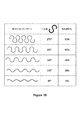
[033]いくつかの実施形態では、例えば、1次単位セル形状は、対向するセグメント、隣接するセグメント、又は対向するセグメントと隣接するセグメントとの組合せなど、複数の空間的にオフセットされた形体を含む。例えば、一実施形態では、1次単位セル形状の空間的にオフセットされた形体は、複数の凸状セグメント、凹状セグメント、円形セグメント、楕円形セグメント、三角形セグメント、長方形セグメント、正方形セグメント、又はこれらの任意の組合せを含む。任意選択で、単位セル形状の凸状セグメント、凹状セグメント、円形セグメント、楕円形セグメント、三角形セグメント、長方形セグメント、又は正方形セグメントは、1つ又は複数の直線セグメントによって分離される。1次単位セルの空間的にオフセットされた形体は、全体的な平面内幾何形状として設けられてもよく、この形体は、基板の支持面に平行な平面内に空間的分散をもたらす。或いは、1次単位セルの空間的にオフセットされた形体は、全体的な平面外幾何形状として設けられてもよく、この形体は、基板の支持面に直交する平面内に空間分散をもたらす。例示的な実施形態では、導電性素子の1次単位セル形状は、コッホ曲線、ペアノ曲線、ヒルベルト曲線、ムーア曲線、Vicsekフラクタル、ギリシャ十字、又はこれらの任意の組合せの1つ又は複数からなる群から選択される。 [033] In some embodiments, for example, the primary unit cell shape comprises a plurality of spatially offset features, such as opposing segments, adjacent segments, or a combination of opposing and adjacent segments. Including. For example, in one embodiment, the spatially offset feature of the primary unit cell shape is a plurality of convex segments, concave segments, circular segments, elliptical segments, triangular segments, rectangular segments, square segments, or Including any combination. Optionally, the unit cell shaped convex, concave, circular, elliptical, triangular, rectangular, or square segments are separated by one or more straight line segments. The spatially offset features of the primary unit cells may be provided as an overall in-plane geometry that provides a spatial dispersion in a plane parallel to the support surface of the substrate. Alternatively, the spatially offset features of the primary unit cells may be provided as an overall out-of-plane geometry that provides spatial dispersion in a plane perpendicular to the support surface of the substrate. In an exemplary embodiment, the primary unit cell shape of the conductive element is a group consisting of one or more of a Koch curve, Peano curve, Hilbert curve, Moore curve, Vicsek fractal, Greek cross, or any combination thereof. Selected from.
[034]特定の実施形態では、例えば、伸縮性金属又は半導体デバイス構成要素は、任意選択で支持面に平行な平面内に設けられる、例えば周期的な、曲がりくねった、分岐状、又はメッシュの幾何形状として設けられる、複数の湾曲形体によって特徴付けられた湾曲構成を有する。特定の実施形態では、例えば、伸縮性金属又は半導体デバイス構成要素は、任意選択で支持面に直交する平面内に設けられる、例えば周期的幾何形状として設けられる、複数の湾曲形体によって特徴付けられた屈曲、座屈、又は皺が寄った構成を有する。 [034] In certain embodiments, for example, the stretchable metal or semiconductor device component is optionally provided in a plane parallel to the support surface, eg, a periodic, tortuous, branched, or mesh geometry. It has a curved configuration characterized by a plurality of curved features provided as a shape. In certain embodiments, for example, the stretchable metal or semiconductor device component is characterized by a plurality of curved features that are optionally provided in a plane orthogonal to the support surface, eg, provided as a periodic geometry. It has a bent, buckled or wrinkled configuration.
[035]特定の実施形態では、例えば、伸縮性金属又は半導体デバイス構成要素が電極又は電極アレイを備える。一実施形態では、電極又は電極アレイは、センサ、アクチュエータ、又は無線周波数デバイスの構成要素である。ある実施形態において、例えば、電極又は電極アレイは、電子回路の作用領域上に、25%〜90%の範囲から選択された充填率をもたらし、任意選択でいくつかの適用例では50%〜90%、任意選択でいくつかの適用例では70%〜90%の充填率をもたらす。 [035] In certain embodiments, for example, a stretchable metal or semiconductor device component comprises an electrode or an electrode array. In one embodiment, the electrode or electrode array is a sensor, actuator, or component of a radio frequency device. In certain embodiments, for example, the electrode or electrode array provides a fill factor selected from a range of 25% to 90% on the active area of the electronic circuit, optionally 50% to 90 in some applications. %, Optionally leading to a filling rate of 70% to 90% in some applications.
[036]本発明のいくつかの電子回路の実施形態の態様は、その他の電子回路及び/又は回路構成要素の間に電気連絡をもたらすのに有用である。例えば、実施形態では、伸縮性金属又は半導体デバイス構成要素が1つ又は複数の電気相互接続を含む。電気相互接続としての、本発明の実施形態の電子回路の使用は、従来の又は剛性の回路構成要素の間の相互接続点として、本発明の実施形態の電子回路の有益な伸縮性態様を与えることにより、従来の又は剛性の回路に伸縮性をもたらす能力を与える。例えばいくつかの実施形態では、電子回路は1つ又は複数の剛性島構造をさらに備え、1つ又は複数の電気相互接続の少なくとも一部分が、1つ又は複数の剛性島構造に電気接触している。一実施形態では、例えば、剛性島構造は無機半導体デバイス又はデバイス構成要素を備える。実施形態では、電子回路は、剛性島構造のそれぞれに電気接触している複数の伸縮性金属又は半導体デバイス構成要素をさらに備える。例えば実施形態では、無機半導体デバイス又はデバイス構成要素は、トランジスタ、ダイオード、増幅器、マルチプレクサ、発光ダイオード、レーザ、光ダイオード、集積回路、センサ、温度センサ、サーミスタ、加熱器、抵抗加熱器、アクチュエータ、又はこれらの任意の組合せを備える。 [036] Some electronic circuit embodiment aspects of the present invention are useful for providing electrical communication between other electronic circuits and / or circuit components. For example, in embodiments, a stretchable metal or semiconductor device component includes one or more electrical interconnects. The use of an electronic circuit of an embodiment of the present invention as an electrical interconnect provides a beneficial stretch aspect of the electronic circuit of an embodiment of the present invention as an interconnection point between conventional or rigid circuit components. This provides the ability to provide elasticity to conventional or rigid circuits. For example, in some embodiments, the electronic circuit further comprises one or more rigid island structures, wherein at least a portion of the one or more electrical interconnects are in electrical contact with the one or more rigid island structures. . In one embodiment, for example, the rigid island structure comprises an inorganic semiconductor device or device component. In embodiments, the electronic circuit further comprises a plurality of stretchable metal or semiconductor device components in electrical contact with each of the rigid island structures. For example, in an embodiment, the inorganic semiconductor device or device component is a transistor, diode, amplifier, multiplexer, light emitting diode, laser, photodiode, integrated circuit, sensor, temperature sensor, thermistor, heater, resistance heater, actuator, or Any combination of these is provided.
[037]様々な弾性基板は、システムの電子回路構成要素に支持及び伸縮性を与えるのに、本発明の実施形態で有用である。ある実施形態では、弾性基板は、0.25μm〜10,000μmの範囲から選択された平均厚さを有し、任意選択でいくつかの適用例では、10μm〜1,000μmの範囲から選択された平均厚さを有する。例えば、一実施形態では、弾性基板は1000μm以下の平均厚さを有する。任意選択で、弾性基板は、予歪状態の弾性基板である。有用な弾性基板は、0.5KPa〜100GPaの範囲から選択されたヤング率、任意選択でいくつかの適用例では10KPa〜100MPaの範囲から選択されたヤング率、任意選択でいくつかの適用例では50KPa〜10MPaの範囲から選択されたヤング率を有するものを含む。有用な弾性基板は、1MPa以下のヤング率、又は0.5MPa以下、又は200KPa以下のヤング率を有するものを含む。有用な弾性基板は、0.1×10⁴GPaμm4〜1×10⁹GPaμm4の範囲から選択された正味の曲げ剛性を有するものを含む。特定の実施形態において、弾性基板は:ポリマー、無機ポリマー、有機ポリマー、プラスチック、エラストマー、バイオポリマー、熱硬化性樹脂、ラバーシルク、及びこれらの任意の組合せからなる群から選択された材料を含む。ある実施形態では、弾性基板は、シリコーンなどの有機シリコン化合物を含む。ある実施形態では、弾性基板はPDMS(ポリジメチルシロキサン)を含む。 [037] Various elastic substrates are useful in embodiments of the present invention to provide support and stretchability to the electronic circuit components of the system. In certain embodiments, the elastic substrate has an average thickness selected from the range of 0.25 μm to 10,000 μm, and optionally selected from the range of 10 μm to 1,000 μm for some applications. Having an average thickness. For example, in one embodiment, the elastic substrate has an average thickness of 1000 μm or less. Optionally, the elastic substrate is a pre-strained elastic substrate. Useful elastic substrates are Young's modulus selected from the range of 0.5 KPa to 100 GPa, optionally in some applications, Young's modulus selected from the range of 10 KPa to 100 MPa, and optionally in some applications. Including those having a Young's modulus selected from the range of 50 KPa to 10 MPa. Useful elastic substrates include those having a Young's modulus of 1 MPa or less, or 0.5 MPa or less, or 200 KPa or less. Useful elastic substrates include those having a net bending stiffness selected from the range of 0.1 × 10 4 GPaμm 4 to 1 × 10 9 GPaμm 4 . In certain embodiments, the elastic substrate comprises a material selected from the group consisting of: a polymer, an inorganic polymer, an organic polymer, a plastic, an elastomer, a biopolymer, a thermosetting resin, rubber silk, and any combination thereof. In some embodiments, the elastic substrate comprises an organosilicon compound such as silicone. In some embodiments, the elastic substrate comprises PDMS (polydimethylsiloxane).
[038]本発明は、光学、電子、熱、機械、及び化学的な感知及び/又は動作を含めた、ある範囲のデバイスの適用例に用いられるシステム及び構成要素を提供する。例えば、様々な実施形態において、この態様の電子回路は、エネルギー貯蔵デバイス、光子デバイス、光センサ、歪みセンサ、電気センサ、温度センサ、化学センサ、アクチュエータ、通信デバイス、ミクロ又はナノ流体デバイス、集積回路、又はこれらの任意の構成要素の1つ又は複数を備える。特定の実施形態では、電子回路は、組織載置型電子デバイス、無線周波数アンテナ、又は磁気共鳴撮像に適合するセンサを備える。 [038] The present invention provides systems and components used in a range of device applications, including optical, electronic, thermal, mechanical, and chemical sensing and / or operation. For example, in various embodiments, an electronic circuit of this aspect includes an energy storage device, a photon device, an optical sensor, a strain sensor, an electrical sensor, a temperature sensor, a chemical sensor, an actuator, a communication device, a micro or nanofluidic device, an integrated circuit Or one or more of these optional components. In certain embodiments, the electronic circuit comprises a tissue-mounted electronic device, a radio frequency antenna, or a sensor that is compatible with magnetic resonance imaging.
[039]本発明の、適切に幾何学的に設計及び/又は構成がなされた回路の実施形態は、従来とは異なる状況、及び/又は電子デバイスが典型的には望ましくない、不適合な、及び/又は動作不能である場合に、本発明の電気回路を使用する能力を与える。例えば、本発明のある実施形態の電子回路は、磁気共鳴撮像に適合する性質を示す。そのような実施形態は、磁気共鳴撮像測定の準備及び/又は実行がなされる間、本発明の電子回路の実施形態とインターフェースをとる組織などの材料の性質の測定及び/又は制御を行う能力を与える。一態様では、例えば、本発明は、磁気共鳴撮像に適合した電子センサを提供する。この態様の特定の実施形態は:弾性基板と;弾性基板によって支持された伸縮性電極アレイとを具備し;電極アレイが、1次単位セル形状をそれぞれが有する複数の導電性素子を備え、導電性素子が、複数の空間周波数によって特徴付けられた全体的な2次元空間幾何形状をもたらす2次形状を有する配列として接続されており;伸縮性電極アレイが、1MHz〜100GHzの範囲から選択された周波数を有する無線周波数電磁放射線を実質的に透過させ(例えば、吸収率が0.1未満、任意選択でいくつかの適用例では0.05未満、さらに任意選択でいくつかの適用例では0.01未満)、伸縮性電極アレイの2次元空間幾何形状が、1つ又は複数の平面内又は平面外の次元に沿って弾性歪みに順応することを可能にし、それによって電子センサの伸縮性がもたらされる。いくつかの実施形態では、例えば伸縮性電極アレイは、電極パッド内に閉ループがないように、電子センサの作用領域上にいかなる閉ループ構造も含まない。ある実施形態では、伸縮性電極アレイは、磁気共鳴撮像と組み合わせて使用するときに、観察可能な歪み又はシャドーイングをもたらさない。実施形態では、例えば磁気共鳴撮像は、100〜300MHzの範囲から選択された周波数を有するRF(無線周波数)パルスへの、電子センサの曝露を含む。 [039] Appropriately geometrically designed and / or configured circuit embodiments of the present invention are different from conventional situations and / or electronic devices are typically undesirable, incompatible, and Provides the ability to use the electrical circuit of the present invention when inoperable. For example, an electronic circuit of an embodiment of the present invention exhibits properties that are compatible with magnetic resonance imaging. Such embodiments provide the ability to measure and / or control the properties of materials such as tissue that interface with embodiments of the electronic circuit of the present invention while magnetic resonance imaging measurements are prepared and / or performed. give. In one aspect, for example, the present invention provides an electronic sensor adapted for magnetic resonance imaging. A particular embodiment of this aspect comprises: an elastic substrate; and a stretchable electrode array supported by the elastic substrate; the electrode array comprising a plurality of conductive elements each having a primary unit cell shape and conducting Are connected as an array having a secondary shape resulting in an overall two-dimensional spatial geometry characterized by multiple spatial frequencies; the stretchable electrode array was selected from the range of 1 MHz to 100 GHz Substantially transmitting radio frequency electromagnetic radiation having a frequency (eg, having an absorptance of less than 0.1, optionally less than 0.05 in some applications, and optionally in some applications less than .0. 01), allowing the two-dimensional spatial geometry of the stretchable electrode array to adapt to elastic strain along one or more in-plane or out-of-plane dimensions, thereby Stretchable child sensor is provided. In some embodiments, for example, the stretchable electrode array does not include any closed loop structure on the active area of the electronic sensor, such that there are no closed loops in the electrode pads. In certain embodiments, the stretchable electrode array does not cause observable distortion or shadowing when used in combination with magnetic resonance imaging. In embodiments, for example, magnetic resonance imaging includes exposure of an electronic sensor to an RF (radio frequency) pulse having a frequency selected from the range of 100-300 MHz.
[040]本発明は、多数の個々にアドレス可能な且つ任意選択で電子的に絶縁された回路構成要素又は電子デバイスなど、アレイ状に設けられた複数の電子デバイス又はデバイス構成要素を備える伸縮性回路を含む。アレイ構成の使用は、実施形態において、サンプル又は組織の表面の個々の異なる領域など、広い領域又は表面とインターフェースをとる能力を持つ本発明の電子回路をもたらす。ある態様では、本発明は、対象又は組織を横断する複数の場所とインターフェースをとるのに有用な電極アレイを提供する。特定の実施形態において、電極アレイは:弾性基板によって支持された複数の伸縮性金属又は半導体デバイス構成要素を具備し、伸縮性金属又は半導体デバイス構成要素のそれぞれが、独立して、1次単位セル形状をそれぞれ有する複数の導電性素子を備え、各伸縮性金属又は半導体デバイス構成要素の導電性素子が、独立して、複数の空間周波数によって特徴付けられた全体的な2次元空間幾何形状をもたらす2次形状を有する配列として接続され;複数の伸縮性金属又は半導体デバイス構成要素が、電極アレイの作用領域に関して50%以上の充填率をもたらし;金属又は半導体デバイス構成要素の2次元空間幾何形状が、1つ又は複数の平面内又は平面外の次元に沿って弾性歪みに順応することを可能にし、それによって電極アレイの伸縮性がもたらされる。 [040] The present invention is a stretch comprising a plurality of electronic devices or device components arranged in an array, such as a number of individually addressable and optionally electronically isolated circuit components or electronic devices. Includes circuitry. The use of an array configuration provides, in embodiments, an electronic circuit of the present invention capable of interfacing with large areas or surfaces, such as individual different areas of the sample or tissue surface. In one aspect, the present invention provides an electrode array useful for interfacing with multiple locations across a subject or tissue. In certain embodiments, the electrode array comprises a plurality of stretchable metal or semiconductor device components supported by an elastic substrate, each of the stretchable metal or semiconductor device components independently being a primary unit cell. A plurality of conductive elements each having a shape, and each conductive metal or semiconductor device component conductive element independently results in an overall two-dimensional spatial geometry characterized by a plurality of spatial frequencies Connected as an array having a secondary shape; multiple stretchable metal or semiconductor device components provide a fill factor of 50% or more with respect to the active area of the electrode array; Allows to adapt to elastic strain along one or more in-plane or out-of-plane dimensions, thereby Compression resistance is brought about.
[041]本発明の実施形態は、本発明の電子回路の実施形態を組み込んだデバイスなどの、伸縮性電子デバイスも提供する。例えば、自己相似幾何形状及び/又は2次元空間周波数を含む電子回路の、より大きい電子デバイスへの組込みは、任意選択で、向上された伸縮性などの有益な特徴を持つ電子デバイスの提供をもたらす。実施形態において、伸縮性デバイスは、剛性及び/又は従来の回路又は回路構成要素と可撓性/伸縮性構成要素を共に、有益な伸縮性態様をデバイスの全体的な構成に与える構成で組み込む。例えば実施形態では、本発明は、本明細書に開示される電子回路及びデバイスを組み込んだ電子デバイスなどの伸縮性電子デバイスを提供する。 [041] Embodiments of the present invention also provide stretchable electronic devices, such as devices incorporating embodiments of the electronic circuit of the present invention. For example, the incorporation of electronic circuits including self-similar geometries and / or two-dimensional spatial frequencies into larger electronic devices optionally results in the provision of electronic devices with beneficial characteristics such as enhanced stretchability. . In embodiments, the stretchable device incorporates both rigid and / or conventional circuitry or circuit components and flexible / stretchable components in a configuration that provides a beneficial stretchability aspect to the overall configuration of the device. For example, in embodiments, the present invention provides stretchable electronic devices, such as electronic devices that incorporate the electronic circuits and devices disclosed herein.
[042]ある態様において、伸縮性電子デバイスは:弾性基板によって支持された複数の剛性島構造と;剛性島構造の少なくとも一部分に電気的に相互接続された複数の伸縮性金属又は半導体デバイス構成要素とを具備し;剛性島構造のそれぞれが、独立して、無機半導体デバイス又はデバイス構成要素を備え、;伸縮性金属又は半導体デバイス構成要素のそれぞれが、独立して、1次単位セル形状をそれぞれが有する複数の導電性素子を備え、各伸縮性金属又は半導体デバイス構成要素の導電性素子が、独立して、複数の空間周波数によって特徴付けられた全体的な2次元空間幾何形状をもたらす2次形状を有する配列として接続され、;金属又は半導体デバイス構成要素の2次元空間幾何形状が、1つ又は複数の平面内又は平面外の次元に沿って弾性歪みに順応することを可能にし、それによって伸縮性電子デバイスの伸縮性がもたらされる。 [042] In certain embodiments, the stretchable electronic device comprises: a plurality of rigid island structures supported by an elastic substrate; and a plurality of stretchable metal or semiconductor device components electrically interconnected to at least a portion of the rigid island structures Each of the rigid island structures independently comprises an inorganic semiconductor device or device component; and each of the stretchable metal or semiconductor device component independently comprises a primary unit cell shape A plurality of conductive elements, wherein each stretchable metal or semiconductor device conductive element independently yields an overall two-dimensional spatial geometry characterized by a plurality of spatial frequencies Connected as an array having a shape; the two-dimensional spatial geometry of a metal or semiconductor device component is along one or more in-plane or out-of-plane dimensions. It makes it possible to adapt the elastic strain Te, thereby providing the elastic stretchable electronic devices.
[043]いかなる特定の理論にも拘泥するものではないが、本明細書に開示されるデバイス及び方法に関する基本原理の信念又は理解に関する考察が、本明細書には見られる。それにも関わらず任意の機械的な説明又は仮説の最終的な正確さとは無関係に、本発明の実施形態は作用的であり且つ有用とすることができることが理解される。 [043] Without being bound to any particular theory, a discussion regarding the belief or understanding of the basic principles relating to the devices and methods disclosed herein can be found herein. Nevertheless, it is understood that embodiments of the present invention can be functional and useful, regardless of the final accuracy of any mechanical explanation or hypothesis.
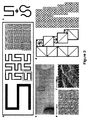
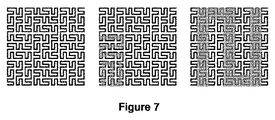
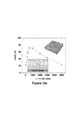
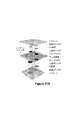
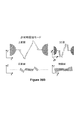
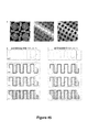
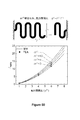
![]()
(a)及び
![]()
(b)対自己相似次数。FEAにおいて、幅は、異なる次数の構造に関してw=0.4l(1)として固定される。
![]()
を有し、厚さ/幅のアスペクト比(t/w=0.03)、及び幅の間隔との比(w/l(1)=0.4)を有するが、これらは異なるフラクタル次数の構造に関するものである。
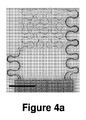
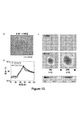
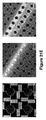
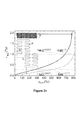
![]()
を有する、1次蛇行相互接続に関する最大主歪み対印加歪み。挿入図は、弾性伸縮性に到達したときの、曲がりくねった相互接続の変形パターンを示す。
![]()
を有する2次フラクタル相互接続に関する最大主歪み対印加歪み:(b)2次構造が完全に解かれたときの、変形していない及び変形した構成を示す図である。
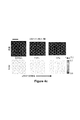
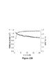
![]()
を有する3次フラクタル相互接続に関する最大主歪み対印加歪み;(b)3次及び2次構造が完全に解かれたときの、変形していない及び変形した構成を示す図である。
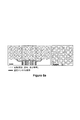
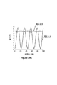
![]()
を有する4次フラクタル相互接続に関する最大主歪み対印加歪み;(b)4次、3次、及び2次構造が完全に解かれたときの、変形していない及び変形した構成を示す図である。
![]()
(A) and
![]()
(B) The degree of self-similarity. In FEA, the width is w = 0.4 l for structures of different orders. (1) As fixed.
![]()
The thickness / width aspect ratio (t / w = 0.03) and the width spacing ratio (w / l (1) = 0.4), but these relate to structures of different fractal orders.
![]()
Maximum principal strain versus applied strain for a primary serpentine interconnect having: The inset shows a twisted interconnect deformation pattern when elastic elasticity is reached.
![]()
(B) Non-deformed and deformed configuration when the secondary structure is fully solved.
![]()
(B) Non-deformed and deformed configuration when the tertiary and secondary structures are fully solved.
![]()
(B) Non-deformed and deformed configuration when the fourth-order, third-order, and second-order structures are fully solved. .
[0111]一般に、本明細書で使用される用語及び文言は、標準的なテキスト、定期刊行物、及び当業者に公知の文脈を参照することによって見出すことができる、それらの技術分野で認識されている意味を有する。下記の定義は、本発明の文脈におけるそれらの特定の使用を明らかにするために提示される。 [0111] In general, the terms and phrases used herein are recognized in the art as can be found by reference to standard texts, periodicals, and contexts known to those skilled in the art. Has a meaning. The following definitions are presented to clarify their specific use in the context of the present invention.
[0112]「2次元空間幾何形状」は、空間における材料、構造、又は構成要素の配置構成であって、それらが、平面を画定する2つの軸などの2つの独立した軸に沿って、又は対象若しくは基板の表面全体に分布している状態を指す。実施形態において、2次元空間幾何形状を保有する対象は、x−y平面内など、2次元のそれぞれの長さに沿って少なくとも一部が横断している材料、構造、又は構成要素を含む。本明細書で使用される「2次元空間幾何形状」は、空間内の2点間を直接延びる材料の線又は薄膜に対応する幾何形状などの、1次元幾何形状とは区別される。実施形態において、2次元空間幾何形状は、表面、例えば平面又は非平面状の表面全体にわたる、共形的な、材料、構造、又は構成要素の配置構成を含む。 [0112] A "two-dimensional spatial geometry" is an arrangement of materials, structures, or components in space, along two independent axes, such as two axes that define a plane, or It refers to the state distributed over the entire surface of the object or substrate. In embodiments, objects possessing a two-dimensional spatial geometry include materials, structures, or components that are at least partially traversed along their respective two-dimensional length, such as in the xy plane. As used herein, a “two-dimensional spatial geometry” is distinguished from a one-dimensional geometric shape, such as a geometric shape corresponding to a line or thin film of material that extends directly between two points in space. In embodiments, the two-dimensional spatial geometry includes conformal material, structure, or component arrangements across a surface, eg, a planar or non-planar surface.
[0113]「複数の空間周波数によって特徴付けられる2次元空間幾何形状」は、空間における材料、構造、又は構成要素の配置構成であって、それらが2つの独立した軸に沿って分布するような、且つ材料、構造、又は構成要素そのものが少なくとも2つの異なる長さスケールにより特徴付けられた周期的若しくは反復している空間構成によって特徴付けられることを指す。実施形態において、複数の空間周波数は、複数の長さスケール、例えば1次単位セル又は短距離長さスケール、2次の、2次形状、又はより長い距離の長さスケール、3次の、3次形状、又は長距離スケールなどによって特徴付けられる。いくつかの実施形態では、2次元空間幾何形状の複数の空間周波数は、フーリエ変換解析など、2次元空間幾何形状に配置構成された材料の空間分布の周波数解析によって特徴付けることができ、材料の空間分布を特徴付ける2つ以上の最大値をもたらす。実施形態において、複数の空間周波数によって特徴付けられた2次元空間幾何形状には、自己相似幾何形状、フラクタル様幾何形状、1〜2の間のフラクタル次元を有する幾何形状であって、任意選択でいくつかの適用例では1.3〜2の間のフラクタル次元を有する幾何形状が含まれるが、これらに限定するものではない。実施形態において、複数の空間周波数によって特徴付けられた2次元空間幾何形状には、ばね内蔵ばね型幾何形状が含まれるが、これに限定するものではない。
[0113] A "two-dimensional spatial geometry characterized by multiple spatial frequencies" is an arrangement of materials, structures, or components in space such that they are distributed along two independent axes And the material, structure, or component itself is characterized by a periodic or repeating spatial composition characterized by at least two different length scales. In embodiments, the plurality of spatial frequencies may include a plurality of length scales, such as a primary unit cell or a short-range length scale, a second-order secondary shape, or a longer-distance length scale, a third-
[0114]「フラクタルベースの2次元幾何形状」は、1つ又は複数の決定的フラクタルパターンをベースにした又はこれらのパターンからその他の手法で誘導された、伸縮性金属又は半導体デバイス構成要素の2次元幾何形状を指す。本発明のフラクタルベースの幾何形状に有用なフラクタルパターンには、ペアノ、Vicsek、ギリシャ十字、及びヒルベルトフラクタルが含まれるが、これらに限定するものではない。フラクタルベースの幾何形状の空間レイアウトは、(1つ又は複数の)レイアウト設計ルールとして、例えば線、周辺、又は形状を使用して(部分的に又は全体的に)、1つ又は複数のフラクタルパターンの形体を組み込む。フラクタルベースの幾何形状は、例えば、フラクタルパターンの鋭い角を、曲がりくねった幾何形状を持つフラクタルパターンのループ又は直線で置き換えることによって、伸縮性及び/又は充填率などの全体的な機械的又はその他の物理的性質を増強するために、任意選択でフラクタルパターンの修正例を組み込んでもよい。実施形態では、本発明で有用なフラクタルベースの幾何形状は、1.2〜2の範囲から選択された近似フラクタル次元によって特徴付けられる。ある実施形態では、本発明で有用なフラクタルベースの幾何形状は、正確な又は近似的な反復ルールによって定義された空間特性を有し、これは、多数の長さスケールによって、より高次のフラクタル様パターンを特徴付けるものである。例えば、N番目の反復パターンが長さスケールL_Nを有し且つN−1番目の反復パターンが長さスケールL_N−1を有する場合、全てのNに関する平均比L_N/L_N−1はAであり、所与のNに関する比L_N/L_N−1はAの±30%以内に包含される。いくつかの実施形態におけるフラクタルベースの幾何形状は、2つ以上の基本的なフラクタル様パターンを線又はメッシュに組み合わせることにより、より大きいフラクタル様パターンを生成する(例えば、図3C参照)。 [0114] "Fractal-based two-dimensional geometry" refers to two of a stretchable metal or semiconductor device component based on or otherwise derived from one or more deterministic fractal patterns. Refers to a dimensional geometry. Fractal patterns useful in the fractal-based geometry of the present invention include, but are not limited to, Peano, Vicsek, Greek cross, and Hilbert fractal. The spatial layout of a fractal-based geometry is one or more fractal patterns (partially or wholly) using, for example, lines, perimeters or shapes as layout design rule (s). Incorporate the form of Fractal-based geometries can be used for example to replace the sharp corners of a fractal pattern with loops or straight lines of a fractal pattern with a tortuous geometry, such as overall mechanical or other such as stretchability and / or filling factor. In order to enhance physical properties, a fractal pattern modification may optionally be incorporated. In embodiments, the fractal based geometry useful in the present invention is characterized by an approximate fractal dimension selected from the range of 1.2-2. In certain embodiments, the fractal-based geometry useful in the present invention has spatial characteristics defined by exact or approximate iterative rules, which can be achieved by higher length fractals with multiple length scales. It characterizes the pattern. For example, if the Nth repeating pattern has a length scale L_N and the N−1th repeating pattern has a length scale L_N−1, the average ratio L_N / L_N−1 for all N is A; The ratio L_N / L_N−1 for a given N is included within ± 30% of A. The fractal-based geometry in some embodiments generates a larger fractal-like pattern by combining two or more basic fractal-like patterns into a line or mesh (see, eg, FIG. 3C).
[0115]「充填率」は、材料、要素、及び/又はデバイス構成要素の支持及び/又はこれらの要素による占有がなされる、第1及び第2の電気接触点、デバイス島、又は接触パッドなどの2つの要素間の面積のパーセンテージを指す。ある実施形態では例えば、充填率は、1つ又は複数の伸縮性金属又は半導体デバイス構成要素を支持する(及び任意選択で、物理接触する)弾性基板の表面又はその上に設けられた層の表面などの、表面の領域のパーセンテージを指す。ある実施形態では例えば、充填率は、1つ又は複数の伸縮性金属又は半導体デバイス構成要素を支持する(任意選択で物理接触する)、デバイスの作用領域上の領域のパーセンテージを指す。ある実施形態では例えば、充填率は、1つ又は複数の伸縮性金属又は半導体デバイス構成要素を支持する(任意選択で物理接触する)、半導体デバイス構成要素又はデバイスなどの2つのデバイス島の間に拡がる表面のパーセンテージを指す。ある実施形態では例えば、充填率は、1つ又は複数の伸縮性金属又は半導体デバイス構成要素を支持する、第1及び第2の電気接触点又は接触パッドなどの2つの要素間に拡がる表面部分の面積のパーセンテージを指す。 [0115] "Filling rate" refers to first and second electrical contact points, device islands, contact pads, etc. that are supported and / or occupied by materials, elements, and / or device components. The percentage of the area between the two elements. In some embodiments, for example, the fill factor is the surface of an elastic substrate that supports (and optionally physically contacts) one or more stretchable metal or semiconductor device components, or the surface of a layer disposed thereon Refers to the percentage of the surface area. In some embodiments, for example, the fill factor refers to the percentage of the area on the active area of the device that supports (optionally in physical contact) one or more stretchable metal or semiconductor device components. In certain embodiments, for example, the fill factor is between two device islands, such as a semiconductor device component or device, that supports (optionally in physical contact) one or more stretchable metal or semiconductor device components. Refers to the percentage of the surface that spreads. In one embodiment, for example, the fill factor is a surface portion that extends between two elements, such as first and second electrical contact points or contact pads, that support one or more stretchable metal or semiconductor device components. Refers to the area percentage.
[0116]「機能層」は、デバイスにいくらかの機能性を与える層を指す。例えば機能層は、半導体構成要素を含有していてもよい。或いは機能層は、支持層によって分離された多数の半導体層など、多数の層を含んでいてもよい。機能層は、電極又は島の間又はそれらの下を走る相互接続など、複数のパターニングされた要素を備えていてもよい。機能層は、均質であってもよく、又は不均質な1つ若しくは複数の性質若しくは材料を有していてもよい。「不均質な性質」は、空間的に変化し得る物理的パラメータを指し、それによって、多層デバイス内の中立機械平面の位置を有効にする。 [0116] "Functional layer" refers to a layer that imparts some functionality to the device. For example, the functional layer may contain a semiconductor component. Alternatively, the functional layer may include multiple layers, such as multiple semiconductor layers separated by a support layer. The functional layer may comprise a plurality of patterned elements, such as interconnects that run between or under the electrodes or islands. The functional layer may be homogeneous or may have one or more properties or materials that are heterogeneous. “Inhomogeneous nature” refers to a physical parameter that can vary spatially, thereby enabling the position of the neutral mechanical plane within the multilayer device.
[0117]「構造層」は、例えばデバイス構成要素の支持及び/又は包封及び/又は分割を行うことによって構造的機能性を与える層を指す。 [0117] "Structural layer" refers to a layer that provides structural functionality, for example, by supporting and / or encapsulating and / or dividing device components.
[0118]「半導体」は、非常に低い温度で絶縁体であるが、約300ケルビンの温度で明らかな導電性を有する任意の材料を指す。本発明の記述において、半導体という用語の使用は、マイクロエレクトロニクス及び電子デバイスの分野でのこの用語の使用と矛盾しないものとする。有用な半導体には、シリコン、ゲルマニウム、及びダイヤモンドなどの元素半導体と、化合物半導体、例えば、SiC及びSiGeなどのIV族化合物半導体、AlSb、AlAs、AlN、AlP、BN、BP、BAs、GaSb、GaAs、GaN、GaP、InSb、InAs、InN、及びInPなどのIII−V族半導体、AlxGa1−xAsなどのIII−V族3元半導体、CsSe、CdS、CdTe、ZnO、ZnSe、ZnS、及びZnTeなどのII−VI族半導体、CuClなどのI−VII族半導体、PbS、PbTe、及びSnSなどのIV−VI族半導体、PbI2、MoS2、及びGaSeなどの層半導体、CuO及びCu2Oなどの酸化物半導体を含むものが含まれる。半導体という用語は、真性半導体、及び1種又は複数の選択された材料がドープされた不純物半導体を含み、所与の適用例又はデバイスに有用な有益な電子特性を得るためにp型ドーピング材料及びn型ドーピング材料を有する半導体が含まれる。半導体という用語は、半導体及び/又はドーパントの混合物を含んだ複合材料を含む。いくつかの実施形態に有用な特定の半導体材料には、Si、Ge、Se、ダイヤモンド、フラーレン、SiC、SiGe、SiO、SiO2、SiN、AlSb、AlAs、AlIn、AlN、AlP、AlS、BN、BP、BAs、As2S3、GaSb、GaAs、GaN、GaP、GaSe、InSb、InAs、InN、InP、CsSe、CdS、CdSe、CdTe、Cd3P2、Cd3As2、Cd3Sb2、ZnO、ZnSe、ZnS、ZnTe、Zn3P2、Zn3As2、Zn3Sb2、ZnSiP2、CuCl、PbS、PbSe、PbTe、FeO、FeS2、NiO、EuO、EuS、PtSi、TlBr、CrBr3、SnS、SnTe、PbI2、MoS2、GaSe、CuO、Cu2O、HgS、HgSe、HgTe、HgI2、MgS、MgSe、MgTe、CaS、CaSe、SrS、SrTe、BaS、BaSe、BaTe、SnO2、TiO、TiO2、Bi2S3、Bi2O3、Bi2Te3、BiI3、UO2、UO3、AgGaS2、PbMnTe、BaTiO3、SrTiO3、LiNbO3、La2CuO4、La0.7Ca0.3MnO3、CdZnTe、CdMnTe、CuInSe2、銅インジウムガリウムセレン化物(CIGS)、HgCdTe、HgZnTe、HgZnSe、PbSnTe、Tl2SnTe5、Tl2GeTe5、AlGaAs、AlGaN、AlGaP、AlInAs、AlInSb、AlInP、AlInAsP、AlGaAsN、GaAsP、GaAsN、GaMnAs、GaAsSbN、GaInAs、GaInP、AlGaAsSb、AlGaAsP、AlGaInP、GaInAsP、InGaAs、InGaP、InGaN、InAsSb、InGaSb、InMnAs、InGaAsP、InGaAsN、InAlAsN、GaInNAsSb、GaInAsSbP、及びこれらの任意の組合せが含まれるが、これらに限定するものではない。多孔質シリコン半導体材料は、本明細書に記述される態様に有用である。半導体材料の不純物は、(1種又は複数の)半導体材料そのもの以外の原子、元素、イオン、及び/又は分子であり、又は、半導体材料に提供される任意のドーパントである。不純物は、半導体材料の電子特性に悪影響を及ぼし得る、半導体材料中に存在する望ましくない材料であり、酸素、炭素、及び重金属を含めた金属が含まれるがこれらに限定するものではない。重金属不純物には、周期表上の銅から鉛までの元素の群、カルシウム、ナトリウム、及び全てのイオン、化合物、及び/又はそれらの錯体が含まれるが、これらに限定するものではない。 [0118] "Semiconductor" refers to any material that is an insulator at a very low temperature but has a clear conductivity at a temperature of about 300 Kelvin. In the description of the invention, the use of the term semiconductor shall be consistent with the use of this term in the field of microelectronics and electronic devices. Useful semiconductors include elemental semiconductors such as silicon, germanium, and diamond, and compound semiconductors such as group IV compound semiconductors such as SiC and SiGe, AlSb, AlAs, AlN, AlP, BN, BP, BAs, GaSb, GaAs , GaN, GaP, InSb, InAs, InN, and InP group III-V semiconductors, III x V group ternary semiconductors such as Al x Ga 1-x As, CsSe, CdS, CdTe, ZnO, ZnSe, ZnS, and group II-VI semiconductors such as ZnTe, I-VII semiconductors such as CuCl, PbS, PbTe, and group IV-VI semiconductors such as SnS, PbI 2, MoS 2, and the layer semiconductors such as GaSe, CuO and Cu 2 Those containing an oxide semiconductor such as O are included. The term semiconductor includes intrinsic semiconductors, and impurity semiconductors doped with one or more selected materials, p-type doping materials to obtain useful electronic properties useful for a given application or device, and A semiconductor having an n-type doping material is included. The term semiconductor includes composite materials comprising a mixture of semiconductors and / or dopants. Some implementations particular semiconductor materials useful in the form, Si, Ge, Se, diamond, fullerene, SiC, SiGe, SiO, SiO 2, SiN, AlSb, AlAs, AlIn, AlN, AlP, AlS, BN, BP, BAs, As 2 S 3 , GaSb, GaAs, GaN, GaP, GaSe, InSb, InAs, InN, InP, CsSe, CdS, CdSe, CdTe, Cd 3 P 2 , Cd 3 As 2 , Cd 3 Sb 2 ZnO, ZnSe, ZnS, ZnTe, Zn 3 P 2, Zn 3 As 2, Zn 3 Sb 2, ZnSiP 2, CuCl, PbS, PbSe, PbTe, FeO, FeS 2, NiO, EuO, EuS, PtSi, TlBr, CrBr 3 , SnS, SnTe, PbI 2 , MoS 2 , GaSe, CuO, Cu 2 O, HgS, HgSe, HgTe, HgI 2 , MgS, MgSe, MgTe, CaS, CaSe, SrS, SrTe, BaS, BaSe, BaTe, SnO 2 , TiO, TiO 2 , Bi 2 S 3 , Bi 2 O 3 , Bi 2 Te 3 , BiI 3 , UO 2 , UO 3 , AgGaS 2 , PbMnTe, BaTiO 3 , SrTiO 3 , LiNbO 3 , La 2 CuO 4 , La 0.7 Ca 0.3 MnO 3 , CdMnTe, CdMnTe 2, copper indium gallium selenide (CIGS), HgCdTe, HgZnTe, HgZnSe, PbSnTe, Tl 2 SnTe 5, Tl 2 GeTe 5, AlGaAs, AlGaN, AlGaP, AlInAs, AlInSb, AlInP, AlInAsP, AlGa sN, GaAsP, GaAsN, GaMnAs, GaAsSbN, GaInAs, GaInP, AlGaAsSb, AlGaAsP, AlGaInP, GaInAsP, InGaAs, InGaP, InGaN, InAsSb, InGaSb, InMnAs, InGaAsP, InGaAsN, InAlAsSb, InAlAsSb, InAsAsSb, InAsAsSb However, it is not limited to these. Porous silicon semiconductor materials are useful for the embodiments described herein. The impurities of the semiconductor material are atoms, elements, ions, and / or molecules other than the semiconductor material (s) itself, or any dopant provided to the semiconductor material. Impurities are undesirable materials present in a semiconductor material that can adversely affect the electronic properties of the semiconductor material and include, but are not limited to, metals including oxygen, carbon, and heavy metals. Heavy metal impurities include, but are not limited to, a group of elements from copper to lead on the periodic table, calcium, sodium, and all ions, compounds, and / or complexes thereof.
[0119]「半導体構成要素」は、任意の半導体材料、組成物、又は構造を広く指し、高品質単結晶及び多結晶半導体、高温加工を介して製作された半導体材料、ドープ型半導体材料、無機半導体、及び複合半導体材料を明らかに含む。いくつかの実施形態では、例えば、半導体構成要素が半導体デバイス又はその構成要素である。 [0119] "Semiconductor component" broadly refers to any semiconductor material, composition, or structure, high quality single crystal and polycrystalline semiconductors, semiconductor materials fabricated through high temperature processing, doped semiconductor materials, inorganic It clearly includes semiconductors and composite semiconductor materials. In some embodiments, for example, the semiconductor component is a semiconductor device or a component thereof.
[0120]「構成要素」は、デバイスの個々の部分を指すのに広く使用される。「相互接続」は、構成要素の一例であり、別の構成要素と又は構成要素間で電気接続を確立することが可能な導電性構造を指す。特に、相互接続は、個別の構成要素間に電気接触を確立してもよい。所望のデバイスの仕様、動作、及び適用例に応じて、相互接続は適切な材料から作製される。適切な導電性材料には半導体が含まれる。いくつかの実施形態では、例えば、構成要素が半導体デバイスの構成要素である。 [0120] "Component" is used broadly to refer to individual parts of a device. “Interconnect” is an example of a component and refers to a conductive structure capable of establishing an electrical connection with another component or between components. In particular, an interconnect may establish electrical contact between individual components. Depending on the desired device specification, operation, and application, the interconnect is made from a suitable material. Suitable conductive materials include semiconductors. In some embodiments, for example, the component is a component of a semiconductor device.
[0121]その他の構成要素には、薄膜トランジスタ(TFT)、トランジスタ、電極、集積回路、回路素子、制御素子、マイクロプロセッサ、トランスデューサ、島、ブリッジ、及びこれらの組合せが含まれるが、これらに限定するものではない。構成要素は、例えば金属蒸着、ワイヤボンディング、及び固形分又は導電性ペーストの付着などにより、当技術分野で公知の1つ又は複数の接触パッドに接続されてもよい。 [0121] Other components include, but are not limited to, thin film transistors (TFTs), transistors, electrodes, integrated circuits, circuit elements, control elements, microprocessors, transducers, islands, bridges, and combinations thereof. It is not a thing. The component may be connected to one or more contact pads known in the art, for example, by metal deposition, wire bonding, and solid or conductive paste deposition.
[0122]「中立機械平面」(NMP)は、デバイスの横b及び縦lの方向に存在する仮想平面を指す。NMPは、デバイスの垂直h軸に沿ったさらに極端な位置に在るデバイスのその他の平面及び/又はデバイスのより屈曲性ある層の内部よりも、屈曲応力をそれほど受けない。このように、NMPの位置は、デバイスの厚さ及びデバイスの(1つ又は複数の)層を形成する材料の両方によって決定される。 [0122] A "neutral machine plane" (NMP) refers to a virtual plane that exists in the direction of the horizontal b and vertical l of the device. NMP is less subject to bending stresses than other planes of the device and / or the interior of a more flexible layer of the device at more extreme locations along the vertical h-axis of the device. Thus, the location of the NMP is determined by both the thickness of the device and the material that forms the layer (s) of the device.
[0123]「同時発生」は、2つ以上の対象、平面、又は表面の相対位置、例えば、機能層、基板層、又はその他の層などの、層の内部又は層に隣接して位置決めされた中立機械平面の表面の相対位置を指す。ある実施形態では、中立機械平面は、層内の最も歪みを感受する層又は材料に対応するように位置決めされる。 [0123] "Co-occurrence" is positioned in or adjacent to a relative position of two or more objects, planes, or surfaces, eg, functional layer, substrate layer, or other layer Refers to the relative position of the neutral machine plane surface. In certain embodiments, the neutral machine plane is positioned to correspond to the most strain sensitive layer or material in the layer.
[0124]「近接」は、2つ以上の対象、平面、又は表面の相対位置、例えば、歪み感受性材料の物理的性質に悪影響を及ぼすことなく所望の順応性を提供しながら、機能層、基板層、又はその他の層などの層の位置に密接に従う中立機械平面の相対位置を指す。「歪み感受性」は、比較的低レベルの歪みに応答して破砕され又はその他の理由で損なわれる材料を指す。一般に、高い歪み感受性を有し且つ結果として第1の層を破砕させ易くする層は、機能層、例えば比較的脆弱な半導体又はその他の歪み感受性デバイス素子を含有する機能層内に位置付けられる。層に近接する中立機械平面は、その層の内部に拘束される必要がなく、歪み感受性デバイス素子に対する歪みを低減させる機能的な利益が得られるように、近接して又は十分近くに位置決めされてもよい。 [0124] "Proximity" refers to a functional layer, a substrate, while providing the desired flexibility without adversely affecting the relative position of two or more objects, planes, or surfaces, eg, the physical properties of strain sensitive materials. Refers to the relative position of a neutral machine plane that closely follows the position of a layer, such as a layer or other layer. “Strain sensitivity” refers to a material that is crushed or otherwise damaged in response to relatively low levels of strain. In general, a layer that has a high strain sensitivity and consequently facilitates the fracture of the first layer is located in a functional layer, such as a functional layer containing a relatively fragile semiconductor or other strain sensitive device element. The neutral mechanical plane adjacent to the layer does not need to be constrained within the layer and is positioned close enough or close enough to provide a functional benefit to reduce strain on the strain sensitive device elements. Also good.
[0125]「一体」は、単片又は分割されていない全体として形成された対象を指す。 [0125] "Integral" refers to an object formed as a single piece or as a whole that is not divided.
[0126]「直接及び間接」という用語は、別の構成要素に対する1つの構成要素の、又は別のデバイスに対する1つのデバイスの、動作又は物理的位置について記述する。例えば、別の構成要素に「直接」作用し又は接触する構成要素は、仲介物からの介入なしでそのように作用し接触する。逆に、別の構成要素に「間接的」に作用し又は接触する構成要素は、仲介物(例えば、第3の構成要素)を通してそのように作用し接触する。 [0126] The term "direct and indirect" describes the operation or physical location of one component relative to another component, or one device relative to another device. For example, a component that acts or contacts “directly” with another component acts and contacts that way without intervention from an intermediary. Conversely, a component that acts or contacts "indirectly" with another component acts and contacts that way through an intermediary (eg, a third component).
[0127]「電子デバイス」は、一般に、複数の構成要素を組み込むデバイスを指し、大面積エレクトロニクス、プリントワイヤ基板、集積回路、コンポーネントアレイ、電気生理学及び/又は生物学及び/又は化学センサ、及び物理センサ(例えば、温度、加速度など)を含む。 [0127] "Electronic device" generally refers to a device that incorporates multiple components, such as large area electronics, printed wire boards, integrated circuits, component arrays, electrophysiology and / or biological and / or chemical sensors, and physics Includes sensors (eg, temperature, acceleration, etc.).
[0128]「感知」は、物理的及び/又は化学的性質の存在、不在、量、大きさ、又は強度を検出することを指す。感知するための有用な電子デバイス構成要素には、電極素子、化学又は生物センサ素子、pHセンサ、加速度計、温度センサ、及び容量センサが含まれるが、これらに限定するものではない。 [0128] "Sensing" refers to detecting the presence, absence, amount, magnitude, or intensity of a physical and / or chemical property. Useful electronic device components for sensing include, but are not limited to, electrode elements, chemical or biological sensor elements, pH sensors, accelerometers, temperature sensors, and capacitive sensors.
[0129]「島」は、複数の半導体構成要素を備える電子デバイスの、比較的剛性の構成要素を指す。「ブリッジ」は、2つ以上の島又は1つの島を別の構成要素に相互接続する構造を指す。本発明は、電気接触と半導体デバイス構成要素との間及び内部に設けられた伸縮性電気相互接続など、電気相互接続を含んだブリッジ構造を有する電子デバイスを含む。 [0129] "Island" refers to a relatively rigid component of an electronic device comprising a plurality of semiconductor components. “Bridge” refers to a structure that interconnects two or more islands or one island to another component. The present invention includes an electronic device having a bridge structure including electrical interconnects, such as stretchable electrical interconnects provided between and within electrical contacts and semiconductor device components.
[0130]「包封」は、少なくとも部分的に及びある場合には完全に、1つ又は複数のその他の構造によって取り囲まれるような、1つの構造の配向を指す。「部分的に包封された」は、1つ又は複数のその他の構造によって部分的に取り囲まれるような、1つの構造の配向であって、例えば、構造の外面の30%又は任意選択で50%又は任意選択で90%が1つ又は複数の構造によって取り囲まれるような配向を指す。「完全に包封された」は、1つ又は複数のその他の構造によって完全に取り囲まれるような、1つの構造の配向を指す。 [0130] "Encapsulation" refers to an orientation of a structure such that it is at least partially and in some cases completely surrounded by one or more other structures. “Partially encapsulated” is an orientation of one structure that is partially surrounded by one or more other structures, for example, 30% of the outer surface of the structure or optionally 50 % Or optionally 90% refers to an orientation such that it is surrounded by one or more structures. “Completely encapsulated” refers to an orientation of one structure such that it is completely surrounded by one or more other structures.
[0131]「隣接する」は、破壊されていない配列全体を通して接触し又は接続されている材料又は層を指す。一実施形態において、デバイスの隣接層は、当初から設けられている材料又は層のかなりの部分(例えば、10%以上)を除去するように処理されていない。 [0131] "Adjacent" refers to a material or layer that is in contact or connected throughout an unbroken array. In one embodiment, adjacent layers of the device are not treated to remove a significant portion (eg, 10% or more) of the originally provided material or layer.
[0132]「能動回路」及び「能動回路構成」は、特定の機能を発揮させるために構成された1つ又は複数の構成要素を指す。有用な能動回路には、増幅器回路、多重化回路、電流制限回路、集積回路、インピーダンス整合回路、ワイヤレス電力収穫回路、ワイヤレスデータ伝送回路、トランジスタ、及びトランジスタアレイが含まれるが、これらに限定するものではない。 [0132] "Active circuit" and "active circuit configuration" refer to one or more components configured to perform a particular function. Useful active circuits include, but are not limited to, amplifier circuits, multiplexing circuits, current limiting circuits, integrated circuits, impedance matching circuits, wireless power harvesting circuits, wireless data transmission circuits, transistors, and transistor arrays. is not.
[0133]「基板」は、1つ又は複数の構成要素又は電子デバイスを支持することが可能な受容面又は支持面などの表面を有する、材料、層、又はその他の構造を指す。基板に「結合された」構成要素は、基板に物理接触しており且つこの構成要素が結合している基板表面に対して実質的に移動させることができない構成要素を指す。対照的に、結合していない構成要素又は構成要素の部分は、基板に対して実質的な移動が可能になる。ある実施形態では、本発明は、基板によって支持された、任意選択で基板に物理接触しており又は基板により支持された1つ又は複数の中間体構造に物理接触している、1つ又は複数の自立半導体デバイス構成要素を有する電子デバイスを含む。ある実施形態では、本発明は、半導体デバイス構成要素を基板に独立して接続させる、ペデスタル又はペデスタルのアレイなどの1つ又は複数の構造によって支持された又は任意選択で結合された、1つ又は複数の繋留半導体デバイス構成要素を有する電子デバイスを含む。 [0133] "Substrate" refers to a material, layer, or other structure having a surface, such as a receiving surface or support surface, that can support one or more components or electronic devices. A component “coupled” to a substrate refers to a component that is in physical contact with the substrate and cannot be moved substantially relative to the substrate surface to which the component is bonded. In contrast, an uncoupled component or component part is allowed to move substantially relative to the substrate. In certain embodiments, the present invention includes one or more physical supports in one or more intermediate structures supported by a substrate, optionally in physical contact with or supported by the substrate. An electronic device having a self-supporting semiconductor device component. In certain embodiments, the present invention supports one or more structures supported or optionally coupled by one or more structures, such as pedestals or arrays of pedestals, that independently connect semiconductor device components to a substrate. An electronic device having a plurality of tethered semiconductor device components is included.
[0134]「自立」は、デバイス又はデバイス構成要素が、基板によって、又はデバイス若しくはデバイス構成要素と基板との間に設けられた中間体構造によって、支持されているが結合されていない構成を指す。ある実施形態では、例えば、基板を、この基板により支持された自立デバイス又は構成要素に対して移動させることができる。ある実施形態では、例えば、自立デバイス又は構成要素は、自立デバイス又は構成要素を支持する基板に対して移動させることができる。いくつかの実施形態では、例えば、デバイス又はデバイス構成要素の自立構成は、基板の動き及び/又は変形をデバイス又はデバイス構成要素から切り離す。いくつかの実施形態では、例えば、デバイス又はデバイス構成要素の自立構成が、基板の伸び、圧縮、又は変形によって発生した力を、デバイス又はデバイス構成要素から切り離す。いくつかの実施形態では、自立デバイス又は構成要素は、ファンデルワールツ相互作用、双極子間相互作用、又はその他の非共有結合性相互作用など、基板表面又はその上に設けられた中間体構造との、結合性相互作用を受けることによって特徴付けられる。ある実施形態では、自立デバイス又は構成要素は、基板の支持表面に共有結合されていない。 [0134] "Free-standing" refers to a configuration in which a device or device component is supported but not bonded by a substrate or by an intermediate structure provided between the device or device component and the substrate. . In some embodiments, for example, the substrate can be moved relative to a freestanding device or component supported by the substrate. In certain embodiments, for example, a free standing device or component can be moved relative to a substrate that supports the free standing device or component. In some embodiments, for example, a self-supporting configuration of the device or device component decouples substrate movement and / or deformation from the device or device component. In some embodiments, for example, a self-supporting configuration of the device or device component decouples the force generated by stretching, compression, or deformation of the substrate from the device or device component. In some embodiments, the freestanding device or component is a substrate surface or intermediate structure provided thereon, such as van der Waals interactions, dipole-to-dipole interactions, or other non-covalent interactions. Characterized by undergoing binding interactions. In certain embodiments, the freestanding device or component is not covalently bonded to the support surface of the substrate.
[0135]「繋留」は、デバイス又は構成要素が、ペデスタル又はペデスタルのアレイなどの1つ又は複数の繋留構造を介して、基板に接続された構成を指す。ある実施形態では、例えば、基板は、基板によって支持された繋留デバイス又は構成要素に対して移動することができる。ある実施形態では、例えば、繋留デバイス又は構成要素は、繋留デバイス又は構成要素を支持する基板に対して移動することができる。いくつかの実施形態では、例えば、デバイス又はデバイス構成要素の繋留構成が、基板の動き及び/又は変形をデバイス又はデバイス構成要素から切り離す。いくつかの実施形態では、例えば、デバイス又はデバイス構成要素の繋留構成が、基板の伸び、圧縮、又は変形により発生した力を、デバイス又はデバイス構成要素から切り離す。いくつかの実施形態では、デバイス又は構成要素の底面の面積の20%未満、任意選択で5%未満、及び任意選択で1%未満が、基板に結合された繋留構造に共有結合される。 [0135] "Tethered" refers to a configuration in which a device or component is connected to a substrate via one or more tethered structures such as a pedestal or an array of pedestals. In certain embodiments, for example, the substrate can move relative to a tethering device or component supported by the substrate. In certain embodiments, for example, the anchoring device or component can be moved relative to the substrate that supports the anchoring device or component. In some embodiments, for example, a tethered configuration of a device or device component decouples substrate movement and / or deformation from the device or device component. In some embodiments, for example, the tethered configuration of the device or device component decouples the force generated by stretching, compressing, or deforming the substrate from the device or device component. In some embodiments, less than 20%, optionally less than 5%, and optionally less than 1% of the area of the bottom surface of the device or component is covalently bonded to the anchoring structure bonded to the substrate.
[0136]「ナノ構造化表面」及び「ミクロ構造化表面」は、それぞれナノメートルサイズ及びマイクロメートルサイズのレリーフ形体を有するデバイス表面を指す。レリーフ形体は、デバイス表面の実質的に隣接する平面から長さxを伸びる。構造化表面の定量的記述子は、原子間力顕微鏡法(AFM)によってその全てが測定され得るRmax、Ra、及び正規化粗さ(Ra/Rmax)などの表面粗さパラメータを含む。Rmaxは、最高ピークと最低バレーとの間の最大高さである。Raは、粗さ曲線から粗さ曲線までの中心線からの偏差の絶対値の平均である、中心線平均粗さである。基板又は層の表面は、本開示の目的で表面が100nm以下のRa値を有する場合に「実質的に滑らか」である。表面が、100nmよりも大きいRa値を有する場合、表面は、本開示の目的で「構造化表面」と見なされる。 [0136] "Nanostructured surface" and "microstructured surface" refer to device surfaces having nanometer-sized and micrometer-sized relief features, respectively. The relief feature extends a length x from a substantially adjacent plane of the device surface. Quantitative descriptors for structured surfaces include surface roughness parameters such as R max , R a , and normalized roughness (R a / R max ), all of which can be measured by atomic force microscopy (AFM). Including. R max is the maximum height between the highest peak and the lowest valley. R a is the average of the absolute value of the deviation from the center line of the roughness curve to the roughness curve, the center line average roughness. The surface of the substrate or layer is “substantially smooth” when the surface has an Ra value of 100 nm or less for purposes of this disclosure. A surface is considered a “structured surface” for purposes of this disclosure if the surface has an Ra value greater than 100 nm.
[0137]「誘電体」は、非導電性又は絶縁性材料を指す。実施形態において、無機誘電体は、実質的に炭素を含まない誘電体材料を含む。無機誘電体材料の特定の例には、窒化ケイ素、二酸化ケイ素、及び非共役ポリマーが含まれるが、これらに限定するものではない。 [0137] "Dielectric" refers to a non-conductive or insulating material. In an embodiment, the inorganic dielectric includes a dielectric material that is substantially free of carbon. Specific examples of inorganic dielectric materials include, but are not limited to, silicon nitride, silicon dioxide, and non-conjugated polymers.
[0138]「ポリマー」は、共有化学結合によって接続された繰返し構造単位から構成された高分子、又は高分子量によってしばしば特徴付けられる1つ若しくは複数のモノマーの重合生成物を指す。ポリマーという用語は、ホモポリマー、又は単一繰返しモノマーサブ単位から本質的になるポリマーを含む。ポリマーという用語は、コポリマー、又は2つ以上のモノマーサブ単位から本質的になるポリマー、例えばランダム、ブロック、交互、セグメント化、グラフト、テーパー、及びその他のコポリマーも含む。有用なポリマーには、非晶質、半非晶質、結晶質、又は部分結晶質状態にあってもよい有機ポリマー又は無機ポリマーが含まれる。連結されたモノマー鎖を有する架橋ポリマーは、いくつかの適用例で特に有用である。方法、デバイス、及び構成要素で使用可能なポリマーには、プラスチック、エラストマー、熱可塑性エラストマー、弾性プラスチック、熱可塑性樹脂、及びアクリレートが含まれるが、これらに限定するものではない。例示的なポリマーには、アセタールポリマー、生分解性ポリマー、セルロースポリマー、フルオロポリマー、ナイロン、ポリアクリロニトリルポリマー、ポリアミド−イミドポリマー、ポリイミド、ポリアリーレート、ポリベンズイミダゾール、ポリブチレン、ポリカーボネート、ポリエステル、ポリエーテルイミド、ポリエチレン、ポリエチレンコポリマー及び修飾ポリエチレン、ポリケトン、ポリ(メチルメタクリレート)、ポリメチルペンテン、ポリフェニレンオキシド及びポリフェニレンスルフィド、ポリフタルアミド、ポリプロピレン、ポリウレタン、スチレン系樹脂、スルホン系樹脂、ビニル系樹脂、ゴム(天然ゴム、スチレン−ブタジエン、ポリブタジエン、ネオプレン、エチレン−プロピレン、ブチル、ニトリル、シリコーンを含む。)、アクリル、ナイロン、ポリカーボネート、ポリエステル、ポリエチレン、ポリプロピレン、ポリスチレン、ポリ塩化ビニル、ポリオレフィン、又はこれらの任意の組合せが含まれるが、これらに限定するものではない。 [0138] "Polymer" refers to a polymer composed of repeating structural units connected by covalent chemical bonds, or the polymerization product of one or more monomers often characterized by high molecular weight. The term polymer includes homopolymers or polymers consisting essentially of a single repeating monomer subunit. The term polymer also includes copolymers, or polymers consisting essentially of two or more monomeric subunits, such as random, block, alternating, segmented, grafted, tapered, and other copolymers. Useful polymers include organic or inorganic polymers that may be in an amorphous, semi-amorphous, crystalline, or partially crystalline state. Crosslinked polymers having linked monomer chains are particularly useful in some applications. Polymers that can be used in the methods, devices, and components include, but are not limited to, plastics, elastomers, thermoplastic elastomers, elastic plastics, thermoplastics, and acrylates. Exemplary polymers include acetal polymers, biodegradable polymers, cellulose polymers, fluoropolymers, nylons, polyacrylonitrile polymers, polyamide-imide polymers, polyimides, polyarylates, polybenzimidazoles, polybutylenes, polycarbonates, polyesters, polyethers. Imido, polyethylene, polyethylene copolymer and modified polyethylene, polyketone, poly (methyl methacrylate), polymethylpentene, polyphenylene oxide and polyphenylene sulfide, polyphthalamide, polypropylene, polyurethane, styrene resin, sulfone resin, vinyl resin, rubber ( Natural rubber, styrene-butadiene, polybutadiene, neoprene, ethylene-propylene, butyl, nitrile, silicon Including.), Acrylic, nylon, polycarbonate, polyester, polyethylene, polypropylene, polystyrene, polyvinyl chloride, polyolefin, or any combination thereof, not limited thereto.
[0139]「エラストマースタンプ」及び「エラストマー転移デバイス」は、同義に使用され、材料を受容すると共に転移させることができる表面を有するエラストマー材料を指す。例示的なエラストマー転移デバイスには、スタンプ、モールド、及びマスクが含まれる。転移デバイスは、供与体材料から受容体材料への材料の転移に対する影響及び/又は促進をもたらす。 [0139] "Elastomer stamp" and "elastomeric transfer device" are used interchangeably and refer to an elastomeric material having a surface that can receive and transfer material. Exemplary elastomer transfer devices include stamps, molds, and masks. The transfer device provides an effect and / or enhancement on the transfer of material from the donor material to the acceptor material.
[0140]「エラストマー」は、伸長し又は変形することができ且つ実質的な永続的変形なしにその当初の形状に戻ることができる、ポリマー材料を指す。エラストマーは、一般に、実質的に弾性の変形を受ける。有用なエラストマーには、ポリマー、コポリマー、複合材料、又はポリマー及びコポリマーの混合物を含んだものが含まれる。エラストマー層は、少なくとも1種のエラストマーを含む層を指す。エラストマー層は、ドーパント及びその他の非エラストマー材料を含んでいてもよい。有用なエラストマーには、熱可塑性エラストマー、スチレン系材料、オレフィン系材料、ポリオレフィン、ポリウレタン熱可塑性エラストマー、ポリアミド、合成ゴム、PDMS、ポリブタジエン、ポリイソブチレン、ポリ(スチレン−ブタジエン−スチレン)、ポリウレタン、ポリクロロプレン、及びシリコーンが含まれるが、これらに限定するものではない。いくつかの実施形態では、エラストマースタンプはエラストマーを含む。例示的なエラストマーには、シリコン含有ポリマー、例えばポリシロキサンであって、ポリ(ジメチルシロキサン)(即ち、PDMS及びh−PDMS)、ポリ(メチルシロキサン)、部分アルキル化ポリ(メチルシロキサン)、ポリ(アルキルメチルシロキサン)、及びポリ(フェニルメチルシロキサン)を含めたもの、シリコン修飾エラストマー、熱可塑性エラストマー、スチレン系材料、オレフィン系材料、ポリオレフィン、ポリウレタン熱可塑性エラストマー、ポリアミド、合成ゴム、ポリイソブチレン、ポリ(スチレン−ブタジエン−スチレン)、ポリウレタン、ポリクロロプレン、及びシリコーンが含まれるが、これらに限定するものではない。ある実施形態では、ポリマーがエラストマーである。 [0140] "Elastomer" refers to a polymeric material that can stretch or deform and return to its original shape without substantial permanent deformation. Elastomers generally undergo substantially elastic deformation. Useful elastomers include those comprising polymers, copolymers, composite materials, or mixtures of polymers and copolymers. An elastomer layer refers to a layer comprising at least one elastomer. The elastomeric layer may include dopants and other non-elastomeric materials. Useful elastomers include thermoplastic elastomers, styrenic materials, olefinic materials, polyolefins, polyurethane thermoplastic elastomers, polyamides, synthetic rubbers, PDMS, polybutadiene, polyisobutylene, poly (styrene-butadiene-styrene), polyurethane, polychloroprene. And silicone, but is not limited to these. In some embodiments, the elastomeric stamp includes an elastomer. Exemplary elastomers include silicon-containing polymers such as polysiloxanes such as poly (dimethylsiloxane) (ie, PDMS and h-PDMS), poly (methylsiloxane), partially alkylated poly (methylsiloxane), poly ( Alkylmethylsiloxane) and poly (phenylmethylsiloxane), silicon-modified elastomers, thermoplastic elastomers, styrenic materials, olefinic materials, polyolefins, polyurethane thermoplastic elastomers, polyamides, synthetic rubbers, polyisobutylenes, poly ( Styrene-butadiene-styrene), polyurethane, polychloroprene, and silicone, but are not limited thereto. In certain embodiments, the polymer is an elastomer.
[0141]「共形可能」は、デバイス、材料、又は基板が任意の所望の輪郭プロファイル、例えばレリーフ形体のパターンを有する表面との共形接触を可能にする輪郭プロファイルを採用するように十分低い屈曲剛性を有するデバイス、材料、又は基板を指す。 [0141] "Conformable" is low enough to employ a profile profile that allows the device, material, or substrate to conformally contact with any desired profile profile, eg, a surface having a pattern of relief features Refers to a device, material, or substrate having flexural rigidity.
[0142]「共形接触」は、デバイスと受容表面との間に確立された接触を指す。一態様では、共形接触では、デバイスの1つ又は複数の表面(例えば、接触面)の、表面の全体形状への巨視的適合がなされる。別の態様では、共形接触では、デバイスの1つ又は複数の表面(例えば、接触面)の、空隙を実質的に含まない密接な接触をもたらす表面への微視的適合がなされる。ある実施形態では、共形接触は、密接な接触が実現されるように、例えばデバイスの接触面の表面積の20%未満が受容面に物理的に接触せず、又は任意選択でデバイスの接触面の10%未満が受容面に物理的に接触せず、又は任意選択で、デバイスの接触面の5%未満が受容面に物理的に接触しないように、デバイスの(1つ又は複数の)接触面の、(1つ又は複数の)受容面への適合を含む。 [0142] "Conformal contact" refers to contact established between a device and a receiving surface. In one aspect, conformal contact involves macroscopic adaptation of one or more surfaces (eg, contact surfaces) of the device to the overall shape of the surface. In another aspect, conformal contact involves microscopic adaptation of one or more surfaces (eg, contact surfaces) of the device to surfaces that provide intimate contact that is substantially free of voids. In certain embodiments, conformal contact is such that less than 20% of the surface area of the contact surface of the device does not physically contact the receiving surface, or optionally the contact surface of the device, such that intimate contact is achieved. The device (s) contact so that less than 10% of the device does not physically contact the receiving surface or, optionally, less than 5% of the device contact surface does not physically contact the receiving surface. Including adaptation of the surface to the receiving surface (s).
[0143]「ヤング率」は、所与の物質に関する応力と歪みとの比を指す、材料、デバイス、又は層の機械的性質である。ヤング率は、方程式:

によって得ることができ、式中、Eはヤング率であり、L0は平衡長であり、ΔLは印加応力下での長さ変化であり、Fは加えられた力であり、Aは、表面に力が加えられた面積である。ヤング率は、方程式:
![]()
を介してラーメ定数を用いて表してもよく、式中、λ及びμは、ラーメ定数である。高ヤング率(又は高弾性率)及び低ヤング率(又は低弾性率)は、所与の材料、層、又はデバイスにおけるヤング率の大きさの相対的記述子である。いくつかの実施形態では、高ヤング率は、低ヤング率よりも大きく、好ましくはいくつかの適用例に関して約10倍大きく、より好ましくはその他の適用例に関して約100倍大きく、さらにより好ましくはさらにその他の適用例に関して約1000倍大きい。ある実施形態では、低弾性層は、100MPa未満のヤング率を有し、任意選択で10MPa未満、任意選択で、0.1MPa〜50MPaの範囲から選択されたヤング率を有する。ある実施形態では、高弾性層は、100MPa超のヤング率を有し、任意選択で10GPa超であり、任意選択でヤング率は1GPa〜100GPaの範囲から選択される。
[0143] "Young's modulus" is a mechanical property of a material, device, or layer that refers to the ratio of stress to strain for a given substance. Young's modulus equation:
Where E is the Young's modulus, L 0 is the equilibrium length, ΔL is the change in length under applied stress, F is the applied force, and A is the surface This is the area where force is applied. Young's modulus equation:
![]()
May be expressed using a Lame constant, where λ and μ are Lame constants. High Young's modulus (or high modulus) and low Young's modulus (or low modulus) are relative descriptors of the magnitude of Young's modulus in a given material, layer, or device. In some embodiments, the high Young's modulus is greater than the low Young's modulus, preferably about 10 times greater for some applications, more preferably about 100 times greater for other applications, and even more preferably still About 1000 times larger for other applications. In certain embodiments, the low modulus layer has a Young's modulus less than 100 MPa, optionally less than 10 MPa, and optionally a Young's modulus selected from the range of 0.1 MPa to 50 MPa. In certain embodiments, the highly elastic layer has a Young's modulus greater than 100 MPa, optionally greater than 10 GPa, and optionally the Young's modulus is selected from the range of 1 GPa to 100 GPa.
[0144]「不均質ヤング率」は、空間的に変化する(例えば、表面位置と共に変化する。)ヤング率を有する材料を指す。不均質ヤング率を有する材料は、材料全体に関する「バルク」又は「平均」ヤング率に関して任意選択で記述され得る。 [0144] "Inhomogeneous Young's modulus" refers to a material having a Young's modulus that varies spatially (eg, changes with surface location). A material having a heterogeneous Young's modulus can optionally be described in terms of “bulk” or “average” Young's modulus for the entire material.
[0145]「低弾性率」は、1MPa以下、0.5MPa以下、又は200kPa以下のヤング率を有する材料を指す。低弾性材料は、1MPa〜1KPa、又は0.5MPa〜1KPa、又は200KPa〜1KPa、100KPa〜1KPa、又は50KPa〜1KPaの範囲から選択されるヤング率を有していてもよい。 [0145] "Low modulus" refers to a material having a Young's modulus of 1 MPa or less, 0.5 MPa or less, or 200 kPa or less. The low elastic material may have a Young's modulus selected from the range of 1 MPa to 1 KPa, or 0.5 MPa to 1 KPa, or 200 KPa to 1 KPa, 100 KPa to 1 KPa, or 50 KPa to 1 KPa.
[0146]「屈曲剛性」は、印加された屈曲モーメントに対する材料、デバイス、又は層の抵抗を記述する、材料、デバイス、又は層の機械的性質である。一般に、屈曲剛性は、材料、デバイス、又は層の、弾性率と領域慣性モーメントとの積と定義される。不均質屈曲剛性を有する材料は、任意選択で、材料の層全体に関する「バルク」又は「平均」屈曲剛性として記述されてもよい。 [0146] "Bending stiffness" is the mechanical property of a material, device, or layer that describes the resistance of the material, device, or layer to an applied bending moment. In general, flexural rigidity is defined as the product of the modulus of elasticity and the region of inertia of a material, device or layer. A material having inhomogeneous flexural rigidity may optionally be described as “bulk” or “average” flexural rigidity for the entire layer of material.
[0147]「空間的にオフセット」は、形体が完全には重なっていない構成における、単位セルの形体の配置構成を指す。例えば、一実施形態では、空間的にオフセットされた単位セルである単位セルの形体は、互いに対して回転している。例えば、実施形態では、空間的にオフセットされた単位セルである単位セルの形体は、互いに対して並進している。例えば、一実施形態では、空間的にオフセットされた単位セルである単位セルの形体は、互いに対して回転し並進している。ある実施形態では、空間的にオフセットされた単位セルの形体は、平面内に又は互いに異なる高さで位置決めされる。ある実施形態では、空間的にオフセットされた単位セルの形体は、その他の隣接する単位セルの場合とは異なるセル間の空間長を保有する。実施形態では、空間的にオフセットされた単位セルの形体は、全ての単位セルの配置構成全体が直線にならないように配置構成される。 [0147] "Spatial offset" refers to the configuration of unit cell features in a configuration where features do not completely overlap. For example, in one embodiment, unit cell features that are spatially offset unit cells are rotated relative to each other. For example, in an embodiment, unit cell features that are spatially offset unit cells are translated relative to each other. For example, in one embodiment, unit cell features that are spatially offset unit cells are rotated and translated relative to each other. In some embodiments, the spatially offset unit cell features are positioned in a plane or at different heights. In some embodiments, the spatially offset unit cell features possess a different cell-to-cell spatial length than other neighboring unit cells. In the embodiment, the spatially offset unit cell features are arranged and configured so that the entire arrangement of all unit cells is not a straight line.
[0148]図1A、1B、及び1Cは、本発明の回路、デバイス、及びデバイス構成要素に有用な2次元空間幾何形状の例を提示する。図1Aは、電気相互接続又は電極(完全に結合された、選択的に結合された、又は自立している)101が、円弧形状の蛇行セグメントを含んだばね内蔵ばね幾何形状102を有する電気相互接続又は電極によって置き換えられている、3つの実施形態を示す。これらの実施形態は、多数の1次単位セルが特定の構成に配置構成されて2次幾何形状を生成している幾何形状を提供するための、本発明の態様の有用性を示す。ばね内蔵ばね幾何形状102を有する相互接続は、実施形態において空間充填又は擬似空間充填構成を採用する。
[0148] FIGS. 1A, 1B, and 1C present examples of two-dimensional spatial geometries that are useful for the circuits, devices, and device components of the present invention. FIG. 1A shows an electrical interconnect or electrode (fully coupled, selectively coupled, or self-supporting) 101 having a spring built-in
[0149]図1Bはさらに、1次元蛇行馬蹄ライン及び2次元蛇行馬蹄ラインのメッシュに統合された自己相似幾何形状の概念を示す。曲線111は、自己相似幾何形状を含み、1次湾曲幾何構成が、複数の円弧形状と空間的にオフセットされたセグメントとを一連の構成にされたものを含んで2次湾曲構成を形成するように配置構成され、その結果、ばね内蔵ばね幾何形状の形成が得られる。曲線112は、1次構成の円弧角が増大し、その結果、曲線による空間充填の増大と、経路長全体の増大と、伸縮性メカニズムの増強とをもたらし、それと共に2次湾曲構成及びばね内蔵ばね幾何形状が依然として維持される実施形態を示す。曲線113及び114は、伸縮性2D(2次元)メッシュ幾何形状を生成するための、多数のばね内蔵ばね幾何形状の重なり配置構成を示す。曲線114の1次曲率の円弧角は、曲線113に比較して増大し、その結果、曲線114によって、空間充填が全体的にさらに増大し且つ伸縮性が増強される。図1Bで実証されたこれらの1D(1次元)ライン及び2D(2次元)メッシュは、伸縮性1D(1次元)及び2D(2次元)構造の特定の実施例であり、本発明の幾何形状は、ある範囲の1D(1次元)及び2D(2次元)構造に一般的であることが、当業者に明らかにされよう。
[0149] FIG. 1B further illustrates the concept of self-similar geometries integrated into a mesh of 1D and 2D serpentine horseshoe lines.
[0150]図1Cは、ペアノ型曲線に関する3つの異なるサイズスケールでの自己相似を示す、反復幾何形状の概略図を提供する。上部パネルでは、曲線は、1次単位セル121の側面に対応しているサイズ寸法L1によって特徴付けられる。1次単位セルは、単位セルの左下と右上との間に全体接続が提供されるように、且つ単位セルの左下と右上との間の直線距離よりも長い経路長を含む、空間的にオフセットされた構成に配置構成された円弧形状セグメントを持つ、折り畳まれた幾何形状を含む。中間パネルでは、単位セルのサイズが約1/3に縮小されて特徴的なサイズ寸法L2をもたらし、9個の単位セルが一連の構成に配置構成されて、個々の単位セル121の幾何形状に類似した構成を有する2次幾何形状122を提供し、2次幾何形状の左下と右上との間に全体接続を提供し、1次単位セルの経路長と左下から右上までの2点間直線距離とに比べて長い経路長をもたらす。下部パネルでは、単位セルのサイズがさらに約1/3に縮小されて特徴的なサイズ寸法L3をもたらし、9個の2次単位セル(又は81個の1次単位セル)が一連の構成に配置構成されて、2次幾何形状122及び1次幾何形状121に類似した構成を有する3次幾何形状123を提供し、この場合もやはり、左下と右上との間に全体接続を提供し、1次単位セルの経路長と左下から右上までの2点間直線距離とに比べて著しく長い経路長をもたらす。ここで、より高次の幾何形状は、より低次の幾何形状に比べ、曲線によって空間充填を増大させる。この単位セル及び曲線構成の場合、幾何形状の追加の反復物が考えられる。例えば、本発明者らがこの特定のフラクタルを反復させるとき、本発明者らは、個々のN−1番目のサブ単位セルをx軸又はy軸のいずれかの向きに配置する選択肢を有し、その結果、多くのペアノ変形例が得られる。ある実施形態において、例えば、連続する反復物それぞれに関して約1/3に収縮する単位セル収縮の特徴的なサイズ寸法、及び9倍に増大する各連続次数の幾何形状を構成する1次単位セルの数に伴って、経路長が約9倍に増大する。
[0150] FIG. 1C provides a schematic diagram of the iterative geometry showing self-similarity at three different size scales for the Peano curve. In the upper panel, the curve is characterized by a size dimension L 1 corresponding to the side of the
[0151]本発明は、下記の非限定的な実施例によってさらに理解することができる。
実施例1:伸縮性エレクトロニクスに関するフラクタル設計概念
[0151] The invention can be further understood by the following non-limiting examples.
Example 1: Fractal design concept for stretchable electronics
[0152]伸縮性エレクトロニクスは、軟質材料及び曲線状表面と統合するその独自の能力によって、従来のウエハ及び回路基板技術の範囲を超える適用例で基礎を提供する。可能性の最終的な範囲は、先進の電子機能及び順応性あるメカニズムを同時に提供する、デバイスアーキテクチャの開発に関して予測される。この実施例は、決定的フラクタルモチーブにパターニングされ且つエラストマーに結合された硬質電子材料の薄膜が、伸縮性デバイス設計における重要な示唆を示す珍しいメカニズムを可能にすることを示す。特にこの実施例は、ペアノ、ギリシャ十字、Vicsek、及びその他のフラクタル構成の有用性によって、金属、ポリマー、及び単結晶質シリコンを含めた半導体の空間充填構造が、電気生理学的センサ、精密モニタ及びアクチュエータ、及び無線周波数アンテナに関して得られることを実証する。これらのデバイスは、皮膚上への共形載置を支持し、磁気共鳴撮像下での不可視性などのバイオ医薬に関連した性質を有する。結果は、フラクタルベースのレイアウトを、硬軟材料の統合のために設計戦略として広く展開できることを示唆している。 [0152] Stretchable electronics provide the basis for applications beyond the scope of conventional wafer and circuit board technology due to their unique ability to integrate with soft materials and curved surfaces. The ultimate range of possibilities is anticipated for the development of device architectures that simultaneously provide advanced electronic functions and flexible mechanisms. This example shows that a thin film of hard electronic material patterned to critical fractal motivation and bonded to an elastomer allows for an unusual mechanism that provides important suggestions in stretchable device design. In particular, this example demonstrates the usefulness of Peano, Greek Cross, Vicsek, and other fractal configurations, which allows semiconductor space-filling structures, including metals, polymers, and monocrystalline silicon, to be used in electrophysiological sensors, precision monitors and Demonstrate what can be obtained for actuators and radio frequency antennas. These devices support conformal placement on the skin and have biopharmaceutical properties such as invisibility under magnetic resonance imaging. The results suggest that fractal-based layout can be widely deployed as a design strategy for the integration of hard and soft materials.
[0153]伸縮性エレクトロニクスの分野は、益々関心を集めており、材料科学における基本的課題によって且つバイオ医薬などの領域における適用余地によって刺激を受けている。中心となる難題は、大きな歪み変形に対する低弾性率の弾性応答を提供するシステムを備えた高性能の電子機能を実現することにある。この問題に対して最も首尾良くなされる手法の2つは、一般的な意味で先端複合体を活用する。その第1では、導体又は半導体ナノ材料(即ち、ナノワイヤ、ナノチューブ、又はグラフェン)をエラストマー母材に分散させる。ここで、分布された接点の網状構造を含めた3次元(3D)構造が、自発的に形成されるが、全体的な装荷率以外の重要な変数の直接制御は限定される。第2では、2次元(2D)フィラメント状メッシュレイアウトにリソグラフィによって画定された電子材料の薄層を使用することによって、決定的に生成された代替の種類の複合体を活用する。この手法の利点には、システムの内側でも外側でも適正な電気接触が可能になるように、多数の高性能材料プラットフォームを高空間解像度及び工学的制御と共に同時統合する能力が含まれる。伸縮性エレクトロニクスにおける3D(3次元)ランダム及び2D(2次元)決定的複合体の両方の本質的な目的は、能動デバイスにおける硬質構成要素の高負荷と、軟質母材により占有される全体的なメカニズムとを、伸縮性応答のために組み合わせることである。この目的は、従来の複合体工学に関連した目的とは対照的であり、したがって、代替の手法が求められている。 [0153] The field of stretchable electronics is gaining more and more interest and is stimulated by fundamental challenges in materials science and application in areas such as biopharmaceuticals. The main challenge is to realize high performance electronic functions with a system that provides a low modulus elastic response to large strain deformations. Two of the most successful approaches to this problem utilize tip complexes in a general sense. In the first, conductor or semiconductor nanomaterial (ie nanowires, nanotubes, or graphene) is dispersed in an elastomeric matrix. Here, a three-dimensional (3D) structure including a network of distributed contacts is spontaneously formed, but direct control of important variables other than the overall loading rate is limited. The second exploits a definitely generated alternative type of composite by using a thin layer of electronic material defined by lithography in a two-dimensional (2D) filamentary mesh layout. Advantages of this approach include the ability to simultaneously integrate multiple high performance material platforms with high spatial resolution and engineering controls so that proper electrical contact is possible both inside and outside the system. The essential purpose of both 3D (3D) random and 2D (2D) deterministic composites in stretchable electronics is the high load of hard components in active devices and the overall occupation occupied by the soft matrix. Combining the mechanism for a stretch response. This objective is in contrast to the objectives associated with conventional composite engineering, and therefore alternative approaches are sought.
[0154]この実施例は、従来の3D(3次元)網状構造における挙動を決定することが公知であり且つ人体を含めた生体系において普及しているフラクタル幾何形状の概念が、2D(2次元)決定的システムにおいて首尾良く活用することができ、先進伸縮性エレクトロニクスで重要な機能的結果をもたらすことを示す。フラクタルベース構造は、自己相似性によって記述することができ:小セクションへの細分によって、全体に似ている幾何形状を持つ小片が得られる。周期的蛇行形状の先に調査された網状構造に比べ、フラクタルデザインは、選択された方向に向上された弾性歪みを吸収するように、且つ2軸、半径方向、及びその他の変形モードを支持するように、設計製作することができる。さらに、トポロジの選択は、多数の構造の統合及び嵌合を通して特定の電子適用例に調整することが可能な、ラインからループまでの豊富な範囲に跨る。図2は、ライン(コッホ、ペアノ、ヒルベルト)からループ(ムーア、Vicsek)及び分岐様メッシュ(ギリシャ十字)までの6つの代表的な例を示す。結果は、有限要素法(FEM)及び実験的実証の両方を通して、可能性の多様性を示す。これらの有限反復曲線における近似フラクタル次元は、1.5〜2に及ぶ。これらの構造により実現された弾性引張り歪みは、それらが、前述のレイアウトに勝る重要な利点を備えた表皮電子プラットフォームを含む様々な伸縮性デバイスで使用するのに適していることを示す。 [0154] This example is known to determine the behavior in a conventional 3D (three-dimensional) network structure, and the concept of fractal geometry that is prevalent in biological systems including the human body is 2D (two-dimensional). ) Shows that it can be successfully used in critical systems and has important functional results in advanced stretch electronics. Fractal base structures can be described by self-similarity: subdivision into small sections yields pieces with geometric shapes that resemble the whole. Compared to the previously investigated network of periodic serpentine shapes, the fractal design absorbs improved elastic strains in selected directions and supports biaxial, radial, and other deformation modes As such, it can be designed and manufactured. In addition, the choice of topology spans a rich range from line to loop that can be tailored to specific electronic applications through the integration and fitting of multiple structures. FIG. 2 shows six representative examples from lines (Koch, Peano, Hilbert) to loops (Moore, Vicsek) and branch-like meshes (Greek cross). The results show a diversity of possibilities through both finite element method (FEM) and experimental demonstration. The approximate fractal dimension in these finite iteration curves ranges from 1.5-2. The elastic tensile strain achieved by these structures indicates that they are suitable for use in a variety of stretchable devices including epidermal electronic platforms with significant advantages over the aforementioned layout.
[0155]ペアノ曲線は、フラクタルベースモチーフの詳細なメカニズムを検査するためのモデルシステムを示す。これら又はその他のデザインを使用するレイアウトは、反復手法に従い:N番目のペアノ曲線を生成するために、(N−1)番目の曲線の9本のコピーを一緒に連結させて単一ラインにする。ペアノ曲線の第1の3つの反復物の図示が、図3のパネル(a)に見られる。根本をなすメカニズムを獲得する物理的解釈の後、1次元ばねのセクションとして第1の反復曲線幾何形状について考慮する。自己相似により、より高次のペアノ曲線は、多数の長さスケール(図7)でばね様モチーフを含有する。さらに、これらのモチーフのそれぞれは、垂直に(y軸)又は水平に(x軸)に配向することができる。したがって、ペアノ幾何形状は、直線をコンパクトな伸縮性レイアウトに系統的に「折り畳む」ための、設計計量法を提供する。これらのワイヤのメカニズムをさらに増強するために、数学的に画定されたペアノ曲線において円弧セクションを鋭い角と置き換える(図3、パネル(b))。一般に、馬蹄形蛇行構造の弾性メカニズムは、円弧セクション角の増大と共に改善する(図19)。図3、パネル(a)で特徴付けられたペアノ曲線は正方形の領域を満たすが、異なる反復順序のものを一緒に連結して、任意の形状の空間を満たすことができる。実証として、図3、パネル(c)〜(f)は、空間充填ワイヤで形成された「ILLINOIS」という単語を示し、各文字は、1次及び2次ペアノ曲線の組合せからなる。図は、「N」のセクションを詳細に見たものである。電極は、例えば身体の特定の形体に一致するように構成することができる。 [0155] The Peano curve represents a model system for examining the detailed mechanism of fractal base motifs. Layouts using these or other designs follow an iterative approach: to generate the Nth Peano curve, the nine copies of the (N-1) th curve are joined together to form a single line. . An illustration of the first three iterations of the Peano curve can be seen in panel (a) of FIG. After a physical interpretation that captures the underlying mechanism, consider the first iterative curve geometry as a one-dimensional spring section. Due to self-similarity, higher order Peano curves contain spring-like motifs at multiple length scales (FIG. 7). Furthermore, each of these motifs can be oriented vertically (y-axis) or horizontally (x-axis). Thus, the Peano geometry provides a design metric for systematically “folding” straight lines into a compact stretchable layout. To further enhance the mechanism of these wires, the arc sections are replaced with sharp corners in the mathematically defined Peano curve (FIG. 3, panel (b)). In general, the elastic mechanism of the horseshoe serpentine structure improves with increasing arc section angle (FIG. 19). The Peano curve characterized in FIG. 3, panel (a) fills a square area, but can be connected together in different repetitive orders to fill any shaped space. As a demonstration, FIG. 3, panels (c)-(f) show the word “ILLINOIS” formed of space-filled wires, each letter consisting of a combination of primary and secondary Peano curves. The figure is a detailed view of the “N” section. The electrodes can be configured to conform to a particular shape of the body, for example.
[0156]図3、パネル(a)のペアノ曲線は、一組の変形例のみ表し;任意のN次曲線の(N−1)番目の単位セルは、垂直に又は水平に配向することができるので(図8)、多くのその他のものが存在する。2次曲線は、272個の独自のレイアウトのみ有し、それぞれは、全く異なる機械的性質を持つものである。エラストマーに結合された金ワイヤからなる5つの異なる2次レイアウトの数値シミュレーションは、メカニズムとレイアウトとの間の関係を調査する。レイアウトは、全垂直から全水平にまで及ぶ(図18)配向を持つ単位セルを含有する。最大主歪み基準は、構成材料の確立されたパラメータと矛盾することなく、塑性降伏の開始として最大弾性伸縮性を定める。図18は、x軸及びy軸に沿った1軸変形に関して計算された、この量をまとめる。結果は、全てが同様に配向している単位セルを持つペアノレイアウトが、単位セル方向に沿った1軸伸縮性を最大限にすることを示す。交互配向を持つ単位セルを含有する「ハーフアンドハーフ」ペアノレイアウトは、それぞれ16%及び13%でx軸及びy軸に沿って支持された最大歪みのバランスを取る。そのような性質は、両方の軸に沿って伸縮するデバイスに十分適している。全単位セルサイズへの調節は、これらの構造のメカニズムを増強することができる(図20)。3次ハーフアンドハーフレイアウトは、x軸及びy軸に沿ってそれぞれ32%及び28%の伸縮性をもたらす(図9)。反復次数によるこの改善は、円弧セクションの幾何学的スケーリングが組み合わされた効果に起因し、ワイヤの長さが増大し、より高次のばね様モチーフが付加される。ここで伸縮性は、皮膚の弾性メカニズムに関する一般的な上限である20%よりも十分高い。 [0156] The Peano curve in Figure 3, panel (a) represents only one set of variations; the (N-1) th unit cell of any Nth order curve can be oriented vertically or horizontally. So (Figure 8), there are many others. The quadratic curve has only 272 unique layouts, each with completely different mechanical properties. A numerical simulation of five different secondary layouts consisting of gold wires bonded to an elastomer investigates the relationship between mechanism and layout. The layout contains unit cells with orientations ranging from all vertical to all horizontal (FIG. 18). The maximum principal strain criterion defines the maximum elastic stretch as the onset of plastic yielding, consistent with the established parameters of the constituent materials. FIG. 18 summarizes this amount calculated for uniaxial deformation along the x and y axes. The results show that a Peano layout with unit cells all oriented similarly maximizes uniaxial stretch along the unit cell direction. A “half and half” Peano layout containing unit cells with alternating orientation balances the maximum strain supported along the x and y axes at 16% and 13%, respectively. Such a property is well suited for devices that stretch along both axes. Adjustment to total unit cell size can enhance these structural mechanisms (FIG. 20). A tertiary half-and-half layout provides 32% and 28% stretch along the x-axis and y-axis, respectively (FIG. 9). This improvement due to the iteration order is due to the combined effect of the geometrical scaling of the arc sections, increasing the length of the wire and adding higher order spring-like motifs. Here, the stretchability is sufficiently higher than 20%, which is a general upper limit regarding the elastic mechanism of the skin.
[0157]ポリイミで覆われ且つエラストマー膜に完全に結合された、金属線の2次及び3次ハーフアンドハーフペアノレイアウトからなる実験構造を、数値解析と十分比較する(詳細については方法を参照)。ポリイミドクラッディングは、金属における歪みの局在化を遅らせ、それによって機械試験でのサンプルの降伏及びコンシステンシーが増強される。3つのサンプルが、各フラクタル次元及び伸縮の軸に関して試験される。機械的特徴付けでは、1軸引張り伸縮中に行われる4点プローブ技法により、約0.01オームの精度で抵抗変化を測定する。弾性レジームでは、歪みなしの状態と高レベルの最大歪み状態との間でのサイクリング前後でのワイヤ抵抗は(差は、「微分抵抗」と定義される。)、変化しない。塑性変形開始時に、ワイヤは、抵抗依存性幾何学変化を受け、その結果、小さいが測定可能な微分抵抗が得られる。張力計による応力−歪み応答の測定に基づいて塑性を特徴付ける従来の手法は、これらのシステムにおけるエラストマー基板のメカニズムが意図的に応答を支配するので適切ではない。 [0157] An experimental structure consisting of second and third half-and-half paired layouts of metal wires, covered with polyimi and fully bonded to an elastomeric membrane, is well compared with numerical analysis (see method for details) . Polyimide cladding delays strain localization in the metal, thereby enhancing sample yield and consistency in mechanical testing. Three samples are tested for each fractal dimension and stretch axis. For mechanical characterization, the resistance change is measured with an accuracy of about 0.01 ohms by a four-point probe technique performed during uniaxial tension expansion and contraction. In the elastic regime, the wire resistance before and after cycling between the unstrained state and the high level maximum strain state (the difference is defined as “differential resistance”) does not change. At the start of plastic deformation, the wire undergoes a resistance-dependent geometric change, resulting in a small but measurable differential resistance. Conventional approaches that characterize plasticity based on measurement of stress-strain response with a tensiometer are not appropriate because the mechanism of the elastomeric substrate in these systems intentionally dominates the response.
[0158]図4a〜4f及び図9は、これらの調査の結果をまとめる。個々の代表的なデバイスから測定された微分抵抗は、各プロットで一緒に見られる。2次及び3次ペアノ構造における誤差棒は、それぞれ3.7e−5及び3.3e−5の大きさを有し;以下の補遺セクションは、これらの誤差の起源について論じる。局所温度の同時測定は、バックグラウンド温度の変動により、抵抗の変化を説明し較正する(下記の補遺セクション参照)。測定は、x軸及びy軸に沿って伸縮される2次ペアノ構造の場合、弾性から塑性変形への転移がそれぞれ16〜20%及び12〜16%の範囲で生じることを示す。3次ペアノ構造は、x軸及びy軸の両方に沿って伸縮される場合、27〜32%の範囲で弾性から塑性への転移を受ける。1軸伸縮性のこれらの値は、数値解析と矛盾していない。FEM歪みマップ(図4c及び図4d)は、歪みが特に大きく且つ故障が生じる、サンプルにおける機械的「ホットスポット」の位置を特定する。デバイスメカニズムのさらなる増強は、これらホットスポットの詳細な幾何形状を最適化することによって可能である。 [0158] Figures 4a-4f and Figure 9 summarize the results of these studies. The differential resistance measured from each representative device is seen together in each plot. The error bars in the secondary and tertiary Peano structures have a size of 3.7e-5 and 3.3e-5, respectively; the following addendum discusses the origin of these errors. Simultaneous measurements of local temperature account for and calibrate changes in resistance due to background temperature variations (see appendix section below). Measurements show that for a secondary Peano structure that is stretched along the x and y axes, the transition from elastic to plastic deformation occurs in the range of 16-20% and 12-16%, respectively. A tertiary Peano structure undergoes a transition from elasticity to plasticity in the range of 27-32% when stretched along both the x-axis and the y-axis. These values for uniaxial stretch are consistent with numerical analysis. The FEM strain maps (FIGS. 4c and 4d) identify the location of mechanical “hot spots” in the sample where the strain is particularly large and failure occurs. Further enhancement of the device mechanism is possible by optimizing the detailed geometry of these hot spots.
[0159]予歪状態のエラストマーに結合されたフラクタルベース構造は、より高いレベルの弾性変形が可能である。40%の予歪を持つエラストマー基板上に完全に結合された2次全垂直ペアノ構造は、この概念を実証する。最大印加歪みの異なるレベルに関する微分抵抗を、図10に示す。ここで弾性から塑性変形への転移は、基板が、予歪なしに調製されたサンプルの場合よりも著しく高い60〜70%の範囲で歪んだ場合に生じる。予歪を使用するスキームは、2軸、半径方向、又はその他のタイプの変形にまで拡げることができる。 [0159] A fractal base structure bonded to a pre-strained elastomer is capable of a higher level of elastic deformation. A second order full vertical Peano structure fully bonded onto an elastomeric substrate with 40% pre-strain demonstrates this concept. The differential resistance for different levels of maximum applied strain is shown in FIG. Here, the transition from elastic to plastic deformation occurs when the substrate is distorted in the 60-70% range, which is significantly higher than in the case of samples prepared without pre-strain. Schemes that use pre-strain can be extended to biaxial, radial, or other types of deformation.
[0160]予歪の使用によりメカニズムを増強させるこの概念は、半導体を含めた広範な材料に一般的である。2つの異なる2次ペアノレイアウトを有し且つ40%予歪エラストマー基板に結合された、単結晶シリコンナノ膜(Si NM)の薄膜は、概念の証明を提供する。予歪状態では、膜において計算された圧縮応力は、シリコンに関する弾性変形のレジーム内に十分包含される。図4g及び図4hは、サンプルのミクロスケールX線コヒーレントトモグラフィ(ミクロXCT)画像を、対応するFEM結果と共に示す。知見は、最大主歪みがシリコンにおいて1%である場合、全垂直及びハーフアンドハーフ構造がそれぞれ105%及び63%だけ弾性的に歪むことができることを示す。ハーフアンドハーフ構造から電気的に測定された破断点(図11)は、FEM結果に一致している。ミクロXCT及びFEM画像は共に、ミクロスケールの座屈を明らかにし;このタイプの変形モードは、Si NMが応力を消散させる能力を改善する。そのような挙動は、限られた範囲のNM厚さに関してのみ持続する。FEMシミュレーションは、膜厚の増大と共に、NM転移が、皺が寄るレジームからミクロスケールの座屈に至り最終的には全体に座屈が生じることを示し;さらに、ミクロスケールの座屈レジームが、最大弾性メカニズムをもたらすことを示す(図12a及び図12b)。したがって、硬軟システムの弾性特性の最適化は、ミクロメカニズムに対して慎重な注意を要する。 [0160] This concept of enhancing the mechanism through the use of pre-strain is common to a wide range of materials, including semiconductors. A thin film of single crystal silicon nanofilm (Si NM) with two different second order Pano layouts and bonded to a 40% pre-strained elastomer substrate provides a proof of concept. In the pre-strained state, the compressive stress calculated in the membrane is well contained within the elastic deformation regime for silicon. Figures 4g and 4h show microscale X-ray coherent tomography (microXCT) images of the samples, along with corresponding FEM results. The finding indicates that if the maximum principal strain is 1% in silicon, the full vertical and half-and-half structures can be elastically strained by 105% and 63%, respectively. The breaking point (FIG. 11) measured electrically from the half-and-half structure is consistent with the FEM results. Both micro XCT and FEM images reveal micro-scale buckling; this type of deformation mode improves the ability of Si NM to dissipate stress. Such behavior lasts only for a limited range of NM thickness. FEM simulations show that with increasing film thickness, the NM transition leads from a wrinkled regime to micro-scale buckling, eventually resulting in overall buckling; It shows that it provides the maximum elastic mechanism (FIGS. 12a and 12b). Therefore, optimizing the elastic properties of hard and soft systems requires careful attention to micromechanisms.
[0161]これら及びその他のフラクタルレイアウトには、様々な適用例で有用性がある。1つは、脳(脳波(EEG))、心臓(心電図(ECG))、及び筋肉(筋電図(EMG))の電気生理学的プロセスを測定するための、皮膚載置型電極である。電極と皮膚との間のインピーダンスを最小限に抑えるため、且つ測定された信号対雑音比を最適化するために、電極は、共形皮膚接触と高い面積カバレッジとの両方を必要とする。ニューロンと直接インターフェースをとる電極は、さらに、面積内に大きい視野計を有することから利益を得る。これらの必要性は、2次元で空間を満たす十字構造の階層からなるギリシャ十字フラクタルの変形例を使用して、効果的に対処することができる(図14)。このデザインは、高レベルの接続性を留め、任意の2点間の抵抗を最小限に抑える。また、ライン破壊などの構造の欠陥は、デバイス性能に著しい影響を及ぼす可能性を低減させるが、これは実際の堅牢な長期にわたる健康モニタリングに望ましいものである。これらの幾何形状は、閉ループを排除するようにさらに設計することができ(図14)、したがって、電極ワイヤのレイアウトの縁部は単一連続ラインを形成するようになる。抵抗温度感知/加熱素子に統合型電極(記録、接地、及び参照構成要素を一緒に)を組み込んだ多機能性デバイスは、この特徴を活用する(図5a)。温度センサは、ギリシャ十字電極の縁部に沿って走る金属の絶縁ラインからなる。図5b〜5fは、異なるモード下(加熱、温度感知、ECG測定)での、代表的なデバイス及びその動作を示す。これらの乾式電極により測定されたインピーダンス及び信号対雑音比を、従来のゲルベース電極の場合と好ましく比較すると、それらは高品質の皮膚載置型電気生理学的測定に適していることが示される。温度測定の精度(約20mK)は、赤外線カメラの場合に十分匹敵する。 [0161] These and other fractal layouts have utility in various applications. One is a skin-mounted electrode for measuring electrophysiological processes of the brain (electroencephalogram (EEG)), heart (electrocardiogram (ECG)), and muscle (electromyogram (EMG)). In order to minimize the impedance between the electrode and the skin and to optimize the measured signal-to-noise ratio, the electrode requires both conformal skin contact and high area coverage. Electrodes that interface directly with neurons also benefit from having a large perimeter in the area. These needs can be effectively addressed using a variant of the Greek cross fractal that consists of a cross-structured hierarchy that fills the space in two dimensions (FIG. 14). This design keeps a high level of connectivity and minimizes the resistance between any two points. Also, structural defects such as line breakage reduce the potential for significant impact on device performance, which is desirable for actual robust long-term health monitoring. These geometries can be further designed to eliminate closed loops (FIG. 14), thus the edges of the electrode wire layout will form a single continuous line. Multifunctional devices that incorporate integrated electrodes (with recording, grounding, and reference components together) in a resistive temperature sensing / heating element take advantage of this feature (FIG. 5a). The temperature sensor consists of a metal insulation line that runs along the edge of the Greek cross electrode. Figures 5b-5f show representative devices and their operation under different modes (heating, temperature sensing, ECG measurements). A comparison of the impedance and signal-to-noise ratio measured by these dry electrodes, preferably compared to that of conventional gel-based electrodes, indicates that they are suitable for high quality skin-mounted electrophysiological measurements. The accuracy of temperature measurement (about 20 mK) is comparable to that of an infrared camera.
[0162]伸縮性無線周波数アンテナは、フラクタルデザインの概念から利益を得る別の種類のデバイスである。フラクタルアンテナは、共鳴波長に対してコンパクトな空間スケールにおいて多帯域動作を支持することができるので、関心が持たれる話題である。フラクタルの適切な選択は、伸縮性基板上に載置された場合、この特徴だけでなく、魅力ある弾性メカニズムも提供する。円弧セクションが鋭い角と置き換わるVicsek曲線ループアンテナは、モデルシステムを提供する。アンテナは、ポリイミドが積層され且つ1mmの厚さのエラストマー基板に結合された銅トレース(厚さ3μm)からなる。銅の厚さは、ギガヘルツ周波数での銅の表皮深さ(約2μm)と同等である。歪みなしのアンテナに関する反射減衰量スペクトルは、1.7GHz付近で基本的なモードを示すと共に(図6a)共鳴時に42オームのインピーダンスを示す。共鳴時のアンテナの全長は、約λ0/6であり、但しλ0は、自由空間波長であり、この特定のフラクタルレイアウトのコンパクトな性質を反映している。デバイスが歪むにつれ、その基本周波数及び入力インピーダンスは僅かにシフトする。無響室内での遠視野測定は、追加の情報を提供する:0%及び30%の歪みでの(図6c)基本モードに関するデータは、明らかな双極子様パターンを示す。非伸縮性及び伸縮性の両方のデバイスに関して実現された利得は、−2〜0dBに及び、これは細い銅線の抵抗損に起因して理想的な双極子の場合よりも僅かに少ない。反射減衰量及び遠視野プロファイルのシミュレーションは実験と一致している(図17b)。 [0162] Stretchable radio frequency antennas are another type of device that benefits from the concept of fractal design. Fractal antennas are a topic of interest because they can support multi-band operation on a compact spatial scale with respect to the resonant wavelength. The proper selection of fractals provides not only this feature but also an attractive elastic mechanism when placed on a stretchable substrate. A Vicsek curve loop antenna in which the arc section replaces a sharp corner provides a model system. The antenna consists of a copper trace (3 μm thick) laminated with polyimide and bonded to a 1 mm thick elastomer substrate. The copper thickness is equivalent to the copper skin depth (about 2 μm) at gigahertz frequencies. The return loss spectrum for the undistorted antenna shows a fundamental mode around 1.7 GHz (FIG. 6a) and an impedance of 42 ohms at resonance. The total length of the antenna during resonance is about lambda 0/6, where lambda 0 is the free space wavelength, reflects the compact nature of this particular fractal layout. As the device is distorted, its fundamental frequency and input impedance shift slightly. Far-field measurements in an anechoic chamber provide additional information: Data for the fundamental mode at 0% and 30% distortion (FIG. 6c) shows a clear dipole-like pattern. The gain achieved for both non-stretchable and stretchable devices ranges from -2 to 0 dB, which is slightly less than in the case of an ideal dipole due to the resistive losses of thin copper wires. The simulation of return loss and far field profile is consistent with the experiment (FIG. 17b).
[0163]フラクタルパターンの好ましいRF特性及びメカニズムから利益を得ることができる別の適用例は、磁気共鳴撮像(MRI)に適合する電極構造にある。円柱ファントムに載置され且つ3Tesla Trioヘッドスキャナ(Siemens Instrument)でスキャンされた銅箔サンプルは、実証を行う。比較の目的で、サンプルは、パターニングされていないシート、曲がりくねったメッシュの2つの変種、重ねられた垂直ライン及び水平ラインと一緒に、3タイプのフラクタルを含む。メッシュ及びフラクタルパターンの充填率は、ほぼ同じである(約25%)。ここで使用される磁場強度では、共鳴RFパルス周波数が約123MHzである。図6dは、スピンエコー(パラメータは、下記の補遺セクションに在る。)を使用して得られた軸断面スキャンを示す。水ベースのファントムは、その高い水素濃度により白色に見える。MRI画像は、パターニングされていない被膜及びメッシュのサンプルの付近で明瞭な影を示す。逆に、フラクタルサンプルは、顕著な歪み又はシャドーイングを示さない。循環電流及びそれに伴う放熱及び信号損失をもたらす、RF放射線とサンプルとの間の静磁結合は、これらの相違を説明する。メッシュは、高度に相互接続された金属の閉ループからなるので、RF放射線に結合し;一方、フラクタルは、閉ループを含有せず、RF放射線に結合せず、MRIで見ることはできない。この解析は、フラクタルベースのデザインが、MRI適合性の皮膚載置型又は埋め込み型電子デバイスへのルートをもたらすことを示唆する。 [0163] Another application that can benefit from the favorable RF properties and mechanisms of fractal patterns is in electrode structures that are compatible with magnetic resonance imaging (MRI). A copper foil sample mounted on a cylindrical phantom and scanned with a 3 Tesla Trio head scanner (Siemens Instrument) performs the demonstration. For comparison purposes, the sample includes three types of fractals, along with two variations of unpatterned sheets, tortuous meshes, superimposed vertical and horizontal lines. The filling rate of the mesh and the fractal pattern is almost the same (about 25%). With the magnetic field strength used here, the resonant RF pulse frequency is about 123 MHz. FIG. 6d shows an axial cross-section scan obtained using spin echo (parameters are in the appendix section below). Water-based phantoms appear white due to their high hydrogen concentration. MRI images show a clear shadow in the vicinity of the unpatterned film and mesh samples. Conversely, fractal samples do not show significant distortion or shadowing. The magnetostatic coupling between the RF radiation and the sample, resulting in circulating currents and associated heat dissipation and signal loss, explains these differences. The mesh is composed of highly interconnected metal closed loops, so it couples to RF radiation; whereas fractals do not contain closed loops, do not couple to RF radiation, and are not visible on MRI. This analysis suggests that fractal based designs provide a route to MRI compatible skin-mounted or implantable electronic devices.
[0164]まとめると、フラクタルベースのレイアウトは、バイオ医薬システムに適切な広範なデバイスを含めた伸縮性エレクトロニクスにおいて、新しい設計の機会をもたらす。ここで難題の1つは、これら複合材料の機械的性質を評価すること、及びそれらの弾性及び塑性メカニズムを厳密に明らかにすることである。高精度の電気機械測定と3次元FEMシミュレーションとの組合せでは、基本的な機械応答と、幾何形状に対するそれらの依存性とを理解し、特定の変形モードで活用することができる。この調査は、フラクタルレイアウトと、伸縮性材料の設計製作に広く適用可能なメカニズムとの間の一般的な関係を示唆する。 [0164] In summary, fractal-based layouts offer new design opportunities in stretchable electronics, including a wide range of devices suitable for biopharmaceutical systems. One of the challenges here is to evaluate the mechanical properties of these composites and to clarify their elastic and plastic mechanisms. The combination of high precision electromechanical measurements and 3D FEM simulations can understand basic mechanical responses and their dependence on geometry and can be exploited in specific deformation modes. This study suggests a general relationship between fractal layout and mechanisms that are widely applicable to the design and manufacture of stretchable materials.
[0165]方法。表皮デバイス製作。温度センサ及び加熱器を含む金属ベースのデバイスの製作では、最初に、UV処理済みのPDMSコーティング付きSiウエハに、液体ポリイミド(PI)をスピンコーティングし、硬化する。電子ビーム蒸着は、クロム(4nm)及び金(300nm)の層をもたらす。金属のパターニング、エッチング、及びポリイミドの第2の層の付着の後、フォトレジストマスク及び酸素プラズマでのエッチングは、ポリイミドで包封されたデバイスを画定する。ワイヤの全ては70μmの幅であり、ポリイミド層はそれぞれ1.2μmの厚さである。水溶性テープ(3M)は、蒸着されたクロム−シリカ結合層を使用してエラストマー(0.5mmの厚さ、Ecoflex又はSolaris、Smooth−on Inc.)に共有結合している金−ポリイミド構造を回収する。エラストマーのUV放射線による前処理は、シリカとエラストマーとの間の共有結合を促進させる。デバイスの結合パッドに取着されたACFケーブル(Elform、USA)は、アクセス可能な電気的アドレッシングを可能にする。追加のポリイミドエッチングステップを有する同じプロセスは、電気生理学的感知用に、開放金属ベースフラクタル電極に適用される。 [0165] Method. Skin device production. In the fabrication of a metal-based device including a temperature sensor and a heater, a liquid polyimide (PI) is first spin-coated and cured on a UV-treated PDMS-coated Si wafer. Electron beam evaporation results in layers of chromium (4 nm) and gold (300 nm). After metal patterning, etching, and deposition of a second layer of polyimide, a photoresist mask and oxygen plasma etch define the polyimide encapsulated device. All of the wires are 70 μm wide and the polyimide layers are each 1.2 μm thick. Water-soluble tape (3M) has a gold-polyimide structure that is covalently bonded to an elastomer (0.5 mm thickness, Ecoflex or Solaris, Smooth-on Inc.) using a vapor-deposited chromium-silica bonding layer. to recover. Pretreatment of the elastomer with UV radiation promotes covalent bonding between the silica and the elastomer. An ACF cable (Elform, USA) attached to the bond pad of the device allows for accessible electrical addressing. The same process with an additional polyimide etch step is applied to an open metal based fractal electrode for electrophysiological sensing.
[0166]1μmの厚さの二酸化シリコン層上にある260nmの厚さのpドープシリコンからなるSOIウエハが、Si NMサンプルの開始点である。Si NMをハンドルウエハから切り離すため、HF湿式エッチングは、膜内に画定された3μmの幅の穴のアレイを通して、下に在る二酸化シリコンを溶解する。PDMSスタンプは、膜をポリイミド被膜上に移し、フォトレジストマスク及び乾式エッチングプロセスは、膜を様々なペアノレイアウトに画定する。金ワイヤは、デバイスを電気的にアドレス指定し、上記と同じ転写ステップがデバイスを完成させる。 [0166] An SOI wafer consisting of 260 nm thick p-doped silicon on a 1 μm thick silicon dioxide layer is the starting point for the Si NM sample. To separate the Si NM from the handle wafer, the HF wet etch dissolves the underlying silicon dioxide through an array of 3 μm wide holes defined in the film. The PDMS stamp transfers the film onto the polyimide coating, and the photoresist mask and dry etch process define the film in various peano layouts. The gold wire electrically addresses the device and the same transfer steps as described above complete the device.
[0167]アンテナ製作。出発材料は、銅担体(35μm;Olin Brass)上に銅箔(3μm)があるものである。箔上にスピンキャストされ硬化させたポリイミドは、箔−ポリイミド積層体をもたらし、これをPDMSコーティング付き基板上に載置することで、銅担体の除去が可能になる。フォトレジストマスク、湿式銅エッチング、及び酸素プラズマ乾式エッチングが、アンテナをパターニングする。 [0167] Antenna production. The starting material is a copper foil (3 μm) on a copper support (35 μm; Olin Brass). The polyimide spin cast and cured on the foil results in a foil-polyimide laminate that can be placed on a substrate with a PDMS coating to allow removal of the copper support. A photoresist mask, wet copper etch, and oxygen plasma dry etch pattern the antenna.
[0168]フラクタルベースの金属ワイヤのシミュレーション(図2、4、及び18に提示される。)。FEMは、理論的な変形、弾性から塑性への転移、及び構造の破断をもたらす。エラストマー基板は、FEMプログラムにおいて8ノード6面体ブリック固体素子C3D8Rを用い、PI/Au/PI層状化幾何形状の細いワイヤは、複合レイアップのセクションを持つ4辺形シェル素子S4Rを用いる。ワイヤの全ては70μmの幅であり、各面が1.2μmの厚さのポリイミド層によって挟まれた300nmの厚さの金層からなる。全パターン面積は、7×7mmであり、50kPaの弾性率で0.5mmの厚さのエラストマーに完全に結合される。固体素子は物理的に一緒に結合され、したがって、その接着されたシェル素子と、ノードを共有する。78GPaのヤング率、0.44のポアソン比、0.3%の降伏歪み、及び5%の破断歪みとの理想的な弾性−塑性構成関係は、Auの機械的挙動について記述する。 [0168] Simulation of fractal-based metal wires (presented in FIGS. 2, 4, and 18). FEM results in theoretical deformation, a transition from elasticity to plasticity, and fracture of the structure. The elastomeric substrate uses the 8-node hexahedral brick solid element C3D8R in the FEM program, and the PI / Au / PI layered geometry thin wire uses a quadrilateral shell element S4R with a composite layup section. All of the wires are 70 μm wide and consist of a 300 nm thick gold layer sandwiched between each side by a 1.2 μm thick polyimide layer. The total pattern area is 7 × 7 mm and is completely bonded to an elastomer with a modulus of 50 kPa and a thickness of 0.5 mm. The solid elements are physically bonded together and thus share a node with their bonded shell elements. The ideal elastic-plastic constitutive relationship with 78 GPa Young's modulus, 0.44 Poisson's ratio, 0.3% yield strain, and 5% fracture strain describes the mechanical behavior of Au.
[0169]電極及び温度センサの試験。ギリシャ十字電極は、トルソからのECG信号を記録する。Scotchテープ及びアルコールスワブは、角質層を剥奪させ、汚れ又は粒子を除去して、水和及び表面インピーダンスの影響を低減させる。ここで、測定電極と参照電極(中心間距離が約7mm離れている。)との間に位置付けられた接地電極は、共通ゼロ電位を定める。測定された信号は、無線により受信器に伝送され、60Hzノッチフィルタ及び低域Butterworthフィルタ(BioRadio 150、Cleveland Medical Devices、USA)を使用する商用ソフトウェアが、解析を終了させる。フラクタル温度センサは、機械試験セクションで記述されたものと同じ4点プローブ技法を使用して動作する。IRカメラ及びホットプレートは、デバイスの較正に使用されるdV/dTをもたらす。デバイスは、スプレーバンデージ技法により、エラストマー裏打ち層なしで皮膚上に直接載置される。
[0169] Testing of electrodes and temperature sensors. The Greek cross electrode records the ECG signal from the torso. Scotch tape and alcohol swabs exfoliate the stratum corneum and remove dirt or particles to reduce the effects of hydration and surface impedance. Here, the ground electrode positioned between the measurement electrode and the reference electrode (the distance between the centers is about 7 mm) defines a common zero potential. The measured signal is transmitted wirelessly to the receiver and commercial software using a 60 Hz notch filter and a low-pass Butterworth filter (
[0170]図18。5つの異なるペアノベースワイヤ構造の弾性メカニズム。ワイヤの任意のセクションにおける最大主歪み基準を0.3%として、5つの異なる2次ペアノレイアウトのエラストマー上に載置された金属線の伸縮性を計算した。レイアウトは、「全水平」(サブ単位は全てx軸に沿って配向している。)から「全垂直」(サブ単位は全てy軸に沿って配向している。)に及ぶ。歪み基準は、ワイヤの弾性から塑性変形への転移を定める。 [0170] Figure 18. Elastic mechanism of five different Peano base wire structures. The elasticity of metal wires placed on five different secondary Peano layout elastomers was calculated with a maximum principal strain criterion in any section of the wire of 0.3%. The layout ranges from “all horizontal” (all subunits are oriented along the x axis) to “all vertical” (all subunits are oriented along the y axis). The strain criterion defines the transition from elastic to plastic deformation of the wire.
[0171]図19。円弧立体角の関数として、曲がりくねったワイヤに関し、1軸弾性伸縮性をシミュレートした。中欄の挿入図は、円弧立体角を定める。断面幾何形状及び材料は、図3のものに一致し、全ての構造はR=620μm及びw=70μmを有する(図S2に定められる。)。これらのシミュレーションは、これらの原始的な曲がりくねった幾何形状における円弧角の関数として、弾性伸縮性が増大することを明確に示す。したがって、ワイヤ型構造の円弧セクション幾何形状を決定的に画定することにより、メカニズムの最適化を助けることができる。 [0171] FIG. Uniaxial elastic stretch was simulated for winding wires as a function of arc solid angle. The inset in the middle column defines the arc solid angle. The cross-sectional geometry and materials correspond to those in FIG. 3, all structures have R = 620 μm and w = 70 μm (as defined in FIG. S2). These simulations clearly show that the elastic stretchability increases as a function of the arc angle in these primitive tortuous geometries. Thus, definitively defining the arc section geometry of the wire-type structure can help optimize the mechanism.
[0172]図20。ハーフアンドハーフペアノ構造に関する単位セルサイズの関数として、2軸伸縮性をシミュレートした。断面幾何形状及び材料は、図4a〜4hのものと一致し、全ての構造は、w=70μmを有する(図8に定義される。)。1.5mm〜4.5mmの間の単位セルサイズを持つ構造は、20%よりも大きい2軸伸縮性を示し、皮膚の弾性特性に適合する。 [0172] FIG. Biaxial stretch was simulated as a function of unit cell size for the half-and-half pair structure. The cross-sectional geometry and materials are consistent with those of FIGS. A structure with a unit cell size between 1.5 mm and 4.5 mm exhibits a biaxial stretch of greater than 20% and is compatible with the elastic properties of the skin.
[0173]補遺情報。MicroXCTによるフラクタル幾何形状の解析。Micro X−rayトモグラフィ(MicroXCT 400、Xradia)は、様々なフラクタル構造の空間トポロジの撮像を可能にする。図2及び図4の実画像は、MicroXCTシステムから得たフラクタルパターンの構造の詳細を実証する。2つの倍率0.5×及び4×は、それぞれ構造の全体図及び拡大図を示す。追加の撮像パラメータは、40KeV X線源及び200μA電流を含み、600個の画像フレームが180度にわたって段階的に記録される。TXM Reconstructorソフトウェア(Xradia)は、画像を再構成し、視覚化ソフトウェアパッケージ(Amira 5.4.2、Visage Imaging)は、図2及び4で「グレースケール」画像をもたらす。
[0173] Addendum information. Analysis of fractal geometry by MicroXCT. Micro X-ray tomography (
[0174]機械試験。エラストマーに結合された金属ワイヤの抵抗は、温度及び機械的歪みの両方の関数である。温度の寄与は、機械的歪みに起因して、金属抵抗の変化を純粋にモニタするために差し引かれる。第1のステップは、ホットプレート及びIRカメラ(FLIR SC7650)を使用して、dR/dTを得るために温度の関数として、歪んでいないフラクタルサンプルの抵抗を測定することである。30℃〜45℃の範囲で6つの抵抗点を持つ最小二乗法を使用する線形当て嵌めは、この較正を行う。機械測定それ自体の最中に、温度調節抵抗(R)は、連続的に測定された温度(T)から:
![]()
として得られる。Rデバイスは、4点測定からの、デバイスの測定された抵抗であり、T0は、実験の開始前に設定された一定参照温度である。図9は、実験装置の詳細を示す。図10は、予歪状態の全垂直ペアノ構造に関する、FEM画像と、弾性−塑性転移点とを示す。
[0174] Mechanical testing. The resistance of a metal wire bonded to an elastomer is a function of both temperature and mechanical strain. The temperature contribution is subtracted to purely monitor the change in metal resistance due to mechanical strain. The first step is to measure the resistance of the undistorted fractal sample as a function of temperature to obtain dR / dT using a hot plate and IR camera (FLIR SC7650). A linear fit using the least squares method with 6 resistance points in the range of 30 ° C. to 45 ° C. performs this calibration. During the machine measurement itself, the temperature regulating resistance (R) is determined from the continuously measured temperature (T):
![]()
As obtained. The R device is the measured resistance of the device from a 4-point measurement, and T 0 is a constant reference temperature set before the start of the experiment. FIG. 9 shows details of the experimental apparatus. FIG. 10 shows the FEM image and the elastic-plastic transition point for a pre-strained all-vertical Peano structure.
[0175]温度センサ及びマイクロヒータの試験。ペアノベースのレイアウトを持つワイヤには、高精度温度センサ及び加熱器の主要な構成要素として有用性がある。そのようなセンサは、機械試験に関して上記で行ったように、赤外線(IR)カメラ(A655SC、FLIR、USA)に対して較正することができる。3次ハーフアンドハーフペアノセンサの応答を、図13にプロットする。アナログ−デジタル(A/D)変換器の雑音(VA/D)及び電気雑音(V雑音)は、方程式:
を使用してフラクタル温度センサの精度を決定し、但しdV/dTは温度較正から得られる。フラクタル温度センサの精度は、0.022℃である。デバイスを前腕に載置し、センサ及びIRカメラで同時に温度を記録することにより、皮膚上での測定に適用できることが示される。
[0175] Temperature sensor and micro heater testing. Wires with a peano-based layout have utility as the main components of high-precision temperature sensors and heaters. Such a sensor can be calibrated to an infrared (IR) camera (A655SC, FLIR, USA) as done above for mechanical testing. The response of the third order half and half pair sensor is plotted in FIG. Analog-to-digital (A / D) converter noise (V A / D ) and electrical noise (V noise ) are given by the equation:
Is used to determine the accuracy of the fractal temperature sensor, where dV / dT is obtained from the temperature calibration. The accuracy of the fractal temperature sensor is 0.022 ° C. It is shown that the device can be applied to measurements on the skin by placing the device on the forearm and recording the temperature simultaneously with the sensor and IR camera.
[0176]同じデバイスを、ジュール加熱用の精密素子として使用することができる。0%及び20%の1軸歪みの下でのデバイスの赤外線画像は、加熱が、フラクタル構造の空間充填性を示しているデバイスの面積全体にわたって均一であることを示す(図13c)。1つの適用例では、創傷回復が行われ、創傷付近への制御された熱量の送達によって、高い局所血流及び血管拡張がもたらされ、最終的に回復が促進される。これらのデバイスが温度センサとして且つ加熱器としても機能する能力は、熱伝導率などのその他の量の測定を可能にする。 [0176] The same device can be used as a precision element for Joule heating. An infrared image of the device under 0% and 20% uniaxial strain shows that the heating is uniform over the entire area of the device showing the space filling properties of the fractal structure (FIG. 13c). In one application, wound healing is performed, and controlled delivery of heat near the wound results in high local blood flow and vasodilation, ultimately promoting healing. The ability of these devices to function as a temperature sensor and also as a heater allows for the measurement of other quantities such as thermal conductivity.
[0177]フラクタルアンテナの設計及びシミュレーション。ボックスフラクタルアンテナのレイアウトは、図13に示される2次元ボックスフラクタルを利用する。ここでは、5種類の(N−1)番目の幾何形状が縮小され、一緒に接続されて、N番目の反復幾何形状を構成する。ボックスフラクタルの周辺の周りを辿るワイヤは、アンテナのレイアウトを生成し;鋭い角には丸みが付けられてメカニズムを増強させている。HFSSシミュレーションによる変形アンテナ解析は、3つのステップを必要とし:変形していないアンテナの幾何形状がアバクスに持ち込まれ、それらが所定の歪みにより数値的に伸張し、この得られた幾何形状がHFSSに持ち込まれてシミュレーションがなされる(図14)。計算されたS11パラメータの周波数及び大きさと、双極子遠視野プロファイルは、実験的に測定されたものに一致している。 [0177] Fractal antenna design and simulation. The layout of the box fractal antenna uses a two-dimensional box fractal shown in FIG. Here, five (N-1) th geometric shapes are reduced and connected together to form the Nth repetitive geometry. The wire that goes around the perimeter of the box fractal creates the antenna layout; sharp corners are rounded to enhance the mechanism. Deformed antenna analysis by HFSS simulation requires three steps: the undeformed antenna geometry is brought into Avax, they are numerically stretched by a given distortion, and the resulting geometry is transformed into HFSS. It is brought in and simulated (FIG. 14). The calculated frequency and magnitude of the S11 parameter and the dipole far-field profile are consistent with those measured experimentally.
[0178]MRI撮像。スピンエコー画像は、下記のパラメータを使用する: [0178] MRI imaging. The spin echo image uses the following parameters:
[0179]TR 2000;TE 25;平均5;スライス25;FOV 140×140mm;厚さ:3mm;フリップ角:60度;解像度:256;部分フーリエ:5/8;帯域:130Hz/Px。
実施例2:自己相似蛇行相互接続及び統合型ワイヤレス再充電システムを持つ伸縮性バッテリ
[0179]
Example 2: Stretchable battery with self-similar serpentine interconnect and integrated wireless recharge system
[0180]エレクトロニクスにおける重要な傾向は、ポリマー被膜、金属箔、紙シート、又はゴムスラブなど、従来とは異なる基板の使用を可能にする、材料の開発、機械設計、及び製造戦略を含む。最後の可能性は、システムが屈曲だけではなく伸張も、場合によっては高レベルの歪み(>100%)も吸収しなければならないので、特に難題である。いくつかの手法がエレクトロニクスで利用可能であるが、持続的な難しさは、エレクトロニクスとの同時統合を可能にするために類似する機械的性質を有するエネルギー貯蔵デバイス及び電源に在る。この実施例は、活性材料のセグメント化されたデザイン及び珍しい「自己相似」相互接続構造を持つ、基板として薄い低弾性率のシリコーンエラストマーを活用する再充電可能なリチウムイオンバッテリ技術に関して、一組の材料及び設計概念を提供する。結果は、約1.1mAh/cm2の容量密度を維持しながら、300%までの可逆的レベルの伸縮性を可能にする。伸縮性ワイヤレス電力伝送システムは、直接物理接触することなく、これらのタイプのバッテリを充電する手段を提供する。 [0180] Important trends in electronics include material development, mechanical design, and manufacturing strategies that allow the use of unconventional substrates such as polymer coatings, metal foils, paper sheets, or rubber slabs. The last possibility is particularly challenging because the system must absorb not only flex but also stretch, and in some cases high levels of strain (> 100%). Although several approaches are available in electronics, persistent difficulties lie in energy storage devices and power supplies that have similar mechanical properties to allow simultaneous integration with electronics. This example relates to a set of rechargeable lithium-ion battery technologies that utilize a thin, low modulus silicone elastomer as a substrate with a segmented design of active material and an unusual “self-similar” interconnect structure. Provides materials and design concepts. The result allows a reversible level of stretch up to 300% while maintaining a capacity density of about 1.1 mAh / cm 2 . Elastic wireless power transfer systems provide a means to charge these types of batteries without direct physical contact.
[0181]大きい歪み(>>1%)変形に対して弾性応答をもたらす種類の電子及び光電子技術の開発は、近年加速している。材料、デバイスのレイアウト、機械設計、及び製造手法の組合せが、着用可能な光起電力装置から「表皮」健康/ウェルネスモニタにまで、感受性あるロボットの皮膚にまで、軟質外科用器具にまで、且つ電子「眼球」撮像デバイスにまで及ぶ領域で、現実的な適用例に関して現在出現し始めている。多くの場合、伸縮性は、重要な可能化特性に応答する。これら及びその他の使用の多くに関し、極めて重要な必要性は、エレクトロニクスとの直接及び自然な統合を可能にするために、類似の物理的性質を持つエネルギー貯蔵デバイスに在る。多くの重要な貯蔵デバイスは、スーパーキャパシタ及びバッテリも含めて、可撓性の特徴と共に開発されている。ここで十分に薄い幾何学的形状は、所与の屈曲半径に関して厚さと共に直線的に減少する、屈曲により誘発された歪みによって(典型的には約1%以下の値)、可撓性をもたらす。一方、伸縮性は、より難しいタイプのメカニズムを表し、その場合システムは、屈曲だけではなく捩れ、伸張、圧縮、及びその他のものを含めた典型的には任意の形にある大きい歪み変形(>>1%)を吸収しなければならず、厚さは、典型的には極めて重要な因子というわけではない。CNT又はCNTが浸漬された繊維状織物の座屈薄膜を使用した伸縮性のスーパーキャパシタ、及び伸縮性の非再充電型亜鉛炭素バッテリであって導電性織布をベースにしたものは、2つの例を示している。これらの技術はそれぞれ魅力ある特徴を有するが、高貯蔵容量での再充電、大きい変形レベル(>100%)への伸長、又は外部電源とのワイヤレス電気インターフェースの確立において、多くの能力を提供しない。この実施例で提供される材料及び統合スキームは、特殊化された「自己相似」幾何形状にある、セグメント化されたレイアウト及び変形可能な電気相互接続を活用するリチウムイオンバッテリのタイプにおいて、これらの特徴を実現する。得られたデバイスは、300%の歪みまで2軸伸縮性を提供し、このときの容量密度は約1.1mAh/cm2であり、容量の損失は、再充電が20サイクルまでほとんどない。設計は、伸縮性誘導コイルの統合も可能にし、その結果、物理的な接続を必要とせずに外部電源を通した充電が可能になる。この組の属性は、伸縮性エレクトロニクスに関して企図されている多くの適用例の要件を満たす。 [0181] The development of a class of electronic and optoelectronic technologies that provide an elastic response to large strain (>> 1%) deformation has accelerated in recent years. A combination of materials, device layout, mechanical design, and manufacturing techniques, ranging from wearable photovoltaic devices to “epidermal” health / wellness monitors, to sensitive robot skin, to soft surgical instruments, and It is now emerging for realistic applications in areas that extend to electronic “eyeball” imaging devices. In many cases, stretchability is responsive to important enabling properties. For many of these and other uses, a critical need lies in energy storage devices with similar physical properties to allow direct and natural integration with electronics. Many important storage devices have been developed with flexible features, including supercapacitors and batteries. A sufficiently thin geometry here allows flexibility due to bending-induced strains (typically values below about 1%) that decrease linearly with thickness for a given bending radius. Bring. Stretch, on the other hand, represents a more difficult type of mechanism, in which case the system is not only bent but also large strain deformations (>) typically in any shape, including twisting, stretching, compression, and others. > 1%) must be absorbed, and thickness is typically not a critical factor. CNTs or stretchable supercapacitors using buckled thin films of fibrous fabrics immersed in CNTs, and stretchable non-rechargeable zinc-carbon batteries based on conductive fabric are An example is shown. Each of these technologies has attractive features, but does not provide much capability in recharging at high storage capacity, extending to large deformation levels (> 100%), or establishing a wireless electrical interface with an external power source . The materials and integration schemes provided in this example are for these types of lithium-ion batteries that utilize segmented layout and deformable electrical interconnections in a specialized “self-similar” geometry. Realize features. The resulting device provides biaxial stretch up to 300% strain, with a capacity density of about 1.1 mAh / cm 2 with little capacity loss up to 20 cycles of recharge. The design also allows for the integration of a stretch induction coil so that charging through an external power source is possible without the need for a physical connection. This set of attributes meets the requirements of many applications contemplated for stretchable electronics.
[0182]結果。バッテリ設計。この実施例のデバイスは、小規模貯蔵構成要素のアレイが、並外れた伸縮可能な特徴を持つフレームワークを伝導することによって接続されている、パウチセルを活用する。システムの概略図、単位セルの多層構造の分解組立図、及び「自己相似」相互接続幾何形状の表示が、以下の図21A、21B、21C、及び図25に見られる。集電器は、フォトリソグラフィによってパターニングされたアルミニウム(600nm)及び銅(600nm)の円形ディスクからなる。ポリイミドの層(PI;1.2μm)は、金属を中立機械平面の近くに配置するように、これらのディスク間の相互接続トレースを包封する(図21D及び図21E、左パネル)。薄い(0.25mm)低弾性率(60KPa)のシリコーンエラストマーのシートは、これらの構造(図21D及び図21E、中央パネル)及びバッテリのその他の構成要素を支持する上部基板及び底部基板を形成する。全体構成は、平行に電気的に接続された100個の電極ディスクの正方形アレイからなる。LiCoO2及びLi4Ti5O12をベースとしたスラリの成型パッドは、それぞれカソード及びアノードの活物質として働く(図21E及び図21E、右パネル、及び図26)。2枚のシートは、それらの間の電気不足が回避されるように且つセパレータの必要性がなくなるように、活物質の間に空間オフセットを含むよう一緒に積層される。同じシリコーンエラストマーで作製され且つシステムの周辺を巡って付着されるスペーサは、上部シートと下部シートとの直接接触を防止する。隙間に注入されたゲル電解質は、イオン輸送用の媒体を提供する。外面に結合されたアクリルオキシパーフルオロポリエーテルエラストマーの薄い包封層は、バッテリ内に水分が拡散し且つゲル内の溶媒が漏出するのを防止するのを助ける。長期動作は、例えばバッテリの外面に結合するアルミニウム/ポリイミドの座屈2重層シートからなる(図27)、より洗練されたパッケージを必要とする。材料及び製作の詳細は、方法のセクションに見られる。 [0182] Results. Battery design. The device of this example utilizes a pouch cell in which an array of small storage components are connected by conducting a framework with extraordinary stretchable features. A schematic diagram of the system, an exploded view of the multilayer structure of the unit cells, and a display of “self-similar” interconnect geometry can be seen in FIGS. 21A, 21B, 21C, and FIG. 25 below. The current collector consists of a circular disk of aluminum (600 nm) and copper (600 nm) patterned by photolithography. A layer of polyimide (PI; 1.2 μm) encapsulates the interconnect traces between these disks so that the metal is placed near the neutral machine plane (FIGS. 21D and 21E, left panel). Thin (0.25 mm) low modulus (60 KPa) silicone elastomer sheets form the top and bottom substrates that support these structures (FIGS. 21D and 21E, center panel) and other components of the battery. . The overall configuration consists of a square array of 100 electrode disks electrically connected in parallel. Slurry molding pads based on LiCoO 2 and Li 4 Ti 5 O 12 serve as cathode and anode active materials, respectively (FIGS. 21E and 21E, right panel, and FIG. 26). The two sheets are laminated together to include a spatial offset between the active materials so that an electrical shortage between them is avoided and the need for a separator is eliminated. Spacers made of the same silicone elastomer and attached around the periphery of the system prevent direct contact between the upper and lower sheets. The gel electrolyte injected into the gap provides a medium for ion transport. A thin encapsulation layer of acrylic oxyperfluoropolyether elastomer bonded to the outer surface helps prevent moisture from diffusing into the battery and solvent in the gel from leaking out. Long term operation requires a more sophisticated package, for example consisting of a buckled bilayer sheet of aluminum / polyimide bonded to the outer surface of the battery (FIG. 27). Details of materials and fabrication can be found in the methods section.
[0183]デバイスは、2つの競合する設計目標:(1)活性領域の広い被覆を必要とする、高い面積容量を実現すること、及び(2)これらの領域間に大きい距離を必要とする、高い機械的伸縮性を提供することに、適応しなければならない。エラストマー基板上のレリーフの戦略的な形体は、光起電力モジュールで最近実証されたように、この難題に対する部分的な解決策を提供する。欠点は、被覆を犠牲にすることなく、約30%を超える伸縮性のレベルを実現することが、難しくなる可能性があることである。ここで、先進のデザインを持つ変形可能な相互接続に焦点を当てた、異なるが相補的な手法がとられる。特に、高いシステムレベルの伸縮性及び低い相互接続抵抗を同時に提供するために、曲がりくねった構成でワイヤの「自己相似」構造を使用するレイアウトが導入される。従来の蛇行は、直線によって接続された円形状の円弧からなる。「自己相似」デザインは、図21Cの赤色ボックスで概略的に例示されるように、単位セルから開始してこの基本的幾何形状を反復適用することによって得られる。ここで、セルのスケールを縮小し、次いでその多数のコピーを、1つの反復物に該当する当初のセルの幾何形状のレイアウトが再現されるように接続する。図21Cの黄色ラインは、このように生成された2次蛇行幾何形状を表す。より高次を設計することができ容易に実施することができるが、2次構成は、以下の詳細な実験及び理論的調査で記述されるように、ここで考えられる適用例の要件を満足させる。 [0183] The device has two competing design goals: (1) requires a large coverage of the active region, achieves high area capacity, and (2) requires a large distance between these regions, It must be adapted to provide high mechanical stretch. The strategic form of relief on the elastomeric substrate provides a partial solution to this challenge, as recently demonstrated in photovoltaic modules. The disadvantage is that it may be difficult to achieve a level of stretch above about 30% without sacrificing the coating. Here, a different but complementary approach is taken, focusing on deformable interconnects with advanced designs. In particular, a layout is introduced that uses a “self-similar” structure of wires in a tortuous configuration to simultaneously provide high system level stretch and low interconnect resistance. A conventional meander consists of circular arcs connected by straight lines. A “self-similar” design is obtained by iterative application of this basic geometry starting from a unit cell, as schematically illustrated in the red box of FIG. 21C. Here, the scale of the cell is reduced, and then the multiple copies are connected so that the layout of the original cell geometry corresponding to one iteration is reproduced. The yellow line in FIG. 21C represents the secondary serpentine geometry thus generated. Higher orders can be designed and easily implemented, but the secondary configuration satisfies the requirements of the application considered here, as described in the detailed experiments and theoretical studies below. .
[0184]「自己相似」相互接続の機械的特性。3次元(3D)有限要素解析(FEA)(以下に詳述する。)及び実験測定は、本質的なメカニズムを例示する。この目的で製作された試験サンプルは、下に在るエラストマー基板上に成型されたポストに結合する円形パッド間に、バッテリで使用されるものに一致した材料及び多層積層デザイン(PI(1.2μm)/Cu(0.6μm)/PI(1.2μm))を有する、自立多層トレースからなる。自己相似幾何形状は、極端な伸長下にあっても材料中で超低歪みを確実にする、階層座屈物理学をもたらす。検査した引張り歪みの全範囲、0%〜300%に関し、FEAにより予測された構成は、図22に示されるように、実験中に収集された光学画像に極めて十分に一致する。対称的及び非対称的座屈モードが存在する(2つのモードの詳細な例示に関しては、図28A及び28B参照)。トレースは、2本の水平直線によって接続された、曲がりくねったワイヤの3つのカラムからなる。本発明者らは、第1のレベルとして各カラム内の「短」波長蛇行に該当する構成に言及し;第2のレベルは、「長」波長を有する大規模蛇行形状に該当する。対称的座屈モードの場合(図28A)、左及び右カラムは、垂直方向に沿って主に全体的な屈曲変形を受け、その結果、蛇行ワイヤの全中間カラムの集合的な上向き運動が生じる。この意味において、平面外変位は、図28Aの「正面」の中心線(x=0)に対して対称的である。非対称的座屈モードの場合(図28B)、左及び右カラムの蛇行は、垂直方向に沿って全体的な捩れ変形を主に受ける。ここで、中央の蛇行の2つの端部は反対方向に移動する(即ち、一方が上に移動し、他方が下に移動する。)。この場合、平面外変位は、図28Bの「正面」の中心線(x=0)に対して非対称的である。対称(0.078%)及び非対称(0.087%)モードに関してFEAにより得られた臨界的座屈歪みは、その他全ての座屈モードの場合(>0.172%)よりもさらに低い。この結果は、これらの2つのモードのみの実験観察に一致している。両方とも、伸長に関連した物理学では、「規則正しいラベリング」のメカニズムが行われ、これはここで調査された実施例に関して十分に定められた臨界的座屈歪み、約0.08%での第2のレベルで開始する。次に、第2のレベルは、印加される歪みが0.08%から約150%に増大するにつれ、屈曲及び捩れを介して徐々に「解かれ」、その最中は、第1のレベルにおいてさらなる変形は本質的にない。第1のレベルにある運動は、この場合は約150%の印加歪みに該当する第2のレベルがほぼ完全に伸びた場合に開始する。第1のレベルの蛇行の「ラベリング」がその終わりに近付くにつれ、材料の歪みは急速に増大し始め、それによって伸縮性の実用限界が定められる。
[0184] Mechanical properties of "self-similar" interconnections. Three-dimensional (3D) finite element analysis (FEA) (detailed below) and experimental measurements illustrate the essential mechanism. Test samples made for this purpose consist of materials and multi-layer laminate designs (PI (1.2 μm)) that match those used in batteries, between circular pads that bond to posts molded on the underlying elastomeric substrate. ) / Cu (0.6 μm) / PI (1.2 μm)). Self-similar geometries provide hierarchical buckling physics that ensures ultra-low strain in the material even under extreme elongation. For the entire range of tensile strains examined, 0% to 300%, the configuration predicted by FEA is very well consistent with the optical images collected during the experiment, as shown in FIG. There are symmetric and asymmetric buckling modes (see FIGS. 28A and 28B for a detailed illustration of the two modes). The trace consists of three columns of twisted wire connected by two horizontal straight lines. We refer to the configuration corresponding to the “short” wavelength meander in each column as the first level; the second level corresponds to the large meander shape with the “long” wavelength. In the case of symmetric buckling mode (FIG. 28A), the left and right columns are primarily subjected to overall bending deformation along the vertical direction, resulting in a collective upward movement of all intermediate columns of the serpentine wire. . In this sense, the out-of-plane displacement is symmetric with respect to the “front” center line (x = 0) in FIG. 28A. In the case of the asymmetric buckling mode (FIG. 28B), the meandering of the left and right columns is mainly subjected to an overall torsional deformation along the vertical direction. Here, the two ends of the central meander move in opposite directions (ie, one moves up and the other moves down). In this case, the out-of-plane displacement is asymmetric with respect to the “front” center line (x = 0) in FIG. 28B. The critical buckling strain obtained by FEA for symmetric (0.078%) and asymmetric (0.087%) modes is even lower than for all other buckling modes (> 0.172%). This result is consistent with experimental observations of only these two modes. In both physics related to elongation, there is a “regular labeling” mechanism, which is a well-defined critical buckling strain for the example investigated here, the first at about 0.08%. Start at
[0185]この限界よりも低い印加歪みの場合、規則正しいラベリングプロセスの変形メカニズムは、材料の歪みが低レベルであることを確実にする(図29)。銅に関する1%の代表的な破断歪みの場合、FEAは、321%の伸縮性を予測するが、これは実験観察に良好に一致している(300%<ε伸縮性<350%)(シミュレーションは、銅がPI前にその破断点に到達することを示唆する。)。可逆的挙動の場合(即ち、相互接続が、解放後にその初期構成に戻る。)、最大材料歪みは降伏歪みよりも少なくなければならない。銅の代表的な降伏歪み0.3%の場合、FEAは、約168%までの印加歪みに関して可逆的であることを示唆する。この値は実験観察よりも低く、可逆性は、200%から250%の間の歪みに関しても生じる(図22)。この食い違いに関して可能性のある説明は、降伏が最初に相互接続の僅かな部分にのみ生ずることである(例えば、FEAにおける1つの素子)。この場合、可逆性に対する影響は、実験では容易に観察することができないと考えられる。 [0185] For applied strains below this limit, the deformation mechanism of the regular labeling process ensures that the material strain is at a low level (Figure 29). For a typical break strain of 1% for copper, FEA predicts a stretch of 321%, which is in good agreement with experimental observations (300% <ε stretchability <350%) (simulation) Suggests that copper reaches its breaking point before PI). In the case of reversible behavior (ie, the interconnect returns to its initial configuration after release), the maximum material strain should be less than the yield strain. With a typical yield strain of 0.3% for copper, FEA suggests that it is reversible for applied strains up to about 168%. This value is lower than experimental observations, and reversibility occurs even for strains between 200% and 250% (FIG. 22). A possible explanation for this discrepancy is that breakdown first occurs only in a small portion of the interconnect (eg, one element in FEA). In this case, it is considered that the influence on reversibility cannot be easily observed in experiments.
[0186]これらのレベルの伸縮性(>300%)及び可逆性(>200%)は、伸縮性バッテリ及び/又はバッテリ電極における先の報告の場合を著しく超え;従来の金属の、リソグラフィにより画定されたパターンを使用する伸縮性相互接続の、任意のその他の報告の場合よりも大きい。自己相似デザインの重要性は、他の部分が類似しているが従来の蛇行構造であるものと伸縮性を比較することにより評価することができ:FEAにより決定されたように前者は321%の伸長範囲を示しそれに対して後者は134%である(図30)。さらに、同じ全長(l全)、スパン(L)、振幅(h)、及び断面積(幅w及び厚さt)の場合であっても、自己相似デザインはやはり、伸縮性(809%対682%)及び可逆性(528%対284%)の両方で従来の蛇行を凌ぐ(図31)。本発明者らは、1軸伸長の全ての場合に、ポアソン効果が直交方向に圧縮をもたらすことに気付いた。これらの領域における座屈プロファイルは、FEAに一致した挙動を有する(図32)。 [0186] These levels of stretchability (> 300%) and reversibility (> 200%) are significantly beyond those previously reported for stretchable batteries and / or battery electrodes; lithographically defined for conventional metals Larger than the case of any other report of a stretch interconnect using a patterned pattern. The importance of a self-similar design can be assessed by comparing the stretchability with what is otherwise similar but a traditional serpentine structure: the former is 321% as determined by FEA The extension range is shown, whereas the latter is 134% (FIG. 30). Furthermore, even for the same total length (l total ), span (L), amplitude (h), and cross sectional area (width w and thickness t), the self-similar design is still elastic (809% vs. 682 %) And reversibility (528% vs. 284%), surpassing conventional meandering (FIG. 31). The inventors have found that in all cases of uniaxial extension, the Poisson effect results in compression in the orthogonal direction. The buckling profiles in these regions have behavior consistent with FEA (FIG. 32).
[0187]バッテリの電気化学的及び機械的挙動。優れたシステムレベルの伸縮性を、良好な面積容量密度及び適度な相互接続抵抗と共に提供する一組の寸法を選択した後、最良の電気性能を、カソード及びアノードのディスクの直径がそれぞれ2.20mm及び1.58mmであるレイアウトで観察し、そのオフセット距離は0.51mmである。この構成は、カソードに関する面積カバレッジ33%、アノードに関して17%、全バッテリに関して50%に該当する(変形していない構成で)(図33A及び33B)。相互接続は、600nmの厚さ及び50μmの幅を有する。これらのパラメータに関し、隣接するディスク間の抵抗は24Ωであり、接続リードと最も遠くにあるディスクとの間の抵抗は45Ωである。外部接続のリードは薄く且つ狭くて、界面での歪みが回避され、外部特徴付け設備に接続する可撓性(しかし伸縮性ではない。)ケーブルへの接続を容易にする。ゲル電解質は、粘性液体の流動性と固体の凝集性とを組み合わせ、それによって、イオン伝導経路を維持しながら大きい歪みを吸収することが可能になる。 [0187] Electrochemical and mechanical behavior of the battery. After selecting a set of dimensions that provide excellent system level stretch with good area capacity density and moderate interconnect resistance, the best electrical performance is achieved with cathode and anode disk diameters of 2.20 mm each. And a layout that is 1.58 mm, and the offset distance is 0.51 mm. This configuration corresponds to an area coverage of 33% for the cathode, 17% for the anode, and 50% for the entire battery (in an unmodified configuration) (FIGS. 33A and 33B). The interconnect has a thickness of 600 nm and a width of 50 μm. For these parameters, the resistance between adjacent disks is 24Ω and the resistance between the connecting lead and the farthest disk is 45Ω. The external connection leads are thin and narrow, avoiding distortion at the interface, and facilitate connection to flexible (but not stretchable) cables that connect to external characterization equipment. Gel electrolytes combine the fluidity of viscous liquids and the cohesiveness of solids, thereby making it possible to absorb large strains while maintaining the ionic conduction path.
[0188]300%の1軸歪みがない、及びその1軸歪みがある、バッテリ電極の電気化学特性は、図23Aに見られる。結果は、Co3+/4+及びTi4+/3+レドックス対の電位に該当する2.35V付近に、2つの十分定められた平坦部を示す。各単位でのLiCoO2(比容量145mAh/g)の厚さは約120μmであり、これは約95mgの質量に該当し、したがって充電/放電率C/2での面積容量密度は1.1mAh/cm2である。Li4Ti5O12の質量(比容量160mAh/g)は約90mgであり、これはカソードよりも5%〜10%高いアノード容量に該当する。厚さがここに記述されるものよりも大きいスラリディスクは、改善された面積容量密度をもたらすが、ディスクにおける濃度の局在化によって速度能力が低減する。バッテリの出力抵抗は約70Ωであり(図34)、漏れ電流は1〜10μAである。漏れ電流は、3つの主な原因から生ずる:(i)逆バイアスがかけられたショットキーダイオード、(ii)アノード及びカソードでのスラリディスク間の内部抵抗自己放電、及び(iii)スラリ材料中の不純物、残留酸素及び/又は水分に関連したシャトル反応を含むファラデー効果。以下及び図35に提示される実験結果は、セパレータ及び向上された包装スキームの使用により、容量損失を44時間で161μA・hから23μA・hに低減できることを示す。図23Bは、包封バッテリのクーロン効率(赤)及びサイクリング性能(黒)を示す。クーロン効率は、第1のサイクルの約60%から、3サイクル後の90%超まで上昇する。初期損失は、形成サイクルに起因すると考えられ、その最中に、固体−電解質−中間層が形成され、リチウムが、電解質中の不純物との副反応で消費される。徐々に劣化する容量保持は、むしろサイクルフェードから生じ(図36)、しかしさらに可能性があるのはカレンダフェードから生じることであり、それは包装材料中の残留水との反応、水分の浸透、及びディスクから切り離されたスラリ粒子(ホットプレスされていない)の電気的不連続のいくつかの組合せに起因するものであり、時々、電解質ゲルにおいて観察することができる。放電の深さを100%から75%に変化させることで、分解特性に著しい効果はなかった(図37)。ベーキング温度のさらなる上昇及びスラリ組成の最適化、例えば結合剤の比の上昇は、後者の挙動を低減させることができた。デバイスのアセンブリに関して改善された条件は、前者の効果を低減させる可能性がある。図23Cは、2軸伸長及び解放中の、抵抗器(2020Ω)に接続したときのバッテリの出力電力を示す。歪みによる出力電力の僅かな減少は、これらの大きいレベルでの、歪みによるスラリディスク間の著しく増大した分離から生ずる、高い内部抵抗から生じ易い。バッテリは、商用の発光ダイオード(LED)を動作させるのに十分な電力を提供し、図23Dに示されるように、電圧1.7Vでオンになる(図38)。バッテリは、LEDの顕著な減光なしに、300%まで伸張することができ(図23E)、折り畳むことができ(図23F)、捩ることができ(図23G)、ヒトの皮膚に載置されたときには順応することができる(図23H)。さらにFEAは、バッテリの完全複合構造の有効弾性率(66.8KPa)が、基板材料(Ecoflex)の弾性率(60.0KPa)よりもごく僅かしか高くないことを実証する。その結果、バッテリは、伸縮性であるだけでなく例外的に軟質であり且つ順応性あるものである。弾性率は、実際に、ヒト表皮の場合(140〜600KPa)よりも低く、それによって、著しい機械的荷重なしに、皮膚及び生体組織上に統合する潜在性が提供される。
[0188] The electrochemical properties of the battery electrode without 300% uniaxial strain and with that uniaxial strain can be seen in FIG. 23A. The result shows two well-defined flats around 2.35 V corresponding to the potentials of Co 3+ / 4 + and Ti 4+ / 3 + redox couples. The thickness of LiCoO 2 (specific capacity 145 mAh / g) in each unit is about 120 μm, which corresponds to a mass of about 95 mg, so the area capacity density at the charge / discharge rate C / 2 is 1.1 mAh / cm 2 . The mass of Li 4 Ti 5 O 12 (
[0189]バッテリ用の伸縮性ワイヤレス充電システム。埋め込み型デバイスなどの多くの実用的な場合には、外部電源への物理的接続を確立することなく、バッテリを充電する能力を価値あるものにすることができる。皮膚載置型デバイスなどの、充電端子がアクセス可能なシステムでは、単に、物理接触を確立するプロセスが薄い伸縮性デバイス(又は下に在る軟組織)にとって機械的に害のあるものになる可能性があるので、ワイヤレス充電には価値がある。物理接触を行う手法には、周囲の材料(例えば、皮膚そのもの)に対して電気ショックの危険性もある。材料及び設計の多様性は、バッテリそのものと一体となるワイヤレス電力伝送システムの統合を可能にする。設計及び実際のデバイスがそれぞれ図24A、24Bに見られる。2次コイルは、1次コイルからの電磁束を結合し、ショットキーダイオードは整流をもたらす。ショットキーダイオード(エポキシ内に包装され、弾性率は約4.0GPaである。)は、基板(Ecoflex製、弾性率約60KPa)の場合よりも4桁超大きい弾性率を有するが、そのサイズ(長さ0.62mm、幅0.32mm、及び高さ0.31mm)はワイヤレスシステムのサイズ全体(約30mm×約20mm)の数パーセント(約2%)しかない。その結果、全体的な伸縮性に対する影響は、図39、40A、及び40Bに示される有限要素シミュレーションによって実証されるように、依然として無視することができる。キャパシタは、出力電圧における発振を滑らかにし;その小さいサイズ及び厚さは、システム全体への自然な統合を可能にする。より大きいキャパシタは、さらにより大きい程度まで発振を滑らかにすることができる(図41)。コイル及び整流器は、直列抵抗2.3KΩを付加するが(図42)、これは2次コイルとの並列抵抗として機能するものであり、バッテリから電流を逸らす。蛇行2次コイルの抵抗は1.92kΩ/mであり;類似の全体的な幾何形状を持つが曲がりくねった形状を持たないコイルは、1.22kΩ/mになるように計算される。充電システムの効率の改善は、ワイヤの幅及び厚さを増大させることによって実現することができるが、低い伸縮性及び高い弾性率を犠牲にする。特定の適用例の要件は、正しいトレードオフを定めることになる。この場合、1次コイルからの出力電力は187mWであった。1次コイルと2次コイルとの間の1mmの作動距離により、2次コイルで受信された電力は9.2mWであり、これは4.9%の効率に相当する。ワイヤレス充電システムの電力結合効率は、蛇行受信器コイルの抵抗に強く依存する。厚さを7μmに増大させ且つ銅を使用することにより、効率が4.9%から17.2%に改善される。この厚さでは、コイルは25%の歪みまで伸縮性を保持する。データ及び画像について、以下に記述する。キャパシタは、誘電体としてポリイミドの1.2μmの厚さの層を使用し且つ底部Au電極上にチオール分子の層を設けて接着を増強させている構造内に、1.7Fのキャパシタンスを有する。図24Cは、このワイヤレス電力伝送デバイスの入力及び出力を示す。周波数44.5MHzでの入力電圧は、2次コイルの自己共鳴周波数に一致し、これはコイル面積、巻き数、ひと巻きごとの距離、及びワイヤ抵抗に依存する。ピーク間入力電圧9.1V(図24C、黒色曲線)では、DC出力電圧が3.0V(図24C、赤色曲線)である。ワイヤレスコイルを使用する小規模バッテリの充電曲線は、図24Dに見られる。バッテリ電圧(図24D、オレンジ色曲線)は、約6分で2.5Vまで上昇する。回路の充電曲線(図24D、青色曲線)は、0.5mAから0.2mA以下にまで低下する。本発明者らは、偏微分方程式を使用して充電回路をモデル化し、数値プログラムを使用して充電電流曲線を計算した。このプロセスのシミュレーションは、実験データに十分一致する(下記及び図40参照)。 [0189] Elastic wireless charging system for batteries. In many practical cases, such as implantable devices, the ability to charge a battery can be made valuable without establishing a physical connection to an external power source. In systems where the charging terminal is accessible, such as skin-mounted devices, simply the process of establishing physical contact can be mechanically detrimental to thin stretch devices (or underlying soft tissue). So there is value for wireless charging. There is also a risk of electrical shock to the surrounding material (for example, the skin itself) in the technique of making physical contact. The diversity of materials and designs allows for the integration of wireless power transfer systems that are integral with the battery itself. The design and actual device can be seen in FIGS. 24A and 24B, respectively. The secondary coil couples the electromagnetic flux from the primary coil, and the Schottky diode provides rectification. The Schottky diode (packaged in epoxy and has an elastic modulus of about 4.0 GPa) has an elastic modulus that is over four orders of magnitude larger than that of the substrate (Ecoflex, elastic modulus of about 60 KPa), but its size ( A length of 0.62 mm, a width of 0.32 mm, and a height of 0.31 mm is only a few percent (about 2%) of the overall size of the wireless system (about 30 mm × about 20 mm). As a result, the impact on overall stretchability can still be ignored as demonstrated by the finite element simulation shown in FIGS. 39, 40A, and 40B. The capacitor smoothes oscillations at the output voltage; its small size and thickness allows natural integration into the entire system. Larger capacitors can smooth the oscillation to an even greater extent (FIG. 41). The coil and rectifier add a series resistance of 2.3 KΩ (FIG. 42), which functions as a parallel resistance with the secondary coil and diverts current from the battery. The resistance of the serpentine secondary coil is 1.92 kΩ / m; a coil with a similar overall geometry but no tortuous shape is calculated to be 1.22 kΩ / m. Improving the efficiency of the charging system can be achieved by increasing the width and thickness of the wire, but at the expense of low stretch and high modulus. The requirements of a particular application will define the correct tradeoff. In this case, the output power from the primary coil was 187 mW. With a 1 mm working distance between the primary and secondary coils, the power received at the secondary coil is 9.2 mW, which corresponds to an efficiency of 4.9%. The power coupling efficiency of the wireless charging system depends strongly on the resistance of the serpentine receiver coil. By increasing the thickness to 7 μm and using copper, the efficiency is improved from 4.9% to 17.2%. At this thickness, the coil remains stretchable up to 25% strain. Data and images are described below. The capacitor has a capacitance of 1.7 F in a structure that uses a 1.2 μm thick layer of polyimide as the dielectric and provides a layer of thiol molecules on the bottom Au electrode to enhance adhesion. FIG. 24C shows the inputs and outputs of this wireless power transfer device. The input voltage at a frequency of 44.5 MHz matches the self-resonant frequency of the secondary coil, which depends on the coil area, the number of turns, the distance per turn, and the wire resistance. At the peak-to-peak input voltage of 9.1 V (FIG. 24C, black curve), the DC output voltage is 3.0 V (FIG. 24C, red curve). The charging curve for a small battery using a wireless coil can be seen in FIG. 24D. The battery voltage (FIG. 24D, orange curve) rises to 2.5V in about 6 minutes. The charging curve of the circuit (FIG. 24D, blue curve) decreases from 0.5 mA to 0.2 mA or less. We modeled the charging circuit using partial differential equations and calculated the charging current curve using a numerical program. The simulation of this process is in good agreement with the experimental data (see below and FIG. 40).
[0190]考察。この実施例に記述される材料及びスキームは、伸縮性電子及び光電子デバイスに電力供給するのに魅力的な形及び性質を持つ、エネルギー貯蔵デバイス及びワイヤレス充電システムへの経路を提供する。スラリ材料そのものは、従来とは異なる材料(低弾性シリコーンゴムシート、表面レリーフがエンボス加工されている。)との自然な統合を可能にする方法(ソフトリソグラフィ型キャスティングプロセス)で展開される。伸縮性相互接続は、独自の「ばね内蔵ばね」メカニズムを提供する「自己相似」デザインを活用する。その結果、伸縮性のレベルは先の報告よりも4×超大きくなり、さらになお、同時に、50%程度に高い活物質の被覆を可能にする。これら2つの態様の組合せは、基礎をなすメカニズムの包括的且つ実験的に検証されたモデルと一緒に、以前より可能性があった何かとは非常に異なる特徴をもたらす技術、即ち伸縮性の再充電可能なバッテリをもたらす。追加の利点として、本発明者らは、バッテリの場合に類似した物理的性質を提供する、統合された伸縮性のワイヤレス充電システムを導入する。 [0190] Consideration. The materials and schemes described in this example provide a route to energy storage devices and wireless charging systems that have attractive shapes and properties for powering stretchable electronic and optoelectronic devices. The slurry material itself is developed in a way (soft lithographic casting process) that allows natural integration with a different material (low elastic silicone rubber sheet, surface relief embossed). Elastic interconnects utilize a “self-similar” design that provides a unique “spring-in-spring” mechanism. As a result, the level of stretchability is 4 × greater than in previous reports, yet at the same time, enabling active material coverage as high as 50%. The combination of these two aspects, together with a comprehensive and experimentally validated model of the underlying mechanism, is a technology that yields a very different feature from something more likely than before, namely stretch recharging. Bring possible batteries. As an additional benefit, we introduce an integrated stretchable wireless charging system that provides physical properties similar to those of a battery.
[0191]スラリの化学的性質、セパレータの材料、及び伸縮性の空気不透過性包装材料は、高いデバイス性能が得られるように選択することができる。自己相似蛇行相互接続構造は、空間充填曲線の幾何形状、及び規則正しいラベリングの座屈の物理的性質を保持する。このタイプの相互接続構造は、硬質材料と軟質材料とを組み合わせる任意の種類の伸縮性技術に適した、即時の一般的有用性を有する。トポロジレベル相互接続幾何形状は、大きい機械的伸縮性と低い電気抵抗とを同時に提供する。ワイヤレス電力伝送効率は、コイル入力抵抗を低減させることよって、1次コイルと2次コイルとの間の相互インダクタンスを最大限にすることによって、且つコイルの自己共鳴周波数を増大させることによって、改善することができる。調整回路は、バッテリの過充電が回避されるように組み込まれてもよい。 [0191] The slurry chemistry, separator material, and stretchable air impermeable packaging material can be selected to provide high device performance. The self-similar serpentine interconnect structure retains the space filling curve geometry and the physical properties of regular labeling buckling. This type of interconnect structure has immediate general utility, suitable for any kind of stretch technology that combines hard and soft materials. The topology level interconnect geometry simultaneously provides high mechanical stretch and low electrical resistance. Wireless power transfer efficiency is improved by reducing coil input resistance, maximizing mutual inductance between the primary and secondary coils, and increasing the coil's self-resonant frequency. be able to. The regulation circuit may be incorporated so that overcharging of the battery is avoided.
[0192]方法。電極の製作及び自己相似相互接続の機械試験:逐次スピンキャスティングは、ポリ(メチルメタクリレート)の2重層(PMMA 495 A2、3000rpmで30秒、180℃のホットプレート上で2分間ベーク)、次いでポリイミドの層(PI、ポリ(ピロメリト酸二無水物−co−4,4’−オキシジアニリン)アミド酸溶液から;4000rpmで30秒、150℃のホットプレート上で4分間ベークし、次いで10mT及び250℃の真空炉で1時間ベーク)を、シリコンウエハ上に定めた。カソード及びアノードは、それぞれ、PI上への電子ビーム蒸着によって堆積されたAl又はCuの600nmの厚さの層からなるものであった。フォトリソグラフィ(AZ5214E)及びエッチング(タイプAアルミニウムエッチング剤、50℃のホットプレート上で2分間;Type CE−100銅エッチング剤、室温で10秒間;Transene Company)は、これらの金属のパターンを画定した。残留フォトレジストを除去した後、スピンコーティングは、PIの追加の層を全構造上に形成した。次に、フォトリソグラフィ(AZ 4620、2000rpmで30秒間、110℃で4分間ベーク)及び酸素プラズマエッチング(300mT、20sccm O2、200Wで10分間)で、PIの層を、金属トレースに一致する幾何形状にパターニングした。 [0192] Method. Electrode fabrication and self-similar interconnect mechanical testing: Sequential spin casting is a poly (methyl methacrylate) bilayer (PMMA 495 A2, 3000 rpm for 30 seconds, 180 ° C. hot plate for 2 minutes), then polyimide Layer (PI, from poly (pyromellitic dianhydride-co-4,4′-oxydianiline) amic acid solution; baked at 4000 rpm for 30 seconds, 150 ° C. hot plate for 4 minutes, then 10 mT and 250 ° C. (Bake for 1 hour in a vacuum furnace) on a silicon wafer. The cathode and anode each consisted of a 600 nm thick layer of Al or Cu deposited by electron beam evaporation on PI. Photolithography (AZ5214E) and etching (type A aluminum etchant, 2 minutes on a 50 ° C. hot plate; Type CE-100 copper etchant, 10 seconds at room temperature; Transene Company) defined these metal patterns . After removing the residual photoresist, spin coating formed an additional layer of PI on the entire structure. Next, by photolithography (AZ 4620, baked at 2000 rpm for 30 seconds, 110 ° C. for 4 minutes) and oxygen plasma etching (300 mT, 20 sccm O 2 , 200 W for 10 minutes), the PI layer is geometrically matched to the metal trace. Patterned into shape.
[0193]高温アセトン中への浸漬は、下に在るPMMA層を部分的に除去し、それによって全構造を、シリコンウエハから1辺の水溶性テープ(3M,Inc.)の表面に取り戻すことが可能になった。シャドーマスクを通したTi(5nm)/SiO2(50nm)の電子ビーム蒸着は、金属ディスク33に位置合わせされた裏面コーティングを形成した。薄い(250μm)シリコーン基板(Ecoflex、Smooth−On)を、2成分を1:1の重量比で混合し、得られた材料をペトリ皿にスピンキャスティングし(300rpmで30秒間)、次いで部分的に硬化する(室温で30分)ことによって調製した。次に、アリルアミド官能性過フッ素化エーテル(DuPont)をスピンキャスティングし(3000rpmで30秒間)、次いでこれを紫外(UV)光の下で30分間硬化して、上部包封層を形成した。Ecoflex基板の他方の面は、UV光の下で5分間、表面活性化した。この表面への電極構造の積層は、接触によって強力な結合をもたらした。水溶性テープは、基板を水道水に一晩浸漬することによって除去した。最終ステップとして、電極を1mM HClに浸漬して、酸化物を金属表面から除去した。 [0193] Immersion in high temperature acetone partially removes the underlying PMMA layer, thereby restoring the entire structure from the silicon wafer to the surface of one side of the water soluble tape (3M, Inc.). Became possible. Electron beam evaporation of Ti (5 nm) / SiO 2 (50 nm) through a shadow mask formed a backside coating aligned with the metal disk 33 . A thin (250 μm) silicone substrate (Ecoflex, Smooth-On) is mixed with the two components in a 1: 1 weight ratio and the resulting material is spin-cast into a Petri dish (300 rpm for 30 seconds) and then partially Prepared by curing (30 minutes at room temperature). Next, allylamide functional perfluorinated ether (DuPont) was spin cast (3000 rpm for 30 seconds) and then cured under ultraviolet (UV) light for 30 minutes to form an upper encapsulating layer. The other side of the Ecoflex substrate was surface activated under UV light for 5 minutes. This lamination of the electrode structure to the surface resulted in a strong bond by contact. The water-soluble tape was removed by immersing the substrate in tap water overnight. As a final step, the electrode was immersed in 1 mM HCl to remove oxide from the metal surface.
[0194]自己相似相互接続の機械試験は、カスタマイズされた1軸伸張器により行った。相互接続が基板から切り離されたことを確実にするために、各ディスクを、シリコーン基板に成型されたポスト(高さ250nm)の最上部に載置した。変形した相互接続の画像及びビデオを、デジタル一眼レンズ反射カメラで収集した。 [0194] Mechanical testing of self-similar interconnects was performed with a customized single-axis stretcher. To ensure that the interconnect was disconnected from the substrate, each disk was placed on top of a post (250 nm height) molded into a silicone substrate. Images and videos of deformed interconnects were collected with a digital single lens reflex camera.
[0195]スラリのパターニング成型及びその集電電極への統合:フォトリソグラフィ(AZ 4620、7〜8μmの厚さ)及び誘導結合プラズマ反応性イオンエッチング(ICP RIE)は、シリコンウエハの表面に円柱状のウェルのアレイを画定した。条件は、引き続き記述されるように、スラリの効果的な移送に重要な傾斜した側壁が得られるように選択した。アセトンでの洗浄で、フォトレジストを除去した。ポリテトラフルオロエチレンの層(約200nm)は、ICP RIEツールを使用して共形的に堆積され、接着を防止するコーティングとして働いた。スラリ材料は、リチウムコバルト酸化物又はリチウムチタン酸化物、アセチレンブラック、及びポリフッ化ビニリデンからなるものであり、それぞれカソード及びアノード用のN−メチル−2−ピロリドン(NMP)の溶媒中、8:1:1の重量比で混合した。混合物を一晩撹拌し、次いでシリコンウエハのエッチング面全体を機械的に擦った。このようにしてスラリで充填された円柱状ウェルを、90℃のホットプレート上で一晩ベークし、次いで1片の水溶性テープ上に回収した。ベーキング条件を、スラリを高収率で回収できるように慎重に選択した。テープを金属電極に合わせることにより、成型されたスラリを金属ディスクに位置合わせすることが確実になった。水道水に一晩浸漬することにより、テープが除去された。基板を170℃で一晩真空炉内でベークすることにより、水分が除去され、スラリと金属との間の結合強度が改善された。 [0195] Slurry patterning and integration into current collector electrode: photolithography (AZ 4620, 7-8 μm thick) and inductively coupled plasma reactive ion etching (ICP RIE) are cylindrical on the surface of a silicon wafer An array of wells was defined. The conditions were selected to provide sloped sidewalls that are important for effective transfer of the slurry, as will be described subsequently. The photoresist was removed by washing with acetone. A layer of polytetrafluoroethylene (approximately 200 nm) was deposited conformally using an ICP RIE tool and served as a coating to prevent adhesion. The slurry material is composed of lithium cobalt oxide or lithium titanium oxide, acetylene black, and polyvinylidene fluoride in a solvent of N-methyl-2-pyrrolidone (NMP) for cathode and anode, respectively, 8: 1. 1 in a weight ratio. The mixture was stirred overnight and then the entire etched surface of the silicon wafer was mechanically rubbed. The cylindrical wells thus filled with slurry were baked overnight on a 90 ° C. hotplate and then collected on a piece of water soluble tape. Baking conditions were carefully selected so that the slurry could be recovered in high yield. By aligning the tape with the metal electrode, it was ensured that the molded slurry was aligned with the metal disk. The tape was removed by soaking in tap water overnight. Baking the substrate at 170 ° C. in a vacuum oven overnight removed moisture and improved the bond strength between the slurry and the metal.
[0196]バッテリのアセンブリ及び電気化学試験:異方性導電性被膜を、金属電極にホットプレスし、外部電気接続用の点として働いた。基板の周辺へのSylgard Prime Coat(Dow Corning,Inc.)の付着により、結合の用意ができた。周辺の薄いシリコーンスペーサ層(500μmの厚さ)は、2枚のシートが一緒に積層されるときに直接接触するのを防止した。側方空間オフセットは、能動領域間の電気不足を防止した。縁部を、Ecoflexの追加の付着によって封止し、その後、ホットプレート上でベークした(90℃で2時間)。ゲル電解質は、100gの過塩素酸リチウム、500mlの炭酸エチレン、500mlのジメチルカーボネート、及び10gのポリエチレンオキシド(4×10⁶g/mol)の混合物からなるものであり、均質ゲルとしてアルゴンが充填されたグローブボックス内で調製した。この材料を、縁部を通して、注射器を使用してバッテリ内に注入した。 [0196] Battery assembly and electrochemical testing: An anisotropic conductive coating was hot pressed onto a metal electrode to serve as a point for external electrical connection. Bonding was ready by the attachment of Sylgard Prime Coat (Dow Corning, Inc.) to the periphery of the substrate. A peripheral thin silicone spacer layer (500 μm thick) prevented direct contact when the two sheets were laminated together. The lateral space offset prevented the lack of electricity between the active areas. The edges were sealed by additional attachment of Ecoflex and then baked on a hot plate (90 ° C. for 2 hours). The gel electrolyte consists of a mixture of 100 g lithium perchlorate, 500 ml ethylene carbonate, 500 ml dimethyl carbonate, and 10 g polyethylene oxide (4 × 10 6 g / mol), and a glove filled with argon as a homogeneous gel Prepared in box. This material was injected through the edge into the battery using a syringe.
[0197]室温でカットオフ電圧が2.5〜1.6VのBioLogic VMP3電気化学ステーションを使用して、製作されたままのバッテリ電極及び伸張されたバッテリ電極を充放電し、完全統合バッテリのサイクリング挙動を評価した。面積容量密度を、能動領域に基づいて計算した。出力電力を、電流計を使用して、2020Ω抵抗器に接続されたバッテリと共にモニタした。電流の値を、バッテリに印加された歪みの関数として記録した。 [0197] Fully integrated battery cycling using a BioLogic VMP3 electrochemical station with a cutoff voltage of 2.5-1.6V at room temperature to charge and discharge as-fabricated and stretched battery electrodes The behavior was evaluated. The area capacity density was calculated based on the active area. The output power was monitored using an ammeter with a battery connected to a 2020Ω resistor. The value of current was recorded as a function of the strain applied to the battery.
[0198]ワイヤレスコイルの製作及び試験:前述のステップを使用して、PMMA及びPIの層でコーティングされたシリコンウエハは、電子ビーム蒸着によってCr(5nm)/Au(500nm)を堆積するための基板として働いた。フォトリソグラフィ(AZ 5214E)及びエッチング(Transene Company)は、キャパシタの底部電極及び関連ある接触ラインの幾何形状のパターンを画定した。アセトンでフォトレジストを除去し、次いで基板を、イソプロパノールに溶かした1mMのポリ(エチレングリコール)メチルエーテルチオール溶液に15分間浸漬することにより、PIスピンキャスト(4000rpm、30秒)の第2の層の接着及び被覆が増強されるように働き、電極上で硬化した(150℃のホットプレート上で4分間、次いで250℃の真空炉内で1時間)。PIのこの層は、キャパシタの誘電体として働いた。フォトリソグラフィ(AZ 4620、2000rpmで30秒間、110℃で4分間ベーク)は、キャパシタのコイルと底部電極との間の接続点として、PI層を通してバイアをエッチングするためのマスクを画定した。アセトンに浸漬したフォトレジストを除去した後、スパッタ堆積は、側壁を含む全面上にCu(600nm)の共形層を形成した。フォトリソグラフィ(AZ 5214E)及びエッチングは、キャパシタのコイル及びその他の上部電極を画定した。レジストを除去した後、PIの第3のスピンキャスト層は、Cu電極上のコーティングを形成した。パターニングされた幾何形状にある3つのPI層を通した酸素プラズマエッチングは、最終的なデバイスのレイアウトを画定した。高温アセトンに浸漬することによる解放は、下に在るPMMAを部分的に除去して、水溶性テープ上への全体構造の解放を可能にした。Ti(5nm)/SiO2(50nm)の堆積、及びエコフレックス基板のUV活性化表面への積層は、強力な結合をもたらした。水溶性テープを除去した後、ショットキーダイオードチップ(Digikey BAT 62−02LS E6327)を、銀エポキシを使用してコイルとキャパシタとの間に結合した。順方向入力抵抗は約500Ωであり、整流比は、±1Vのバイアス電圧で約1×10⁴である。 [0198] Wireless coil fabrication and testing: Using the steps described above, a silicon wafer coated with a layer of PMMA and PI is a substrate for depositing Cr (5 nm) / Au (500 nm) by electron beam evaporation. Worked as. Photolithography (AZ 5214E) and etching (Transgene Company) defined a geometric pattern of the capacitor bottom electrode and associated contact lines. The second layer of PI spin cast (4000 rpm, 30 seconds) was removed by removing the photoresist with acetone and then immersing the substrate in a 1 mM poly (ethylene glycol) methyl ether thiol solution in isopropanol for 15 minutes. It worked to enhance adhesion and coating and cured on the electrodes (4 minutes on a 150 ° C. hot plate, then 1 hour in a 250 ° C. vacuum oven). This layer of PI served as the capacitor dielectric. Photolithography (AZ 4620, baked at 2000 rpm for 30 seconds, 110 ° C. for 4 minutes) defined a mask for etching vias through the PI layer as a connection point between the capacitor coil and the bottom electrode. After removing the photoresist soaked in acetone, sputter deposition formed a conformal layer of Cu (600 nm) on the entire surface including the sidewalls. Photolithography (AZ 5214E) and etching defined the capacitor coils and other top electrodes. After removing the resist, a third spin cast layer of PI formed a coating on the Cu electrode. Oxygen plasma etching through three PI layers in a patterned geometry defined the final device layout. Release by soaking in high temperature acetone partially removed the underlying PMMA, allowing the entire structure to be released onto the water-soluble tape. The deposition of Ti (5 nm) / SiO 2 (50 nm) and lamination of the ecoflex substrate to the UV activated surface resulted in strong bonds. After removing the water-soluble tape, a Schottky diode chip (Digikey BAT 62-02LS E6327) was bonded between the coil and the capacitor using silver epoxy. The forward input resistance is about 500Ω and the rectification ratio is about 1 × 10 4 with a bias voltage of ± 1V.
[0199]高周波数交流電流信号は、KEITHLEY 3390 50MHzの任意の波形発生器により発生させた。ワイヤレスコイルの入力及び出力の特徴付けは、Agilent infiniium DSO8104Aオシロスコープ(1GHz、4チャンネル)を使用して行った。バッテリへのワイヤレス充電電圧及び電流を、BioLogic VMP3電気化学ステーションを使用してモニタした。 [0199] The high frequency alternating current signal was generated by a KEITHLEY 3390 50 MHz arbitrary waveform generator. Wireless coil input and output characterization was performed using an Agilent infinium DSO8104A oscilloscope (1 GHz, 4 channels). The wireless charging voltage and current to the battery was monitored using a BioLogic VMP3 electrochemical station.
[0200]補遺情報。シリコーン基板上のAl/PIの座屈シートからなる、伸縮性包封層の製作。第1のステップでは、Alバッテリ電極に用いられたものに類似した手順を使用して、シリコン基板上にPMMA/PI/Alの3層を製作した。AZ5214Eによるフォトリソグラフィ、及びAlの湿式エッチングは、PI/Alシートの側方寸法を画定した。次に、酸素プラズマエッチング(300mT、20sccm O2、200Wで5分間)は、露光領域のPI層を除去した。高温アセトンへの浸漬は、下に在るPMMA層を部分的に除去し、それによって、全構造をシリコンウエハから1片の水溶性テープ(3M,Inc.)に回収することが可能になった。Ti(5nm)/SiO2(50nm)の電子ビーム蒸着は、裏面コーティングを形成した。別の基板上に、500μmの厚さのシリコーンシート(Ecoflex、Smooth−On)を調製し、次いで除去し、約30%のレベルまで2軸方向を予歪状態にし、次いでスライドガラス上に積層することによって固定した。シリコーン表面は、UV誘導型オゾンに5分間曝すことによって活性化した。この表面上にPI/Alの2重層を積層することで、接触により強力な結合が得られた。水溶性テープは、基板を水道水に一晩浸漬することによって除去した。スライドガラスから全アセンブリを剥がし取ることにより、予歪状態が解放され、予測された座屈パターンが得られた。この構成では、システム全体を、予歪状態に等しい大きさの歪みまで伸長することができる。 [0200] Addendum information. Fabrication of stretchable enveloping layer consisting of Al / PI buckled sheet on silicone substrate. In the first step, three layers of PMMA / PI / Al were fabricated on a silicon substrate using a procedure similar to that used for Al battery electrodes. Photolithography with AZ5214E and wet etching of Al defined the lateral dimensions of the PI / Al sheet. Next, oxygen plasma etching (300 mT, 20 sccm O 2 , 200 W for 5 minutes) removed the PI layer in the exposed region. Immersion in high temperature acetone partially removed the underlying PMMA layer, thereby allowing the entire structure to be recovered from a silicon wafer into a piece of water soluble tape (3M, Inc.). . Electron beam evaporation of Ti (5 nm) / SiO 2 (50 nm) formed a backside coating. On another substrate, a 500 μm thick silicone sheet (Ecoflex, Smooth-On) is prepared, then removed, biaxially pre-strained to a level of about 30%, and then laminated on a glass slide Fixed by. The silicone surface was activated by exposure to UV-induced ozone for 5 minutes. By laminating a double layer of PI / Al on this surface, a strong bond was obtained by contact. The water-soluble tape was removed by immersing the substrate in tap water overnight. By peeling the entire assembly from the glass slide, the pre-strain state was released and the expected buckling pattern was obtained. In this configuration, the entire system can be stretched to a strain equal in magnitude to the predistorted state.
[0201]「島−橋」自己相似電極構造の機械解析:FEA。完全3次元(3D)FEAを、伸長及び圧縮下で「島−橋」自己相似電極構造の座屈後の挙動を解析するのに採用した。電極の構造の周期性により、代表的な単位セルを調査したが、その詳細な幾何形状を図25に示す。電極の円形の島を、シリコーン基板(エコフレックス;厚さ500μm)の表面に成型されたポスト(高さ250μm)に載置する。金属相互接続(厚さ0.6μm)を、その上部及び底部をポリイミドの薄層(PI、厚さ1.2μm、各層ごとに)により包封する。弾性率(E)及びポアソン比(v)は、エコフレックスに関してEエコフレックス=0.06MPa及びvエコフレックス=0.49であり;銅に関してECu=119GPa及びvCu=0.34であり;アルミニウムに関してEAl=70GPa及びvAl=0.35であり;PIに関してEPI=2.5GPa及びvPI=0.34である。8ノード3D(3次元)素子及び4ノードシェル素子を、エコフレックス及び自己相似電極にそれぞれ使用し、精製されたメッシュを採用して精度を確実なものにした。印加された歪みによる変形構成の発生は、図22及び図32にそれぞれ示されるように、伸長及び圧縮の両方に関してFEAから得られる。FEA及び実験結果の間の良好な一致を見出すことができる。ここで本発明者らは、座屈プロファイルの実証として銅の場合を取り上げる。アルミニウム層に関する結果は類似している。自己相似相互接続と曲がりくねった相互接続(図31)との間での、伸縮性及び可逆性の比較では、重要な幾何学パラメータは同じに保たれ、全長(l全=16.77mm)、スパン(L=1.6mm)、振幅(h=0.4mm)、幅(w=30μm)、及び厚さ(t=3.0μm)が含まれる。アルミニウム相互接続(厚さ0.6μm)は、ポリイミドの2つの薄層(各層ごとに、厚さ1.2μm)によって包封される。図31は、0%〜約800%の伸長の全範囲にわたり、自己相似相互接続の歪みレベルが、曲がりくねったものよりも常に低いことを実証する。自己相似デザインの伸縮性(809%)及び可逆性(528%)は、単純な曲がりくねったデザインの場合(ε伸縮性=682%、ε可逆性=284%)よりも高い。
[0201] Mechanical analysis of “island-bridge” self-similar electrode structure: FEA. Fully three-dimensional (3D) FEA was employed to analyze the post-buckling behavior of “island-bridge” self-similar electrode structures under elongation and compression. A typical unit cell was investigated according to the periodicity of the electrode structure, and its detailed geometric shape is shown in FIG. The circular island of the electrode is placed on a post (
[0202]バッテリの漏れ電流の解析。漏れ電流は、3つのソースから生ずる。第1のソースは、可逆バイアスショットキーダイオードを経た電流である。この電流は約0.2μAであり、バッテリの寿命全体を通して比較的一定である。より小さい可逆電流を持つショットキーダイオードが利用可能であり;そのようなデバイスは、漏れに対するこの寄与を低減させることができる。 [0202] Analysis of battery leakage current. Leakage current comes from three sources. The first source is the current through the reversible bias Schottky diode. This current is about 0.2 μA and is relatively constant throughout the life of the battery. Schottky diodes with smaller reversible currents are available; such devices can reduce this contribution to leakage.
[0203]第2のソースは、アノード及びカソードのスラリディスク間の、内部オーミック自己放電電流である。この寄与は、電解質の有限素子導電率と、カソード及びアノードのスラリディスク間の任意の寄生物理接触から生ずる。これらの損失は、高純度の電解質材料によって、且つセパレータを実装することによって、劇的に低減させることができる。新しい実験は、後者の効果を定量的に明らかにする。図35は、商用セパレータ(Celgard)を備えた、及び備えていない、その他の点では類似しているバッテリの、電圧減衰及び漏れ電流曲線を示す。この構成要素は、容量損失を44時間で161μA・hから88μA・hに低減させる。 [0203] The second source is an internal ohmic self-discharge current between the anode and cathode slurry disks. This contribution arises from the finite element conductivity of the electrolyte and any parasitic physical contact between the cathode and anode slurry disks. These losses can be dramatically reduced by high purity electrolyte materials and by mounting separators. A new experiment reveals the latter effect quantitatively. FIG. 35 shows voltage decay and leakage current curves for otherwise similar batteries with and without a commercial separator (Celgard). This component reduces capacity loss from 161 μA · h to 88 μA · h in 44 hours.
[0204]第3のソースは、スラリ材料中の不純物、残留酸素、及び/又は水分に関連したシャトル反応を含む、ファラデー効果により生成された電流からである。包装材料の空気不透過性の改善は、そのような反応から生じる電流を低減させることができる。新しい実験は、Alパウチ(伸長が可能になるように、皺が寄った構成として構成することができる。)内へのバッテリの封止が、容量損失を161μA・hから62μA・hに低減させることを示す。セパレータとAlパウチ包装との組合せは、容量損失を23μA・hに抑制する。図35は、これらの知見の全てをまとめる。 [0204] The third source is from the current generated by the Faraday effect, including shuttle reactions associated with impurities, residual oxygen, and / or moisture in the slurry material. Improved air impermeability of the packaging material can reduce the current resulting from such reactions. New experiments show that sealing the battery in an Al pouch (which can be configured as a wrinkled configuration to allow stretching) reduces capacity loss from 161 μA · h to 62 μA · h. It shows that. The combination of the separator and the Al pouch packaging suppresses the capacity loss to 23 μA · h. FIG. 35 summarizes all of these findings.
[0205]個別のショットキーダイオードの伸長挙動解析。実用的な見地から、本発明者らは、ダイオードの比較的小さいサイズに起因して、統合システムの機械的性質全体に対する有意な拘束を観察していない。特に、約4.0GPaの弾性率を有するエポキシに包封されたショットキーダイオードは、基板(Ecoflex製、弾性率は約60KPa)の場合よりも有効に4桁超大きいが、その寸法(長さ0.62mm、幅0.32mm、及び高さ0.31mm)は、ワイヤレスシステムのサイズ全体(約30mm×約20mm)の数パーセント(約2%)でしかないことを表す。実験により、本発明者らは、約30%まで及びそれを超えて伸長するのにシステムが堅牢であることを観察している。 [0205] Analysis of elongation behavior of individual Schottky diodes. From a practical standpoint, we have not observed significant constraints on the overall mechanical properties of the integrated system due to the relatively small size of the diodes. In particular, a Schottky diode encapsulated in an epoxy having an elastic modulus of about 4.0 GPa is effectively more than four orders of magnitude larger than that of a substrate (manufactured by Ecoflex, the elastic modulus is about 60 KPa). 0.62 mm, width 0.32 mm, and height 0.31 mm) represents only a few percent (about 2%) of the overall size of the wireless system (about 30 mm × about 20 mm). By experiment, we have observed that the system is robust to stretch up to about 30% and beyond.
[0206]これらの効果を定量的に調査するために、本発明者らは、図39(上部パネル)のように、統合システムにおけるコイルの伸縮性に対するダイオードの影響を検査する、完全3次元有限素子シミュレーションを実施する。図39の下部パネルの結果は:(1)ダイオードが含まれる場合、伸縮性の低下が32.6%〜32.3%の中程度であり、(2)システム全体が32.3%伸長された場合であっても、ダイオードの歪み(即ち、エポキシ)が非常に小さい(<0.15%、破断を引き起こすのに必要な歪みよりもさらに小さい。)ことを示す。 [0206] In order to investigate these effects quantitatively, we examine the effect of diodes on coil stretchability in an integrated system, as shown in Figure 39 (upper panel). Conduct device simulation. The results for the lower panel of FIG. 39 are: (1) When diodes are included, the loss of elasticity is moderate between 32.6% and 32.3%, and (2) the entire system is stretched by 32.3%. Even in this case, the diode strain (ie, epoxy) is very small (<0.15%, even smaller than the strain required to cause breakage).
[0207]直交する界面歪みも重要である。図24Aは、30%の伸長に関する、その中心にダイオードが載置されている広いEcoflex基板の最大主歪みの分布を示す。図40Bは、ダイオード/基板の界面にある、基板の直交歪みの分布を示す。この場合の直交界面歪みは負であり、界面の圧縮歪みに該当する。界面亀裂でのエネルギー放出率に基づく理論的予測に一致したこの結果は、層間剥離の傾向を最小限に抑える。 [0207] Orthogonal interface strain is also important. FIG. 24A shows the maximum principal strain distribution of a wide Ecoflex substrate with a diode mounted in the center for 30% elongation. FIG. 40B shows the orthogonal strain distribution of the substrate at the diode / substrate interface. In this case, the orthogonal interface strain is negative and corresponds to the compressive strain of the interface. This result, consistent with theoretical predictions based on the rate of energy release at interface cracks, minimizes the tendency for delamination.
[0208]ワイヤレス電力伝送効率に対するコイル抵抗の効果。コイルの抵抗/Q値は、効率を支配する極めて重要なパラメータである。この効果を例示する追加の実験では、本発明者らは、600nmの厚さの金蛇行コイルを、厚さが増大した銅で製作された、その他の点では類似しているものと置き換えた。結果は、7μmの厚さの銅被膜(Dupont)を使用して形成されたコイルが、全抵抗185Ωを有し、受信電力30.8mWを発生させ、入力電力が179mW(1mmの距離で、先に報告された結果に類似)であることを示す。対応する効率は17.2%であり、これは当初の金コイル(4.9%)よりも3倍以上も改善されたことを表す。18μmの厚さの銅箔(MTI Corp.)を使用することによる、38Ωまでのコイル抵抗のさらなる低減は、受信電力を36.2mWまで改善し、効率を20.2%まで改善する。図43Aを参照されたい。 [0208] Effect of coil resistance on wireless power transfer efficiency. Coil resistance / Q is a very important parameter governing efficiency. In additional experiments illustrating this effect, we replaced the 600 nm thick gold serpentine coil with an otherwise similar one made of copper with increased thickness. The result is that a coil formed using a 7 μm thick copper coating (Dupont) has a total resistance of 185Ω, generates a received power of 30.8 mW, and an input power of 179 mW (at a distance of 1 mm, It is similar to the results reported in The corresponding efficiency is 17.2%, which represents an improvement of more than 3 times over the original gold coil (4.9%). Further reduction of coil resistance to 38Ω by using 18 μm thick copper foil (MTI Corp.) improves received power to 36.2 mW and efficiency to 20.2%. See FIG. 43A.
[0209]厚さのこれらの増加、したがって電力伝送効率は、伸長に関連した本質的なメカニズムに変化をもたらす。特に、厚さが増大するにつれ、伸縮性は減少する。厚さが7μmのコイルは、効率と機械的変形性との間に良好なバランスを提供し、歪みに順応する能力は約25%である。様々なレベルの歪みの画像が図43Bに見られ、最大1軸歪み及びコイル蛇行の幾何形状の両方に関しては有限要素解析結果に十分一致している(図43C)。 [0209] These increases in thickness, and thus power transfer efficiency, lead to changes in the intrinsic mechanism associated with elongation. In particular, the stretchability decreases as the thickness increases. A 7 μm thick coil provides a good balance between efficiency and mechanical deformability, with an ability to adapt to strain is about 25%. Images of various levels of distortion are seen in FIG. 43B, which is in good agreement with the finite element analysis results for both maximum uniaxial strain and coil meander geometry (FIG. 43C).
ワイヤレス電力伝送回路における充電電流のモデリング
[0210]充電回路は、下記のモデルを使用して記述することができる:
![]()
式中、U0は、3ボルトの電圧の充電源である。L及びRは、回路に関連するインダクタンス及び抵抗である。U(t)は、電圧計の時間依存性読出しであり、I(t)は、電流計の時間依存性読出しである。
Modeling charging current in wireless power transfer circuits
[0210] The charging circuit can be described using the following model:
![]()
Where U 0 is a charging source with a voltage of 3 volts. L and R are the inductance and resistance associated with the circuit. U (t) is the time-dependent readout of the voltmeter, and I (t) is the time-dependent readout of the ammeter.
[0211]プログラムは、偏微分方程式(1)に基づいてI−V曲線をシミュレートするように開発された。U(t)に基づいてシミュレートされた時間依存性電流Is(t)を、測定されたI(t)と比較し、その結果を図44A及び44Bに示す。 [0211] The program was developed to simulate an IV curve based on the partial differential equation (1). The time-dependent current I s (t) simulated based on U (t) is compared with the measured I (t) and the results are shown in FIGS. 44A and 44B.
[0212]電流をシミュレートするのに使用したプログラム:
#include<iostream.h>
#include<stdio.h>
#include<stdlib.h>
#include<math.h>
#include<time.h>
#define tim 3500
#define start 265
float curre[tim];
float nihe[tim];
float test[tim];
float voll[tim];
FILE *fp;
int main()
{
inti,j,k;
fp=fopen("Cur.txt","r");
for(i=0;i<tim;i++)
{
fscanf(fp,"%f",&curre[i]);
curre[i]=-curre[i];
cout<<curre[i]<<endl;
}
fclose(fp);
fp=fopen("Vol.txt","r");
for(i=0;i<tim;i++)
{
fscanf(fp,"%f",&voll[i]);
cout<<voll[i]<<endl;
}
fclose(fp);
double coef1;
double coef2;
coef2=curre[1]/(voll[1]-voll[0]);
cout<<coef2<<endl;
test[0]=curre[0];
test[start]=curre[start];
double coef1th;
double maxh=1000000000;
double coef2th;
for(coef2=0;coef2<0.04; coef2=coef2+0.0001)
{
cout<<coef2<<endl;
for(coef1=0.94; coef1<=0.96; coef1=coef1+0.0001)
{
// cout<<coef1<<endl;
for(i=start+1;i<tim;i++)
{
test[i]=coef1*test[i-1]+(3-(voll[i]+voll[i-1])*0.5)*coef2;
}
double poi=0;
for(i=start;i<tim;i++)
{
poi+=(test[i]-curre[i])*(test[i]-curre[i]);
}
if(poi<maxh)
{
coef1th=coef1;
coef2th=coef2;
maxh=poi;
for(int j=0;j<tim;j++)
{
nihe[j]=test[j];
}
}
}
}
cout<<coef1th<<endl;
cout<<coef2th<<endl;
cout<<maxh<<endl;
fp=fopen("nihe.txt","w");
for(i=0;i<tim;i++)
{
fprintf(fp, "%f", -nihe[i]);
fprintf(fp, "\n");
}
fclose(fp);
fp=fopen("canshu.txt","w");
fprintf(fp,"%f", coef1th);
fprintf(fp,"\n");
fprintf(fp,"%f", coef2th);
fprintf(fp,"\n");
fclose(fp);
return(1);
}
参考文献
[0212] The program used to simulate the current:
#include <iostream.h>
#include <stdio.h>
#include <stdlib.h>
#include <math.h>
#include <time.h>
#define tim 3500
#define start 265
float curre [tim];
float nihe [tim];
float test [tim];
float voll [tim];
FILE * fp;
int main ()
{
inti, j, k;
fp = fopen ("Cur.txt", "r");
for (i = 0; i <tim; i ++)
{
fscanf (fp, "% f", & curre [i]);
curre [i] =-curre [i];
cout << curre [i] <<endl;
}
fclose (fp);
fp = fopen ("Vol.txt", "r");
for (i = 0; i <tim; i ++)
{
fscanf (fp, "% f", & voll [i]);
cout << voll [i] <<endl;
}
fclose (fp);
double coef1;
double coef2;
coef2 = curre [1] / (voll [1] -voll [0]);
cout << coef2 <<endl;
test [0] = curre [0];
test [start] = curre [start];
double coef1th;
double maxh = 1000000000;
double coef2th;
for (coef2 = 0; coef2 <0.04; coef2 = coef2 + 0.0001)
{
cout << coef2 <<endl;
for (coef1 = 0.94; coef1 <= 0.96; coef1 = coef1 + 0.0001)
{
// cout << coef1 <<endl;
for (i = start + 1; i <tim; i ++)
{
test [i] = coef1 * test [i-1] + (3- (voll [i] + voll [i-1]) * 0.5) * coef2;
}
double poi = 0;
for (i = start; i <tim; i ++)
{
poi + = (test [i] -curre [i]) * (test [i] -curre [i]);
}
if (poi <maxh)
{
coef1th = coef1;
coef2th = coef2;
maxh = poi;
for (int j = 0; j <tim; j ++)
{
nihe [j] = test [j];
}
}
}
}
cout << coef1th <<endl;
cout << coef2th <<endl;
cout << maxh <<endl;
fp = fopen ("nihe.txt", "w");
for (i = 0; i <tim; i ++)
{
fprintf (fp, "% f", -nihe [i]);
fprintf (fp, "\ n");
}
fclose (fp);
fp = fopen ("canshu.txt", "w");
fprintf (fp, "% f", coef1th);
fprintf (fp, "\ n");
fprintf (fp, "% f", coef2th);
fprintf (fp, "\ n");
fclose (fp);
return (1);
}
References
[0213] Rogers, J. A., Someya, T.& Huang, Y. G. Materials and Mechanics for Stretchable Electronics. Science327, 1603-1607, doi:10.1126/science.1182383 (2010). [0213] Rogers, J. A., Someya, T. & Huang, Y. G. Materials and Mechanics for Stretchable Electronics. Science327, 1603-1607, doi: 10.1126 / science.1182383 (2010).
[0214] Wagner, S. & Bauer, S.Materials for stretchable electronics. MRS Bull. 37, 207-217,doi:10.1557/mrs.2012.37 (2012). [0214] Wagner, S. & Bauer, S. Materials for stretchable electronics. MRS Bull. 37, 207-217, doi: 10.1557 / mrs. 2012.37 (2012).
[0215] Kim, D. H., Ghaffari, R., Lu,N. S. & Rogers, J. A. in Annual Review of Biomedical Engineering, Vol 14Vol. 14 Annual Review of Biomedical Engineering (ed M. L. Yarmush) 113-128 (Annual Reviews, 2012). [0215] Kim, D. H., Ghaffari, R., Lu, N. S. & Rogers, J. A. in Annual Review of Biomedical Engineering, Vol 14Vol. 14 Annual Review of Biomedical Engineering (ed M. L. Yarmush) 113-128 (Annual Reviews, 2012).
[0216] Tian, B. Z. et al.Macroporous nanowire nanoelectronic scaffolds for synthetic tissues. Nat. Mater. 11, 986-994,doi:10.1038/nmat3404 (2012). [0216] Tian, B. Z. et al. Macroporous nanowire nanoelectronic scaffolds for synthetic tissues. Nat. Mater. 11, 986-994, doi: 10.1038 / nmat3404 (2012).
[0217] Takei, K. et al. Nanowire active-matrix circuitry for low-voltage macroscaleartificial skin. Nat. Mater. 9, 821-826, doi:10.1038/nmat2835(2010). [0217] Takei, K. et al. Nanowire active-matrix circuitry for low-voltage macroscaleartificial skin. Nat. Mater. 9, 821-826, doi: 10.1038 / nmat2835 (2010).
[0218] Ramuz, M., Tee, B. C. K.,Tok, J. B. H. & Bao, Z. Transparent, Optical, Pressure-Sensitive ArtificialSkin for Large-Area Stretchable Electronics. Advanced Materials 24,3223-3227, doi:10.1002/adma.201200523 (2012).
[0218] Ramuz, M., Tee, BCK, Tok, JBH & Bao, Z. Transparent, Optical, Pressure-Sensitive ArtificialSkin for Large-Area Stretchable Electronics.
[0219] Sekitani, T. et al. Arubberlike stretchable active matrix using elastic conductors. Science 321,1468-1472, doi:10.1126/science.1160309 (2008).
[0219] Sekitani, T. et al. Arubberlike stretchable active matrix using elastic conductors.
[0220] Ahn, B. Y. et al.Omnidirectional Printing of Flexible, Stretchable, and Spanning SilverMicroelectrodes. Science 323, 1590-1593, doi:10.1126/science.1168375(2009). [0220] Ahn, B. Y. et al. Omnidirectional Printing of Flexible, Stretchable, and Spanning SilverMicroelectrodes. Science 323, 1590-1593, doi: 10.1126 / science.1168375 (2009).
[0221] Wu, H. et al. Atransparent electrode based on a metal nanotrough network. Nat. Nanotechnol.8, 421-425, doi:10.1038/nnano.2013.84 (2013). [0221] Wu, H. et al. Atransparent electrode based on a metal nanotrough network. Nat. Nanotechnol. 8, 421-425, doi: 10.1038 / nnano. 2013.84 (2013).
[0222] Sekitani, T. et al.Stretchable active-matrix organic light-emitting diode display using printableelastic conductors. Nat. Mater. 8, 494-499, doi:10.1038/nmat2459(2009). [0222] Sekitani, T. et al. Stretchable active-matrix organic light-emitting diode display using printableelastic conductors. Nat. Mater. 8, 494-499, doi: 10.1038 / nmat2459 (2009).
[0223] Robinson, A. P., Minev, I.,Graz, I. M. & Lacour, S. P. Microstructured Silicone Substrate forPrintable and Stretchable Metallic Films. Langmuir 27, 4279-4284,doi:10.1021/la103213n (2011).
[0223] Robinson, A. P., Minev, I., Graz, I. M. & Lacour, S. P. Microstructured Silicone Substrate for Printable and Stretchable Metallic Films.
[0224] Gray, D. S., Tien, J. &Chen, C. S. High-Conductivity Elastomeric Electronics. Advanced Materials16, 393-397, doi:10.1002/adma.200306107 (2004).
[0224] Gray, D. S., Tien, J. & Chen, C. S. High-Conductivity Elastomeric Electronics.
[0225] Brosteaux, D., Axisa, F.,Gonzalez, M. & Vanfleteren, J. Design and fabrication of elasticinterconnections for stretchable electronic circuits. IEEE Electron DeviceLett. 28, 552-554, doi:10.1109/led.2007.897887 (2007). [0225] Brosteaux, D., Axisa, F., Gonzalez, M. & Vanfleteren, J. Design and fabrication of elasticinterconnections for stretchable electronic circuits.IEEE Electron DeviceLett. 28, 552-554, doi: 10.1109 / led.2007.897887 ( 2007).
[0226] Vanfleteren, J. et al.Printed circuit board technology inspired stretchable circuits. MRS Bull.37, 254-260, doi:10.1557/mrs.2012.48 (2012). [0226] Vanfleteren, J. et al. Printed circuit board technology inspired stretchable circuits. MRS Bull.37, 254-260, doi: 10.1557 / mrs.2012.48 (2012).
[0227] Kim, D. H., Xiao, J. L.,Song, J. Z., Huang, Y. G. & Rogers, J. A. Stretchable, CurvilinearElectronics Based on Inorganic Materials. Advanced Materials 22,2108-2124, doi:10.1002/adma.200902927 (2010).
[0227] Kim, D. H., Xiao, J. L., Song, J. Z., Huang, Y. G. & Rogers, J. A. Stretchable, Curvilinear Electronics Based on Inorganic Materials.
[0228] Chen, Z. & Mecholsky, J.J. CONTROL OF STRENGTH AND TOUGHNESS OF CERAMIC-METAL LAMINATES USING INTERFACEDESIGN. Journal of Materials Research 8, 2362-2369, doi:10.1557/jmr.1993.2362(1993).
[0228] Chen, Z. & Mecholsky, J.J.CONTROL OF STRENGTH AND TOUGHNESS OF CERAMIC-METAL LAMINATES USING INTERFACEDESIGN. Journal of
[0229] Connor, M. T., Roy, S.,Ezquerra, T. A. & Calleja, F. J. B. Broadband ac conductivity ofconductor-polymer composites. Physical Review B 57, 2286-2294,doi:10.1103/PhysRevB.57.2286 (1998). [0229] Connor, M. T., Roy, S., Ezquerra, T. A. & Calleja, F. J. B. Broadband ac conductivity ofconductor-polymer composites. Physical Review B 57, 2286-2294, doi: 10.1103 / PhysRevB.57.2286 (1998).
[0230] Hajji, P., David, L., Gerard,J. F., Pascault, J. P. & Vigier, G. Synthesis, structure, and morphology ofpolymer-silica hybrid nanocomposites based on hydroxyethyl methacrylate. Journalof Polymer Science Part B-Polymer Physics 37, 3172-3187,doi:10.1002/(sici)1099-0488(19991115)37:22<3172::aid-polb2>3.0.co;2-r(1999). [0230] Hajji, P., David, L., Gerard, JF, Pascault, JP & Vigier, G. Synthesis, structure, and morphology ofpolymer-silica hybrid nanocomposites based on hydroxyethyl methacrylate. Journalof Polymer Science Part B-Polymer Physics 37 , 3172-3187, doi: 10.1002 / (sici) 1099-0488 (19991115) 37:22 <3172 :: aid-polb2> 3.0.co; 2-r (1999).
[0231] Kim, Y. et al.Stretchable nanoparticle conductors with self-organized conductive pathways. Nature500, 59-U77, doi:10.1038/nature12401 (2013). [0231] Kim, Y. et al. Stretchable nanoparticle conductors with self-organized conductive pathways. Nature500, 59-U77, doi: 10.1038 / nature12401 (2013).
[0232] Zhang, M. Q., Lu, Z. P. &Friedrich, K. On the wear debris of polyetheretherketone: Fractal dimensions inrelation to wear mechanisms. Tribology International 30, 87-102,doi:10.1016/0301-679x(96)00027-8 (1997).
[0232] Zhang, MQ, Lu, ZP & Friedrich, K. On the wear debris of polyetheretherketone: Fractal dimensions inrelation to wear
[0233] Goldberger, A. L. & West,B. J. FRACTALS IN PHYSIOLOGY AND MEDICINE. Yale Journal of Biology andMedicine 60, 421-& (1987).
[0233] Goldberger, A. L. & West, B. J. FRACTALS IN PHYSIOLOGY AND MEDICINE. Yale Journal of Biology and
[0234] Masters, B. R. Fractalanalysis of the vascular tree in the human retina. Annual Review ofBiomedical Engineering 6, 427-452, doi:10.1146/annurev.bioeng.6.040803.140100(2004).
[0234] Masters, B. R. Fractalanalysis of the vascular tree in the human retina.Annual Review of
[0235] Kim, D. H. et al.Epidermal Electronics. Science 333, 838-843,doi:10.1126/science.1206157 (2011). [0235] Kim, D. H. et al. Epidermal Electronics. Science 333, 838-843, doi: 10.1126 / science.1206157 (2011).
[0236] Sagan, H. Space-fillingcurves. (Springer-Verlag, 1994). [0236] Sagan, H. Space-fillingcurves. (Springer-Verlag, 1994).
[0237] Chasiotis, I. et al. Strain rate effects on the mechanical behavior of nanocrystalline Aufilms. Thin Solid Films 515, 3183-3189,doi:10.1016/j.tsf.2006.01.033 (2007). [0237] Chasiotis, I. et al. Strain rate effects on the mechanical behavior of nanocrystalline Aufilms. Thin Solid Films 515, 3183-3189, doi: 10.1016 / j.tsf.2006.01.033 (2007).
[0238] Lu, N. S., Wang, X., Suo, Z.G. & Vlassak, J. Metal films on polymer substrates stretched beyond 50%. AppliedPhysics Letters 91, 3, doi:10.1063/1.2817234 (2007).
[0238] Lu, N. S., Wang, X., Suo, Z.G. & Vlassak, J. Metal films on polymer substrates stretched beyond 50%.
[0239] Espinosa, H. D., Prorok, B.C. & Peng, B. Plasticity size effects in free-standing submicronpolycrystalline FCC films subjected to pure tension. Journal of theMechanics and Physics of Solids 52, 667-689,doi:10.1016/j.jmps.2003.07.001 (2004). [0239] Espinosa, HD, Prorok, BC & Peng, B. Plasticity size effects in free-standing submicronpolycrystalline FCC films subjected to pure tension. Journal of theMechanics and Physics of Solids 52, 667-689, doi: 10.1016 / j.jmps .2003.07.001 (2004).
[0240] Chasiotis, I. & Knauss,W. G. A new microtensile tester for the study of MEMS materials with the aid ofatomic force microscopy. Experimental Mechanics 42, 51-57, doi:10.1177/0018512002042001789(2002). [0240] Chasiotis, I. & Knauss, W. G. A new microtensile tester for the study of MEMS materials with the aid of atomic force microscopy. Experimental Mechanics 42, 51-57, doi: 10.1177 / 0018512002042001789 (2002).
[0241] Jiang, H. et al.Finite deformation mechanics in buckled thin films on compliant supports. Proceedingsof the National Academy of Sciences of the United States of America 104,15607-15612, doi:10.1073/pnas.0702927104 (2007). [0241] Jiang, H. et al. Finite deformation mechanics in buckled thin films on compliant supports.Proceedingsof the National Academy of Sciences of the United States of America 104,15607-15612, doi: 10.1073 / pnas.0702927104 (2007).
[0242] Song, J. et al.Buckling of a stiff thin film on a compliant substrate in large deformation. InternationalJournal of Solids and Structures 45, 3107-3121,doi:10.1016/j.ijsolstr.2008.01.023 (2008). [0242] Song, J. et al. Buckling of a stiff thin film on a compliant substrate in large deformation.International Journal of Solids and Structures 45, 3107-3121, doi: 10.1016 / j.ijsolstr.2008.01.023 (2008).
[0243] Sato, K., Yoshioka, T., Ando,T., Shikida, M. & Kawabata, T. Tensile testing of silicon film havingdifferent crystallographic orientations carried out on a silicon chip. Sensorsand Actuators a-Physical 70, 148-152,doi:10.1016/s0924-4247(98)00125-3 (1998).
[0243] Sato, K., Yoshioka, T., Ando, T., Shikida, M. & Kawabata, T. Tensile testing of silicon film having different crystallographic orientations carried out on a silicon chip.
[0244] Jeong, J.-W. et al.Materials and Optimized Designs for Human-Machine Interfaces Via EpidermalElectronics. Advanced Materials, doi:10.1002/adma.201301921 (2013). [0244] Jeong, J.-W. et al. Materials and Optimized Designs for Human-Machine Interfaces Via Epidermal Electronics. Advanced Materials, doi: 10.1002 / adma.201301921 (2013).
[0245] Yeo, W. H. et al.Multifunctional Epidermal Electronics Printed Directly Onto the Skin. AdvancedMaterials 25, 2773-2778, doi:10.1002/adma.201204426 (2013).
[0245] Yeo, W. H. et al. Multifunctional Epidermal Electronics Printed Directly Onto the Skin.
[0246] Fairbanks, M. S., McCarthy,D. N., Scott, S. A., Brown, S. A. & Taylor, R. P. Fractal electronicdevices: simulation and implementation. Nanotechnology 22,doi:10.1088/0957-4484/22/36/365304 (2011).
[0246] Fairbanks, M. S., McCarthy, D. N., Scott, S. A., Brown, S. A. & Taylor, R. P. Fractal electronicdevices: simulation and
[0247] Golestanirad, L. et al.Analysis of fractal electrodes for efficient neural stimulation. Frontiersin neuroengineering 6, 3, doi:10.3389/fneng.2013.00003 (2013).
[0247] Golestanirad, L. et al. Analysis of fractal electrodes for efficient neural stimulation.
[0248] Taylor, R. Vision of beauty. PhysicsWorld 24, 22-27 (2011).
[0248] Taylor, R. Vision of beauty.
[0249] Webb, R. C. et al.Ultrathin conformal devices for precise and continuous thermal characterizationof human skin. Nat Mater 12,938-944, doi:10.1038/nmat3755 [0249] Webb, R. C. et al. Ultrathin conformal devices for precise and continuous thermal characterization of human skin. Nat Mater 12,938-944, doi: 10.1038 / nmat3755
[0250] http://www.nature.com/nmat/journal/v12/n10/abs/nmat3755.html#supplementary-information(2013). [0250] http://www.nature.com/nmat/journal/v12/n10/abs/nmat3755.html#supplementary-information(2013).
[0251] Cohen, N. Fractal Antennas:Part 1. Communications Quarterly, 7-22 (1995).
[0251] Cohen, N. Fractal Antennas:
[0252] Gianvittorio, J. P. &Rahmat-Samii, Y. Fractal antennas: A novel antenna miniaturization technique,and applications. Ieee Antennas and Propagation Magazine 44,20-36, doi:10.1109/74.997888 (2002).
[0252] Gianvittorio, J. P. & Rahmat-Samii, Y. Fractal antennas: A novel antenna miniaturization technique, and applications.Ieee Antennas and
[0253] Puente, C., Romeu, J., Pous,R., Ramis, J. & Hijazo, A. Small but long Koch fractal monopole. ElectronicsLetters 34, 9-10, doi:10.1049/el:19980114 (1998). [0253] Puente, C., Romeu, J., Pous, R., Ramis, J. & Hijazo, A. Small but long Koch fractal monopole. ElectronicsLetters 34, 9-10, doi: 10.1049 / el: 19980114 (1998 ).
[0254] Pelrine, R., Kornbluh, R.,Pei, Q. B. & Joseph, J. High-speed electrically actuated elastomers withstrain greater than 100%. Science 287, 836-839 (2000). [0254] Pelrine, R., Kornbluh, R., Pei, Q. B. & Joseph, J. High-speed electrically actuated elastomers withstrain greater than 100%. Science 287, 836-839 (2000).
[0255] Wagner, S. et al. Electronicskin: architecture and components. Physica E Low Dimens Syst Nanostruct 25,326-334 (2004). [0255] Wagner, S. et al. Electronicskin: architecture and components. Physica E Low Dimens Syst Nanostruct 25,326-334 (2004).
[0256] Khang, D. Y., Jiang, H. Q.,Huang, Y. & Rogers, J. A. A stretchable form of single-crystal silicon forhigh-performance electronics on rubber substrates. Science 311, 208-212 (2006). [0256] Khang, D. Y., Jiang, H. Q., Huang, Y. & Rogers, J. A. A stretchable form of single-crystal silicon for high-performance electronics on rubber substrates. Science 311, 208-212 (2006).
[0257] Sekitani, T. et al. Arubberlike stretchable active matrix using elastic conductors. Science 321,1468-1472 (2008).
[0257] Sekitani, T. et al. Arubberlike stretchable active matrix using elastic conductors.
[0258] Sekitani, T. & Someya, T.Stretchable organic integrated circuits for large-area electronic skinsurfaces. MRS Bulletin 37, 236-245 (2012). [0258] Sekitani, T. & Someya, T. Stretchable organic integrated circuits for large-area electronic skinsurfaces. MRS Bulletin 37, 236-245 (2012).
[0259] Suo, Z. G. Mechanics ofstretchable electronics and soft machines. MRS Bulletin 37, 218-225 (2012). [0259] Suo, Z. G. Mechanics ofstretchable electronics and soft machines. MRS Bulletin 37, 218-225 (2012).
[0260] Yoon, J. et al. Ultrathinsilicon solar microcells for semitransparent, mechanically flexible andmicroconcentrator module designs. Nature Mater. 7, 907-915 (2008). [0260] Yoon, J. et al. Ultrathinsilicon solar microcells for semitransparent, mechanically flexible and microconcentrator module designs. Nature Mater. 7, 907-915 (2008).
[0261] Kim, D. H. et al. EpidermalElectronics. Science 333, 838-843 (2011). [0261] Kim, D. H. et al. Epidermal Electronics. Science 333, 838-843 (2011).
[0262] Mannsfeld, S. C. B. et al.Highly sensitive flexible pressure sensors with microstructured rubberdielectric layers. Nature Mater. 9, 859-864 (2010). [0262] Mannsfeld, S. C. B. et al. Highly sensitive flexible pressure sensors with microstructured rubberdielectric layers. Nature Mater. 9, 859-864 (2010).
[0263] Takei, K. et al. Nanowireactive-matrix circuitry for low-voltage macroscale artificial skin. NatureMater. 9, 821-826 (2010). [0263] Takei, K. et al. Nanowireactive-matrix circuitry for low-voltage macroscale artificial skin. NatureMater. 9, 821-826 (2010).
[0264] Someya, T. et al. Alarge-area, flexible pressure sensor matrix with organic field-effecttransistors for artificial skin applications. Proc. Natl. Acad. Sci. U. S. A.101, 9966-9970 (2004). [0264] Someya, T. et al. Alarge-area, flexible pressure sensor matrix with organic field-effecttransistors for artificial skin applications.Proc. Natl. Acad. Sci. U. S. A. 101, 9966-9970 (2004).
[0265] Kim, D. H. et al. Materialsfor multifunctional balloon catheters with capabilities in cardiacelectrophysiological mapping and ablation therapy. NatureMater. 10, 316-323 (2011). [0265] Kim, D. H. et al. Materials for multifunctional balloon catheters with capabilities in cardiac electrophysiological mapping and ablation therapy. NatureMater. 10, 316-323 (2011).
[0266] Ko, H. C. et al. A hemispherical electronic eye camera based on compressible siliconoptoelectronics. Nature 454, 748-753 (2008). [0266] Ko, H. C. et al. A hemispherical electronic eye camera based on compressible siliconoptoelectronics. Nature 454, 748-753 (2008).
[0267] Nishide, H. & Oyaizu, K.Toward flexible batteries. Science 319, 737-738 (2008). [0267] Nishide, H. & Oyaizu, K. Toward flexible batteries. Science 319, 737-738 (2008).
[0268] Pushparaj, V. L. et al.Flexible energy storage devices based on nanocomposite paper. Proc. Natl. Acad.Sci. U. S. A. 104, 13574-13577 (2007). [0268] Pushparaj, V. L. et al. Flexible energy storage devices based on nanocomposite paper. Proc. Natl. Acad. Sci. U. S. A. 104, 13574-13577 (2007).
[0269] Scrosati, B. Nanomaterials -Paper powers battery breakthrough. Nature Nanotechnol. 2, 598-599 (2007). [0269] Scrosati, B. Nanomaterials -Paper powers battery breakthrough. Nature Nanotechnol. 2, 598-599 (2007).
[0270] Hu, L. B. et al. Highlyconductive paper for energy-storage devices. Proc. Natl. Acad. Sci. U. S. A.106, 21490-21494 (2009). [0270] Hu, L. B. et al. Highly conductive paper for energy-storage devices. Proc. Natl. Acad. Sci. U. S. A. 106, 21490-21494 (2009).
[0271] Hu, L., Wu, H., La Mantia,F., Yang, Y. & Cui, Y. Thin, Flexible Secondary Li-Ion Paper Batteries. ACSNano 4, 5843-5848 (2010).
[0271] Hu, L., Wu, H., La Mantia, F., Yang, Y. & Cui, Y. Thin, Flexible Secondary Li-Ion Paper Batteries.
[0272] Yu, C. J., Masarapu, C.,Rong, J. P., Wei, B. Q. & Jiang, H. Q. Stretchable Supercapacitors Based onBuckled Single-Walled Carbon Nanotube Macrofilms. Adv. Mater. 21, 4793-4797(2009). [0272] Yu, C. J., Masarapu, C., Rong, J. P., Wei, B. Q. & Jiang, H. Q. Stretchable Supercapacitors Based on Buckled Single-Walled Carbon Nanotube Macrofilms. Adv. Mater. 21, 4793-4797 (2009).
[0273] Hu, L. B. et al. Stretchable,Porous, and Conductive Energy Textiles. Nano Lett. 10, 708-714 (2010). [0273] Hu, L. B. et al. Stretchable, Porous, and Conductive Energy Textiles. Nano Lett. 10, 708-714 (2010).
[0274] Kaltenbrunner, M.,Kettlgruber, G., Siket, C., Schwodiauer, R. & Bauer, S. Arrays ofUltracompliant Electrochemical Dry Gel Cells for Stretchable Electronics. Adv.Mater. 22, 2065-2067 (2010). [0274] Kaltenbrunner, M., Kettlgruber, G., Siket, C., Schwodiauer, R. & Bauer, S. Arrays of Ultracompliant Electrochemical Dry Gel Cells for Stretchable Electronics. Adv. Mater. 22, 2065-2067 (2010).
[0275] Gaikwad, A. M. et al. HighlyStretchable Alkaline Batteries Based on an Embedded Conductive Fabric. Adv.Mater. 24, 5071-5076 (2012). [0275] Gaikwad, A. M. et al. Highly Stretchable Alkaline Batteries Based on an Embedded Conductive Fabric. Adv. Mater. 24, 5071-5076 (2012).
[0276] Tarascon, J. M. & Armand,M. Issues and challenges facing rechargeable lithium batteries. Nature 414,359-367 (2001). [0276] Tarascon, J. M. & Armand, M. Issues and challenges facing rechargeable lithium batteries. Nature 414,359-367 (2001).
[0277] Scrosati, B. & Garche, J.Lithium batteries: Status, prospects and future. J. Power Sources 195,2419-2430 (2010). [0277] Scrosati, B. & Garche, J. Lithium batteries: Status, prospects and future. J. Power Sources 195,2419-2430 (2010).
[0278] Thanawala, S. K. &Chaudhury, M. K. Surface modification of silicone elastomer usingperfluorinated ether. Langmuir 16, 1256-1260 (2000).
[0278] Thanawala, S. K. & Chaudhury, M. K. Surface modification of silicone elastomer using perfluorinated ether.
[0279] Lee, J. et al. StretchableGaAs Photovoltaics with Designs That Enable High Areal Coverage. Adv. Mater.23, 986-991 (2011). [0279] Lee, J. et al. StretchableGaAs Photovoltaics with Designs That Enable High Areal Coverage. Adv. Mater. 23, 986-991 (2011).
[0280] Lee, J. et al. StretchableSemiconductor Technologies with High Areal Coverages and Strain-LimitingBehavior: Demonstration in High-Efficiency Dual-Junction GaInP/GaAsPhotovoltaics. Small 8, 1851-1856 (2012). [0280] Lee, J. et al. StretchableSemiconductor Technologies with High Areal Coverages and Strain-LimitingBehavior: Demonstration in High-Efficiency Dual-Junction GaInP / GaAs Photovoltaics. Small 8, 1851-1856 (2012).
[0281] Krieger, K. Extrememechanics: Buckling down. Nature 488, 146-147 (2012). [0281] Krieger, K. Extrememechanics: Buckling down. Nature 488, 146-147 (2012).
[0282] Yoshima, K., Munakata, H.& Kanamura, K. Fabrication of micro lithium-ion battery with 3D anode and3D cathode by using polymer wall. J. Power Sources 208, 404-408 (2012). [0282] Yoshima, K., Munakata, H. & Kanamura, K. Fabrication of micro lithium-ion battery with 3D anode and 3D cathode by using polymer wall.J. Power Sources 208, 404-408 (2012).
[0283] Ferg, E., Gummow, R. J.,Dekock, A. & Thackeray, M. M. Spinel Anodes for Lithium-Ion Batteries. J.Electrochem. Soc. 141, L147-L150 (1994). [0283] Ferg, E., Gummow, R. J., Dekock, A. & Thackeray, M. M. Spinel Anodes for Lithium-Ion Batteries. J. Electrochem. Soc. 141, L147-L150 (1994).
[0284] Owen, J. R. Rechargeablelithium batteries. Chem. Soc. Rev. 26, 259-267 (1997). [0284] Owen, J. R. Rechargeable lithium batteries. Chem. Soc. Rev. 26, 259-267 (1997).
[0285] Gowda, S. R. et al. ConformalCoating of Thin Polymer Electrolyte Layer on Nanostructured Electrode Materialsfor Three-Dimensional Battery Applications. Nano Lett. 11, 101-106 (2011). [0285] Gowda, S. R. et al. ConformalCoating of Thin Polymer Electrolyte Layer on Nanostructured Electrode Materials for Three-Dimensional Battery Applications. Nano Lett. 11, 101-106 (2011).
[0286] Sun, Y. G., Choi, W. M.,Jiang, H. Q., Huang, Y. G. Y. & Rogers, J. A. Controlled buckling ofsemiconductor nanoribbons for stretchable electronics. Nature Nanotechnol. 1,201-207 (2006). [0286] Sun, Y. G., Choi, W. M., Jiang, H. Q., Huang, Y. G. Y. & Rogers, J. A. Controlled buckling of semiconductor nanoribbons for stretchable electronics. Nature Nanotechnol. 1,201-207 (2006).
[0287] Ouyang, M., Yuan, C.,Muisener, R. J., Boulares, A. & Koberstein, J. T. Conversion of somesiloxane polymers to silicon oxide by UV/ozone photochemical processes. Chem.Mater. 12, 1591-1596 (2000). [0287] Ouyang, M., Yuan, C., Muisener, RJ, Boulares, A. & Koberstein, JT Conversion of some siloxane polymers to silicon oxide by UV / ozone photochemical processes. Chem. Mater. 12, 1591-1596 (2000 ).
[0288] Datasheet for BAT 62-02LSE6327 on www.digikey.com.
実施例3:超伸縮性自己相似蛇行相互接続のメカニズム
要約
[0288] Datasheet for BAT 62-02LSE6327 on www.digikey.com.
Example 3: Summary of Mechanism of Super Stretch Self-Similar Meander Interconnection
[0289]自己相似蛇行レイアウトを採用する電気相互接続は、いわゆる島−橋デザインを持つ小さい非伸縮性能動デバイスの収集物からなるシステムに、並外れたレベルの伸縮性を提供する。この実施例は、そのような構造に関する可撓性及び弾性の伸縮性の解析モデルを開発し、種々の次数の自己相似性で、再帰式を確立する。解析的解法は有限要素解析(FEA)に十分一致し、共に自己相似構造の次数が1つ増加した場合に弾性伸縮性が2倍超になることを実証する。デザインの最適化は、それぞれ表面充填比が能動デバイスの50%及び70%であるシステムに関して、90%及び50%の弾性伸縮性をもたらす。
1.序論
[0289] Electrical interconnections employing a self-similar serpentine layout provide an extraordinary level of elasticity for systems consisting of a collection of small non-stretch active devices with a so-called island-bridge design. This example develops a flexible and elastic stretch model for such a structure and establishes a recursive formula with various orders of self-similarity. The analytical solution is in good agreement with finite element analysis (FEA), both demonstrating that the elastic stretchability is more than doubled when the self-similar structure order is increased by one. Design optimization results in 90% and 50% elastic stretch for systems where the surface fill ratio is 50% and 70% of the active device, respectively.
1. Introduction
[0290]大きな歪み(>>1%)変形に対して弾性応答をもたらす電子及び光電子システムの開発における関心は、近年急速に増大しつつあるが[1〜10]、それは1つには、着用可能な光起電力[11]装置、「表皮」健康/ウェルネスモニタ[8]、眼球様デジタルカメラ[9、12]、及び感受性あるロボットの皮膚[13〜15]など、確立された技術では対処することができない、ある範囲の重要な適用例の可能性に起因する。これらの伸縮性デバイスの多くは、島−橋デザイン[8、12、16〜18]を採用し、能動構成要素が小さな局在化領域(即ち、島)に分布されており且つ狭い変形可能な電気及び/又は機械相互接続(即ち、橋)により接合されている。伸張条件下、比較的剛性の島は、破断を引き起こす可能性のある(例えば、<1%)歪みから能動構成要素(通常は脆性材料)を効果的に切り離し;橋構造が、変形のほぼ全てを吸収する[17〜19]。多くの実用デバイスでは、島−橋デザインは、2つの競合する目標、即ち、能動デバイスの高い表面充填比及び全システムの高い伸縮性を同時に達成しなければならない。実証された設計解には、曲がりくねった[1、8、17、20〜27]又は非同一平面[12、18]相互接続が含まれる。しかしこれらの技術は、面積カバレッジを著しく犠牲にしないシステムでは、典型的には50%未満の全伸縮性レベルを与える。最近、Xuら[19]は、空間充填曲線のタイプである、自己相似蛇行幾何形状(図45aに示す。)を活用する代替タイプの相互接続デザインを示した。この概念は、約300%までの2軸伸縮性を有し且つ約50%程度に高い活物質の面積カバレッジを有するリチウムイオンバッテリを可能にする。包括的な実験及び数値調査は、そのような自己相似蛇行相互接続が、隣接する島同士の所与の間隔に関し、従来の蛇行構造に比べて改善されたレベルの伸縮性を保有することを示した。これらの構造における空間充填幾何形状の性質及びそれらの規則正しいラベリングのメカニズムは、重要な役割を演ずることがわかった。 [0290] Although interest in the development of electronic and optoelectronic systems that provide an elastic response to large strain (>> 1%) deformation has increased rapidly in recent years [1-10], one is the wear Established technologies such as possible photovoltaic [11] devices, “epidermal” health / wellness monitors [8], eye-like digital cameras [9, 12], and sensitive robot skin [13-15] Due to the possibility of a range of important applications that cannot be done. Many of these stretchable devices employ an island-bridge design [8, 12, 16-18], with active components distributed in small localized regions (ie, islands) and narrow deformable. They are joined by electrical and / or mechanical interconnections (ie bridges). Under stretch conditions, relatively rigid islands effectively decouple active components (usually brittle materials) from strains that can cause fracture (eg <1%); [17-19]. In many practical devices, the island-bridge design must simultaneously achieve two competing goals: a high surface fill ratio of the active device and a high stretchability of the entire system. Proven design solutions include serpentine [1, 8, 17, 20-27] or non-coplanar [12, 18] interconnects. However, these techniques typically give a total stretch level of less than 50% in systems that do not significantly sacrifice area coverage. Recently, Xu et al. [19] presented an alternative type of interconnect design that exploits a self-similar serpentine geometry (shown in FIG. 45a), a type of space-filling curve. This concept enables lithium ion batteries with biaxial stretchability of up to about 300% and active material area coverage as high as about 50%. Comprehensive experiments and numerical studies show that such self-similar serpentine interconnects have an improved level of elasticity compared to conventional serpentine structures for a given spacing between adjacent islands. It was. The nature of the space-filling geometries in these structures and their regular labeling mechanisms have been found to play an important role.
[0291]この実施例は、自己相似蛇行相互接続の可撓性及び弾性の伸縮性(以後、簡単に伸縮性と呼ぶ。)を調査し且つ伸張限界を最適化するための設計指針を確立する、解析モデルを開発することを目標とする。ここで本発明者らは、変形を自由に引き起こすことができるように且つ基板との相互作用を無視することができるように、相互接続が支持基板に結合されていないシナリオに焦点を当てる。そのような自由に懸下された相互接続は、2つの方法のいずれかにより製作することができる:i)表面レリーフ構造をエラストマー基板上に成型し[16、18、28]、隆起したレリーフの上部に島を結合する;ii)基板への島の選択的結合が可能になるように、SiO2堆積のマスクを設計し[29、30]、それと共に、基板との最小限の相互作用を相互接続に残す。本発明の研究は、ワイヤレス誘導コイル[19]及び光起電力モジュール[11]など、低電気抵抗を要する適用例で必要とされるように、主に、幅と同等の厚さに対する比較的厚い相互接続に焦点を当てる。そのような場合、相互接続の変形は、システムが伸張下にある場合には座屈でなく平面内屈曲により支配される。ここで臨界的な座屈歪みは、許容可能な変形範囲内で座屈が誘発されないように、伸縮性に比べて大きい[31]。このメカニズムは、既に調査された自立して薄い曲がりくねった相互接続のタイプ[17、31〜33]とは定性的に異なる。自立した厚い自己相似相互接続の場合、可撓性及び伸縮性の解析モデルはこの研究で確立される。次いでモデルを、任意の自己相似の次数にまで拡張する。結果は、実際の適用例に関する設計指針を確立する。 [0291] This example investigates the flexibility and elastic stretchability of self-similar serpentine interconnects (hereinafter simply referred to as stretchability) and establishes design guidelines for optimizing stretch limits. The goal is to develop an analytical model. Here we focus on the scenario where the interconnect is not coupled to the support substrate so that deformation can be induced freely and the interaction with the substrate can be ignored. Such freely suspended interconnects can be made in one of two ways: i) A surface relief structure is molded on an elastomeric substrate [16, 18, 28] and raised relief coupling the island on top; ii) so as to allow selective binding of the island to the substrate, and design the mask of SiO 2 deposition [29, 30], with it, the minimal interaction between the substrate Leave in the interconnect. The study of the present invention is relatively thick for a thickness equivalent to the width, as required in applications requiring low electrical resistance, such as wireless induction coils [19] and photovoltaic modules [11]. Focus on interconnection. In such cases, the deformation of the interconnect is dominated by in-plane bending rather than buckling when the system is under extension. Here, the critical buckling strain is greater than the stretchability [31] so that buckling is not induced within an acceptable deformation range. This mechanism is qualitatively different from the self-supporting and thin tortuous interconnect types [17, 31-33] that have already been investigated. In the case of free standing thick self-similar interconnects, a flexible and stretchable analytical model is established in this study. The model is then extended to any self-similar order. The result establishes design guidelines for practical applications.
[0292]この実施例は、下記の通り概説される:セクション2は、可撓性及び伸縮性を解析するための機械的モデルを例示するために、最も単純な幾何学的構成、自己相似長方形相互接続に焦点を当てる。解析モデルは、セクション3で自己相似長方形及び蛇行相互接続を一般化するよう拡張される。自己相似相互接続の伸縮性は、セクション4で調査される。セクション5は、高いシステム伸縮性を実現する際のその利点を例示するために、伸縮性エレクトロニクスに関する、自己相似蛇行相互接続の最適なデザインを提示する。
2.自己相似長方形相互接続
[0292] This example is outlined as follows:
2. Self-similar rectangular interconnect
[0293]このセクションは、その構造、可撓性、及び伸縮性を例示するために、長方形の構成における(図45bに示されるように)幾何学的に単純な自己相似相互接続に焦点を当てる。長方形相互接続は、従来の蛇行相互接続(図45cの上部パネル)の変形例であり、その単純な幾何形状により自己相似構造を構成するのに都合が良い。自己相似長方形相互接続の可撓性を決定するために、重要なことは、隣接する次数の可撓性の間に関係を、即ち再帰式を確立することである。本発明者らは、まず、セクション2.2におけるモデルを示す例として、1次自己相似長方形相互接続を得、次いで理論的フレームワークを、セクション2.3及び2.4でそれぞれ2次及び任意の次数に一般化する。
2.1.幾何形状
[0293] This section focuses on geometrically simple self-similar interconnections (as shown in Figure 45b) in a rectangular configuration to illustrate its structure, flexibility, and stretchability . The rectangular interconnect is a variation of the conventional serpentine interconnect (upper panel in FIG. 45c) and is convenient for constructing a self-similar structure with its simple geometry. In order to determine the flexibility of self-similar rectangular interconnects, it is important to establish a relationship, i.e., a recursive formula, between adjacent degrees of flexibility. We first obtained a primary self-similar rectangular interconnect as an example showing the model in section 2.2, then the theoretical framework was expanded into secondary and arbitrary in sections 2.3 and 2.4, respectively. Generalize to the order of.
2.1. Geometric shape
[0294]このサブセクションは、自己相似長方形接続の幾何学的構成を紹介する。1次(オリジナル)長方形相互接続は、図45bの黒色ボックスに示されるように、互いに直交し且つ直列に接続される2組の直線ワイヤからなる。図45bの青色ボックスに示される2次長方形相互接続は、1次相互接続の規模を低減し、構造を90°回転し、次いでその多数のコピーを、オリジナルの幾何形状のレイアウトが再現されるように接続することによって、生成される。図45bの広い青色ラインは、1次長方形幾何形状に類似した2次幾何形状を表す。同じアルゴリズムを実施することにより、本発明者らは、図45bの赤色及び紫色ボックスに示されるような3次及び4次長方形相互接続を発生させることができ、これらの赤色及び紫色のラインは、それぞれ3次及び4次幾何形状を示す。
[0294] This subsection introduces the geometric configuration of self-similar rectangular connections. The primary (original) rectangular interconnect consists of two sets of straight wires that are orthogonal to each other and connected in series, as shown in the black box of FIG. 45b. The secondary rectangular interconnect shown in the blue box in FIG. 45b reduces the size of the primary interconnect, rotates the
[0295]自己相似長方形相互接続の場合、mは単位セルの数を示し、ηは互いの高さ/間隔のアスペクト比を示す。したがって、i番目(i=1...n)の水平線及び垂直線の長さ、l(i)及びh(i)(図45b)は、
h(i)=ηl(i) (1)
によって関係付けられる。さらに、i次幾何形状の高さは、(i−1)次幾何形状の2つの端部の間の距離に等しく、即ち
h(i)=2ml(i−1) (i=2...n) (2)
である。方程式(1)及び(2)は、
l(i)=(η/2m)n−il(n)、h(i)=η(η/2m)n−il(n) (i=1...n) (3)
として、l(n)、η、及びmに関して任意の次数で長さ及び高さを与える。これは、任意の自己相似長方形相互接続の幾何形状が、1つの基線長(l(n))と、3つの無次元パラメータ、即ち単位セルの自己相似次数(n)、高さ/間隔比(η)、及び数(m)によって特徴付けられることを示す。n≧3の場合、図45b及び47b(後で論じる。)に示される3次長方形相互接続の幾何形状から観察することができる下記の関係式、
l(i)=(2mh+1)l(i−2) (i=3...n) (4)
(式中、mhは、i次幾何形状(i=3...n)の水平部分によって表される構造内の完全単位セルの数である。)
により、高さ/間隔比ηに対して追加の制限事項があることに言及すべきである。方程式(3)及び(4)は、n≧3の場合、高さ/間隔比ηに制限事項を与え、
即ち高さ/間隔比は、n≧3の場合にいくつかの個別の値を得ることができるだけである。図45bは、一組の自己相似長方形相互接続を示し、n=1〜4であり、m=4及び
![]()
である。
2.2.1次長方形相互接続の可撓性
[0295] For self-similar rectangular interconnects, m indicates the number of unit cells and η indicates the aspect ratio of each other's height / interval. Therefore, the lengths of the i-th (i = 1 ... n) horizontal and vertical lines, l (i) and h (i) (FIG. 45b) are
h (i) = ηl (i) (1)
Related by. Furthermore, the height of the i-th order geometry is equal to the distance between the two ends of the (i-1) -order geometry, i.e. h (i) = 2 ml (i-1) (i = 2 ... n) (2)
It is. Equations (1) and (2) are
l (i) = (η / 2m) n− l l (n) , h (i) = η (η / 2m) n− l l (n) (i = 1... n) (3)
Let l (n) , η, and m be given length and height in any order. This is because an arbitrary self-similar rectangular interconnect geometry has one baseline length (l (n) ) and three dimensionless parameters: unit cell self-similar order (n), height / spacing ratio ( η) and number (m). For n ≧ 3, the following relations can be observed from the cubic rectangular interconnect geometry shown in FIGS. 45b and 47b (discussed later):
l (i) = (2 m h +1) l (i-2) (i = 3... n) (4)
(Where m h is the number of complete unit cells in the structure represented by the horizontal portion of the i-th order geometry (i = 3... N).)
Therefore, it should be mentioned that there are additional restrictions on the height / spacing ratio η. Equations (3) and (4) impose restrictions on the height / spacing ratio η when n ≧ 3,
That is, the height / spacing ratio can only obtain several individual values when n ≧ 3. FIG. 45b shows a set of self-similar rectangular interconnects, where n = 1-4, m = 4 and
![]()
It is.
2.2.1 Flexibility of secondary rectangular interconnect
[0296]図46aは、m個の単位セルを有し高さ/間隔比がηである、1次自己相似長方形相互接続の概略図を示す。図46bに示されるように、1次構造の代表的な単位セル(例えば、k番目の単位セル)は、5本の直線ワイヤ(即ち、0次構造)から構成される(パートI〜V)。垂直ワイヤ、パートI及びIIIはh(1)/2の長さを有し、パートIIはh(1)の長さを有する。水平ワイヤ、パートIV及びVは、l(1)の長さを有する。 [0296] FIG. 46a shows a schematic diagram of a primary self-similar rectangular interconnect with m unit cells and a height / spacing ratio of η. As shown in FIG. 46b, a typical unit cell of the primary structure (eg, the k-th unit cell) is composed of five straight wires (ie, zero-order structure) (parts I to V). . The vertical wire, parts I and III, have a length of h (1) / 2, and part II has a length of h (1) . The horizontal wires, parts IV and V, have a length of l (1) .
[0297]図46aに示されるように、左端がクランプ留めされ、右端が相互接続平面内で軸力N(相互接続の2つの端部の間の方向に沿って)、剪断力Q(Nに直交)、及び屈曲モーメントMに供される、1次長方形相互接続について考える。曲がりくねった相互接続の幅(w)及び厚さ(t)は、構造を湾曲ビームとしてモデル化できるように、通常は長さよりも非常に小さい。u及びvは、それぞれ相互接続の軸方向(N及びQに平行)に沿った及び直交する、右端での変位を示し、θは回転角である(図46a)。それらは、
による相互接続内の歪みエネルギーW(1)を介した(N,Q,M)に関係し、式中、W(1)=(N,Q,M)T(1)(N,Q,M)T/2は、相互接続の線形弾性挙動に関するN、Q、及びMの2次関数であり;T(1)は、1次相互接続の対称可撓性マトリックスであり、決定されるものである。歪みエネルギーは、全ての0次相互接続(パートI〜V)の歪みエネルギーW(0)の合計にも等しく、即ち
![]()
であり、式中、Wk I〜Wk Vは、k番目の単位セルにおける各構成要素の歪みエネルギーを表す。0次構造、即ち、長さl及び屈曲剛性Elを持つ直線ワイヤの場合、ビーム理論は
のような可撓性マトリックスを与える[34]。ここで膜エネルギーは無視される。1次相互接続のk番目の単位セル自由体図(図46b)は、各ワイヤにおいて軸力、剪断力、及び屈曲モーメントを与え、次いで各0次相互接続の歪みエネルギーは、
として得ることができ、
但し、
である。方程式(9)から方程式(7)への置換は、1次及び0次相互接続の可撓性マトリックスの間に
として再帰式を与える。方程式(8)のT(0)から上記方程式への置換は、単位セルの数m、高さ/間隔比η及びl(1)に関して1次相互接続の可撓性の簡単な式を与える。
Is related to (N, Q, M) via the strain energy W (1) in the interconnect by: W (1) = (N, Q, M) T (1) (N, Q, M ) T / 2 is a quadratic function of N, Q, and M with respect to the linear elastic behavior of the interconnect; T (1) is the symmetric flexible matrix of the primary interconnect and is determined is there. The strain energy is also equal to the sum of the strain energies W (0) of all zero order interconnects (parts I to V), ie
![]()
Where W k I to W k V represent the strain energy of each component in the k-th unit cell. For a zero-order structure, ie a straight wire with length l and bending stiffness El, the beam theory is
[34]. Here, the membrane energy is ignored. The k-th unit cell free body diagram of the primary interconnect (FIG. 46b) gives the axial force, shear force, and bending moment at each wire, and then the strain energy of each zero order interconnect is
Can get as
However,
It is. The replacement of equation (9) to equation (7) is between the flexible matrix of first and zero order interconnects.
Gives a recursive expression. Replacement of equation (8) from T (0) to the above equation gives a simple equation for the flexibility of the primary interconnect with respect to the number m of unit cells, the height / spacing ratio η and l (1) .
[0298]より高次(n)の構造に一般化する便宜上、可撓性マトリックスの下記の無次元形態を採用し、
式中、
![]()
は無次元であり、
![]()
は、
によって与えられる。0次構造、即ち長さλの直線ワイヤの場合、無次元可撓性マトリックスは
![]()
によって定義され、式中、
である。
2.3. 2次長方形相互接続の可撓性
[0298] For the convenience of generalizing to higher order (n) structures, the following dimensionless form of the flexible matrix is employed,
Where
![]()
Is dimensionless,
![]()
Is
Given by. In the case of a zero-order structure, ie a straight wire of length λ, the dimensionless flexible matrix is
![]()
Defined by
It is.
2.3. Secondary rectangular interconnect flexibility
[0299]2次相互接続の可撓性マトリックスの再帰式は、このセクションで確立する。2次構造の代表的な単位セルは、図47aに示されるように、3つの1次構造(パートI〜III)と、長さl(2)の2本の直線ワイヤ(即ち、0次構造)(パートIV及びV)から構成される。1次構造、パートI又はIIIは、m/2個(mは偶数)の単位セルからなり、パートIIはm個の単位セルからなる。 [0299] A recursive formula for the flexible matrix of secondary interconnects is established in this section. A representative unit cell of the secondary structure is shown in FIG. 47a, with three primary structures (parts I-III) and two straight wires of length l (2) (ie, zero order structure). ) (Parts IV and V). The primary structure, part I or III, consists of m / 2 (m is an even number) unit cell, and part II consists of m unit cells.
[0300]2次構造の歪みエネルギーは、
として、無次元可撓性マトリックスに関して表すことができ、式中、
![]()
は決定されるものである。歪みエネルギーは、全ての1次(パートI〜III、図47a)及び0次(パートIV及びV、図47a)相互接続における歪みエネルギーの合計にも等しく、即ち、
であり、式中、
は、パートII(1次構造、m単位セル)における歪みエネルギーであり、
は、方程式(10)における正規化DIIであり(l(1)及びh(1)がそれぞれl(2)及びh(2)により置き換えられている。);
は、パートIV及びV[0次構造、長さλ=l(2)]における歪みエネルギーであり、
及び
は、方程式(10)における正規化DIV及びDVであり[l(1)及びh(1)がそれぞれl(2)及びh(2)により置き換えられている。];
は、パートI及びIII(1次構造、m/2単位セル)における歪みエネルギーであり、
及び
は、方程式(10)における正規化DI及びDIIIである[l(1)及びh(1)が、それぞれl(2)及びh(2)により置き換えられている。]。
[0300] The strain energy of the secondary structure is
Can be expressed in terms of a dimensionless flexible matrix, where
![]()
Is to be determined. The strain energy is also equal to the sum of the strain energy in all first order (Parts I-III, FIG. 47a) and zeroth order (Parts IV and V, FIG. 47a) interconnects, ie
Where
Is the strain energy in Part II (primary structure, m unit cell),
Is the normalized D II in equation (10) (l (1) and h (1) are replaced by l (2) and h (2) respectively);
Is the strain energy in parts IV and V [0th order structure, length λ = 1 (2) ],
as well as
Are normalized D IV and D V in equation (10) [l (1) and h (1) are replaced by l (2) and h (2) , respectively. ];
Is the strain energy in parts I and III (primary structure, m / 2 unit cell),
as well as
Are normalized D I and D III in equation (10) [l (1) and h (1) are replaced by l (2) and h (2) , respectively. ].
[0301]方程式(18)〜(20)の、方程式(17)への置換により、2次相互接続の可撓性マトリックスの再帰式が、
として得られ、式中、
は、恒等式
から得られる。
[0301] By replacing equations (18)-(20) with equation (17), the recursive equation for the flexible matrix of the secondary interconnect is
Is obtained as
Is the identity
Obtained from.
[0302]方程式(15)及び(14)における
![]()
及び
![]()
の、方程式(21)への置換により、
![]()
が、
として得られ、式中、f=η2+η+1である。
2.4.高次長方形相互接続の可撓性
[0302] In equations (15) and (14)
![]()
as well as
![]()
Is replaced by equation (21)
![]()
But,
Where f = η 2 + η + 1.
2.4. Flexibility of higher order rectangular interconnects
[0303]より高次(n≧3)の長方形相互接続の場合、代表的な単位セルは、3つの(n−1)次構造(パートI及びIII)と、2つの(n−2)次構造(パートIV及びV)とから構成される。(n−1)次構造、パートI又はIIIは、m/2(mは、偶数の整数である。)単位セルからなり、パートIIは、m単位セルからなる。再帰式(21)は、
になり1、式中
である。
[0303] For higher order (n≥3) rectangular interconnects, a typical unit cell has three (n-1) order structures (Parts I and III) and two (n-2) orders. Structure (parts IV and V). (N-1) The next structure, part I or III, consists of m / 2 (m is an even integer) unit cell, and part II consists of m unit cell. The recursive formula (21) is
1 in the formula
It is.
[0304]1(n−2)次構造(例えば、n=3の場合には、図47bにおけるパートIV及びV)は、(n−2)次幾何形状で(mh+1/2)単位セルを有する。しかし、可撓性全体に対する(n−2)次構造の寄与は、(n−1)次構造の場合よりも非常に小さいので、パートIV及びVの無次元可撓性は、FEAにより示されるようにさらに良好な精度をもたらす、m単位セルを有する自己相似(n−2)次構造によって近似することができる。
3.一般化自己相似相互接続
[0304] 1 (n-2) secondary structure (eg, if IV = V, parts IV and V in FIG. 47b) are (n-2) geometrical (m h +1/2) unit cells Have However, the (n-2) order structure contribution to the overall flexibility is much smaller than in the (n-1) order structure, so the dimensionless flexibility of parts IV and V is shown by FEA. It can be approximated by a self-similar (n-2) order structure with m unit cells, resulting in even better accuracy.
3. Generalized self-similar interconnection
[0305]セクション2における自己相似長方形相互接続の解析モデルを、このセクションでは一般化自己相似長方形及び蛇行相互接続にまで拡張する。
3.1.一般化自己相似長方形相互接続
[0305] The analytical model of self-similar rectangular interconnects in
3.1. Generalized self-similar rectangular interconnect
[0306]一般化長方形相互接続は、長方形の形状を示したままであり(図48参照)、しかし異なる次数全体に関して同じ高さ/間隔比を必要とせず、同じ数の単位セルも必要としない。各次数は、それ自体の高さ/間隔比η(i)及び単位セルの数m(i)(i=1...n)を有していてもよく、m(n)のみを奇数とすることができ、m(1)〜m(n)は偶数でなければならない。図48は、一般化3次自己相似長方形相互接続を示す。n次一般化自己相似長方形相互接続の場合、幾何学的関係(1)〜(3)は、
h(i)=η(i)l(i) (26)
h(i)=2m(i−1)l(i−1) (i=2...n) (27)
になる。
[0306] The generalized rectangular interconnect remains rectangular in shape (see FIG. 48), but does not require the same height / spacing ratio for the entire different orders, nor does it require the same number of unit cells. Each order may have its own height / spacing ratio η (i) and the number of unit cells m (i) (i = 1 ... n), and only m (n) is an odd number. M (1) -m ( n) must be even. FIG. 48 shows a generalized cubic self-similar rectangular interconnect. In the case of an nth order generalized self-similar rectangular interconnect, the geometric relationships (1)-(3) are
h (i) = η (i) l (i) (26)
h (i) = 2m (i-1) l (i-1) (i = 2 ... n) (27)
become.
[0307]方程式(15)における可撓性マトリックス
![]()
は同じままであるが、
![]()
に関して方程式(14)におけるm及びηは、それぞれm(1)及びη(1)によって置き換えなければならない。方程式(21)における
![]()
及び方程式(25)における
![]()
(n≧3)の再帰式は、ここでは
になり、
である。
3.2.一般化自己相似蛇行相互接続
[0307] Flexible matrix in equation (15)
![]()
Remains the same,
![]()
In terms of m and η in equation (14) must be replaced by m (1) and η (1) , respectively. In equation (21)
![]()
And in equation (25)
![]()
The recursive formula (n ≧ 3) is
become,
It is.
3.2. Generalized self-similar serpentine interconnect
[0308]図45b及び45cは、Xuらの実験[19]にあるように、長方形構成の鋭い角を半円により置き換えた一般化自己相似蛇行相互接続を示す。1次蛇行相互接続は、図45cの黒色ボックスで示されるように、半円[直径l(1)]によって接続された直線ワイヤ[長さh(1)〜l(1)]からなる。図45cの青色ボックスで示される2次蛇行相互接続の代表的な単位セルは、長さl(2)の2本の(水平)直線ワイヤと、3つの(垂直)1次蛇行相互接続(2つの長さがh(2)/2であり、1つの長さがh(2)である。)とから構成される。直線ワイヤの可撓性マトリックス
![]()
は、方程式(15)によってさらに与えられ、1次蛇行相互接続の可撓性マトリックス
![]()
は、[31]
として得られ、式中、g=η(1)−1である。
[0308] FIGS. 45b and 45c show a generalized self-similar serpentine interconnect in which the sharp corners of the rectangular configuration are replaced by a semicircle, as in Xu et al. [19]. The primary serpentine interconnect consists of straight wires [length h (1) -l (1) ] connected by a semicircle [diameter l (1) ] as shown by the black box in FIG. 45c. A typical unit cell of a secondary serpentine interconnect, represented by the blue box in FIG. 45c, has two (horizontal) straight wires of length l (2) and three (vertical) primary serpentine interconnects (2 One length is h (2) / 2 and one length is h (2)) . Flexible matrix of straight wires
![]()
Is further given by equation (15) and is a flexible matrix of first serpentine interconnects
![]()
[31]
Where g = η (1) −1.
[0309]2次〜4次(及びさらに高い)次数の幾何形状は全て、長方形幾何形状を示し(図45cに示されるように)、これらは厳密に言えば、自己相似性が2次相互接続でのみ開始されることを示している。自己相似蛇行構造(図45c)と長方形構造(図45b)との比較は、それらの1次幾何形状のみが異なることを示唆している。したがって、方程式(29)及び(30)における再帰式は、自己相似蛇行構造のために保持されたままである。 [0309] All second- to fourth-order (and higher) order geometries exhibit rectangular geometries (as shown in FIG. 45c), and strictly speaking, self-similarity is a second-order interconnect. It shows that it starts only with. A comparison of the self-similar serpentine structure (FIG. 45c) and the rectangular structure (FIG. 45b) suggests that only their primary geometry is different. Thus, the recursive equations in equations (29) and (30) remain preserved due to the self-similar serpentine structure.
[0310]方程式(15)における
![]()
及び方程式(14)における
![]()
の、方程式(31)への置換により、
![]()
が
として得られ、式中、p=η(2)[2η(1)+π−2]+2である。
[0310] In equation (15)
![]()
And in equation (14)
![]()
To the equation (31)
![]()
But
Where p = η (2) [2η (1) + π−2] +2.
[0311]図49a及び49bは、無次元可撓性の構成要素対自己相似長方形及び蛇行相互接続の次数(n)であって高さ/間隔比が
![]()
であり単位セル数がm=4であるものを示す。長方形相互接続は、曲がりくねった接続よりも僅かに軟質である。解析結果は、弾性率ECu=119GPaであり且つポアソン比vCu=0.34である銅接続に関し、図49a及び49bでも示されるようにFEAによって検証される。構成要素T13は常にゼロであり、したがって図示していない。その他の5つの可撓性構成要素は全て、nと共に増大し、1だけ増大する各nごとに2倍超になる。1〜4のnの場合、これらの構成要素は17倍超増大し、より高い次数の相互接続が、より低い次数のものよりもさらに軟質になることを示している。
4.伸縮性
[0311] Figures 49a and 49b are dimensionless flexible components versus self-similar rectangle and serpentine interconnect orders (n) with height / spacing ratios.
![]()
And the number of unit cells is m = 4. Rectangular interconnects are slightly softer than tortuous connections. The analysis results are verified by FEA for a copper connection with elastic modulus E Cu = 119 GPa and Poisson's ratio v Cu = 0.34, as also shown in FIGS. 49a and 49b. Component T 13 is always zero, thus not shown. The other five flexible components all increase with n, more than twice for each n increasing by one. For n of 1-4, these components increase more than 17 times, indicating that higher order interconnects are even softer than those of lower orders.
4). Elasticity
[0312]相互接続は、2つの剛性デバイス島の間の空間に常に跨り(例えば、図45aにあるように)、これらは2つの端部がクランプ留めされた境界条件に対応している。自己相似相互接続(n次)の伸長u0の場合、境界条件はu=u0、v=0、及びθ=0であり、次いで方程式(13)は反力N及びQと、屈曲モーメントMを
として与えるが、それは
![]()
だからである。長方形及び蛇行構成に関する最大歪みは、セクション4.1及び4.2で別々に解析される。比較的厚い自己相似長方形又は蛇行相互接続の伸縮性に関する実験結果は利用できないので、本発明者らは、解析結果とFEA結果とを検証のために比較するだけである。伸縮性の実験測定、及び解析結果との比較は、本発明者らの将来に研究で考慮されることになる。
4.1.一般化自己相似長方形相互接続
[0312] The interconnect always spans the space between the two rigid device islands (eg, as in FIG. 45a), which corresponds to the boundary condition with the two ends clamped. For a self-similar interconnect (nth order) extension u 0 , the boundary conditions are u = u 0 , v = 0, and θ = 0, then equation (13) shows the reaction forces N and Q and the bending moment M The
But give it as
![]()
That's why. Maximum distortion for rectangular and serpentine configurations is analyzed separately in sections 4.1 and 4.2. Since experimental results on stretchability of relatively thick self-similar rectangles or serpentine interconnects are not available, we only compare the analysis results with the FEA results for verification. Experimental measurements of stretchability and comparison with analysis results will be considered in our future research.
4.1. Generalized self-similar rectangular interconnect
[0313]1次長方形相互接続の場合、FEA結果によって十分裏付けられている図66aで示されるように、荷重点から3番目に近い隅に最大歪みが生ずることを示すことができる。次いで相互接続における最大歪みを、
として正確に得ることができる。n≧2の、より高い次数の構造では、最大歪みは、
によって十分近似することができる。降伏基準ε最大=ε降伏(式中、ε降伏は、相互接続材料の降伏歪み(例えば、銅の場合は0.3%[35])である。)に基づいて、一般化自己相似長方形相互接続の伸縮性が、
として得られる。
[0313] In the case of a primary rectangular interconnect, it can be shown that maximum strain occurs in the third closest corner from the load point, as shown in FIG. 66a, which is well supported by FEA results. Then the maximum strain in the interconnect
As accurately as you can get. For higher order structures with n ≧ 2, the maximum strain is
Can be approximated sufficiently. Yield criterion ε max = ε yield (where ε yield is the yield strain of the interconnect material (eg, 0.3% [35] for copper)), a generalized self-similar rectangular mutual The elasticity of the connection
As obtained.
[0314]印加歪みが伸縮性よりも小さい場合、相互接続は、線形の可逆的変形を受け、塑性変形は蓄積されないと考えられ、その結果、相互接続は周期的荷重下で塑性疲労を受けることはなくなると考えられる。方程式(35a)及び(35b)は、伸縮性がε降伏l(n)/wに線形比例することを明らかに示す。したがって、伸縮性を増強させるために、ナノ粒状サイズの銅又は変形金属ナノ複合体など[36]、高い降伏強度及び比較的低い弾性率を有する金属材料を採用して、高い降伏歪みが得られるようにすることがより良好である。
4.2.一般化自己相似蛇行相互接続
[0314] If the applied strain is less than stretch, the interconnect will undergo linear reversible deformation and plastic deformation will not accumulate, and as a result, the interconnect will undergo plastic fatigue under cyclic loading. Is thought to disappear. Equations (35a) and (35b) clearly show that stretchability is linearly proportional to ε yield l (n) / w. Therefore, in order to enhance the stretchability, a high yield strain can be obtained by adopting a metal material having high yield strength and relatively low elastic modulus, such as nano-sized copper or deformed metal nanocomposite [36]. It is better to do so.
4.2. Generalized self-similar serpentine interconnect
[0315]図66bに示されるような1次蛇行相互接続の場合、最大歪みは、2つの端部に最も近い又は2番目に近い半円で常に生ずる。ψ(0≦ψ≦π)は、この半円の場所を表す。円上の屈曲歪みは、
によって与えることができる。ψ=tan−1(−N/Q)で最大値に到達し、最大歪みは
によって与えられる。次いで1次蛇行相互接続の伸縮性は、[方程式(33)を介して]
として得られる。正規化された伸縮性ε伸縮性w/[ε降伏l(1)]は、高さ/間隔比η(1)及び単位セル数m(1)にのみ依存する。これは図50に示されるようにη(1)及びm(1)の両方と共に増大し、m(1)→∞の場合(図50にも示されるように)、
に飽和する。
[0315] For a first order serpentine interconnect as shown in FIG. 66b, maximum distortion always occurs in the semicircle closest to the two ends or closest to the second. ψ (0 ≦ ψ ≦ π) represents the location of this semicircle. The bending strain on the circle is
Can be given by. The maximum value is reached at ψ = tan −1 (−N / Q), and the maximum strain is
Given by. The elasticity of the primary serpentine interconnect is then [via equation (33)]
As obtained. The normalized stretch ε stretch w / [ε yield l (1) ] depends only on the height / interval ratio η (1) and the number of unit cells m (1) . This increases with both η (1) and m (1) as shown in FIG. 50, and in the case of m (1) → ∞ (as also shown in FIG. 50),
Saturates to.
[0316]より高い次数(n≧2)の曲がりくねった相互接続の場合、方程式(35b)は、曲がりくねった相互接続に関する方程式(32)における対応する可撓性マトリックス
![]()
及び方程式(30)における
![]()
と一緒に、図51に示されるFEAに比べて優れた近似を伸縮性に与える。
[0316] For higher order (n ≧ 2) torsional interconnects, equation (35b) corresponds to the corresponding flexible matrix in equation (32) for torsional interconnects
![]()
And in equation (30)
![]()
Together with an excellent approximation to the stretchability compared to the FEA shown in FIG.
[0317]図52は、正規化された伸縮性、ε伸縮性w/[ε降伏l(n)]対自己相似長方形及び蛇行相互接続に関する次数nを示し、異なる次数での高さ/間隔比
![]()
及び単位セル数m=4を示す。伸縮性は、1増加する各nごとに2倍超であり、より高い次数の自己相似デザインを採用することによって、相互接続の弾性限界を十分改善できることを示している。図52は、解析モデルがFEA結果に非常にうまく一致することも示す。
[0317] Figure 52 shows normalized stretch, ε stretch w / [ε yield l (n) ] versus self-similar rectangles and order n for serpentine interconnects, height / spacing ratio at different orders
![]()
And the number of unit cells m = 4. Elasticity is more than twice for each n incremented by 1, indicating that the elastic limit of the interconnect can be sufficiently improved by adopting a higher order self-similar design. FIG. 52 also shows that the analytical model matches the FEA results very well.
[0318]上記解析モデル及びFEA結果は全て、無限小変形に関するものである。図67は、伸縮性に対する有限変形(FEAにより決定される。)の影響が、幾何学的パラメータの様々な組合せにより1次及び2次蛇行相互接続の両方の場合には無視できることを示す。したがって、上記解析モデルは、伸縮性の良好な推測を行う。実際の製作では、ミクロスケールの自己相似蛇行相互接続は、ラインの特に側壁に沿ったリソグラフィ欠陥により不完全になる可能性があり、そのような不完全性は、自己相似次数が増大するときに生じ得るパターンサイズ(即ち、金属幅及び丸め半径)の減少と共に、増大することになる。これらの幾何学的不完全性は、本発明の研究において説明されていない。
5.伸縮性エレクトロニクスに関する自己相似蛇行相互接続の最適な設計
[0318] All of the above analytical models and FEA results relate to infinitesimal deformation. FIG. 67 shows that the effect of finite deformation (determined by FEA) on stretchability can be ignored for both primary and secondary serpentine interconnects with various combinations of geometric parameters. Therefore, the analysis model makes a good estimation of elasticity. In actual fabrication, micro-scale self-similar serpentine interconnects can be imperfect due to lithographic defects, especially along the sidewalls of the line, and such imperfections can occur when the self-similar order increases. It will increase with decreasing pattern size (ie metal width and rounding radius) that can occur. These geometric imperfections have not been accounted for in the study of the present invention.
5). Optimal design of self-similar serpentine interconnects for stretchable electronics
[0319]伸縮性エレクトロニクスの2つの競合する目標[19、37]は、1)デバイス島間に小さい間隔を必要とする(図53a)、能動デバイスの高表面充填比と;2)デバイス島間に大きい間隔を要する、システムの大きい伸縮性とである。直線又は従来の蛇行相互接続の座屈に基づく従来の手法は、約100%の伸縮性を実現する[17、18、28、30]。システムの伸縮性
![]()
は、
![]()
(式中、fは表面充填比を示す。)
による相互接続の、その
![]()
に関係する。能動デバイスの約50%の表面充填比の場合、相互接続の約100%の伸縮性は、システムの約30%の伸縮性に換算され、これは伸縮性エレクトロニクスのいくつかのバイオ医薬の適用例(皮膚、心臓、又は肘への)では低い値である。セクション3及び4での解析モデルは、2つの競合する上記目標を同時に達成するように、一般化自己相似相互接続の設計を導くことができる。
[0319] Two competing goals for stretch electronics [19, 37] are: 1) requires a small spacing between device islands (FIG. 53a), high surface fill ratio of active devices; 2) large between device islands It takes a lot of space, and the great elasticity of the system. Conventional approaches based on buckling of straight or conventional serpentine interconnects achieve approximately 100% stretch [17, 18, 28, 30]. System elasticity
![]()
Is
![]()
(In the formula, f represents the surface filling ratio.)
Of the interconnection of by
![]()
Related to. For a surface fill ratio of about 50% of the active device, about 100% stretch of interconnect translates to about 30% stretch of the system, which is some biopharmaceutical application of stretch electronics. Low values (to skin, heart, or elbow). The analytical models in
[0320]2次蛇行相互接続は、代表的なサイズがH=1mmであり表面充填比が50%である四角形の形状のデバイス島において(図53a)設計最適化を示すように研究される。金属相互接続を製作するためのフォトリソグラフィ技術[38、39]には、幅w≧10μm、丸め半径r丸め≧10μm、及び隣接する円弧間の距離d≧5μmなどのいくつかの制約がある(図53a)。その他の幾何学的パラメータは、大きな伸縮性を実現するように最適化される。図53bは、単位セル数m(2)と共に伸縮性が増大することを示す。図53bの右パネルは、相互接続の約308%の伸縮性を与え且つシステムの約90%の伸縮性に該当する最適設計を示し、座屈相互接続を使用した依然の設計[18、28]よりも優れている。さらに大きい表面充填比70%であっても、方程式(40)は依然として約50%のシステム伸縮性を与える。
6.結論
[0320] Secondary serpentine interconnects are studied to show design optimization in square shaped device islands with a typical size H = 1 mm and a surface fill ratio of 50% (FIG. 53a). Photolithographic techniques for making metal interconnects [38, 39] have several constraints such as width w ≧ 10 μm, rounding radius r rounding ≧ 10 μm, and distance d ≧ 5 μm between adjacent arcs ( FIG. 53a). Other geometric parameters are optimized to achieve great stretchability. FIG. 53b shows that the stretchability increases with the number of unit cells m (2) . The right panel of FIG. 53b shows an optimal design that gives about 308% stretch of the interconnect and corresponds to about 90% stretch of the system, and still designs using buckled interconnects [18, 28]. Better than. Even with a larger surface fill ratio of 70%, equation (40) still gives a system stretch of about 50%.
6). Conclusion
[0321]この実施例は、自己相似相互接続に関する可撓性及び伸縮性の解析モデルを開発する。容易な設計最適化の後に、FEAにより検証された解析モデルは、より高い次数の自己相似相互接続が、能動デバイスの50%の表面充填比で約90%、又は70%の表面充填比に関して>50%などの、非常に大きいシステム伸縮性を与えることを示す。解析モデルは、伸縮性光起電力装置[11]及び電子眼球カメラ[12]などの能動デバイスの大面積カバレッジを同時に求める伸縮性エレクトロニクスの開発に有用である。自己相似蛇行構成の概念は、伸縮性増強のその他の戦略、例えば皺が寄ったパターンの制御とさらに組み合わせて、高いレベルの伸縮性を、基板に結合された相互接続に与えることができる。
参考文献
[0321] This example develops a flexible and stretchable analytical model for self-similar interconnections. After easy design optimization, the analytical model validated by FEA shows that higher order self-similar interconnects are about 90% at a 50% surface fill ratio of active devices, or for a surface fill ratio of 70%> It gives a very large system stretch, such as 50%. The analytical model is useful for the development of stretchable electronics that simultaneously determine the large area coverage of active devices such as stretchable photovoltaic devices [11] and electronic eyeball cameras [12]. The concept of self-similar serpentine configuration can be further combined with other strategies for enhanced stretch, such as control of wrinkled patterns, to provide a high level of stretch to the interconnects coupled to the substrate.
References
[0322] [1] Lacour SP, Jones J,Wagner S, Li T, and Suo ZG. Proc IEEE 2005;93:1459. [0322] [1] Lacour SP, Jones J, Wagner S, Li T, and Suo ZG. Proc IEEE 2005; 93: 1459.
[0323] [2] Lacour SP, Wagner S,Huang ZY, and Suo Z. Appl Phys Lett 2003;82:2404. [0323] [2] Lacour SP, Wagner S, Huang ZY, and Suo Z. Appl Phys Lett 2003; 82: 2404.
[0324] [3] Lacour SP, Wagner S,Narayan RJ, Li T, and Suo ZG. J Appl Phys 2006;100: 014913. [0324] [3] Lacour SP, Wagner S, Narayan RJ, Li T, and Suo ZG. J Appl Phys 2006; 100: 014913.
[0325] [4] Khang DY, Jiang HQ, HuangY, and Rogers JA. Science 2006;311:208. [0325] [4] Khang DY, Jiang HQ, HuangY, and Rogers JA. Science 2006; 311: 208.
[0326] [5] Kim DH, Ahn JH, Choi WM,Kim HS, Kim TH, Song JZ, Huang YGY, Liu ZJ, Lu C, and Rogers JA. Science 2008;320:507. [0326] [5] Kim DH, Ahn JH, Choi WM, Kim HS, Kim TH, Song JZ, Huang YGY, Liu ZJ, Lu C, and Rogers JA. Science 2008; 320: 507.
[0327] [6] Sekitani T, Noguchi Y,Hata K, Fukushima T, Aida T, and Someya T. Science 2008;321:1468. [0327] [6] Sekitani T, Noguchi Y, Hata K, Fukushima T, Aida T, and Someya T. Science 2008; 321: 1468.
[0328] [7] Sekitani T, Nakajima H,Maeda H, Fukushima T, Aida T, Hata K, and Someya T. Nat Mater 2009;8:494. [0328] [7] Sekitani T, Nakajima H, Maeda H, Fukushima T, Aida T, Hata K, and Someya T. Nat Mater 2009; 8: 494.
[0329] [8] Kim DH, Lu NS, Ma R, KimYS, Kim RH, Wang SD, Wu J, Won SM, Tao H, Islam A, Yu KJ, Kim TI, Chowdhury R,Ying M, Xu LZ, Li M, Chung HJ, Keum H, McCormick M, Liu P, Zhang YW, Omenetto FG,Huang YG, Coleman T, and Rogers JA. Science 2011;333:838. [0329] [8] Kim DH, Lu NS, Ma R, KimYS, Kim RH, Wang SD, Wu J, Won SM, Tao H, Islam A, Yu KJ, Kim TI, Chowdhury R, Ying M, Xu LZ, Li M, Chung HJ, Keum H, McCormick M, Liu P, Zhang YW, Omenetto FG, Huang YG, Coleman T, and Rogers JA. Science 2011; 333: 838.
[0330] [9] Song YM, Xie YZ,Malyarchuk V, Xiao JL, Jung I, Choi KJ, Liu ZJ, Park H, Lu CF, Kim RH, Li R,Crozier KB, Huang YG, and Rogers JA. Nature 2013;497:95. [0330] [9] Song YM, Xie YZ, Malyarchuk V, Xiao JL, Jung I, Choi KJ, Liu ZJ, Park H, Lu CF, Kim RH, Li R, Crozier KB, Huang YG, and Rogers JA. Nature 2013; 497: 95.
[0331] [10] Duan YQ, Huang YA, andYin ZP. Thin Solid Films 2013;544:152. [0331] [10] Duan YQ, Huang YA, and Yin ZP. Thin Solid Films 2013; 544: 152.
[0332] [11] Yoon J, Baca AJ, ParkSI, Elvikis P, Geddes JB, Li LF, Kim RH, Xiao JL, Wang SD, Kim TH, Motala MJ,Ahn BY, Duoss EB, Lewis JA, Nuzzo RG, Ferreira PM, Huang YG, Rockett A, andRogers JA. Nat Mater 2008;7:907. [0332] [11] Yoon J, Baca AJ, ParkSI, Elvikis P, Geddes JB, Li LF, Kim RH, Xiao JL, Wang SD, Kim TH, Motala MJ, Ahn BY, Duoss EB, Lewis JA, Nuzzo RG, Ferreira PM, Huang YG, Rockett A, andRogers JA. Nat Mater 2008; 7: 907.
[0333] [12] Ko HC, Stoykovich MP,Song JZ, Malyarchuk V, Choi WM, Yu CJ, Geddes JB, Xiao JL, Wang SD, Huang YG,and Rogers JA. Nature 2008;454:748. [0333] [12] Ko HC, Stoykovich MP, Song JZ, Malyarchuk V, Choi WM, Yu CJ, Geddes JB, Xiao JL, Wang SD, Huang YG, and Rogers JA. Nature 2008; 454: 748.
[0334] [13] Wagner S, Lacour SP,Jones J, Hsu PHI, Sturm JC, Li T, and Suo ZG. Physica E 2004;25:326. [0334] [13] Wagner S, Lacour SP, Jones J, Hsu PHI, Sturm JC, Li T, and Suo ZG. Physica E 2004; 25: 326.
[0335] [14] Someya T, Sekitani T,Iba S, Kato Y, Kawaguchi H, and Sakurai T. P Natl Acad Sci USA 2004;101:9966. [0335] [14] Someya T, Sekitani T, Iba S, Kato Y, Kawaguchi H, and Sakurai T. P Natl Acad Sci USA 2004; 101: 9966.
[0336] [15] Mannsfeld SCB, Tee BCK,Stoltenberg RM, Chen C, Barman S, Muir BVO, Sokolov AN, Reese C, and Bao ZN.Nat Mater 2010;9:859. [0336] [15] Mannsfeld SCB, Tee BCK, Stoltenberg RM, Chen C, Barman S, Muir BVO, Sokolov AN, Reese C, and Bao ZN. Nat Mater 2010; 9: 859.
[0337] [16] Saeidpourazar R, Li R,Li YH, Sangid MD, Lu CF, Huang YG, Rogers JA, and Ferreira PM. JMicroelectromech Syst 2012;21:1049. [0337] [16] Saeidpourazar R, Li R, Li YH, Sangid MD, Lu CF, Huang YG, Rogers JA, and Ferreira PM. JMicroelectromech Syst 2012; 21: 1049.
[0338] [17] Kim DH, Song JZ, ChoiWM, Kim HS, Kim RH, Liu ZJ, Huang YY, Hwang KC, Zhang YW, and Rogers JA. P NatlAcad Sci USA 2008;105:18675. [0338] [17] Kim DH, Song JZ, ChoiWM, Kim HS, Kim RH, Liu ZJ, Huang YY, Hwang KC, Zhang YW, and Rogers JA. P NatlAcad Sci USA 2008; 105: 18675.
[0339] [18] Lee J, Wu JA, Shi MX,Yoon J, Park SI, Li M, Liu ZJ, Huang YG, and Rogers JA. Adv Mater 2011;23:986. [0339] [18] Lee J, Wu JA, Shi MX, Yoon J, Park SI, Li M, Liu ZJ, Huang YG, and Rogers JA. Adv Mater 2011; 23: 986.
[0340] [19] Xu S, Zhang YH, Cho J,Lee J, Huang X, Jia L, Fan JA, Su YW, Su J, Zhang HG, Cheng HY, Lu BW, Yu CJ,Chuang C, Kim TI, Song T, Shigeta K, Kang S, Dagdeviren C, Petrov I, Braun PV,Huang Y, Paik U, and Rogers JA. Nat Commun 2013;4:1543. [0340] [19] Xu S, Zhang YH, Cho J, Lee J, Huang X, Jia L, Fan JA, Su YW, Su J, Zhang HG, Cheng HY, Lu BW, Yu CJ, Chuang C, Kim TI , Song T, Shigeta K, Kang S, Dagdeviren C, Petrov I, Braun PV, Huang Y, Paik U, and Rogers JA. Nat Commun 2013; 4: 1543.
[0341] [20] Kim RH, Tao H, Kim TI,Zhang YH, Kim S, Panilaitis B, Yang MM, Kim DH, Jung YH, Kim BH, Li YH, HuangYG, Omenetto FG, and Rogers JA. Small 2012;8:2812. [0341] [20] Kim RH, Tao H, Kim TI, Zhang YH, Kim S, Panilaitis B, Yang MM, Kim DH, Jung YH, Kim BH, Li YH, HuangYG, Omenetto FG, and Rogers JA. Small 2012 ; 8: 2812.
[0342] [21] Jones J, Lacour SP,Wagner S, and Suo ZG. J Vac Sci Technol A 2004;22:1723. [0342] [21] Jones J, Lacour SP, Wagner S, and Suo ZG. J Vac Sci Technol A 2004; 22: 1723.
[0343] [22] Gonzalez M, Axisa F,Bossuyt F, Hsu YY, Vandevelde B, and Vanfleteren J. Circuit World 2009;35:22. [0343] [22] Gonzalez M, Axisa F, Bossuyt F, Hsu YY, Vandevelde B, and Vanfleteren J. Circuit World 2009; 35: 22.
[0344] [23] Gonzalez M, Axisa F,BuIcke MV, Brosteaux D, Vandevelde B, and Vanfleteren J. Microelectron Reliab2008;48:825. [0344] [23] Gonzalez M, Axisa F, BuIcke MV, Brosteaux D, Vandevelde B, and Vanfleteren J. Microelectron Reliab2008; 48: 825.
[0345] [24] van der Sluis O, Hsu YY,Timmermans PHM, Gonzalez M, and Hoefnagels JPM. J Phys D-Appl Phys 2011;44:034008. [0345] [24] van der Sluis O, Hsu YY, Timmermans PHM, Gonzalez M, and Hoefnagels JPM. J Phys D-Appl Phys 2011; 44: 034008.
[0346] [25] Hsu YY, Gonzalez M,Bossuyt F, Axisa F, Vanfleteren J, and De Wolf I. J Mater Res 2009;24:3573. [0346] [25] Hsu YY, Gonzalez M, Bossuyt F, Axisa F, Vanfleteren J, and De Wolf I. J Mater Res 2009; 24: 3573.
[0347] [26] Hsu YY, Gonzalez M,Bossuyt F, Axisa F, Vanfleteren J, and DeWolf I. J Micromech Microeng 2010;20:075036. [0347] [26] Hsu YY, Gonzalez M, Bossuyt F, Axisa F, Vanfleteren J, and DeWolf I. J Micromech Microeng 2010; 20: 075036.
[0348] [27] Hsu YY, Gonzalez M,Bossuyt F, Vanfleteren J, and De Wolf I. IEEE T Electron Dev 2011;58:2680. [0348] [27] Hsu YY, Gonzalez M, Bossuyt F, Vanfleteren J, and De Wolf I. IEEE T Electron Dev 2011; 58: 2680.
[0349] [28] Lee J, Wu J, Ryu JH, LiuZJ, Meitl M, Zhang YW, Huang YG, and Rogers JA. Small 2012;8:1851. [0349] [28] Lee J, Wu J, Ryu JH, LiuZJ, Meitl M, Zhang YW, Huang YG, and Rogers JA. Small 2012; 8: 1851.
[0350] [29] Sun YG, Choi WM, JiangHQ, Huang YGY, and Rogers JA. Nat Nanotechnol 2006;1:201. [0350] [29] Sun YG, Choi WM, JiangHQ, Huang YGY, and Rogers JA. Nat Nanotechnol 2006; 1: 201.
[0351] [30] Kim DH, Liu ZJ, Kim YS,Wu J, Song JZ, Kim HS, Huang YG, Hwang KC, Zhang YW, and Rogers JA. Small 2009;5:2841. [0351] [30] Kim DH, Liu ZJ, Kim YS, Wu J, Song JZ, Kim HS, Huang YG, Hwang KC, Zhang YW, and Rogers JA. Small 2009; 5: 2841.
[0352] [31] Zhang YH, Xu S, Fu HR,Lee J, Su J, Hwang KC, Rogers JA, and Huang Y. Soft Matter 2013;9:8062. [0352] [31] Zhang YH, Xu S, Fu HR, Lee J, Su J, Hwang KC, Rogers JA, and Huang Y. Soft Matter 2013; 9: 8062.
[0353] [32] Kim DH, Wang SD, Keum H,Ghaffari R, Kim YS, Tao H, Panilaitis B, Li M, Kang Z, Omenetto F, Huang YG,and Rogers JA. Small 2012;8:3263. [0353] [32] Kim DH, Wang SD, Keum H, Ghaffari R, Kim YS, Tao H, Panilaitis B, Li M, Kang Z, Omenetto F, Huang YG, and Rogers JA. Small 2012; 8: 3263.
[0354] [33] Su YW, Wu J, Fan ZC,Hwang KC, Song JZ, Huang YG, and Rogers JA. J Mech Phys Solids 2012;60:487. [0354] [33] Su YW, Wu J, Fan ZC, Hwang KC, Song JZ, Huang YG, and Rogers JA. J Mech Phys Solids 2012; 60: 487.
[0355] [34] Timoshenko S, and GereJ. Theory of Elastic Stability. New York: McGraw-Hill, 1961. [0355] [34] Timoshenko S, and GereJ. Theory of Elastic Stability. New York: McGraw-Hill, 1961.
[0356] [35] William FR, Leroy DS,and Don HM. Mechanics of Materials. New York: Jon Wiley & Sons, 1999. [0356] [35] William FR, Leroy DS, and Don HM. Mechanics of Materials. New York: Jon Wiley & Sons, 1999.
[0357] [36] Hao SJ, Cui LS, JiangDQ, Han XD, Ren Y, Jiang J, Liu YN, Liu ZY, Mao SC, Wang YD, Li Y, Ren XB, DingXD, Wang S, Yu C, Shi XB, Du MS, Yang F, Zheng YJ, Zhang Z, Li XD, Brown DE,and Li J. Science 2013;339:1191. [0357] [36] Hao SJ, Cui LS, JiangDQ, Han XD, Ren Y, Jiang J, Liu YN, Liu ZY, Mao SC, Wang YD, Li Y, Ren XB, DingXD, Wang S, Yu C, Shi XB, Du MS, Yang F, Zheng YJ, Zhang Z, Li XD, Brown DE, and Li J. Science 2013; 339: 1191.
[0358] [37] Rogers JA, Someya T, andHuang YG. Science 2010;327:1603. [0358] [37] Rogers JA, Someya T, and Huang YG. Science 2010; 327: 1603.
[0359] [38] Meitl MA, Zhu ZT, KumarV, Lee KJ, Feng X, Huang YY, Adesida I, Nuzzo RG, and Rogers JA. Nat Mater2006;5:33. [0359] [38] Meitl MA, Zhu ZT, KumarV, Lee KJ, Feng X, Huang YY, Adesida I, Nuzzo RG, and Rogers JA. Nat Mater2006; 5: 33.
[0360] [39] Carlson A, Bowen AM,Huang YG, Nuzzo RG, and Rogers JA. Adv Mater 2012;24:5284.
実施例4:フラクタル吸収型デザインを有する伸縮性相互接続に関する階層計算モデル
要約
[0360] [39] Carlson A, Bowen AM, Huang YG, Nuzzo RG, and Rogers JA. Adv Mater 2012; 24: 5284.
Example 4: Hierarchical calculation model summary for stretch interconnect with fractal absorption design
[0361]高面積カバレッジの機能性構成要素、小サイズのアンテナ、及び/又は磁気共鳴撮像下で不可視性の電極を必要とする、伸縮性エレクトロニクスは、フラクタル吸収型レイアウトを採用する電気配線構造の使用から利益を得ることができる。そのようなデザインを持つ高次相互接続/電極/アンテナに固有の複雑で多様なミクロ構造により、従来の有限要素解析(FEA)に基づく従来の非線形座屈後解析は、厄介であり時間を浪費する可能性がある。ここで本発明者らは、伸張下で「自己相似」と依然から呼ばれているデザインの、フラクタル吸収型相互接続の座屈後解析に関し、規則正しいラベリングのメカニズムに基づく階層計算モデル(HCM)を紹介する。モデルは、従来の手法の計算の労力を何桁も低減させるが、実験及びFEAによって検証されるように正確な予測がなされる。フラクタル次数が1から4に増大するにつれ、弾性伸縮性は約200倍増強することができ、フラクタルデザインにおける簡単な概念の利点を明らかに示している。これらの結果及び一般的なモデルは、広範な種類の伸縮性エレクトロニクスシステムの最適な設計の開発において活用することができる。
1.序論
[0361] Resilient electronics, which require high area coverage functional components, small antennas, and / or invisible electrodes under magnetic resonance imaging, are of an electrical wiring structure that employs a fractal absorption layout. You can benefit from use. Due to the complex and diverse microstructure inherent in higher order interconnects / electrodes / antennas with such a design, traditional nonlinear post-buckling analysis based on conventional finite element analysis (FEA) is cumbersome and time consuming. there's a possibility that. Here, the inventors have developed a hierarchical calculation model (HCM) based on a regular labeling mechanism for post-buckling analysis of fractal absorption interconnects, which is still called “self-similarity” under stretch. introduce. The model reduces the computational effort of conventional approaches by orders of magnitude, but is accurately predicted as verified by experiment and FEA. As the fractal order increases from 1 to 4, the elastic stretch can be increased by a factor of about 200, clearly demonstrating the advantages of a simple concept in fractal design. These results and general models can be exploited in developing optimal designs for a wide variety of stretchable electronics systems.
1. Introduction
[0362]伸縮性/可撓性エレクトロニクス(Lacourら、2005;Khangら、2006;Lacourら、2006;Jiangら、2007;Jiangら、2008;Sekitaniら、2009;Rogersら、2010;Huangら、2012;Yang及びLu、2013;Duanら、2014)及びオプトエレクトロニクス(Kimら、2010;Leeら、2011a;Lipomiら、2011;Nelsonら、2011)に関するメカニズム及び材料の最近の進歩は、高性能半導体機能性を有するシステムを、極端な機械変形を可能にする形、例えばゴムバンドのような伸張、ロープのような捩り、及び紙シートのような屈曲を可能にする形で実現できることを実証する。この種類の技術は、「表皮」健康/ウェルネスモニタ(Kimら、 2011b;Kaltenbrunnerら、2013;Schwartzら、2013)から、軟質外科用器具(Cottonら、2009;Yuら、2009;Viventiら、2010;Graudejusら、2012;Kimら、2012b)、眼球様デジタルカメラ(Koら、2008;Songら、2013)、感受性あるロボットの皮膚(Someyaら、2004;Wagnerら、2004;Mannsfeldら、2010;Luら、2012)にまで及ぶ、確立された技術では対処できない多くの適用機会をもたらす。これら伸縮性システムの多くは、島−橋デザインとして時々公知の戦略(Kimら、2008;Koら、2008;Kimら、2009;Kimら、2011b;Leeら、2011b)を活用し、その場合、能動デバイスは、間に変形性相互接続(即ち、橋)を有する非変形性プラットフォーム(即ち、島)上に在る。これらの橋は伸縮性を提供し、一方、島は、無視できる変形(通常、<1%の歪み)を受けて、能動デバイスの機械的統合性を確実にする(Kimら、2008;Songら、2009)。島の、ある充填比を有するシステムの伸縮性は、
![]()
により書き留めることができる。様々なタイプの相互接続技術が開発されており、典型的には、平面蛇行(Jonesら、2004;Lacourら、2005;Liら、2005;Gonzalezら、2008;Kimら、2008;Hsuら、2009;Kimら、2011b;Kimら、2012c;Zhangら、2013c)又は非同一平面蛇行若しくは直線ブリッジ(Kimら、2008;Koら、2008;Leeら、2011b)が含まれる。多くの公表された技術において、そのような相互接続は、充填比を著しく犠牲にしないシステムにおいて、<50%の全伸縮性(亀裂の発生により定義される。)及び<25%の弾性伸縮性(塑性変形の発生により定義される。)を提供する。多くの適用例、特にオプトエレクトロニクス(Koら、2008;Kimら、2010)及びエネルギー貯蔵ステム(Lipomiら、2011;Xuら、2013)におけるものは、高い充填比も必要とする。ここでは先進の相互接続が必要である。
[0362] Stretch / flexible electronics (Lacour et al., 2005; Khang et al., 2006; Lacour et al., 2006; Jiang et al., 2007; Jiang et al., 2008; Sekitani et al., 2009; Rogers et al., 2010; Huang et al., 2012 Yang and Lu, 2013; Duan et al., 2014) and optoelectronics (Kim et al., 2010; Lee et al., 2011a; Lipomi et al., 2011; Nelson et al., 2011) It is demonstrated that a system with flexibility can be realized in a form that allows extreme mechanical deformation, such as stretching like a rubber band, twisting like a rope, and bending like a paper sheet. This type of technique is available from the “epidermal” health / wellness monitor (Kim et al., 2011b; Kaltenbrunner et al., 2013; Schwartz et al., 2013) to soft surgical instruments (Cotton et al., 2009; Yu et al., 2009; Viventi et al., 2010). Graudejus et al., 2012; Kim et al., 2012b), eye-like digital camera (Ko et al., 2008; Song et al., 2013), sensitive robotic skin (Someya et al., 2004; Wagner et al., 2004; Mannsfeld et al., 2010; Lu Et al., 2012), and many application opportunities that cannot be addressed by established technologies. Many of these stretch systems utilize a strategy sometimes known as island-bridge design (Kim et al., 2008; Ko et al., 2008; Kim et al., 2009; Kim et al., 2011b; Lee et al., 2011b), where: The active device resides on a non-deformable platform (ie, island) with a deformable interconnect (ie, a bridge) in between. These bridges provide stretch, while islands undergo negligible deformation (usually <1% strain) to ensure mechanical integrity of active devices (Kim et al., 2008; Song et al. 2009). The elasticity of an island system with a certain filling ratio is
![]()
Can be written down. Various types of interconnect technologies have been developed, typically planar serpentine (Jones et al., 2004; Lacour et al., 2005; Li et al., 2005; Gonzalez et al., 2008; Kim et al., 2008; Hsu et al., 2009 Kim et al., 2011b; Kim et al., 2012c; Zhang et al., 2013c) or non-coplanar serpentine or linear bridges (Kim et al., 2008; Ko et al., 2008; Lee et al., 2011b). In many published technologies, such interconnects are <50% total stretch (defined by cracking) and <25% elastic stretch in systems that do not significantly sacrifice the fill ratio. (Defined by the occurrence of plastic deformation). Many applications, particularly those in optoelectronics (Ko et al., 2008; Kim et al., 2010) and energy storage stems (Lipomi et al., 2011; Xu et al., 2013) also require high fill ratios. Here, advanced interconnection is required.
[0363]最近、Xuら(2013)は、前述の難題に対処するために、単純なフラクタル吸収型レイアウトに曲がりくねったパターンを組み込む(図54a参照)空間充填曲線のタイプに基づく設計を報告した。フラクタル吸収型レイアウトを有する階層構造は、表面接着、剛性、及び材料強度を増強し又はさらに制御することができるものが、多くの生体系で存在することが示されている(Gaoら、2005;Yao及びGao、2006;Yao及びGao、2007;Zhangら、2011;Liら、2012;Zhangら、2012;Liら、2013)。当初、「自己相似」デザインと呼ばれていたこの技術は(Xuら、2013)、全伸縮性及び弾性伸縮性がそれぞれ約300%及び約160%であり充填比が約33%である、伸縮性リチウムイオンバッテリを可能にする。この好ましいメカニズムの原因として基礎をなすメカニズムは、図54bに示されるように、実験及び有限要素解析(FEA)の両方によって研究された。結果は、規則正しいラベリングのメカニズムを明らかにする。特に、伸長が0%から約150%まで進行することにより、2次構造(即ち、大きいばね)は最初に平面外屈曲及び座屈を経た捩れを介して解かれ、その間、1次構造(即ち、小さいばね)における変形は本質的に存在しない(図54b、上部4画像参照)。1次構造のラベリングは、印加歪み約150%に相当する2次構造が完全に伸びたときにのみ、開始される。さらに、1次構造がそのほぼ最大限にまで伸長した場合、大きい伸縮性(約300%)が実現される(図54b、下部3画像参照)。活物質だけが、このバッテリデザインにおいて軟質基板に結合し、その結果、相互接続は自由に変形できるようになる。いくつかのバイオ医薬の適用例では(Kimら、2011b;Kimら、2012c)、曲がりくねった相互接続が軟質基板に結合され又は包封され、得られた変形メカニズムは、自立相互接続とは全く異なっていてもよく(Zhangら、2013b)、しかしそのような態様は、本実施例の範囲を超えるものである。 [0363] Recently, Xu et al. (2013) reported a design based on the type of space-filling curve that incorporates a tortuous pattern into a simple fractal absorption layout (see Figure 54a) to address the aforementioned challenges. Hierarchical structures with a fractal absorption layout have been shown to exist in many biological systems that can enhance or further control surface adhesion, stiffness, and material strength (Gao et al., 2005; Yao and Gao, 2006; Yao and Gao, 2007; Zhang et al., 2011; Li et al., 2012; Zhang et al., 2012; Li et al., 2013). Originally referred to as “self-similar” design (Xu et al., 2013), this technology has a total stretch and elastic stretch of about 300% and about 160%, respectively, and a fill ratio of about 33%. A lithium ion battery. The underlying mechanism as the cause of this preferred mechanism was studied both by experiment and finite element analysis (FEA), as shown in FIG. 54b. The results reveal a regular labeling mechanism. In particular, as the extension proceeds from 0% to about 150%, the secondary structure (ie, the large spring) is first unwound via out-of-plane bending and buckling, while the primary structure (ie, There is essentially no deformation in the small spring (see Fig. 54b, top 4 image). The labeling of the primary structure is initiated only when the secondary structure is fully extended corresponding to an applied strain of about 150%. Furthermore, when the primary structure is stretched to its maximum extent, a large stretch (about 300%) is achieved (see FIG. 54b, lower 3 images). Only the active material is bonded to the soft substrate in this battery design, so that the interconnect is free to deform. In some biopharmaceutical applications (Kim et al., 2011b; Kim et al., 2012c), a torsional interconnect is bonded or encapsulated to a soft substrate, and the resulting deformation mechanism is quite different from a freestanding interconnect (Zhang et al., 2013b), but such embodiments are beyond the scope of this example.
[0364]図54aに示される、島−橋のデザインにある能動デバイスの充填比は、33%である。弾性伸縮性(約150%)は、90%及び98%の充填比に関してそれぞれ22%及び4.3%に低減する。これらの弾性伸縮性レベルは、歪み(例えば、皮膚、心臓、又は肘)が20%を十分に超える可能性のある、皮膚載置型エレクトロニクス(Kimら、2011b;Yingら、2012;Webbら、2013)及び膨張式カテーテル技術(Kimら、2011a;Kimら、2012a)などのいくつかのバイオ医薬の適用例を満足させることができない。最も実現可能な解決策は、フラクタル次数を図54aの2から図55の3及び4又はそれ以上に高く増大させることである。しかし、フラクタル次数が4の場合、従来のFEA手法は、多数の要素(>百万)及び高度に非線形の座屈後解析により、法外に時間を消費するようになる。そのような計算手法は、迅速なデバイス設計及び最適化に実用的でない。 [0364] The fill ratio of the active devices in the island-bridge design shown in Figure 54a is 33%. Elastic stretch (about 150%) is reduced to 22% and 4.3% for 90% and 98% fill ratios, respectively. These elastic stretch levels are skin-mounted electronics (Kim et al., 2011b; Ying et al., 2012; Webb et al., 2013) where strain (eg, skin, heart, or elbow) can be well over 20%. ) And inflatable catheter technology (Kim et al., 2011a; Kim et al., 2012a) and other biopharmaceutical applications cannot be satisfied. The most feasible solution is to increase the fractal order higher from 2 in FIG. 54a to 3 and 4 or more in FIG. However, when the fractal order is 4, the conventional FEA approach becomes prohibitively time consuming due to numerous factors (> million) and highly nonlinear post-buckling analysis. Such a calculation technique is impractical for rapid device design and optimization.
[0365]本実施例の目的は、フラクタル吸収型レイアウトを持つ曲がりくねった相互接続(以後、「フラクタル相互接続」と呼ぶ。)の座屈後解析のため、図54に示される規則正しいラベリングのメカニズムに基づいて、有効且つ堅牢な階層計算モデル(HCM)を開発することである。伸長下にあるn次フラクタル相互接続の場合、より低い次数の構造(≦n−1)は最初に解かれることはなく、屈曲し捩れるだけである。その結果、これらのより低い次数の構造を、図56に示されるように、有効な張力、屈曲、及び捩れ可撓性を持つ直線ビームとしてモデル化することができる。最高(n番目)次数構造が完全に伸長すると、(n−1)次構造のラベリングが開始されるが、(n−2)次及びより低い次数の構造は、依然として解かれることはなく、ビームとしてモデル化することができる。このプロセスを、1次構造が解かれ且つ全伸縮性に最終的に到達するまで継続する。そのような手法は、各次数で直線ビームの屈曲及び捩れのみが関与するので、計算の労力が実質的に節約される。この単純化は、従来のFEAを使用することで非常に難しくなる可能性のある、高次(ここで本発明者らが実証するように、4まで)フラクタル相互接続のシミュレーションを、可能にする。この組の計算は、伸縮性に対してフラクタル次数の有意な効果を示すだけでなく、高次フラクタル相互接続を使用したデザインの基準も提供する。実施例を、以下に概説する。セクション2は、フラクタル相互接続の任意の次数(n≧2)に関して、均等な可撓性を決定する。セクション3は、座屈後プロセスの規則正しいラベリングに関するHCMについて記述する。セクション4は、弾性伸縮性に対するフラクタル次数の作用を研究するのに、HCMを適用する。一般化フラクタル相互接続をセクション5で研究し、その結果を、実験及び従来のFEAにより検証する。
2.フラクタル相互接続の均等な可撓性
2.1 幾何形状
[0365] The purpose of this example is to provide a regular labeling mechanism shown in FIG. 54 for post-buckling analysis of torsional interconnects with fractal absorption layout (hereinafter referred to as “fractal interconnects”). Based on this, it is to develop an effective and robust hierarchical calculation model (HCM). In the case of an n-order fractal interconnect under extension, the lower order structure (≦ n−1) is not solved first, but only bent and twisted. As a result, these lower order structures can be modeled as linear beams with effective tension, bending, and torsional flexibility, as shown in FIG. When the highest (nth) order structure is fully extended, labeling of the (n-1) order structure begins, but the (n-2) order and lower order structures are still unsolved and the beam Can be modeled as This process continues until the primary structure is unwound and finally full elasticity is reached. Such an approach substantially saves computational effort since it involves only bending and twisting of the linear beam at each order. This simplification enables the simulation of higher order (up to 4 as we demonstrate here) fractal interconnects, which can be very difficult using conventional FEA. . This set of calculations not only shows a significant effect of fractal order on stretchability, but also provides a basis for designs using higher order fractal interconnects. Examples are outlined below.
2. Equal flexibility of fractal interconnect 2.1 Geometry
[0366]1次相互接続は、この実施例では4個の単位セルを有する、図55の黒色ボックスで示されるような直列に接続された直線ワイヤ及び半円からなる。図55の青色ボックスに示される2次相互接続は、1次相互接続のスケールを縮小し、その後、90°回転させ、次いでそれらを当初の幾何形状のレイアウトが再現されるように接続することによって、生成される。図55中の広い青色ラインは、1次幾何形状に類似した(丸みの付いた部分以外)2次幾何形状を表す。同じ手順を実施することにより、本発明者らは、図55の赤色及び紫色ボックスで示されるように3次及び4次相互接続を生成することができ、これらの赤色及び紫色のラインはそれぞれ3次及び4次幾何形状を示している。2次〜4次(及びそれ以上)幾何形状は全て、同じ長方形の形状を示し、同じ数の単位セルを有することが明らかであり、これは厳密に言えば、フラクタルが2次でのみ開始されることを示す。 [0366] The primary interconnect consists of straight wires and semicircles connected in series as shown by the black box in FIG. 55, which in this example has four unit cells. The secondary interconnect shown in the blue box of FIG. 55 is by reducing the scale of the primary interconnect and then rotating it 90 ° and then connecting them so that the original geometric layout is reproduced. Generated. The wide blue line in FIG. 55 represents a secondary geometry similar to the primary geometry (other than the rounded portion). By performing the same procedure, we can create tertiary and quaternary interconnects as shown by the red and purple boxes in FIG. 55, and these red and purple lines are 3 Next and fourth order geometries are shown. It is clear that the secondary to quaternary (and higher) geometries all exhibit the same rectangular shape and have the same number of unit cells, which strictly speaking, the fractals are only started in the secondary. Indicates that
[0367]ηは、高さh(i)がh(i)=ηl(i)によってi(i=1...n)次(図55)の間隔l(i)に関係付けられるような、各次数での高さ/間隔のアスペクト比を示す。高さh(i)は、h(i)=2ml(i−1)(i=2...n)として、単位セル数m(図55)によって隣接する次数の間隔l(i−1)にも関係付けられる。次いで任意の次数iでの間隔及び高さは、
によって、最高次数l(n)の間隔と共に拡大縮小される。結果は、フラクタル相互接続が、1つの基本長さ(l(n))及び3つの無次元パラメータ、即ちフラクタル次数(n)、高さ/間隔比(η)、及び単位セル数(m)によって特徴付けられることを示す。
2.2.均等な可撓性
[0367] η is such that the height h (i) is related to the interval l (i) of i (i = 1... N) order (FIG. 55) by h (i) = ηl (i) . The aspect ratio of height / interval in each order is shown. The height h (i) is set as h (i) = 2 ml (i-1) (i = 2... N), and the interval l (i-1) between adjacent orders according to the unit cell number m (FIG. 55). Also related. Then the spacing and height at any order i is
Is scaled with an interval of maximum order l (n) . The result is that the fractal interconnect is determined by one basic length (l (n) ) and three dimensionless parameters: fractal order (n), height / interval ratio (η), and unit cell number (m). Indicates that it is characterized.
2.2. Equal flexibility
[0368]フラクタル相互接続は、その幅(w)及び厚さ(t)が長さよりも非常に小さい場合、ビームとしてモデル化することができる。図56aは、左端がクランプ留めされ且つ右端が力及び屈曲モーメントに供された、n次フラクタル相互接続を示す。右端の軸力N、平面内剪断力Qy、及び屈曲モーメントMzは、端部の変位ux及びuyと回転θzとによって表される平面内変形を誘発させ、一方、右端の平面外剪断力Qz及び屈曲モーメントMyとトルクMxは、平面外変位uzと回転θx及びθyとをその端部で生成する。正規化された変位、回転、力、屈曲モーメント、及びトルクは、
によって関係付けられ、式中、(EI)平面内=Ew3t/12及び(EI)平面外=Ewt3/12は、それぞれ平面内及び平面外屈曲剛性であり、
![]()
及び
![]()
は、解析によって得ることができる(補遺参照)、正規化された弾性可撓性マトリックスである。例えば、1次フラクタル相互接続に関する平面内可撓性マトリックスは、
であり、式中、Symは対称マトリックスを示し、g=η−1である。1次フラクタル相互接続に関する平面外可撓性マトリックスは、
であり、式中、vはポアソン比であり、k=[4(1+v)g+(3+v)π]/4である。2次フラクタル相互接続の場合、平面内可撓性マトリックスは、
であり、式中、p=2η2+(π−2)η+2であり、
![]()
及び
![]()
は、方程式(4a)における11及び22の構成要素であり、これらはそれぞれ、引張り及び平面内剪断可撓性に該当する。2次フラクタル相互接続に関する平面外可撓性マトリックスは、
であり、式中、
![]()
は補遺で与えられる。より高い次数(n≧3)のフラクタル相互接続の場合、
![]()
及び
![]()
は、(n−1)次及び(n−2)次に関する可撓性マトリックスを介して(補遺参照)、再帰式で得られる。
[0368] A fractal interconnect can be modeled as a beam if its width (w) and thickness (t) are much smaller than its length. FIG. 56a shows an nth order fractal interconnect with the left end clamped and the right end subjected to forces and bending moments. The axial force N at the right end, the in-plane shear force Q y , and the bending moment M z induce an in-plane deformation represented by the end displacements u x and u y and the rotation θ z , while the right end plane outer shear force Q z and the bending moment M y and the torque M x generates a rotational theta x and theta y and out-of-plane displacement u z at its ends. Normalized displacement, rotation, force, bending moment, and torque are
Related by wherein, (EI) plane = Ew 3 t / 12 and (EI) out-of-plane = Ewt 3/12 is a plane and out-of-plane bending stiffness, respectively,
![]()
as well as
![]()
Is a normalized elastic flexible matrix that can be obtained by analysis (see appendix). For example, the in-plane flexible matrix for the primary fractal interconnect is
In the formula, Sym represents a symmetric matrix, and g = η−1. The out-of-plane flexible matrix for the primary fractal interconnect is
Where v is the Poisson's ratio and k = [4 (1 + v) g + (3 + v) π] / 4. For secondary fractal interconnects, the in-plane flexible matrix is
Where p = 2η 2 + (π−2) η + 2 and
![]()
as well as
![]()
Are the components of 11 and 22 in equation (4a), which correspond to tensile and in-plane shear flexibility, respectively. The out-of-plane flexible matrix for the secondary fractal interconnect is
Where
![]()
Is given in the addendum. For higher order (n ≧ 3) fractal interconnects,
![]()
as well as
![]()
Is obtained recursively via a flexible matrix for the (n-1) th order and the (n-2) th order (see appendix).
[0369]方程式(4)及び(5)と補遺の再帰式とから得られる可撓性は、フラクタル次数と共に増大する。例えば引張り成分
![]()
は、n=1の場合の15.4からn=2の場合の40.1及びn=3の場合の105まで増大し、即ち、フラクタル次数の各増大ごとに2.6倍になる。長さl(n)もnと共に増大することを考えると、対応する引張り可撓性(正規化なし)は、フラクタル次数と共にさらに迅速に増大する。実験の場合のように(Xuら、2013)、(EI)平面内=7.44×10⁻¹⁰N・m2及びl(1)=110μmであると、引張り可撓性はn=1の場合の0.0276m/Nからn=2の場合の2.62m/N及びn=3の場合の250m/Nまで増大し、即ち、各次数の増大ごとに約100倍増大する。可撓性がフラクタル次数と共に非常に急速に増大するという事実は、セクション3におけるHCMの開発で極めて重要な役割を演ずることになる。
3.フラクタル相互接続の規則正しいラベリングに関する階層計算モデル
[0369] The flexibility resulting from equations (4) and (5) and the supplemental recursion formulas increases with the fractal order. For example, tensile component
![]()
Increases from 15.4 for n = 1 to 40.1 for n = 2 and 105 for n = 3, ie 2.6 times for each increase in fractal order. Considering that the length l (n) also increases with n, the corresponding tensile flexibility (no normalization) increases more rapidly with the fractal order. As in the experiment (Xu et al., 2013), (EI) In- plane = 7.44 × 10 −10 N · m 2 and l (1) = 110 μm, the tensile flexibility is n = 1 It increases from 0.0276 m / N in the case to 2.62 m / N in the case of n = 2 and 250 m / N in the case of n = 3, i.e. about 100 times for each increase in order. The fact that flexibility increases very rapidly with the fractal order will play a crucial role in the development of HCM in
3. A hierarchical calculation model for regular labeling of fractal interconnections
[0370]4単位セル(m=4)に関して図56aに示されるように、n次フラクタル相互接続は、垂直(y)方向に沿って配向した(n−1)次相互接続及び水平(x)方向に沿って配向した(n−2)次相互接続から構成される。任意のより低い次数の相互接続のラベリング前に、(n−1)次及び(n−2)次相互接続を、セクション2で得られた均等な可撓性T(n−1)及びT(n−2)を有する直線ビーム(それぞれ、図56b中の青色及びオレンジ色)としてモデル化する。下記のセクションで示されるように、そのような手法は正確な結果を与えるが、各次数での計算は、直線ビームしか含まないので非常に単純である。 [0370] As shown in FIG. 56a for a four unit cell (m = 4), the nth order fractal interconnect is oriented along the vertical (y) direction (n-1) th order interconnect and horizontal (x) It consists of (n-2) order interconnects oriented along the direction. Prior to labeling any lower order interconnects, the (n-1) th order and (n-2) th order interconnects are represented by the equal flexibility T (n-1) and T ( n Model as a straight beam with n-2) (blue and orange in FIG. 56b, respectively). As shown in the following section, such an approach gives accurate results, but the calculation at each order is very simple because it only involves a straight beam.
[0371]図57に示される2次フラクタル相互接続は、手法を示す例として使用される。座屈後プロセスは、2段階に分類することができる。 [0371] The secondary fractal interconnect shown in FIG. 57 is used as an example to illustrate the approach. The post-buckling process can be classified into two stages.
[0372](i)段階I:図57aに示されるような2次フラクタル相互接続のラベリング。垂直な1次フラクタル相互接続は、方程式(4)で与えられた可撓性を有する直線ビーム(図57a中、青色)によって表される(図57aで褐色により示される水平セグメントは、既に直線ビームである。)。FEAは、伸長下で構成全体を決定するために、直線ビームのこの均等な構造に使用される。段階Iは、直線ビームの均等な構造が完全に解かれたとき、即ち、2つの端部の間の距離が全ての直線ビームの全長に達したときに終了する。2つの端部間の距離の増加パーセンテージによって定義される印加歪みε印加は、段階Iの終わりに、2次フラクタル相互接続の臨界値
![]()
に到達する。
最初に垂直な1次フラクタル相互接続(青色)は、段階Iの終わりにほぼ水平になる(図4a)。それらの変形は、以下に論じるように、段階IIにおける解析が単一の1次フラクタル相互接続のラベリングに焦点を当てることができるように、単位セルの周期性に起因して本質的に同じである。
[0372] (i) Stage I: Labeling of secondary fractal interconnect as shown in Figure 57a. The vertical primary fractal interconnect is represented by the flexible straight beam given in equation (4) (blue in FIG. 57a) (the horizontal segment shown in brown in FIG. 57a is already a straight beam) .) FEA is used for this uniform structure of linear beams to determine the overall configuration under stretch. Phase I ends when the uniform structure of the straight beam is completely solved, i.e. when the distance between the two ends has reached the full length of all the straight beams. The applied strain ε applied , defined by the percentage increase in the distance between the two ends, is the critical value of the second order fractal interconnect at the end of stage I.
![]()
To reach.
The initially vertical primary fractal interconnect (blue) becomes nearly horizontal at the end of stage I (FIG. 4a). These variations are essentially the same due to the periodicity of the unit cells so that the analysis in Phase II can focus on the labeling of a single primary fractal interconnect, as discussed below. is there.
[0373](ii)段階II:図57bに示されるような、各1次フラクタル相互接続のラベリング。段階IIにおける伸長は、それらの引張り可撓性が直線ビーム(褐色)の場合よりも非常に大きいので、主に(水平に位置合わせされた)1次フラクタル相互接続(図57a中、青色)により吸収される。それによって、直線ビームの変形が無視でき、単一の1次フラクタル相互接続(例えば、図57bのCD)のみがFEAによって解析され(全ての1次相互接続は本質的に同じ変形を有するので)、それが計算コストを実質的に削減する。段階IIにおける追加の伸長
![]()
は、2次フラクタル相互接続の、2つの端部の間の追加の変位
![]()
に対応するが、この変位は、段階IIにおける各1次フラクタル相互接続のFEAでの伸長変位
![]()
と解釈される。段階IIは、各1次相互接続が完全に解かれてその長さm[2h(1)+(π−2)l(1)]に達したときに終了する。
[Ii] Stage II: Labeling of each primary fractal interconnect as shown in Figure 57b. The elongation in stage II is largely due to the primary fractal interconnect (horizontally aligned) (blue in FIG. 57a) because their tensile flexibility is much greater than in the case of a linear beam (brown). Absorbed. Thereby, the deformation of the linear beam is negligible and only a single primary fractal interconnect (eg, CD in FIG. 57b) is analyzed by FEA (since all primary interconnects have essentially the same deformation). , It substantially reduces the computational cost. Additional extension in stage II
![]()
Is the additional displacement between the two ends of the secondary fractal interconnect
![]()
This displacement corresponds to the extensional displacement in FEA of each primary fractal interconnect in stage II
![]()
Is interpreted. Phase II ends when each primary interconnect is completely unwound and reaches its length m [2h (1) + (π−2) l (1) ].
[0374]上記にて紹介されたHCMは、より高い次数(n≧3)のフラクタル相互接続にも適用可能である。n次フラクタル相互接続の場合、その(最初に垂直な)(n−1)次及び(水平な)(n−2)次相互接続が、段階Iで直線ビームとしてモデル化され、その後、段階IIで(n−1)次フラクタル相互接続のラベリングが行われる。n次及び(n−1)次の両方の相互接続から得られた全ての(n−2)次フラクタル相互接続は、段階IIの後にさらに伸長することによってラベリングを開始する。このプロセスは、1次フラクタル相互接続が解かれるまで、全てのより低い次数に関して繰り返される。
4.弾性伸縮性及び変形パターンに対するフラクタル次数の影響
[0374] The HCM introduced above is also applicable to higher order (n ≧ 3) fractal interconnects. In the case of an nth order fractal interconnect, its (first vertical) (n-1) th order and (horizontal) (n-2) th order interconnects are modeled as straight beams in stage I and then stage II. (N-1) The next fractal interconnection is labeled. All (n-2) th order fractal interconnects obtained from both nth order and (n-1) th order interconnects begin labeling by further stretching after stage II. This process is repeated for all lower orders until the primary fractal interconnect is solved.
4). Effect of fractal order on elastic stretch and deformation pattern
[0375]セクション3のHCMは、高さ/間隔のアスペクト比
![]()
及び単位セル数m=4を有する1次〜4次フラクタル相互接続に関して図55に示されるように、多数の単位セルを有する高次フラクタル相互接続の座屈後挙動を研究することを可能にする。銅相互接続は、弾性の理想的な塑性構成モデル(Hill、1950)において、弾性率ECu=119GPa、ポアソン比vCu=0.34、及び降伏歪み0.3%(Williamら、1999)を有する。結果は、従来のFEAによればより高い次数(n≧4)の相互接続の解析が極めて難しくなる可能性があり且つ時間を浪費する可能性があるので、フラクタル次数n≦3の場合に従来のFEA(HCMにおいて、いかなる近似もない。)によって検証する。
[0375]
![]()
And allows to study the post-buckling behavior of higher order fractal interconnects with multiple unit cells, as shown in FIG. 55 for primary to fourth order fractal interconnects with unit cell number m = 4 . Copper interconnects have an elastic modulus E Cu = 119 GPa, Poisson's ratio v Cu = 0.34, and yield strain 0.3% (William et al., 1999) in an ideal plastic constitutive model of elasticity (Hill, 1950). Have. The result is that conventional FEA can be extremely difficult to analyze higher order (n ≧ 4) interconnects and can be time consuming, so the conventional case of fractal order n ≦ 3. Of FEA (no approximation in HCM).
[0376]弾性伸縮性は、相互接続での最大歪みが材料の降伏歪み(0.3%、Williamら(1999))に達した場合、印加歪みである。図58は、
![]()
及びm=4に関する、弾性伸縮性対フラクタル相互接続の次数nを示す。断面における厚さ/幅のアスペクト比はt/w=0.03であり、幅と間隔との比はw/l(1)=0.4である。結果は、n≦3の場合に従来のFEAに非常にうまく一致する。nが1ずつ増加するごとに、弾性伸縮性は>3倍増大するが、これは高次フラクタルデザインが弾性限界を実質的に改善できることを示唆している。例えば、弾性伸縮性は、1次の場合の約10.7%から4次の場合の約2140%まで、約200倍増大する。
[0376] Elastic stretchability is the applied strain when the maximum strain at the interconnect reaches the yield strain of the material (0.3%, William et al. (1999)). FIG.
![]()
And the order n of the elastic stretch vs. fractal interconnect for m = 4. The thickness / width aspect ratio in the cross section is t / w = 0.03, and the ratio of width to spacing is w / l (1) = 0.4. The results agree very well with conventional FEA when n ≦ 3. As n increases by 1, the elastic stretch increases> 3 times, suggesting that higher order fractal designs can substantially improve the elastic limit. For example, the elastic stretchability increases about 200 times from about 10.7% in the first order to about 2140% in the fourth order.
[0377]図59〜62は、フラクタル相互接続における最大主歪みと、1〜4のフラクタル次数に関する変形パターンの発生とをそれぞれ示す。1次フラクタル相互接続(図59)の場合、最大主歪みは印加歪みと共に急速に増大し、降伏歪み0.3%に迅速に到達し、そこでは相互接続は、未だラベリングを終了するには程遠く、したがって僅か10.7%の弾性伸縮性をもたらす。2次フラクタル相互接続(図60a)の場合、最大主歪みは、ラベリングが2次構造で開始するときは最初にゆっくり増大し、しかしその後、印加歪みが150%<ε印加<240%の範囲にある場合、(2次構造の)ラベリングの終わり近くで「歪み硬化」を示す(図60b)。降伏歪み0.3%には、歪み硬化中に到達し、192%の弾性伸縮性をもたらす。フラクタル相互接続が3次の場合(図61a)、最高次数(3次)及び次の次数(2次)構造のラベリング(の終わり)にそれぞれ対応する歪み硬化の2つの範囲、150%<ε印加<240%及び500%<ε印加<820%がある(図61b)。降伏歪み0.3%には、後者の歪み硬化(2次構造のラベリングに該当する。)中に到達し、747%の弾性伸縮性が得られる。図61aと比較すると、4次フラクタル相互接続(図62a)は、追加の範囲の歪み硬化(1500%<ε印加<2300%)を示し、その歪み硬化の3つの範囲は、それぞれ4次、3次、及び2次構造のラベリング(の終わり)に該当する(図62b)。弾性伸縮性2140%には、最後の歪み硬化事象(2次構造のラベリングに該当する。)中に到達する。フラクタル相互接続の規則正しいラベリングは、最大主歪みの増加速度を著しく遅延させることが明らかであり、したがって大きい弾性伸縮性が可能になる。 [0377] FIGS. 59-62 illustrate the maximum principal distortion in the fractal interconnect and the generation of deformation patterns for the fractal orders of 1-4, respectively. In the case of the primary fractal interconnect (FIG. 59), the maximum principal strain increases rapidly with applied strain and quickly reaches the yield strain of 0.3%, where the interconnect is still far from finishing the labeling. Thus, it provides an elastic stretch of only 10.7%. For the secondary fractal interconnect (FIG. 60a), the maximum principal strain increases slowly when the labeling starts with the secondary structure, but then the applied strain is in the range of 150% <ε applied <240%. In some cases, it shows “strain hardening” near the end of labeling (of secondary structure) (FIG. 60b). A yield strain of 0.3% is reached during strain hardening and results in 192% elastic stretch. When the fractal interconnect is third order (FIG. 61a), two ranges of strain hardening corresponding respectively to the highest order (third order) and the next order (secondary) structure labeling, 150% <ε applied <240% and 500% <ε applied <820% (FIG. 61b). A yield strain of 0.3% is reached during the latter strain hardening (corresponding to the labeling of the secondary structure), and an elastic stretchability of 747% is obtained. Compared to FIG. 61a, the fourth-order fractal interconnect (FIG. 62a) shows an additional range of strain hardening (1500% <ε applied <2300%), the three ranges of strain hardening being the fourth, third and third, respectively. This corresponds to the labeling of the secondary and secondary structures (FIG. 62b). The elastic stretch of 2140% is reached during the last strain hardening event (corresponding to secondary structure labeling). It is clear that regular labeling of fractal interconnects significantly delays the rate of increase of maximum principal strain, thus allowing large elastic stretch.
[0378]このレベルの相互接続伸縮性(2140%)は、方程式(1)に基づいて、能動デバイスの約90%の充填比の場合にシステムの110%の弾性伸縮性に換算され、98%の充填比の場合には22%に換算されることを指摘すべきであり、これらの値はバイオ医薬の適用例で十分なものである。
5.一般化フラクタル相互接続
[0378] This level of interconnect stretch (2140%) is converted to 110% elastic stretch of the system with a fill ratio of approximately 90% of the active device, based on equation (1), 98% It should be pointed out that in the case of a fill ratio of 22%, these values are sufficient for biopharmaceutical applications.
5). Generalized fractal interconnection
[0379]上記にて論じたフラクタル相互接続は、各次数で相互接続がそれ自体の高さ/間隔のアスペクト比η(i)及び単位セル数m(i)(i=1、2、...n)を有することができるように、一般化することができる。一般化フラクタル相互接続は、Xuら(2013)で実証されたように、大きい弾性伸縮性及び比較的低い電気抵抗を同時に提供してもよい。n次一般化フラクタル相互接続の場合、幾何学的反応(2)は、
になる。
[0379] The fractal interconnects discussed above have an aspect ratio η (i) and unit cell number m (i) (i = 1, 2,. n) can be generalized. Generalized fractal interconnects may simultaneously provide large elastic stretch and relatively low electrical resistance, as demonstrated by Xu et al. (2013). In the case of an nth generalized fractal interconnect, the geometric response (2) is
become.
[0380]セクション3で紹介されたHCMは、一般化フラクタル相互接続の座屈後を研究するために、容易に拡張することができる。図63は、伸縮性バッテリの実験(Xuら、2013)における一般化2次フラクタル相互接続を示す。図63の上部(ε=0%)に示される相互接続は、導電性銅層(厚さ0.6μm)を挟む2つのポリイミド(PI)層(共に、厚さ1.2μm、EPI=2.5GPa、及びVPI=0.34)から構成される。金属トレースは、2つの剛性の円形の島によって接続され、全構造の伸長中はほとんど変形しない。
[0380] The HCM introduced in
[0381]図63は、2つの異なる座屈モード、即ち対称及び非対称モードに関して、実験から得た光学画像と、フラクタル相互接続の変形構成に関してHCMにより得られた結果とを比較する。HCMと実験との間での良好な一致が、両方のモードに関して伸長の全範囲(0%〜300%)にわたり観察される。HCMによって得られた金属層における最大歪みは、従来のFEAによって得られた場合に十分一致する(図64)が、前者は非常に速く、より高いフラクタル次数に適用可能である。実験(図63)及び従来のFEA(図64)は、HCMを明確に検証する。
6.結論及び考察
[0381] Figure 63 compares the optical image obtained from the experiment with the results obtained by the HCM for the fractal interconnect deformation configuration for two different buckling modes, symmetric and asymmetric modes. Good agreement between the HCM and the experiment is observed over the full range of elongation (0% to 300%) for both modes. The maximum strain in the metal layer obtained by HCM agrees well with that obtained by conventional FEA (FIG. 64), while the former is very fast and applicable to higher fractal orders. Experiment (FIG. 63) and conventional FEA (FIG. 64) clearly verify HCM.
6). Conclusion and discussion
[0382]規則正しいラベリングのメカニズムに基づくフラクタル相互接続の座屈後解析に関する階層計算モデルを、この実施例で開発する。この手法は、実験及びFEAの両方によって検証されたように、従来のFEAに比べて計算の労力及びコストを実質的に削減するが、正確な予測がなされる。デザインは、フラクタル次数が1から4に増加するにつれ、弾性伸縮性が大きく増強される(約200倍)。HCMは、ペアノ及びヒルベルト曲線(Sagan、1994)など、交点なしに形成された多くのその他のタイプのフラクタルレイアウトにも適用可能である。これは、伸縮性光起電力装置(Yoonら、2008)などの能動デバイスの大きい面積カバレッジと、電子眼球カメラ(Koら、2008)とを同時に必要とする伸縮性エレクトロニクスの開発に有用である。フラクタル相互接続の概念は、伸縮性をさらに増強させるため、軟質基板の予歪状態など(Leeら、2011b;Zhangら、2013b)、伸縮性に関するその他の戦略とさらに組み合わせることができる。 [0382] A hierarchical calculation model for post-buckling analysis of fractal interconnects based on a regular labeling mechanism is developed in this example. This approach substantially reduces computational effort and cost compared to conventional FEA, as verified by both experiments and FEA, but provides accurate predictions. As the fractal order increases from 1 to 4, the design is greatly enhanced in elasticity (approximately 200 times). HCM is also applicable to many other types of fractal layouts formed without intersections, such as Peano and Hilbert curves (Sagan, 1994). This is useful for the development of stretchable electronics that require a large area coverage of an active device such as a stretchable photovoltaic device (Yon et al., 2008) and an electronic eyeball camera (Ko et al., 2008) simultaneously. The concept of fractal interconnect can be further combined with other strategies for stretchability, such as pre-strained state of soft substrates (Lee et al., 2011b; Zhang et al., 2013b) to further enhance stretchability.
[0383]規則正しいラベリングのプロセスは、フラクタル次数を持つ相互接続の全長の単純な増大をはるかに超える、高次フラクタル相互接続の高い弾性伸縮性において、極めて重要な役割を演ずることを指摘すべきである。例えば、図65における1次及び2次フラクタル相互接続は、同じ全長及び断面(幅及び厚さ)と、デバイス島の間に同じ間隔を有し、それでも2次相互接続は、弾性伸縮性において、1次相互接続よりもほぼ2倍(528%対284%)優れている(Xuら、2013)。 [0383] It should be pointed out that the process of regular labeling plays a pivotal role in the high elastic stretch of higher order fractal interconnects, far beyond the simple increase in the total length of interconnects with fractal orders. is there. For example, the primary and secondary fractal interconnects in FIG. 65 have the same overall length and cross-section (width and thickness) and the same spacing between the device islands, yet the secondary interconnects are elastic in elasticity, Almost twice (528% vs. 284%) better than primary interconnect (Xu et al., 2013).
補遺。n次フラクタル相互接続の有効可撓性
[0384]左端がクランプ留めされ且つ右端が力(N、Qy、Qz)及び屈曲モーメント(Mx、My、Mz)に供される1次フラクタル相互接続の場合、全相互接続の歪みエネルギーは、全ての直線及び湾曲部分の屈曲エネルギーの合計から得ることができる(Zhangら、2013a)。1次相互接続の可撓性マトリックス
![]()
及び
![]()
は、方程式(4a)及び(4b)で与えられるように、力の成分(又は屈曲モーメント)に関して、歪みエネルギー関数の2次導関数から得ることができる。
Addendum. Effective flexibility of nth-order fractal interconnect
[0384] In the case of a primary fractal interconnect with the left end clamped and the right end subjected to forces (N, Q y , Q z ) and bending moments (M x , M y , M z ) Strain energy can be obtained from the sum of bending energy of all straight and curved portions (Zhang et al., 2013a). Primary interconnect flexible matrix
![]()
as well as
![]()
Can be obtained from the second derivative of the strain energy function with respect to the force component (or bending moment) as given in equations (4a) and (4b).
[0385]2次フラクタル相互接続は、垂直に位置合わせされた1次相互接続及び水平に位置合わせされた直線ビームから構成される。その歪みエネルギーは、全ての1次相互接続及び直線ビームにおける歪みエネルギーの合計であり、それに対して1次相互接続の歪みエネルギーは、その可撓性マトリックス、
![]()
及び
![]()
を使用して得ることができる。一方、2次フラクタル相互接続の歪みエネルギーは、
![]()
及び
![]()
に関して得ることができる。このエネルギーの均等性により、方程式(5a)及び(5b)における
![]()
及び
![]()
の解析式が得られ、構成要素
![]()
は、
によって得られる。
[0385] The secondary fractal interconnect consists of a vertically aligned primary interconnect and a horizontally aligned straight beam. The strain energy is the sum of strain energy in all primary interconnects and linear beams, whereas the strain energy of the primary interconnect is the flexible matrix,
![]()
as well as
![]()
Can be obtained using On the other hand, the strain energy of the secondary fractal interconnect is
![]()
as well as
![]()
Can get about. Due to this energy uniformity, in equations (5a) and (5b)
![]()
as well as
![]()
The analytical expression of
![]()
Is
Obtained by.
[0386]n次相互接続は、垂直に位置合わせされた(n−1)次相互接続と、水平に位置合わせされた(n−2)次相互接続とから構成される。n次相互接続の歪みエネルギーの均等性と、全ての(n−1)次及び(n−2)次相互接続における歪みエネルギーの合計から得られた均等性とに基づいて、
![]()
及び
![]()
が、(n−1)及び(n−2)次に関する可撓性マトリックスを介した下記の再帰式で得られ:
式中、
である。
参考文献
[0386] The nth order interconnect consists of a vertically aligned (n-1) th order interconnect and a horizontally aligned (n-2) th order interconnect. Based on the strain energy uniformity of the nth order interconnect and the uniformity obtained from the sum of strain energy in all (n-1) th order and (n-2) th order interconnects,
![]()
as well as
![]()
Is obtained with the following recursive formula through a flexible matrix with respect to the (n-1) and (n-2) orders:
Where
It is.
References
[0387] Cotton, D. P. J., Graz, I.M., and Lacour, S. P., 2009. A Multifunctional Capacitive Sensor forStretchable Electronic Skins. IEEE Sensors Journal 9, 2008-2009.
[0387] Cotton, D. P. J., Graz, I.M., and Lacour, S. P., 2009. A Multifunctional Capacitive Sensor for Stretchable Electronic Skins.
[0388] Duan, Y. Q., Huang, Y. A.,Yin, Z. P., Bu, N. B., and Dong, W. T., 2014. Non-wrinkled, highly stretchablepiezoelectric devices by electrohydrodynamic direct-writing. NanoscaleIn Press, doi: 10.1039/C3NR06007A. [0388] Duan, Y. Q., Huang, Y. A., Yin, Z. P., Bu, N. B., and Dong, W. T., 2014. Non-wrinkled, highly stretchable piezoelectric devices by electrohydrodynamic direct-writing. NanoscaleIn Press, doi: 10.1039 / C3NR06007A.
[0389] Gao, H. J., Wang, X., Yao, H.M., Gorb, S., and Arzt, E., 2005. Mechanics of hierarchical adhesion structuresof geckos. Mechanics of Materials 37, 275-285. [0389] Gao, H. J., Wang, X., Yao, H.M., Gorb, S., and Arzt, E., 2005. Mechanics of hierarchical adhesion structuresof geckos. Mechanics of Materials 37, 275-285.
[0390] Gonzalez, M., Axisa, F.,BuIcke, M. V., Brosteaux, D., Vandevelde, B., and Vanfleteren, J., 2008. Designof metal interconnects for stretchable electronic circuits. MicroelectronicsReliability 48, 825-832. [0390] Gonzalez, M., Axisa, F., BuIcke, M. V., Brosteaux, D., Vandevelde, B., and Vanfleteren, J., 2008. Designof metal interconnects for stretchable electronic circuits. MicroelectronicsReliability 48, 825-832.
[0391] Graudejus, O., Morrison, B.,Goletiani, C., Yu, Z., and Wagner, S., 2012. Encapsulating ElasticallyStretchable Neural Interfaces: Yield, Resolution, and Recording/Stimulation ofNeural Activity. Advanced Functional Materials 22, 640-651.
[0391] Graudejus, O., Morrison, B., Goletiani, C., Yu, Z., and Wagner, S., 2012. Encapsulating Elastically Stretchable Neural Interfaces: Yield, Resolution, and Recording / Stimulation ofNeural Activity. Advanced
[0392] Hsu, Y. Y., Gonzalez, M.,Bossuyt, F., Axisa, F., Vanfleteren, J., and De Wolf, I., 2009. In situobservations on deformation behavior and stretching-induced failure of finepitch stretchable interconnect. Journal of Materials Research 24,3573-3582.
[0392] Hsu, YY, Gonzalez, M., Bossuyt, F., Axisa, F., Vanfleteren, J., and De Wolf, I., 2009. In situobservations on deformation behavior and stretching-induced failure of finepitch stretchable interconnect Journal of
[0393] Huang, Y. A., Wang, X. M.,Duan, Y. Q., Bu, N. B., and Yin, Z. P., 2012. Controllable self-organization ofcolloid microarrays based on finite length effects of electrospun ribbons. SoftMatter 8, 8302-8311. [0393] Huang, Y. A., Wang, X. M., Duan, Y. Q., Bu, N. B., and Yin, Z. P., 2012. Controllable self-organization of collloid microarrays based on finite length effects of electrospun ribbons.
[0394] Jiang, H. Q., Khang, D. Y.,Fei, H. Y., Kim, H., Huang, Y. G., Xiao, J. L., and Rogers, J. A., 2008. Finitewidth effect of thin-films buckling on compliant substrate: Experimental andtheoretical studies. Journal of the Mechanics and Physics of Solids 56,2585-2598. [0394] Jiang, HQ, Khang, DY, Fei, HY, Kim, H., Huang, YG, Xiao, JL, and Rogers, JA, 2008. Finitewidth effect of thin-films buckling on compliant substrate: Experimental andtheoretical studies. Journal of the Mechanics and Physics of Solids 56,2585-2598.
[0395] Jiang, H. Q., Khang, D. Y.,Song, J. Z., Sun, Y. G., Huang, Y. G., and Rogers, J. A., 2007. Finitedeformation mechanics in buckled thin films on compliant supports. Proceedingsof the National Academy of Sciences of the United States of America 104,15607-15612. [0395] Jiang, HQ, Khang, DY, Song, JZ, Sun, YG, Huang, YG, and Rogers, JA, 2007. Finitedeformation mechanics in buckled thin films on compliant supports.Proceedingsof the National Academy of Sciences of the United States of America 104,15607-15612.
[0396] Jones, J., Lacour, S. P.,Wagner, S., and Suo, Z. G., 2004. Stretchable wavy metal interconnects. Journalof Vacuum Science & Technology A 22, 1723-1725.
[0396] Jones, J., Lacour, S. P., Wagner, S., and Suo, Z. G., 2004. Stretchable wavy metal interconnects. Journalof Vacuum Science &
[0397] Kaltenbrunner, M., Sekitani,T., Reeder, J., Yokota, T., Kuribara, K., Tokuhara, T., Drack, M., Schwodiauer,R., Graz, I., Bauer-Gogonea, S., Bauer, S., and Someya, T., 2013. Anultra-lightweight design for imperceptible plastic electronics. Nature 499,458-463. [0397] Kaltenbrunner, M., Sekitani, T., Reeder, J., Yokota, T., Kuribara, K., Tokuhara, T., Drack, M., Schwodiauer, R., Graz, I., Bauer- Gogonea, S., Bauer, S., and Someya, T., 2013. Anultra-lightweight design for imperceptible plastic electronics.Nature 499,458-463.
[0398] Khang, D. Y., Jiang, H. Q.,Huang, Y., and Rogers, J. A., 2006. A stretchable form of single-crystalsilicon for high-performance electronics on rubber substrates. Science 311,208-212. [0398] Khang, D. Y., Jiang, H. Q., Huang, Y., and Rogers, J. A., 2006. A stretchable form of single-crystalsilicon for high-performance electronics on rubber substrates. Science 311,208-212.
[0399] Kim, D. H., Ghaffari, R., Lu,N. S., Wang, S. D., Lee, S. P., Keum, H., D'Angelo, R., Klinker, L., Su, Y. W.,Lu, C. F., Kim, Y. S., Ameen, A., Li, Y. H., Zhang, Y. H., de Graff, B., Hsu,Y. Y., Liu, Z. J., Ruskin, J., Xu, L. Z., Lu, C., Omenetto, F. G., Huang, Y.G., Mansour, M., Slepian, M. J., and Rogers, J. A., 2012a. Electronic sensorand actuator webs for large-area complex geometry cardiac mapping and therapy. Proceedingsof the National Academy of Sciences of the United States of America 109,19910-19915. [0399] Kim, DH, Ghaffari, R., Lu, NS, Wang, SD, Lee, SP, Keum, H., D'Angelo, R., Klinker, L., Su, YW, Lu, CF, Kim , YS, Ameen, A., Li, YH, Zhang, YH, de Graff, B., Hsu, YY, Liu, ZJ, Ruskin, J., Xu, LZ, Lu, C., Omenetto, FG, Huang, YG, Mansour, M., Slepian, MJ, and Rogers, JA, 2012a.Electronic sensorand actuator webs for large-area complex geometry cardiac mapping and therapy.Proceedingsof the National Academy of Sciences of the United States of America 109,19910-19915 .
[0400] Kim, D. H., Liu, Z. J., Kim,Y. S., Wu, J., Song, J. Z., Kim, H. S., Huang, Y. G., Hwang, K. C., Zhang, Y.W., and Rogers, J. A., 2009. Optimized Structural Designs for StretchableSilicon Integrated Circuits. Small 5, 2841-2847. [0400] Kim, DH, Liu, ZJ, Kim, YS, Wu, J., Song, JZ, Kim, HS, Huang, YG, Hwang, KC, Zhang, YW, and Rogers, JA, 2009. Optimized Structural Designs for StretchableSilicon Integrated Circuits. Small 5, 2841-2847.
[0401] Kim, D. H., Lu, N. S.,Ghaffari, R., Kim, Y. S., Lee, S. P., Xu, L. Z., Wu, J. A., Kim, R. H., Song,J. Z., Liu, Z. J., Viventi, J., de Graff, B., Elolampi, B., Mansour, M.,Slepian, M. J., Hwang, S., Moss, J. D., Won, S. M., Huang, Y. G., Litt, B., andRogers, J. A., 2011a. Materials for multifunctional balloon catheters withcapabilities in cardiac electrophysiological mapping and ablation therapy. NatureMaterials 10, 316-323. [0401] Kim, DH, Lu, NS, Ghaffari, R., Kim, YS, Lee, SP, Xu, LZ, Wu, JA, Kim, RH, Song, JZ, Liu, ZJ, Viventi, J., de Graff, B., Elolampi, B., Mansour, M., Slepian, MJ, Hwang, S., Moss, JD, Won, SM, Huang, YG, Litt, B., andRogers, JA, 2011a. Materials for multifunctional balloon catheters withcapabilities in cardiac electrophysiological mapping and ablation therapy.NatureMaterials 10, 316-323.
[0402] Kim, D. H., Lu, N. S., Ma,R., Kim, Y. S., Kim, R. H., Wang, S. D., Wu, J., Won, S. M., Tao, H., Islam,A., Yu, K. J., Kim, T. I., Chowdhury, R., Ying, M., Xu, L. Z., Li, M., Chung,H. J., Keum, H., McCormick, M., Liu, P., Zhang, Y. W., Omenetto, F. G., Huang,Y. G., Coleman, T., and Rogers, J. A., 2011b. Epidermal Electronics. Science333, 838-843. [0402] Kim, DH, Lu, NS, Ma, R., Kim, YS, Kim, RH, Wang, SD, Wu, J., Won, SM, Tao, H., Islam, A., Yu, KJ , Kim, TI, Chowdhury, R., Ying, M., Xu, LZ, Li, M., Chung, HJ, Keum, H., McCormick, M., Liu, P., Zhang, YW, Omenetto, FG , Huang, YG, Coleman, T., and Rogers, JA, 2011b.Epidermal Electronics. Science333, 838-843.
[0403] Kim, D. H., Song, J. Z.,Choi, W. M., Kim, H. S., Kim, R. H., Liu, Z. J., Huang, Y. Y., Hwang, K. C.,Zhang, Y. W., and Rogers, J. A., 2008. Materials and noncoplanar mesh designsfor integrated circuits with linear elastic responses to extreme mechanicaldeformations. Proceedings of the National Academy of Sciences of the UnitedStates of America 105, 18675-18680. [0403] Kim, DH, Song, JZ, Choi, WM, Kim, HS, Kim, RH, Liu, ZJ, Huang, YY, Hwang, KC, Zhang, YW, and Rogers, JA, 2008. Materials and noncoplanar mesh designsfor integrated circuits with linear elastic responses to extreme mechanicaldeformations.Proceedings of the National Academy of Sciences of the UnitedStates of America 105, 18675-18680.
[0404] Kim, D. H., Wang, S. D.,Keum, H., Ghaffari, R., Kim, Y. S., Tao, H., Panilaitis, B., Li, M., Kang, Z.,Omenetto, F., Huang, Y. G., and Rogers, J. A., 2012b. Thin, Flexible Sensorsand Actuators as 'Instrumented' Surgical Sutures for Targeted Wound Monitoringand Therapy. Small 8, 3263-3268.
[0404] Kim, DH, Wang, SD, Keum, H., Ghaffari, R., Kim, YS, Tao, H., Panilaitis, B., Li, M., Kang, Z., Omenetto, F., Huang, YG, and Rogers, JA, 2012b.Thin, Flexible Sensorsand Actuators as 'Instrumented' Surgical Sutures for Targeted Wound Monitoring and
[0405] Kim, R. H., Kim, D. H., Xiao,J. L., Kim, B. H., Park, S. I., Panilaitis, B., Ghaffari, R., Yao, J. M., Li,M., Liu, Z. J., Malyarchuk, V., Kim, D. G., Le, A. P., Nuzzo, R. G., Kaplan, D.L., Omenetto, F. G., Huang, Y. G., Kang, Z., and Rogers, J. A., 2010.Waterproof AlInGaP optoelectronics on stretchable substrates with applicationsin biomedicine and robotics. Nature Materials 9, 929-937.
[0405] Kim, RH, Kim, DH, Xiao, JL, Kim, BH, Park, SI, Panilaitis, B., Ghaffari, R., Yao, JM, Li, M., Liu, ZJ, Malyarchuk, V. , Kim, DG, Le, AP, Nuzzo, RG, Kaplan, DL, Omenetto, FG, Huang, YG, Kang, Z., and Rogers, JA, 2010.Waterproof AlInGaP optoelectronics on stretchable substrates with applications in biomedicine and
[0406] Kim, R. H., Tao, H., Kim, T.I., Zhang, Y. H., Kim, S., Panilaitis, B., Yang, M. M., Kim, D. H., Jung, Y.H., Kim, B. H., Li, Y. H., Huang, Y. G., Omenetto, F. G., and Rogers, J. A.,2012c. Materials and Designs for Wirelessly Powered Implantable Light-EmittingSystems. Small 8, 2812-2818.
[0406] Kim, RH, Tao, H., Kim, TI, Zhang, YH, Kim, S., Panilaitis, B., Yang, MM, Kim, DH, Jung, YH, Kim, BH, Li, YH, Huang, YG, Omenetto, FG, and Rogers, JA, 2012c.Materials and Designs for Wirelessly Powered Implantable Light-
[0407] Ko, H. C., Stoykovich, M. P.,Song, J. Z., Malyarchuk, V., Choi, W. M., Yu, C. J., Geddes, J. B., Xiao, J.L., Wang, S. D., Huang, Y. G., and Rogers, J. A., 2008. A hemisphericalelectronic eye camera based on compressible silicon optoelectronics. Nature454, 748-753. [0407] Ko, HC, Stoykovich, MP, Song, JZ, Malyarchuk, V., Choi, WM, Yu, CJ, Geddes, JB, Xiao, JL, Wang, SD, Huang, YG, and Rogers, JA, 2008 A hemispherical electronic eye camera based on compressible silicon optoelectronics. Nature454, 748-753.
[0408] Lacour, S. P., Jones, J.,Wagner, S., Li, T., and Suo, Z. G., 2005. Stretchable interconnects for elasticelectronic surfaces. Proceedings of the IEEE 93, 1459-1467. [0408] Lacour, S. P., Jones, J., Wagner, S., Li, T., and Suo, Z. G., 2005. Stretchable interconnects for elasticelectronic surfaces. Proceedings of the IEEE 93, 1459-1467.
[0409] Lacour, S. P., Wagner, S.,Narayan, R. J., Li, T., and Suo, Z. G., 2006. Stiff subcircuit islands ofdiamondlike carbon for stretchable electronics. Journal of Applied Physics100, 014913. [0409] Lacour, S. P., Wagner, S., Narayan, R. J., Li, T., and Suo, Z. G., 2006. Stiff subcircuit islands ofdiamondlike carbon for stretchable electronics. Journal of Applied Physics100, 014913.
[0410] Lee, C. H., Kim, Y. J., Hong,Y. J., Jeon, S. R., Bae, S., Hong, B. H., and Yi, G. C., 2011a. FlexibleInorganic Nanostructure Light-Emitting Diodes Fabricated on Graphene Films. AdvancedMaterials 23, 4614-4619.
[0410] Lee, CH, Kim, YJ, Hong, YJ, Jeon, SR, Bae, S., Hong, BH, and Yi, GC, 2011a. FlexibleInorganic Nanostructure Light-Emitting Diodes Fabricated on Graphene Films.
[0411] Lee, J., Wu, J. A., Shi, M.X., Yoon, J., Park, S. I., Li, M., Liu, Z. J., Huang, Y. G., and Rogers, J. A.,2011b. Stretchable GaAs Photovoltaics with Designs That Enable High ArealCoverage. Advanced Materials 23, 986-991.
[0411] Lee, J., Wu, JA, Shi, MX, Yoon, J., Park, SI, Li, M., Liu, ZJ, Huang, YG, and Rogers, JA, 2011b.Stretchable GaAs Photovoltaics with Designs That Enable High ArealCoverage.
[0412] Li, T., Suo, Z. G., Lacour,S. P., and Wagner, S., 2005. Compliant thin film patterns of stiff materials asplatforms for stretchable electronics. Journal of Materials Research 20,3274-3277.
[0412] Li, T., Suo, Z. G., Lacour, S. P., and Wagner, S., 2005. Compliant thin film patterns of stiff materials asplatforms for stretchable electronics. Journal of
[0413] Li, Y., Ortiz, C., and Boyce,M. C., 2012. Bioinspired, mechanical, deterministic fractal model forhierarchical suture joints. Physical Review E 85,
[0413] Li, Y., Ortiz, C., and Boyce, M. C., 2012. Bioinspired, mechanical, deterministic fractal model forhierarchical suture joints.
[0414] Li, Y., Ortiz, C., and Boyce,M. C., 2013. A generalized mechanical model for suture interfaces of arbitrarygeometry. Journal of the Mechanics and Physics of Solids 61,1144-1167.
[0414] Li, Y., Ortiz, C., and Boyce, M. C., 2013. A generalized mechanical model for suture interfaces of arbitrarygeometry. Journal of the Mechanics and Physics of
[0415] Lipomi, D. J., Tee, B. C. K.,Vosgueritchian, M., and Bao, Z. N., 2011. Stretchable Organic Solar Cells. AdvancedMaterials 23, 1771-1775.
[0415] Lipomi, D. J., Tee, B. C. K., Vosgueritchian, M., and Bao, Z. N., 2011. Stretchable Organic Solar Cells.
[0416] Lu, N. S., Lu, C., Yang, S.X., and Rogers, J., 2012. Highly Sensitive Skin-Mountable Strain Gauges BasedEntirely on Elastomers. Advanced Functional Materials 22,4044-4050.
[0416] Lu, N. S., Lu, C., Yang, S.X., and Rogers, J., 2012. Highly Sensitive Skin-Mountable Strain Gauges BasedEntirely on Elastomers. Advanced
[0417] Mannsfeld, S. C. B., Tee, B.C. K., Stoltenberg, R. M., Chen, C., Barman, S., Muir, B. V. O., Sokolov, A.N., Reese, C., and Bao, Z. N., 2010. Highly sensitive flexible pressure sensorswith microstructured rubber dielectric layers. Nature Materials 9,859-864. [0417] Mannsfeld, SCB, Tee, BCK, Stoltenberg, RM, Chen, C., Barman, S., Muir, BVO, Sokolov, AN, Reese, C., and Bao, ZN, 2010. Highly sensitive flexible pressure sensorswith microstructured rubber dielectric layers.Nature Materials 9,859-864.
[0418] Nelson, E. C., Dias, N. L.,Bassett, K. P., Dunham, S. N., Verma, V., Miyake, M., Wiltzius, P., Rogers, J.A., Coleman, J. J., Li, X. L., and Braun, P. V., 2011. Epitaxial growth ofthree-dimensionally architectured optoelectronic devices. Nature Materials10, 676-681. [0418] Nelson, EC, Dias, NL, Bassett, KP, Dunham, SN, Verma, V., Miyake, M., Wiltzius, P., Rogers, JA, Coleman, JJ, Li, XL, and Braun, PV , 2011. Epitaxial growth ofthree-dimensionally architectured optoelectronic devices.Nature Materials10, 676-681.
[0419] Rogers, J. A., Someya, T.,and Huang, Y. G., 2010. Materials and Mechanics for Stretchable Electronics. Science327, 1603-1607. [0419] Rogers, J. A., Someya, T., and Huang, Y. G., 2010. Materials and Mechanics for Stretchable Electronics. Science327, 1603-1607.
[0420] Sagan, H. Space-fillingcurves. New York: Springer-Verlag, 1994. [0420] Sagan, H. Space-fillingcurves. New York: Springer-Verlag, 1994.
[0421] Schwartz, G., Tee, B. C. K.,Mei, J. G., Appleton, A. L., Kim, D. H., Wang, H. L., and Bao, Z. N., 2013.Flexible polymer transistors with high pressure sensitivity for application inelectronic skin and health monitoring. Nature Communications 4,1859.
[0421] Schwartz, G., Tee, BCK, Mei, JG, Appleton, AL, Kim, DH, Wang, HL, and Bao, ZN, 2013.Flexible polymer transistors with high pressure sensitivity for application in electronic skin and health monitoring.
[0422] Sekitani, T., Nakajima, H., Maeda,H., Fukushima, T., Aida, T., Hata, K., and Someya, T., 2009. Stretchableactive-matrix organic light-emitting diode display using printable elasticconductors. Nature Materials 8, 494-499.
[0422] Sekitani, T., Nakajima, H., Maeda, H., Fukushima, T., Aida, T., Hata, K., and Someya, T., 2009. Stretchableactive-matrix organic light-emitting diode display using printable
[0423] Someya, T., Sekitani, T.,Iba, S., Kato, Y., Kawaguchi, H., and Sakurai, T., 2004. A large-area, flexiblepressure sensor matrix with organic field-effect transistors for artificialskin applications. Proceedings of the National Academy of Sciences of theUnited States of America 101, 9966-9970.
[0423] Someya, T., Sekitani, T., Iba, S., Kato, Y., Kawaguchi, H., and Sakurai, T., 2004. A large-area, flexible pressure sensor matrix with organic field-effect transistors for artificialskin applications.Proceedings of the National Academy of Sciences of the United States of
[0424] Song, J., Huang, Y., Xiao,J., Wang, S., Hwang, K. C., Ko, H. C., Kim, D. H., Stoykovich, M. P., andRogers, J. A., 2009. Mechanics of noncoplanar mesh design for stretchableelectronic circuits. Journal of Applied Physics 105, 123516. [0424] Song, J., Huang, Y., Xiao, J., Wang, S., Hwang, KC, Ko, HC, Kim, DH, Stoykovich, MP, andRogers, JA, 2009. Mechanics of noncoplanar mesh design for stretchableelectronic circuits. Journal of Applied Physics 105, 123516.
[0425] Song, Y. M., Xie, Y. Z.,Malyarchuk, V., Xiao, J. L., Jung, I., Choi, K. J., Liu, Z. J., Park, H., Lu,C. F., Kim, R. H., Li, R., Crozier, K. B., Huang, Y. G., and Rogers, J. A.,2013. Digital cameras with designs inspired by the arthropod eye. Nature497, 95-99. [0425] Song, YM, Xie, YZ, Malyarchuk, V., Xiao, JL, Jung, I., Choi, KJ, Liu, ZJ, Park, H., Lu, CF, Kim, RH, Li, R. , Crozier, KB, Huang, YG, and Rogers, JA, 2013.Digital cameras with designs inspired by the arthropod eye.Nature497, 95-99.
[0426] Viventi, J., Kim, D. H.,Moss, J. D., Kim, Y. S., Blanco, J. A., Annetta, N., Hicks, A., Xiao, J. L.,Huang, Y. G., Callans, D. J., Rogers, J. A., and Litt, B., 2010. A Conformal,Bio-Interfaced Class of Silicon Electronics for Mapping CardiacElectrophysiology. Science Translational Medicine 2, 24ra22.
[0426] Viventi, J., Kim, DH, Moss, JD, Kim, YS, Blanco, JA, Annetta, N., Hicks, A., Xiao, JL, Huang, YG, Callans, DJ, Rogers, JA, and Litt, B., 2010. A Conformal, Bio-Interfaced Class of Silicon Electronics for Mapping Cardiac Electrophysiology.
[0427] Wagner, S., Lacour, S. P.,Jones, J., Hsu, P. H. I., Sturm, J. C., Li, T., and Suo, Z. G., 2004.Electronic skin: architecture and components. Physica E-Low-DimensionalSystems & Nanostructures 25, 326-334.
[0427] Wagner, S., Lacour, SP, Jones, J., Hsu, PHI, Sturm, JC, Li, T., and Suo, ZG, 2004. Electronic skin: architecture and components. Physica E-Low-DimensionalSystems &
[0428] Webb, R. C., Bonifas, A. P.,Behnaz, A., Zhang, Y. H., Yu, K. J., Cheng, H. Y., Shi, M. X., Bian, Z. G.,Liu, Z. J., Kim, Y. S., Yeo, W. H., Park, J. S., Song, J. Z., Li, Y. H., Huang,Y. G., Gorbach, A. M., and Rogers, J. A., 2013. Ultrathin conformal devices forprecise and continuous thermal characterization of human skin. NatureMaterials 12, 938-944. [0428] Webb, RC, Bonifas, AP, Behnaz, A., Zhang, YH, Yu, KJ, Cheng, HY, Shi, MX, Bian, ZG, Liu, ZJ, Kim, YS, Yeo, WH, Park, JS, Song, JZ, Li, YH, Huang, YG, Gorbach, AM, and Rogers, JA, 2013.Ultrathin conformal devices forprecise and continuous thermal characterization of human skin.NatureMaterials 12, 938-944.
[0429] William, F. R., Leroy, D. S.,and Don, H. M. Mechanics of Materials. New York: Jon Wiley & Sons, 1999. [0429] William, F. R., Leroy, D. S., and Don, H. M. Mechanics of Materials. New York: Jon Wiley & Sons, 1999.
[0430] Xu, S., Zhang, Y. H., Cho,J., Lee, J., Huang, X., Jia, L., Fan, J. A., Su, Y. W., Su, J., Zhang, H. G.,Cheng, H. Y., Lu, B. W., Yu, C. J., Chuang, C., Kim, T. I., Song, T., Shigeta,K., Kang, S., Dagdeviren, C., Petrov, I., Braun, P. V., Huang, Y., Paik, U.,and Rogers, J. A., 2013. Stretchable batteries with self-similar serpentineinterconnects and integrated wireless recharging systems. NatureCommunications 4, 1543.
[0430] Xu, S., Zhang, YH, Cho, J., Lee, J., Huang, X., Jia, L., Fan, JA, Su, YW, Su, J., Zhang, HG, Cheng , HY, Lu, BW, Yu, CJ, Chuang, C., Kim, TI, Song, T., Shigeta, K., Kang, S., Dagdeviren, C., Petrov, I., Braun, PV, Huang , Y., Paik, U., and Rogers, JA, 2013. Stretchable batteries with self-similar serpentineinterconnects and integrated wireless recharging systems.
[0431] Yang, S. X., and Lu, N. S.,2013. Gauge Factor and Stretchability of Silicon-on-Polymer Strain Gauges. Sensors13, 8577-8594.
[0431] Yang, S. X., and Lu, N. S., 2013. Gauge Factor and Stretchability of Silicon-on-Polymer Strain Gauges.
[0432] Yao, H., and Gao, H., 2006.Mechanics of robust and releasable adhesion in biology: Bottom-up designedhierarchical structures of gecko. Journal of the Mechanics and Physics ofSolids 54, 1120-1146. [0432] Yao, H., and Gao, H., 2006.Mechanics of robust and releasable adhesion in biology: Bottom-up designedhierarchical structures of gecko. Journal of the Mechanics and Physics of Solids 54, 1120-1146.
[0433] Yao, H., and Gao, H., 2007.Multi-scale cohesive laws in hierarchical materials. International Journalof Solids and Structures 44, 8177-8193.
[0433] Yao, H., and Gao, H., 2007. Multi-scale cohesive laws in hierarchical materials. International Journalof Solids and
[0434] Ying, M., Bonifas, A. P., Lu,N. S., Su, Y. W., Li, R., Cheng, H. Y., Ameen, A., Huang, Y. G., and Rogers, J.A., 2012. Silicon nanomembranes for fingertip electronics. Nanotechnology23, 344004. [0434] Ying, M., Bonifas, AP, Lu, NS, Su, YW, Li, R., Cheng, HY, Ameen, A., Huang, YG, and Rogers, JA, 2012. Silicon nanomembranes for fingertip electronics Nanotechnology23, 344004.
[0435] Yoon, J., Baca, A. J., Park,S. I., Elvikis, P., Geddes, J. B., Li, L. F., Kim, R. H., Xiao, J. L., Wang, S.D., Kim, T. H., Motala, M. J., Ahn, B. Y., Duoss, E. B., Lewis, J. A., Nuzzo,R. G., Ferreira, P. M., Huang, Y. G., Rockett, A., and Rogers, J. A., 2008.Ultrathin silicon solar microcells for semitransparent, mechanically flexibleand microconcentrator module designs. Nature Materials 7,907-915. [0435] Yoon, J., Baca, AJ, Park, SI, Elvikis, P., Geddes, JB, Li, LF, Kim, RH, Xiao, JL, Wang, SD, Kim, TH, Motala, MJ, Ahn , BY, Duoss, EB, Lewis, JA, Nuzzo, RG, Ferreira, PM, Huang, YG, Rockett, A., and Rogers, JA, 2008.Ultrathin silicon solar microcells for semitransparent, mechanically flexible and microconcentrator module designs. 7,907-915.
[0436] Yu, Z., Graudejus, O., Tsay,C., Lacour, S. P., Wagner, S., and Morrison, B., 2009. Monitoring HippocampusElectrical Activity In Vitro on an Elastically Deformable Microelectrode Array.Journal of Neurotrauma 26, 1135-1145. [0436] Yu, Z., Graudejus, O., Tsay, C., Lacour, SP, Wagner, S., and Morrison, B., 2009.Monitoring HippocampusElectrical Activity In Vitro on an Elastically Deformable Microelectrode Array.Journal of Neurotrauma 26, 1135-1145.
[0437] Zhang, Y. H., Fu, H. R., Su,Y. W., Xu, S., Cheng, H. Y., Fan, J. A., Hwang, K. C., Rogers, J. A., andHuang, Y., 2013a. Mechanics of ultra-stretchable self-similar serpentineinterconnects. Acta Materialia 61, 7816-7827.
[0437] Zhang, YH, Fu, HR, Su, YW, Xu, S., Cheng, HY, Fan, JA, Hwang, KC, Rogers, JA, andHuang, Y., 2013a.Mechanics of ultra-stretchable self- similar serpentineinterconnects.
[0438] Zhang, Y. H., Wang, S. D.,Li, X. T., Fan, J. A., Xu, S., Song, Y. M., Choi, K. J., Yeo, W. H., Lee, W.,Nazaar, S. N., Lu, B. W., Yin, L., Hwang, K. C., Rogers, J. A., and Huang, Y.,2013b. Experimental and Theoretical Studies of Serpentine MicrostructuresBonded To Prestrained Elastomers for Stretchable Electronics. AdvancedFunctional Materials In Press, doi: 10.1002/adfm.201302957. [0438] Zhang, YH, Wang, SD, Li, XT, Fan, JA, Xu, S., Song, YM, Choi, KJ, Yeo, WH, Lee, W., Nazaar, SN, Lu, BW, Yin , L., Hwang, KC, Rogers, JA, and Huang, Y., 2013b.Experiment and Theoretical Studies of Serpentine MicrostructuresBonded To Prestrained Elastomers for Stretchable Electronics.Advanced Functional Materials In Press, doi: 10.1002 / adfm.
[0439] Zhang, Y. H., Xu, S., Fu, H.R., Lee, J., Su, J., Hwang, K. C., Rogers, J. A., and Huang, Y., 2013c.Buckling in serpentine microstructures and applications in elastomer-supportedultra-stretchable electronics with high areal coverage. Soft Matter 9, 8062-8070.
[0439] Zhang, YH, Xu, S., Fu, HR, Lee, J., Su, J., Hwang, KC, Rogers, JA, and Huang, Y., 2013c. Buckling in serpentine microstructures and applications in elastomer -supportedultra-stretchable electronics with high areal
[0440] Zhang, Z., Zhang, T., Zhang, Y.W., Kim, K.-S., and Gao, H., 2012. Strain-ControlledSwitching of Hierarchically Wrinkled Surfaces between Superhydrophobicity andSuperhydrophilicity. Langmuir 28, 2753-2760.
[0440] Zhang, Z., Zhang, T., Zhang, YW, Kim, K.-S., and Gao, H., 2012. Strain-Controlled Switching of Hierarchically Wrinkled Surfaces between Superhydrophobicity and Superhydrophilicity.
[0441] Zhang, Z., Zhang, Y.-W., andGao, H., 2011. On optimal hierarchy of load-bearing biological materials. Proceedingsof the Royal Society B-Biological Sciences 278, 519-525.
参照による組込み及び変形例の記載
[0441] Zhang, Z., Zhang, Y.-W., andGao, H., 2011. On optimal hierarchy of load-bearing biological materials.Proceedingsof the Royal Society B-Biological Sciences 278, 519-525.
Description of incorporation and modification by reference
[0442]本出願全体を通した全ての参考文献、例えば発行された又は付与された特許又は均等物を含む特許文書;特許出願公開;及び非特許文献文書又はその他の出典資料は、あたかも参照により個々に組み込まれるように、各参考文献が少なくとも部分的に本出願の開示と矛盾しなくなる程度まで、参照によりその全体が本明細書に組み込まれる(例えば、部分的に矛盾している参考文献は、参考文献の部分的に矛盾している部分を除き、参照により組み込まれる。)。 [0442] All references throughout this application, for example, patent documents including issued or granted patents or equivalents; patent application publications; and non-patent literature documents or other sources are as if by reference To the extent that each reference is incorporated in its entirety by reference to the extent that each reference is at least partially inconsistent with the disclosure of the present application (e.g., , Incorporated by reference except in parts of the reference that are inconsistent.)
[0443]本明細書で用いられてきた用語及び表現は、記述する用語として且つ限定することなく使用され、そのような用語及び表現の使用において、図示され記述される特徴又はその部分のいかなる均等物も排除するものではなく、特許請求の範囲に記載される本発明の範囲内で様々な修正が可能であることが理解される。したがって、本発明を好ましい実施形態、例示的な実施形態、及び任意選択の特徴により特に開示してきたが、本明細書に開示された概念の修正例及び変形例を当業者が利用することができ、そのような修正例及び変形例は、添付される特許請求の範囲により定義されるように本発明の範囲内にあると見なされることを理解すべきである。本明細書で提供された特定の実施形態は、本発明の有用な実施形態の例であり、本発明は、本発明の記述で述べたデバイス、デバイス構成要素、方法ステップの多数の変形例を使用して実施できることが当業者に理解されよう。当業者に明らかにされるように、本発明の方法で有用な方法及びデバイスは、多数の任意選択の組成物と加工要素及びステップを含むことができる。 [0443] The terms and expressions that have been used herein are used as descriptive terms and without limitation, and in the use of such terms and expressions, any equivalents of the features illustrated or described or portions thereof. It is understood that various modifications are possible within the scope of the invention as set forth in the appended claims. Thus, although the present invention has been particularly disclosed by means of preferred embodiments, exemplary embodiments, and optional features, modifications and variations of the concepts disclosed herein can be utilized by those skilled in the art. It should be understood that such modifications and variations are considered to be within the scope of the present invention as defined by the appended claims. The specific embodiments provided herein are examples of useful embodiments of the present invention, and the present invention includes numerous variations of the devices, device components, and method steps described in the description of the invention. Those skilled in the art will appreciate that it can be used and implemented. As will be apparent to those skilled in the art, methods and devices useful in the methods of the present invention can include a number of optional compositions and processing elements and steps.
[0444]置換基の群が本明細書に開示される場合、その群の全ての個々のメンバ及び全てのサブグループであって、群のメンバの任意の異性体、鏡像異性体、及びジアステレオマーを含めたものが、個々に開示されることが理解される。マーカッシュ群又はその他のグループ分けを本明細書で使用する場合、この群の全ての個々のメンバと、この群の可能性ある全ての組合せ及び部分組合せは、本開示に個々に含まれるものとする。化合物の特定の異性体、鏡像異性体、又はジアステレオマーが例えば式において又は化学名において特定されないように、化合物が本明細書で記述される場合、その記述は、個々に又は任意の組合せで記述された化合物の各異性体及び鏡像異性体を含むものとする。さらに、他に指示しない限り、本明細書に記述される化合物の全ての同位体変種は、本開示により包含されるものとする。例えば、開示される分子中のいずれか1つ又は複数の水素は、重水素又はトリチウムで置き換えることができることが理解されよう。分子の同位体変種は、分子用のアッセイにおいて、且つ分子又はその使用に関係した化学的及び生物学的研究において、標準として一般に有用である。そのような同位体変種を作製するための方法は、当技術分野で公知である。化合物の特定の名称は、当業者が同じ化合物を異ならせて呼ぶことができることが公知である場合、例示的なものであるとする。 [0444] Where a group of substituents is disclosed herein, all individual members and all subgroups of that group, wherein any isomer, enantiomer, and diastereomer of the group members It is understood that the items including the mer are disclosed individually. Where Markush groups or other groupings are used herein, all individual members of this group and all possible combinations and subcombinations of this group shall be individually included in this disclosure. . Where a compound is described herein such that a particular isomer, enantiomer, or diastereomer of the compound is not specified, for example, in the formula or in the chemical name, the description may be individually or in any combination It is intended to include each isomer and enantiomer of the compounds described. Moreover, unless otherwise indicated, all isotopic variations of the compounds described herein are intended to be encompassed by the present disclosure. For example, it will be understood that any one or more hydrogens in the disclosed molecules can be replaced with deuterium or tritium. Isotopic variants of molecules are generally useful as standards in assays for molecules and in chemical and biological studies related to molecules or their use. Methods for making such isotopic variants are known in the art. Certain names for compounds are intended to be exemplary when it is known that one skilled in the art can refer to the same compound differently.
[0445]本明細書に開示された分子の多くは、1つ又は複数のイオン化可能な基を含有する[そこからプロトンを除去することができる基(例えば、−COOH)若しくは付加することができる基(例えば、アミン)、又は4級化することができる基(例えば、アミン)]。そのような分子の全ての可能性あるイオン形態及びそれらの塩は、本明細書の開示に個々に含まれるものとする。本明細書の化合物の塩に関し、当業者は、所与の適用例に関する本明細書の塩の調製に適切な、広く様々な利用可能な対イオンの中から選択することができる。特定の適用例において、塩を調製するための所与のアニオン又はカチオンの選択は、塩の高い又は低い溶解性をもたらしてもよい。 [0445] Many of the molecules disclosed herein contain one or more ionizable groups [groups from which protons can be removed (eg, -COOH) or can be added] Group (eg, amine), or group that can be quaternized (eg, amine)]. All possible ionic forms of such molecules and their salts are individually included in the disclosure herein. With respect to the salts of the compounds herein, one of ordinary skill in the art can select from a wide variety of available counterions suitable for the preparation of the salts herein for a given application. In certain applications, the choice of a given anion or cation for preparing a salt may result in a high or low solubility of the salt.
[0446]本明細書に記述され又は例示される構成要素の全ての配合物又は組合せは、他に指示しない限り本発明を実施するのに使用することができる。 [0446] All formulations or combinations of the components described or exemplified herein can be used to practice the invention unless otherwise indicated.
[0447]本明細書で使用され且つ添付される特許請求の範囲で使用されるとき、単数形「a」、「an」、及び「the」は、文脈が他に明らかに指示しない限り、複数形を含むことに留意されたい。したがって、例えば、「セル」と言った場合は当業者に公知の複数のそのようなセル及びそれらの均等物、及び同様のものが含まれる。同様に、「a」(又は「an」)、「1つ又は複数」、及び「少なくとも1つ」という用語は、本明細書では同義に使用することができる。「含む(comprising)」、「含む(including)」、及び「有する」という用語を同義に使用できることにも留意されたい。「請求項XX〜YYのいずれかの」という表現(XX及びYYは、請求項の番号を指す。)は、代替形態で多数の従属クレームを提示するものとし、いくつかの実施形態では、「請求項XX〜YYのいずれか一項」という表現と同義である。 [0447] As used herein and in the appended claims, the singular forms "a", "an", and "the" are plural unless the context clearly dictates otherwise. Note that it includes a shape. Thus, for example, reference to “a cell” includes a plurality of such cells known to those skilled in the art and equivalents thereof, and the like. Similarly, the terms “a” (or “an”), “one or more”, and “at least one” can be used interchangeably herein. It should also be noted that the terms “comprising”, “including”, and “having” can be used interchangeably. The expression “any of claims XX to YY” (XX and YY refer to claim numbers) shall present multiple dependent claims in alternative forms, and in some embodiments, “ It is synonymous with the expression “any one of claims XX to YY”.
[0448]範囲、例えば温度範囲、時間範囲、又は組成物若しくは濃度範囲が本明細書で与えられた場合はいつでも、全ての中間範囲及び部分範囲、並びにその範囲に含まれる全ての個々の値が、本開示に含まれるものとする。本明細書で使用される範囲は、特に、範囲の端点の値として提供された値を含む。例えば、範囲1〜100は、1〜100の端点の値を特に含む。本明細書の記述に含まれる範囲又は部分範囲の、任意の部分範囲又は個々の値は、本明細書の特許請求の範囲から排除できることが理解されよう。 [0448] Whenever a range, such as a temperature range, a time range, or a composition or concentration range, is given herein, all intermediate ranges and subranges, and all individual values within that range, Are intended to be included in this disclosure. Ranges used herein specifically include values provided as end point values of the range. For example, ranges 1-100 specifically include end point values of 1-100. It will be understood that any subranges or individual values in a range or subrange that are included in the description herein can be excluded from the claims herein.
[0449]本明細書で述べた全ての特許及び刊行物は、本発明が関係する当業者のレベルを示す。本明細書で引用された参考文献は、それらの公開又は出願日の時点における現況技術を示すために、その全体が本明細書に参照により組み込まれ、この情報は、従来技術にある特定の実施形態を排除するために、必要に応じて本明細書で用いることができるものとする。例えば、物質の組成物が特許請求の範囲に記載される場合、出願人の発明の前に当技術分野で公知であり且つ利用可能な化合物は、有効な開示が本明細書で引用された参考文献に提示されている化合物も含めて、本明細書の物質の組成物のクレームに含まれるものではないことを理解すべきである。 [0449] All patents and publications mentioned in the specification are indicative of the levels of those skilled in the art to which this invention pertains. The references cited herein are hereby incorporated by reference in their entirety to show the state of the art at the time of their publication or filing date, and this information may be used in conjunction with specific practices found in the prior art. It can be used herein as needed to exclude forms. For example, if the composition of matter is described in the claims, the compounds known and available in the art prior to Applicant's invention are the references for which the effective disclosure is cited herein. It should be understood that the compounds presented in the literature are not included in the claims of the composition of matter herein.
[0450]本明細書で使用される「含む(comprising)」は、「含む(including)」、「含有する」、又は「〜によって特徴付けられる」と同義であり、包括的又は非制限的であり、追加の引用されていない要素又は方法ステップを除外しない。本明細書で使用される「〜からなる」は、特許請求の範囲の要素に指定されていない任意の要素、ステップ、又は成分を除外する。本明細書で使用される「〜から本質的になる」は、特許請求の範囲の基本的及び新規な特徴に実質的に影響を及ぼさない材料又はステップを除外しない。本明細書の各場合において、「含む(comprising)」、「〜から本質的になる」、及び「〜からなる」という用語のいずれかは、他の2つの用語のいずれかによって置き換えられてもよい。本明細書で例示的に記述された本発明は、本明細書で特に開示されていない任意の要素又は複数の要素、1つ又は複数の制限が存在しない状態で、適切に実施することができる。 [0450] As used herein, "comprising" is synonymous with "including", "containing", or "characterized by" and is inclusive or non-limiting. Yes, and does not exclude additional uncited elements or method steps. As used herein, “consisting of” excludes any element, step, or ingredient not specified in the claim element. As used herein, “consisting essentially of” does not exclude materials or steps that do not materially affect the basic and novel characteristics of the claim. In each case herein, any of the terms “comprising”, “consisting essentially of”, and “consisting of” may be replaced by any of the other two terms. Good. The invention described herein by way of example can be suitably practiced in the absence of any element or elements, one or more restrictions not specifically disclosed herein. .
[0451]当業者なら、特に例示されたもの以外の出発材料、生物材料、試薬、合成方法、精製方法、解析方法、アッセイ方法、及び生物学的方法を、過度な実験に頼ることなく本発明の実施の際に用いることができることが理解されよう。任意のそのような材料及び方法の、全ての当技術分野で公知の機能的均等物は、本発明に含まれるものとする。用いられてきた用語及び表現は、記述する用語として且つ限定することなく使用され、そのような用語及び表現の使用において、図示され記述される特徴又はその部分のいかなる均等物も排除するものではなく、特許請求の範囲に記載される本発明の範囲内で様々な修正が可能であることが理解される。したがって、本発明を好ましい実施形態及び任意選択の特徴により特に開示してきたが、本明細書に開示された概念の修正例及び変形例を当業者が利用することができ、そのような修正例及び変形例は、添付される特許請求の範囲により定義されるように本発明の範囲内にあると見なされることを理解すべきである。 [0451] Those skilled in the art will appreciate that the starting materials, biological materials, reagents, synthesis methods, purification methods, analysis methods, assay methods, and biological methods other than those specifically exemplified can be used without resorting to undue experimentation. It will be understood that it can be used in the implementation of All functional equivalents known in the art of any such materials and methods are intended to be included in the present invention. The terms and expressions that have been used are used as descriptive terms and without limitation, and the use of such terms and expressions does not exclude any equivalent of the features shown or described or parts thereof. It will be understood that various modifications may be made within the scope of the invention as set forth in the claims. Thus, although the present invention has been particularly disclosed by means of preferred embodiments and optional features, modifications and variations of the concepts disclosed herein are available to those skilled in the art, and such modifications and It should be understood that variations are considered within the scope of the invention as defined by the appended claims.
Claims (67)
前記弾性基板によって支持された伸縮性金属又は半導体デバイス構成要素と
を具備する電子回路であって、
前記伸縮性金属又は半導体デバイス構成要素が、1次単位セル形状をそれぞれが有する複数の導電性素子を備え、前記導電性素子が、複数の空間周波数によって特徴付けられた全体的な2次元空間幾何形状をもたらす2次形状を有する配列として接続されており、
前記金属又は半導体デバイス構成要素の前記2次元空間幾何形状が、1つ又は複数の平面内又は平面外の次元に沿って弾性歪みに順応することを可能にし、それによって前記電子回路の伸縮性がもたらされる、電子回路。 An elastic substrate;
An electronic circuit comprising a stretchable metal or semiconductor device component supported by the elastic substrate,
The stretchable metal or semiconductor device component comprises a plurality of conductive elements each having a primary unit cell shape, wherein the conductive elements are characterized by an overall two-dimensional spatial geometry characterized by a plurality of spatial frequencies Connected as an array having a secondary shape resulting in a shape,
Allowing the two-dimensional spatial geometry of the metal or semiconductor device component to adapt to elastic strain along one or more in-plane or out-of-plane dimensions, thereby making the electronic circuit stretchable The resulting electronic circuit.
i.前記弾性基板によって少なくとも部分的に支持された自立構造、
ii.前記弾性基板に少なくとも部分的に接続された繋留構造、
iii.前記弾性基板に少なくとも部分的に結合された結合構造、
iv.前記弾性基板に、又は前記基板によって支持された埋込み層に、少なくとも部分的に埋め込まれた埋込み構造、又は、
v.収容構造内にあり収容流体又は収容固体に物理接触している構造
である、請求項1〜30のいずれか一項に記載の電子回路。 The conductive element of the stretchable metal or semiconductor device component is
i. A self-supporting structure at least partially supported by the elastic substrate;
ii. A tethered structure at least partially connected to the elastic substrate;
iii. A coupling structure at least partially coupled to the elastic substrate;
iv. An embedded structure at least partially embedded in the elastic substrate or in an embedded layer supported by the substrate, or
v. 31. The electronic circuit according to any one of claims 1 to 30, wherein the electronic circuit has a structure in a containing structure and in physical contact with a contained fluid or a contained solid.
前記弾性基板によって支持された伸縮性電極アレイと
を具備する、磁気共鳴撮像に適応した電子センサであって、
前記電極アレイが、1次単位セル形状をそれぞれが有する複数の導電性素子を備え、前記導電性素子が、複数の空間周波数によって特徴付けられた全体的な2次元空間幾何形状をもたらす2次形状を有する配列として接続されており、
前記伸縮性電極アレイが、1MHz〜100GHzの範囲から選択された周波数を有する無線周波数電磁放射線に対して実質的に透過性であり、前記伸縮性電極アレイの前記2次元空間幾何形状が、1つ又は複数の平面内又は平面外の次元に沿って弾性歪みに順応することを可能にし、それによって前記電子センサの伸縮性がもたらされる、電子センサ。 An elastic substrate;
An electronic sensor adapted for magnetic resonance imaging, comprising a stretchable electrode array supported by the elastic substrate,
The electrode array comprises a plurality of conductive elements each having a primary unit cell shape, wherein the conductive elements provide an overall two-dimensional spatial geometry characterized by a plurality of spatial frequencies Connected as an array having
The stretchable electrode array is substantially transparent to radio frequency electromagnetic radiation having a frequency selected from a range of 1 MHz to 100 GHz, and the stretchable electrode array has one two-dimensional spatial geometry. Or an electronic sensor that allows it to adapt to elastic strain along a plurality of in-plane or out-of-plane dimensions, thereby providing elasticity of the electronic sensor.
前記複数の伸縮性金属又は半導体デバイス構成要素が、前記電極アレイの作用領域に関して50%以上の充填率をもたらし、前記金属又は半導体デバイス構成要素の前記2次元空間幾何形状が、1つ又は複数の平面内又は平面外の次元に沿って弾性歪みに順応することを可能にし、それによって前記電極アレイの伸縮性がもたらされる、電極アレイ。 An electrode array comprising a plurality of stretchable metal or semiconductor device components supported by the elastic substrate, wherein each of the stretchable metal or semiconductor device components independently has a primary unit cell shape, respectively. A plurality of conductive elements, wherein the conductive elements of each stretchable metal or semiconductor device component independently provide an overall two-dimensional spatial geometry characterized by a plurality of spatial frequencies Connected as an array having a shape,
The plurality of stretchable metal or semiconductor device components provide a fill factor of 50% or greater with respect to the active area of the electrode array, and the two-dimensional spatial geometry of the metal or semiconductor device component is one or more An electrode array that allows to accommodate elastic strain along an in-plane or out-of-plane dimension, thereby providing stretchability of the electrode array.
前記剛性島構造の少なくとも一部分に電気的に相互接続された複数の伸縮性金属又は半導体デバイス構成要素と
を具備する伸縮性電子デバイスであって、
前記剛性島構造のそれぞれが、独立して、無機半導体デバイス又はデバイス構成要素を備え、
前記伸縮性金属又は半導体デバイス構成要素のそれぞれが、独立して、1次単位セル形状をそれぞれ有する複数の導電性素子を備え、各伸縮性金属又は半導体デバイス構成要素の前記導電性素子が、独立して、複数の空間周波数によって特徴付けられた全体的な2次元空間幾何形状をもたらす2次形状を有する配列として接続され、
前記金属又は半導体デバイス構成要素の前記2次元空間幾何形状が、1つ又は複数の平面内又は平面外の次元に沿って弾性歪みに順応することを可能にし、それによって前記伸縮性電子デバイスの伸縮性がもたらされる、伸縮性電子デバイス。 A plurality of rigid island structures supported by an elastic substrate;
A stretchable electronic device comprising a plurality of stretchable metal or semiconductor device components electrically interconnected to at least a portion of the rigid island structure;
Each of the rigid island structures independently comprises an inorganic semiconductor device or device component;
Each of the stretchable metal or semiconductor device component independently includes a plurality of conductive elements each having a primary unit cell shape, and the conductive element of each stretchable metal or semiconductor device component is independent. Connected as an array having a secondary shape resulting in an overall two-dimensional spatial geometry characterized by a plurality of spatial frequencies,
Allowing the two-dimensional spatial geometry of the metal or semiconductor device component to adapt to elastic strain along one or more in-plane or out-of-plane dimensions, thereby stretching the stretchable electronic device Stretchable electronic device that brings about the ability
Applications Claiming Priority (7)
| Application Number | Priority Date | Filing Date | Title |
|---|---|---|---|
| US201361761412P | 2013-02-06 | 2013-02-06 | |
| US61/761,412 | 2013-02-06 | ||
| US13/835,284 | 2013-03-15 | ||
| US13/835,284 US10497633B2 (en) | 2013-02-06 | 2013-03-15 | Stretchable electronic systems with fluid containment |
| US201461930732P | 2014-01-23 | 2014-01-23 | |
| US61/930,732 | 2014-01-23 | ||
| PCT/US2014/014932 WO2014124044A1 (en) | 2013-02-06 | 2014-02-05 | Self-similar and fractal design for stretchable electronics |
Publications (2)
| Publication Number | Publication Date |
|---|---|
| JP2016520986A true JP2016520986A (en) | 2016-07-14 |
| JP2016520986A5 JP2016520986A5 (en) | 2017-03-09 |
Family
ID=51300112
Family Applications (2)
| Application Number | Title | Priority Date | Filing Date |
|---|---|---|---|
| JP2015557036A Pending JP2016520986A (en) | 2013-02-06 | 2014-02-05 | Self-similar fractal design for stretchable electronics |
| JP2015557038A Expired - Fee Related JP6440260B2 (en) | 2013-02-06 | 2014-02-05 | Stretchable electronic system with storage room |
Family Applications After (1)
| Application Number | Title | Priority Date | Filing Date |
|---|---|---|---|
| JP2015557038A Expired - Fee Related JP6440260B2 (en) | 2013-02-06 | 2014-02-05 | Stretchable electronic system with storage room |
Country Status (6)
| Country | Link |
|---|---|
| EP (2) | EP2954762B1 (en) |
| JP (2) | JP2016520986A (en) |
| KR (2) | KR20150115019A (en) |
| CN (2) | CN105340369A (en) |
| CA (2) | CA2900579A1 (en) |
| WO (2) | WO2014124044A1 (en) |
Cited By (8)
| Publication number | Priority date | Publication date | Assignee | Title |
|---|---|---|---|---|
| JP2016040793A (en) * | 2014-08-12 | 2016-03-24 | 日本メクトロン株式会社 | Extensible flexible printed board and method for manufacturing extensible flexible printed board |
| JP2016219782A (en) * | 2015-05-25 | 2016-12-22 | パナソニックIpマネジメント株式会社 | Elastic flexible substrate and manufacturing method thereof |
| JP2018169375A (en) * | 2017-03-30 | 2018-11-01 | セイコーエプソン株式会社 | sensor |
| JP2018174201A (en) * | 2017-03-31 | 2018-11-08 | 東洋アルミニウム株式会社 | Wiring board, structure including the wiring board, and method for mounting wiring board |
| KR101952908B1 (en) * | 2018-03-08 | 2019-03-05 | 울산과학기술원 | Apparatus and method for wireless communications |
| JP2019537276A (en) * | 2016-09-27 | 2019-12-19 | ティーティーワイ−サーティオ エスアール | Stretchable structure including conductive path and method of manufacturing the structure |
| KR20200079601A (en) * | 2018-12-26 | 2020-07-06 | 한국과학기술원 | Stretchable substrate |
| WO2022050860A1 (en) | 2020-09-04 | 2022-03-10 | Institut Biosens-Istrazivacko Razvojni Institut Za Informacione Tehnologije Biosistema | Planar electrode for biosensors realized using repetitive fractal geometry |
Families Citing this family (81)
| Publication number | Priority date | Publication date | Assignee | Title |
|---|---|---|---|---|
| US8097926B2 (en) | 2008-10-07 | 2012-01-17 | Mc10, Inc. | Systems, methods, and devices having stretchable integrated circuitry for sensing and delivering therapy |
| US9123614B2 (en) | 2008-10-07 | 2015-09-01 | Mc10, Inc. | Methods and applications of non-planar imaging arrays |
| US8389862B2 (en) | 2008-10-07 | 2013-03-05 | Mc10, Inc. | Extremely stretchable electronics |
| CN105283122B (en) | 2012-03-30 | 2020-02-18 | 伊利诺伊大学评议会 | Appendage mountable electronic device conformable to a surface |
| US9171794B2 (en) | 2012-10-09 | 2015-10-27 | Mc10, Inc. | Embedding thin chips in polymer |
| EP2906960A4 (en) | 2012-10-09 | 2016-06-15 | Mc10 Inc | Conformal electronics integrated with apparel |
| JP6578562B2 (en) | 2013-04-12 | 2019-09-25 | ザ ボード オブ トラスティーズ オブ ザ ユニヴァーシティー オブ イリノイ | Inorganic and organic transient electronic devices |
| US9706647B2 (en) * | 2013-05-14 | 2017-07-11 | Mc10, Inc. | Conformal electronics including nested serpentine interconnects |
| WO2015077559A1 (en) | 2013-11-22 | 2015-05-28 | Mc10, Inc. | Conformal sensor systems for sensing and analysis of cardiac activity |
| US9383593B2 (en) * | 2014-08-21 | 2016-07-05 | Johnson & Johnson Vision Care, Inc. | Methods to form biocompatible energization elements for biomedical devices comprising laminates and placed separators |
| CN104347591B (en) * | 2014-09-10 | 2017-05-31 | 朱慧珑 | Flexible integration circuit devcie and its component and manufacture method |
| USD781270S1 (en) | 2014-10-15 | 2017-03-14 | Mc10, Inc. | Electronic device having antenna |
| EP3009822B1 (en) * | 2014-10-16 | 2017-06-21 | Nokia Technologies OY | A deformable apparatus and method |
| EP3010315A1 (en) * | 2014-10-16 | 2016-04-20 | Nokia Technologies OY | A deformable apparatus and method |
| CN107530004A (en) | 2015-02-20 | 2018-01-02 | Mc10股份有限公司 | The automatic detection and construction of wearable device based on personal situation, position and/or orientation |
| KR102335807B1 (en) * | 2015-03-10 | 2021-12-08 | 삼성디스플레이 주식회사 | Display device |
| JP6484133B2 (en) * | 2015-07-09 | 2019-03-13 | 日東電工株式会社 | Method for manufacturing printed circuit board |
| JP6491556B2 (en) * | 2015-07-09 | 2019-03-27 | 日東電工株式会社 | Printed circuit board |
| CN105326495A (en) * | 2015-10-19 | 2016-02-17 | 杨军 | Method for manufacturing and using wearable flexible skin electrode |
| CN105361875A (en) * | 2015-10-28 | 2016-03-02 | 杨军 | Wireless wearable electrocardiograph detection device with flexible skin electrode |
| US10944072B2 (en) | 2015-11-03 | 2021-03-09 | Cornell University | Stretchable electroluminescent devices |
| US10925543B2 (en) | 2015-11-11 | 2021-02-23 | The Board Of Trustees Of The University Of Illinois | Bioresorbable silicon electronics for transient implants |
| US10206277B2 (en) | 2015-12-18 | 2019-02-12 | Intel Corporation | Gradient encapsulant protection of devices in stretchable electronics |
| KR20180107223A (en) * | 2016-02-01 | 2018-10-01 | 더 리젠츠 오브 더 유니버시티 오브 미시건 | Segmented Cell Architecture for Solid State Batteries |
| EP3420732B8 (en) | 2016-02-22 | 2020-12-30 | Medidata Solutions, Inc. | System, devices, and method for on-body data and power transmission |
| US10673280B2 (en) | 2016-02-22 | 2020-06-02 | Mc10, Inc. | System, device, and method for coupled hub and sensor node on-body acquisition of sensor information |
| US11684764B2 (en) * | 2016-04-14 | 2023-06-27 | The Regents Of The University Of California | Closed-loop actuating and sensing epidermal systems |
| EP3445230B1 (en) | 2016-04-19 | 2024-03-13 | Medidata Solutions, Inc. | Method and system for measuring perspiration |
| WO2017218878A1 (en) | 2016-06-17 | 2017-12-21 | The Board Of Trustees Of The University Of Illinois | Soft, wearable microfluidic systems capable of capture, storage, and sensing of biofluids |
| JP6666806B2 (en) * | 2016-07-14 | 2020-03-18 | トクセン工業株式会社 | Stretchable wiring sheet, manufacturing method thereof, and stretchable touch sensor sheet |
| CN106098927B (en) * | 2016-08-09 | 2019-11-15 | 江苏艾伦摩尔微电子科技有限公司 | A kind of sandwich style flexible capacitance type pressure sensor and preparation method thereof |
| US10447347B2 (en) | 2016-08-12 | 2019-10-15 | Mc10, Inc. | Wireless charger and high speed data off-loader |
| CN106469523A (en) * | 2016-09-30 | 2017-03-01 | 昆山工研院新型平板显示技术中心有限公司 | Flexible display apparatus and its manufacture method |
| CN106450686B (en) * | 2016-10-13 | 2019-04-16 | 中国科学院力学研究所 | It is a kind of can a wide range of continuous frequency modulation portable balloon antenna and production method |
| CN106441077B (en) * | 2016-11-22 | 2018-11-20 | 中国科学院力学研究所 | A kind of mild curvatures sensor and preparation method thereof |
| CN106725887B (en) * | 2016-11-30 | 2019-04-12 | 华中科技大学 | A method of preparing flexible respiration transducer |
| CN106777768B (en) * | 2017-01-09 | 2022-09-30 | 大连理工大学 | Optimal design method for eliminating tensile wrinkles of film structure |
| CN206921493U (en) * | 2017-02-17 | 2018-01-23 | 全普光电科技(上海)有限公司 | Graphene-based laminated film with cavity |
| KR20180101098A (en) | 2017-03-03 | 2018-09-12 | 가천대학교 산학협력단 | Medical patch based on organic solar cell |
| CN106821378A (en) * | 2017-03-21 | 2017-06-13 | 成都柔电云科科技有限公司 | A kind of portable muscular fatigue degree testing equipment based on electronics epidermis |
| CN107126630B (en) * | 2017-04-26 | 2024-02-20 | 中国科学院力学研究所 | Stretchable flexible infrared therapeutic instrument |
| KR102063636B1 (en) | 2017-05-10 | 2020-01-08 | 고려대학교 산학협력단 | Multi-functional sensor array |
| WO2018211614A1 (en) * | 2017-05-17 | 2018-11-22 | 株式会社野田スクリーン | Thin film capacitor structure and semiconductor device provided with thin film capacitor structure |
| WO2018229609A1 (en) * | 2017-06-12 | 2018-12-20 | 3M Innovative Properties Company | Stretchable conductors |
| KR102030235B1 (en) * | 2017-06-15 | 2019-10-10 | 고려대학교 세종산학협력단 | Stretchable Substrate Structure and the Manufacturing Method thereof, Stretchable Display and the Manufacturing Method thereof, and Operating Method of Stretchable Display |
| CN107660066A (en) * | 2017-10-31 | 2018-02-02 | 北京京东方显示技术有限公司 | A kind of flexible PCB, its preparation method and display device |
| CN108088591B (en) * | 2017-12-15 | 2020-09-01 | 西安交通大学 | Fractal type manganese copper film ultrahigh pressure sensor |
| CN107961436A (en) * | 2018-01-08 | 2018-04-27 | 成都柔电云科科技有限公司 | Skin importing/guiding system, method and purposes based on electronics epidermis |
| CN108461801B (en) * | 2018-03-29 | 2021-11-12 | 努比亚技术有限公司 | Chain battery and electronic device |
| CN108766951A (en) * | 2018-05-30 | 2018-11-06 | 京东方科技集团股份有限公司 | Flexible base board and preparation method, flexible electronic device |
| CN109077703B (en) * | 2018-07-09 | 2020-06-05 | 清华大学 | Flexibility detection device and information processing method and device |
| CN109059748B (en) * | 2018-07-09 | 2020-04-24 | 清华大学 | Flexible sensor and flexible signal detection device |
| CN108996463A (en) * | 2018-07-25 | 2018-12-14 | 清华大学深圳研究生院 | A kind of porous graphene heart sound detection sensor and preparation method thereof |
| CN109216188A (en) * | 2018-09-07 | 2019-01-15 | 清华大学 | Flexible interconnection line and its manufacturing method and measurement method of parameters |
| DE102018124751B4 (en) * | 2018-10-08 | 2023-11-02 | OSRAM Opto Semiconductors Gesellschaft mit beschränkter Haftung | Optoelectronic component and method for producing an optoelectronic component |
| US20200112153A1 (en) * | 2018-10-09 | 2020-04-09 | Uncharted Power, Inc. | Modular Container And System Of Modular Containers |
| CN109573939B (en) * | 2018-10-24 | 2020-11-17 | 永康国科康复工程技术有限公司 | Dual layer strained substrates and stretchable electronic devices |
| CN109273610A (en) * | 2018-11-07 | 2019-01-25 | 东华大学 | A kind of stretchable perovskite solar battery and its preparation method and application |
| KR102559089B1 (en) * | 2018-12-19 | 2023-07-24 | 엘지디스플레이 주식회사 | Stretchable display device |
| CN109860242B (en) * | 2019-01-08 | 2021-01-29 | 云谷(固安)科技有限公司 | Flexible display substrate, preparation method and display device |
| CN109920334B (en) * | 2019-03-27 | 2021-04-27 | 京东方科技集团股份有限公司 | Array substrate and display device |
| CN110051348A (en) * | 2019-03-29 | 2019-07-26 | 永康国科康复工程技术有限公司 | A kind of flexible electronic detection patch and man-machine interactive system |
| WO2020212953A1 (en) * | 2019-04-18 | 2020-10-22 | Oti Lumionics Inc. | Materials for forming a nucleation-inhibiting coating and devices incorporating the same |
| KR102238023B1 (en) * | 2019-04-25 | 2021-04-08 | 한국화학연구원 | Stretchable Electrode in Plane Direction and Making Method of the Same |
| JP2020181958A (en) * | 2019-04-26 | 2020-11-05 | 株式会社ジャパンディスプレイ | Flexible substrate |
| CN110164950B (en) * | 2019-06-27 | 2021-09-10 | 上海天马微电子有限公司 | Stretchable flexible display panel and display device |
| CN110489862A (en) * | 2019-08-19 | 2019-11-22 | 重庆大学 | A kind of complex electromechanical systems life-span prediction method |
| CN111053535A (en) * | 2019-12-18 | 2020-04-24 | 上海交通大学 | Flexible stretchable nerve probe for bioimplantation and method of preparing the same |
| JP2021136385A (en) * | 2020-02-28 | 2021-09-13 | 株式会社ジャパンディスプレイ | Electronic apparatus |
| KR20210116007A (en) * | 2020-03-17 | 2021-09-27 | 엘지이노텍 주식회사 | Sensing device |
| CN111419228B (en) * | 2020-04-17 | 2021-12-21 | 上海交通大学 | Claw-shaped electroencephalogram electrode device based on hydrogel |
| CN111588372A (en) * | 2020-04-20 | 2020-08-28 | 北京邮电大学 | Method for preparing flexible Electrocardiogram (ECG) electrode |
| KR102304356B1 (en) * | 2020-06-11 | 2021-09-23 | 한국생산기술연구원 | Patch type textile antenna with improved wash durability and method of manufacturing same |
| CN111968776A (en) * | 2020-07-27 | 2020-11-20 | 广东工业大学 | Two-stage snakelike interconnection wire structure with high durability |
| TWI745229B (en) * | 2020-11-10 | 2021-11-01 | 友達光電股份有限公司 | Pixel brightness compensation structure of stretchable display |
| CN113057639B (en) * | 2021-03-17 | 2021-11-16 | 清华大学 | Flexible brain electrode and preparation method thereof |
| CN113140890B (en) * | 2021-04-25 | 2022-08-12 | 维沃移动通信有限公司 | Antenna structure of telescopic electronic equipment and telescopic electronic equipment |
| CN113410649B (en) * | 2021-06-18 | 2022-04-12 | 电子科技大学 | Optical-mechanical structural reflection type beam-controllable microwave super surface |
| CN113834418B (en) * | 2021-09-06 | 2023-04-18 | 电子科技大学 | Flexible strain sensor with adjustable Poisson ratio |
| CN113903257A (en) * | 2021-09-27 | 2022-01-07 | 业成科技(成都)有限公司 | Stretchable electronic module and electronic device using same |
| CN115332186B (en) * | 2022-10-11 | 2023-03-10 | 苏州熹联光芯微电子科技有限公司 | Packaging structure of chip assembly |
Citations (5)
| Publication number | Priority date | Publication date | Assignee | Title |
|---|---|---|---|---|
| JP2003521146A (en) * | 2000-01-19 | 2003-07-08 | フラクトゥス・ソシエダッド・アノニマ | Small space-filled antenna |
| WO2011084450A1 (en) * | 2009-12-16 | 2011-07-14 | The Board Of Trustees Of The University Of Illinois | Electrophysiology in-vivo using conformal electronics |
| WO2011143468A2 (en) * | 2010-05-12 | 2011-11-17 | Shifamed, Llc | Low profile electrode assembly |
| JP2012508083A (en) * | 2008-11-11 | 2012-04-05 | シファメド・エルエルシー | Thin electrode assembly |
| JP2012222826A (en) * | 2011-04-08 | 2012-11-12 | Fraunhofer Ges Zur Foerderung Der Angewandten Forschung Ev | Conductive wiring |
Family Cites Families (37)
| Publication number | Priority date | Publication date | Assignee | Title |
|---|---|---|---|---|
| JPS607056A (en) * | 1983-06-25 | 1985-01-14 | Tomoyuki Aoki | Manufacture of flexible thin battery |
| JP2854889B2 (en) * | 1989-08-31 | 1999-02-10 | 東レ・ダウコーニング・シリコーン株式会社 | Non-inducing silicone composition for electrical contacts and method for preventing electrical interference |
| NO911774D0 (en) * | 1991-05-06 | 1991-05-06 | Sensonor As | DEVICE FOR ENCAPLING A FUNCTIONAL ORGANIZATION AND PROCEDURE FOR PRODUCING THE SAME. |
| TW311267B (en) * | 1994-04-11 | 1997-07-21 | Raychem Ltd | |
| US5663106A (en) * | 1994-05-19 | 1997-09-02 | Tessera, Inc. | Method of encapsulating die and chip carrier |
| US6020219A (en) * | 1994-06-16 | 2000-02-01 | Lucent Technologies Inc. | Method of packaging fragile devices with a gel medium confined by a rim member |
| EP0703613A3 (en) * | 1994-09-26 | 1996-06-05 | Motorola Inc | Protecting electronic components in acidic and basic environments |
| JPH10125825A (en) * | 1996-10-23 | 1998-05-15 | Nec Corp | Seal structure of chip device and method of sealing the same |
| US5967986A (en) * | 1997-11-25 | 1999-10-19 | Vascusense, Inc. | Endoluminal implant with fluid flow sensing capability |
| JP2001237351A (en) * | 2000-02-22 | 2001-08-31 | Hitachi Maxell Ltd | Semiconductor device |
| JP4497683B2 (en) * | 2000-09-11 | 2010-07-07 | ローム株式会社 | Integrated circuit device |
| US6614108B1 (en) * | 2000-10-23 | 2003-09-02 | Delphi Technologies, Inc. | Electronic package and method therefor |
| US6743982B2 (en) * | 2000-11-29 | 2004-06-01 | Xerox Corporation | Stretchable interconnects using stress gradient films |
| TW476147B (en) * | 2001-02-13 | 2002-02-11 | Siliconware Precision Industries Co Ltd | BGA semiconductor packaging with through ventilator heat dissipation structure |
| US6617683B2 (en) * | 2001-09-28 | 2003-09-09 | Intel Corporation | Thermal performance in flip chip/integral heat spreader packages using low modulus thermal interface material |
| EP1485960B1 (en) * | 2002-02-12 | 2011-06-29 | Eveready Battery Company, Inc. | Flexible thin printed battery |
| US6993392B2 (en) * | 2002-03-14 | 2006-01-31 | Duke University | Miniaturized high-density multichannel electrode array for long-term neuronal recordings |
| JP4346333B2 (en) * | 2003-03-26 | 2009-10-21 | 新光電気工業株式会社 | Method for manufacturing multilayer circuit board incorporating semiconductor element |
| US7521292B2 (en) | 2004-06-04 | 2009-04-21 | The Board Of Trustees Of The University Of Illinois | Stretchable form of single crystal silicon for high performance electronics on rubber substrates |
| US8217381B2 (en) | 2004-06-04 | 2012-07-10 | The Board Of Trustees Of The University Of Illinois | Controlled buckling structures in semiconductor interconnects and nanomembranes for stretchable electronics |
| US7557367B2 (en) | 2004-06-04 | 2009-07-07 | The Board Of Trustees Of The University Of Illinois | Stretchable semiconductor elements and stretchable electrical circuits |
| KR100578787B1 (en) * | 2004-06-12 | 2006-05-11 | 삼성전자주식회사 | semiconductor device and method of manufacturing the same |
| US7614530B2 (en) * | 2006-06-12 | 2009-11-10 | Rieke Corporation | Closure assembly having a spout with a memory band for spout directing |
| US8758946B2 (en) * | 2006-10-04 | 2014-06-24 | Giner, Inc. | Electrolyte suitable for use in a lithium ion cell or battery |
| WO2009111641A1 (en) | 2008-03-05 | 2009-09-11 | The Board Of Trustees Of The University Of Illinois | Stretchable and foldable electronic devices |
| US8187795B2 (en) * | 2008-12-09 | 2012-05-29 | The Board Of Trustees Of The University Of Illinois | Patterning methods for stretchable structures |
| WO2010086033A1 (en) | 2009-01-30 | 2010-08-05 | Interuniversitair Microelektronica Centrum Vzw | Stretchable electronic device |
| WO2010086034A1 (en) * | 2009-01-30 | 2010-08-05 | Interuniversitair Microelektronica Centrum Vzw | Stretchable electronic device |
| US8883287B2 (en) * | 2009-06-29 | 2014-11-11 | Infinite Corridor Technology, Llc | Structured material substrates for flexible, stretchable electronics |
| US9936574B2 (en) * | 2009-12-16 | 2018-04-03 | The Board Of Trustees Of The University Of Illinois | Waterproof stretchable optoelectronics |
| CN104224171B (en) * | 2010-03-17 | 2017-06-09 | 伊利诺伊大学评议会 | Implantable bio-medical instrument based on biological absorbable matrix |
| DE102010030960B4 (en) * | 2010-07-06 | 2020-12-10 | Robert Bosch Gmbh | Process for manufacturing a vibration-damped component |
| US8338266B2 (en) * | 2010-08-11 | 2012-12-25 | Soitec | Method for molecular adhesion bonding at low pressure |
| KR101217562B1 (en) * | 2010-11-16 | 2013-01-02 | 삼성전자주식회사 | Flexible battery and flexible electronic device including the same |
| GB2489508B8 (en) * | 2011-03-31 | 2016-03-16 | Plasyl Ltd | Improvements for electrical circuits |
| JP6029262B2 (en) * | 2011-04-26 | 2016-11-24 | 日本メクトロン株式会社 | Flexible circuit body |
| US8895864B2 (en) * | 2012-03-30 | 2014-11-25 | Nokia Corporation | Deformable apparatus and method |
-
2014
- 2014-02-05 CN CN201480018412.6A patent/CN105340369A/en active Pending
- 2014-02-05 KR KR1020157024299A patent/KR20150115019A/en not_active Application Discontinuation
- 2014-02-05 WO PCT/US2014/014932 patent/WO2014124044A1/en active Application Filing
- 2014-02-05 JP JP2015557036A patent/JP2016520986A/en active Pending
- 2014-02-05 KR KR1020157024298A patent/KR20150125946A/en not_active Application Discontinuation
- 2014-02-05 EP EP14749472.8A patent/EP2954762B1/en active Active
- 2014-02-05 CA CA2900579A patent/CA2900579A1/en not_active Abandoned
- 2014-02-05 CA CA2900583A patent/CA2900583A1/en not_active Abandoned
- 2014-02-05 CN CN201480018478.5A patent/CN105324841A/en active Pending
- 2014-02-05 EP EP14748754.0A patent/EP2954551B1/en active Active
- 2014-02-05 WO PCT/US2014/014944 patent/WO2014124049A2/en active Application Filing
- 2014-02-05 JP JP2015557038A patent/JP6440260B2/en not_active Expired - Fee Related
Patent Citations (5)
| Publication number | Priority date | Publication date | Assignee | Title |
|---|---|---|---|---|
| JP2003521146A (en) * | 2000-01-19 | 2003-07-08 | フラクトゥス・ソシエダッド・アノニマ | Small space-filled antenna |
| JP2012508083A (en) * | 2008-11-11 | 2012-04-05 | シファメド・エルエルシー | Thin electrode assembly |
| WO2011084450A1 (en) * | 2009-12-16 | 2011-07-14 | The Board Of Trustees Of The University Of Illinois | Electrophysiology in-vivo using conformal electronics |
| WO2011143468A2 (en) * | 2010-05-12 | 2011-11-17 | Shifamed, Llc | Low profile electrode assembly |
| JP2012222826A (en) * | 2011-04-08 | 2012-11-12 | Fraunhofer Ges Zur Foerderung Der Angewandten Forschung Ev | Conductive wiring |
Cited By (9)
| Publication number | Priority date | Publication date | Assignee | Title |
|---|---|---|---|---|
| JP2016040793A (en) * | 2014-08-12 | 2016-03-24 | 日本メクトロン株式会社 | Extensible flexible printed board and method for manufacturing extensible flexible printed board |
| JP2016219782A (en) * | 2015-05-25 | 2016-12-22 | パナソニックIpマネジメント株式会社 | Elastic flexible substrate and manufacturing method thereof |
| JP2019537276A (en) * | 2016-09-27 | 2019-12-19 | ティーティーワイ−サーティオ エスアール | Stretchable structure including conductive path and method of manufacturing the structure |
| JP2018169375A (en) * | 2017-03-30 | 2018-11-01 | セイコーエプソン株式会社 | sensor |
| JP2018174201A (en) * | 2017-03-31 | 2018-11-08 | 東洋アルミニウム株式会社 | Wiring board, structure including the wiring board, and method for mounting wiring board |
| KR101952908B1 (en) * | 2018-03-08 | 2019-03-05 | 울산과학기술원 | Apparatus and method for wireless communications |
| KR20200079601A (en) * | 2018-12-26 | 2020-07-06 | 한국과학기술원 | Stretchable substrate |
| KR102167733B1 (en) * | 2018-12-26 | 2020-10-20 | 한국과학기술원 | Stretchable substrate |
| WO2022050860A1 (en) | 2020-09-04 | 2022-03-10 | Institut Biosens-Istrazivacko Razvojni Institut Za Informacione Tehnologije Biosistema | Planar electrode for biosensors realized using repetitive fractal geometry |
Also Published As
| Publication number | Publication date |
|---|---|
| WO2014124049A3 (en) | 2015-02-26 |
| EP2954762A2 (en) | 2015-12-16 |
| EP2954762A4 (en) | 2016-12-14 |
| KR20150125946A (en) | 2015-11-10 |
| EP2954551B1 (en) | 2018-07-04 |
| JP2016509759A (en) | 2016-03-31 |
| CA2900583A1 (en) | 2014-08-14 |
| CN105340369A (en) | 2016-02-17 |
| EP2954762B1 (en) | 2022-04-06 |
| WO2014124044A1 (en) | 2014-08-14 |
| JP6440260B2 (en) | 2018-12-19 |
| EP2954551A1 (en) | 2015-12-16 |
| KR20150115019A (en) | 2015-10-13 |
| EP2954551A4 (en) | 2017-05-10 |
| WO2014124049A2 (en) | 2014-08-14 |
| CA2900579A1 (en) | 2014-08-14 |
| CN105324841A (en) | 2016-02-10 |
Similar Documents
| Publication | Publication Date | Title |
|---|---|---|
| US10192830B2 (en) | Self-similar and fractal design for stretchable electronics | |
| EP2954551B1 (en) | Self-similar and fractal design for stretchable electronics | |
| Zhang et al. | Flexible self‐powered integrated sensing system with 3D periodic ordered black phosphorus@ MXene thin‐films | |
| Guo et al. | Matrix-independent highly conductive composites for electrodes and interconnects in stretchable electronics | |
| US10840536B2 (en) | Stretchable electronic systems with containment chambers | |
| Han et al. | Mechanically reinforced skin‐electronics with networked nanocomposite elastomer | |
| Kim et al. | Materials for stretchable electronics in bioinspired and biointegrated devices | |
| CN105283122B (en) | Appendage mountable electronic device conformable to a surface | |
| Tannarana et al. | 2D-SnSe2 nanosheet functionalized piezo-resistive flexible sensor for pressure and human breath monitoring | |
| US10497633B2 (en) | Stretchable electronic systems with fluid containment | |
| US10600976B2 (en) | Thin film transistor sensor and manufacturing method thereof | |
| Shim et al. | Functionalized elastomers for intrinsically soft and biointegrated electronics | |
| Koo et al. | Nanomaterials on flexible substrates to explore innovative functions: From energy harvesting to bio-integrated electronics | |
| Shin et al. | SnO2 nanowire logic devices on deformable nonplanar substrates | |
| Mechael et al. | Stretchable metal films | |
| Zhao et al. | Ultrathin Mo2S3 nanowire network for high-sensitivity breathable piezoresistive electronic skins | |
| Farman et al. | All-polydimethylsiloxane-based highly flexible and stable capacitive pressure sensors with engineered interfaces for conformable electronic skin | |
| Ji et al. | Ultrastretchable and Compact Zn-MnO2 Rechargeable Battery | |
| Wang et al. | Bioinspired Interface-Guided Conformal Janus Membranes with Enhanced Adhesion for Flexible Multifunctional Electronics | |
| WO2018040070A1 (en) | Micro-supercapacitor array for integrated wearable electronic system and integrated wearable electronic system comprising the same | |
| Bai et al. | Intrinsically stretchable microbattery with ultrahigh deformability for self-powering wearable electronics | |
| Oh et al. | Dual-Functional Self-Attachable and Stretchable Interface for Universal Three-Dimensional Modular Electronics | |
| Lu | Mechanics, materials, and functionalities of biointegrated electronics | |
| Biswas | Metamorphic stretchable electronics | |
| KR20160050592A (en) | Transparent and stretchable interactive human-machine interface system |
Legal Events
| Date | Code | Title | Description |
|---|---|---|---|
| A521 | Request for written amendment filed |
Free format text: JAPANESE INTERMEDIATE CODE: A523 Effective date: 20170202 |
|
| A621 | Written request for application examination |
Free format text: JAPANESE INTERMEDIATE CODE: A621 Effective date: 20170202 |
|
| A977 | Report on retrieval |
Free format text: JAPANESE INTERMEDIATE CODE: A971007 Effective date: 20171219 |
|
| A131 | Notification of reasons for refusal |
Free format text: JAPANESE INTERMEDIATE CODE: A131 Effective date: 20180206 |
|
| A02 | Decision of refusal |
Free format text: JAPANESE INTERMEDIATE CODE: A02 Effective date: 20180904 |