JP2016194673A - フォトリソグラフィ露光システムの光源の調整方法およびフォトリソグラフィデバイス用の露光アセンブリ - Google Patents
フォトリソグラフィ露光システムの光源の調整方法およびフォトリソグラフィデバイス用の露光アセンブリ Download PDFInfo
- Publication number
- JP2016194673A JP2016194673A JP2016018585A JP2016018585A JP2016194673A JP 2016194673 A JP2016194673 A JP 2016194673A JP 2016018585 A JP2016018585 A JP 2016018585A JP 2016018585 A JP2016018585 A JP 2016018585A JP 2016194673 A JP2016194673 A JP 2016194673A
- Authority
- JP
- Japan
- Prior art keywords
- leds
- light output
- sensor
- led
- exposure
- Prior art date
- Legal status (The legal status is an assumption and is not a legal conclusion. Google has not performed a legal analysis and makes no representation as to the accuracy of the status listed.)
- Pending
Links
Images
Classifications
-
- G—PHYSICS
- G03—PHOTOGRAPHY; CINEMATOGRAPHY; ANALOGOUS TECHNIQUES USING WAVES OTHER THAN OPTICAL WAVES; ELECTROGRAPHY; HOLOGRAPHY
- G03F—PHOTOMECHANICAL PRODUCTION OF TEXTURED OR PATTERNED SURFACES, e.g. FOR PRINTING, FOR PROCESSING OF SEMICONDUCTOR DEVICES; MATERIALS THEREFOR; ORIGINALS THEREFOR; APPARATUS SPECIALLY ADAPTED THEREFOR
- G03F7/00—Photomechanical, e.g. photolithographic, production of textured or patterned surfaces, e.g. printing surfaces; Materials therefor, e.g. comprising photoresists; Apparatus specially adapted therefor
- G03F7/70—Microphotolithographic exposure; Apparatus therefor
- G03F7/70058—Mask illumination systems
- G03F7/70191—Optical correction elements, filters or phase plates for controlling intensity, wavelength, polarisation, phase or the like
-
- H—ELECTRICITY
- H05—ELECTRIC TECHNIQUES NOT OTHERWISE PROVIDED FOR
- H05B—ELECTRIC HEATING; ELECTRIC LIGHT SOURCES NOT OTHERWISE PROVIDED FOR; CIRCUIT ARRANGEMENTS FOR ELECTRIC LIGHT SOURCES, IN GENERAL
- H05B45/00—Circuit arrangements for operating light-emitting diodes [LED]
- H05B45/20—Controlling the colour of the light
- H05B45/22—Controlling the colour of the light using optical feedback
-
- G—PHYSICS
- G03—PHOTOGRAPHY; CINEMATOGRAPHY; ANALOGOUS TECHNIQUES USING WAVES OTHER THAN OPTICAL WAVES; ELECTROGRAPHY; HOLOGRAPHY
- G03F—PHOTOMECHANICAL PRODUCTION OF TEXTURED OR PATTERNED SURFACES, e.g. FOR PRINTING, FOR PROCESSING OF SEMICONDUCTOR DEVICES; MATERIALS THEREFOR; ORIGINALS THEREFOR; APPARATUS SPECIALLY ADAPTED THEREFOR
- G03F7/00—Photomechanical, e.g. photolithographic, production of textured or patterned surfaces, e.g. printing surfaces; Materials therefor, e.g. comprising photoresists; Apparatus specially adapted therefor
- G03F7/70—Microphotolithographic exposure; Apparatus therefor
- G03F7/70008—Production of exposure light, i.e. light sources
-
- G—PHYSICS
- G03—PHOTOGRAPHY; CINEMATOGRAPHY; ANALOGOUS TECHNIQUES USING WAVES OTHER THAN OPTICAL WAVES; ELECTROGRAPHY; HOLOGRAPHY
- G03F—PHOTOMECHANICAL PRODUCTION OF TEXTURED OR PATTERNED SURFACES, e.g. FOR PRINTING, FOR PROCESSING OF SEMICONDUCTOR DEVICES; MATERIALS THEREFOR; ORIGINALS THEREFOR; APPARATUS SPECIALLY ADAPTED THEREFOR
- G03F7/00—Photomechanical, e.g. photolithographic, production of textured or patterned surfaces, e.g. printing surfaces; Materials therefor, e.g. comprising photoresists; Apparatus specially adapted therefor
- G03F7/20—Exposure; Apparatus therefor
- G03F7/2002—Exposure; Apparatus therefor with visible light or UV light, through an original having an opaque pattern on a transparent support, e.g. film printing, projection printing; by reflection of visible or UV light from an original such as a printed image
- G03F7/2004—Exposure; Apparatus therefor with visible light or UV light, through an original having an opaque pattern on a transparent support, e.g. film printing, projection printing; by reflection of visible or UV light from an original such as a printed image characterised by the use of a particular light source, e.g. fluorescent lamps or deep UV light
-
- G—PHYSICS
- G03—PHOTOGRAPHY; CINEMATOGRAPHY; ANALOGOUS TECHNIQUES USING WAVES OTHER THAN OPTICAL WAVES; ELECTROGRAPHY; HOLOGRAPHY
- G03F—PHOTOMECHANICAL PRODUCTION OF TEXTURED OR PATTERNED SURFACES, e.g. FOR PRINTING, FOR PROCESSING OF SEMICONDUCTOR DEVICES; MATERIALS THEREFOR; ORIGINALS THEREFOR; APPARATUS SPECIALLY ADAPTED THEREFOR
- G03F7/00—Photomechanical, e.g. photolithographic, production of textured or patterned surfaces, e.g. printing surfaces; Materials therefor, e.g. comprising photoresists; Apparatus specially adapted therefor
- G03F7/70—Microphotolithographic exposure; Apparatus therefor
- G03F7/70008—Production of exposure light, i.e. light sources
- G03F7/7005—Production of exposure light, i.e. light sources by multiple sources, e.g. light-emitting diodes [LED] or light source arrays
-
- G—PHYSICS
- G03—PHOTOGRAPHY; CINEMATOGRAPHY; ANALOGOUS TECHNIQUES USING WAVES OTHER THAN OPTICAL WAVES; ELECTROGRAPHY; HOLOGRAPHY
- G03F—PHOTOMECHANICAL PRODUCTION OF TEXTURED OR PATTERNED SURFACES, e.g. FOR PRINTING, FOR PROCESSING OF SEMICONDUCTOR DEVICES; MATERIALS THEREFOR; ORIGINALS THEREFOR; APPARATUS SPECIALLY ADAPTED THEREFOR
- G03F7/00—Photomechanical, e.g. photolithographic, production of textured or patterned surfaces, e.g. printing surfaces; Materials therefor, e.g. comprising photoresists; Apparatus specially adapted therefor
- G03F7/70—Microphotolithographic exposure; Apparatus therefor
- G03F7/70058—Mask illumination systems
- G03F7/70075—Homogenization of illumination intensity in the mask plane by using an integrator, e.g. fly's eye lens, facet mirror or glass rod, by using a diffusing optical element or by beam deflection
-
- G—PHYSICS
- G03—PHOTOGRAPHY; CINEMATOGRAPHY; ANALOGOUS TECHNIQUES USING WAVES OTHER THAN OPTICAL WAVES; ELECTROGRAPHY; HOLOGRAPHY
- G03F—PHOTOMECHANICAL PRODUCTION OF TEXTURED OR PATTERNED SURFACES, e.g. FOR PRINTING, FOR PROCESSING OF SEMICONDUCTOR DEVICES; MATERIALS THEREFOR; ORIGINALS THEREFOR; APPARATUS SPECIALLY ADAPTED THEREFOR
- G03F7/00—Photomechanical, e.g. photolithographic, production of textured or patterned surfaces, e.g. printing surfaces; Materials therefor, e.g. comprising photoresists; Apparatus specially adapted therefor
- G03F7/70—Microphotolithographic exposure; Apparatus therefor
- G03F7/70058—Mask illumination systems
- G03F7/70133—Measurement of illumination distribution, in pupil plane or field plane
-
- G—PHYSICS
- G03—PHOTOGRAPHY; CINEMATOGRAPHY; ANALOGOUS TECHNIQUES USING WAVES OTHER THAN OPTICAL WAVES; ELECTROGRAPHY; HOLOGRAPHY
- G03F—PHOTOMECHANICAL PRODUCTION OF TEXTURED OR PATTERNED SURFACES, e.g. FOR PRINTING, FOR PROCESSING OF SEMICONDUCTOR DEVICES; MATERIALS THEREFOR; ORIGINALS THEREFOR; APPARATUS SPECIALLY ADAPTED THEREFOR
- G03F7/00—Photomechanical, e.g. photolithographic, production of textured or patterned surfaces, e.g. printing surfaces; Materials therefor, e.g. comprising photoresists; Apparatus specially adapted therefor
- G03F7/70—Microphotolithographic exposure; Apparatus therefor
- G03F7/70383—Direct write, i.e. pattern is written directly without the use of a mask by one or multiple beams
- G03F7/70391—Addressable array sources specially adapted to produce patterns, e.g. addressable LED arrays
-
- G—PHYSICS
- G03—PHOTOGRAPHY; CINEMATOGRAPHY; ANALOGOUS TECHNIQUES USING WAVES OTHER THAN OPTICAL WAVES; ELECTROGRAPHY; HOLOGRAPHY
- G03F—PHOTOMECHANICAL PRODUCTION OF TEXTURED OR PATTERNED SURFACES, e.g. FOR PRINTING, FOR PROCESSING OF SEMICONDUCTOR DEVICES; MATERIALS THEREFOR; ORIGINALS THEREFOR; APPARATUS SPECIALLY ADAPTED THEREFOR
- G03F7/00—Photomechanical, e.g. photolithographic, production of textured or patterned surfaces, e.g. printing surfaces; Materials therefor, e.g. comprising photoresists; Apparatus specially adapted therefor
- G03F7/70—Microphotolithographic exposure; Apparatus therefor
- G03F7/70483—Information management; Active and passive control; Testing; Wafer monitoring, e.g. pattern monitoring
- G03F7/7055—Exposure light control in all parts of the microlithographic apparatus, e.g. pulse length control or light interruption
- G03F7/70575—Wavelength control, e.g. control of bandwidth, multiple wavelength, selection of wavelength or matching of optical components to wavelength
-
- G—PHYSICS
- G03—PHOTOGRAPHY; CINEMATOGRAPHY; ANALOGOUS TECHNIQUES USING WAVES OTHER THAN OPTICAL WAVES; ELECTROGRAPHY; HOLOGRAPHY
- G03F—PHOTOMECHANICAL PRODUCTION OF TEXTURED OR PATTERNED SURFACES, e.g. FOR PRINTING, FOR PROCESSING OF SEMICONDUCTOR DEVICES; MATERIALS THEREFOR; ORIGINALS THEREFOR; APPARATUS SPECIALLY ADAPTED THEREFOR
- G03F7/00—Photomechanical, e.g. photolithographic, production of textured or patterned surfaces, e.g. printing surfaces; Materials therefor, e.g. comprising photoresists; Apparatus specially adapted therefor
- G03F7/70—Microphotolithographic exposure; Apparatus therefor
- G03F7/708—Construction of apparatus, e.g. environment aspects, hygiene aspects or materials
- G03F7/7085—Detection arrangement, e.g. detectors of apparatus alignment possibly mounted on wafers, exposure dose, photo-cleaning flux, stray light, thermal load
-
- H—ELECTRICITY
- H10—SEMICONDUCTOR DEVICES; ELECTRIC SOLID-STATE DEVICES NOT OTHERWISE PROVIDED FOR
- H10H—INORGANIC LIGHT-EMITTING SEMICONDUCTOR DEVICES HAVING POTENTIAL BARRIERS
- H10H29/00—Integrated devices, or assemblies of multiple devices, comprising at least one light-emitting semiconductor element covered by group H10H20/00
- H10H29/10—Integrated devices comprising at least one light-emitting semiconductor component covered by group H10H20/00
- H10H29/14—Integrated devices comprising at least one light-emitting semiconductor component covered by group H10H20/00 comprising multiple light-emitting semiconductor components
-
- H10P76/2041—
-
- H10W90/00—
Landscapes
- General Physics & Mathematics (AREA)
- Physics & Mathematics (AREA)
- Engineering & Computer Science (AREA)
- Exposure And Positioning Against Photoresist Photosensitive Materials (AREA)
- Environmental & Geological Engineering (AREA)
- Epidemiology (AREA)
- Public Health (AREA)
- Health & Medical Sciences (AREA)
- Exposure Of Semiconductors, Excluding Electron Or Ion Beam Exposure (AREA)
- Led Devices (AREA)
- Microelectronics & Electronic Packaging (AREA)
- Condensed Matter Physics & Semiconductors (AREA)
- Computer Hardware Design (AREA)
- Power Engineering (AREA)
- Circuit Arrangement For Electric Light Sources In General (AREA)
- Manufacturing & Machinery (AREA)
Abstract
Description
Claims (18)
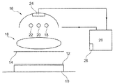
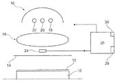
- 複数のLED(18、20、22)を含むフォトリソグラフィ露光システムの光源(16)を調整する方法であって、
特定の波長範囲で個々のLED(18、20、22)の光出力を検出する工程と、
検出した光出力を、全体のスペクトルについて、所望の光出力分布と比較する工程と、
LED(18、20、22)が操作されて、可能な最も正確な方法で、所望のスペクトルの光出力分布が達成される工程と、を含む方法。 - より高出力のLED(18、20、22)が、最も弱いLED(18、20、22)の光出力に適応されることを特徴とする請求項1に記載の方法。
- 光出力は、スペクトル選択センサ(24)の手段により測定されることを特徴とする請求項1または2に記載の方法。
- LED(18、20、22)は次から次に切り換えられ、光出力は広帯域センサ(24)の手段により測定されることを特徴とする請求項1または2に記載の方法。
- LED(18、20、22)の光出力は、較正工程で測定されることを特徴とする請求項1〜4のいずれかに記載の方法。
- 個々のLED(18、20、22)の加熱特性が測定されることを特徴とする請求項1〜5のいずれかに記載の方法。
- LED(18、20、22)は、一定の電力で操作されることを特徴とする請求項1〜6のいずれかに記載の方法。
- LED(18、20、22)は、調整された電力を用いて操作されることを特徴とする請求項1〜6のいずれかに記載の方法。
- LED(18、20、22)のエージングが、蓄積された典型的なエージング特性と比較されることを特徴とする請求項1〜8のいずれかに記載の方法。
- LED(18、20、22)の光出力が、予め定められた最小光出力と比較されることを特徴とする請求項1〜9のいずれかに記載の方法。
- LED(18、20、22)の光出力がいつ臨界値に到達するかを、ユーザは知らされることを特徴とする請求項9または10に記載の方法。
- フォトリソグラフィデバイスのための露光アセンブリであって、複数のLED(18、20、22)を含む光源、個々のLED(18、20、22)に供給される電力を制御する制御手段(26)、およびそれぞれの波長範囲で、LED(18、20、22)の光出力を検出できるセンサ(24)を有する露光アセンブリ。
- センサ(24)は、スペクトル選択センサであることを特徴とする請求項12に記載の露光アセンブリ。
- センサ(24)は、広帯域センサであることを特徴とする請求項12に記載の露光アセンブリ。
- センサ(24)は、光源(16)に組み込まれたことを特徴とする請求項12〜14のいずれかに記載の露光アセンブリ。
- センサ(24)は、フォトリソグラフィデバイスのレンズ(16)の上に配置されることを特徴とする請求項12〜14のいずれかに記載の露光アセンブリ。
- 制御手段(26)は、LED(18、20、22)の加熱特性を蓄積するためのメモリ(28)を含むことを特徴とする請求項12〜16のいずれかに記載の露光アセンブリ。
- 制御手段(26)は、LED(18、20、22)のエージング特性を蓄積するためのメモリ(28)を含み、その中にLEDのエージング特性が書き込まれることを特徴とする請求項12〜17のいずれかに記載の露光アセンブリ。
Applications Claiming Priority (2)
| Application Number | Priority Date | Filing Date | Title |
|---|---|---|---|
| NL2014572 | 2015-04-01 | ||
| NL2014572A NL2014572B1 (en) | 2015-04-01 | 2015-04-01 | Method for regulating a light source of a photolithography exposure system and exposure assembly for a photolithography device. |
Publications (1)
| Publication Number | Publication Date |
|---|---|
| JP2016194673A true JP2016194673A (ja) | 2016-11-17 |
Family
ID=53610941
Family Applications (1)
| Application Number | Title | Priority Date | Filing Date |
|---|---|---|---|
| JP2016018585A Pending JP2016194673A (ja) | 2015-04-01 | 2016-02-03 | フォトリソグラフィ露光システムの光源の調整方法およびフォトリソグラフィデバイス用の露光アセンブリ |
Country Status (8)
| Country | Link |
|---|---|
| US (1) | US9864277B2 (ja) |
| JP (1) | JP2016194673A (ja) |
| KR (1) | KR20160118134A (ja) |
| CN (1) | CN106054536A (ja) |
| AT (1) | AT516990B1 (ja) |
| DE (1) | DE102016106014A1 (ja) |
| NL (1) | NL2014572B1 (ja) |
| TW (1) | TWI695229B (ja) |
Families Citing this family (3)
| Publication number | Priority date | Publication date | Assignee | Title |
|---|---|---|---|---|
| US10558125B2 (en) * | 2016-11-17 | 2020-02-11 | Tokyo Electron Limited | Exposure apparatus, exposure apparatus adjustment method and storage medium |
| JP6866631B2 (ja) * | 2016-12-20 | 2021-04-28 | 東京エレクトロン株式会社 | 光処理装置、塗布、現像装置、光処理方法及び記憶媒体 |
| CN116610007B (zh) * | 2023-07-18 | 2023-10-27 | 上海图双精密装备有限公司 | 掩模对准光刻设备及其照明系统和照明方法 |
Citations (5)
| Publication number | Priority date | Publication date | Assignee | Title |
|---|---|---|---|---|
| JP2003163158A (ja) * | 2001-11-29 | 2003-06-06 | Pentax Corp | 露光装置用光源システムおよび露光装置 |
| JP2007053366A (ja) * | 2005-08-15 | 2007-03-01 | Avago Technologies Ecbu Ip (Singapore) Pte Ltd | 較正機能付きled光モジュール |
| US20080111983A1 (en) * | 2005-01-14 | 2008-05-15 | Carl Zeiss Smt Ag | Illumination System for a Microlithographic Projection Exposure Apparatus |
| JP2009139162A (ja) * | 2007-12-05 | 2009-06-25 | Sharp Corp | 検査用光源装置およびそれを用いた照度センサの検査方法 |
| JP2010045356A (ja) * | 2008-08-14 | 2010-02-25 | Asml Netherlands Bv | リソグラフィ装置及び方法 |
Family Cites Families (9)
| Publication number | Priority date | Publication date | Assignee | Title |
|---|---|---|---|---|
| JP2007329432A (ja) * | 2006-06-09 | 2007-12-20 | Canon Inc | 露光装置 |
| JP2009076688A (ja) * | 2007-09-20 | 2009-04-09 | Canon Inc | 露光装置及びデバイスの製造方法 |
| US7671542B2 (en) * | 2007-11-07 | 2010-03-02 | Au Optronics Corporation | Color control of multi-zone LED backlight |
| JP5361239B2 (ja) * | 2008-04-09 | 2013-12-04 | キヤノン株式会社 | 露光装置及びデバイス製造方法 |
| US20100283978A1 (en) * | 2009-05-07 | 2010-11-11 | Ultratech,Inc. | LED-based UV illuminators and lithography systems using same |
| US8520186B2 (en) * | 2009-08-25 | 2013-08-27 | Cymer, Llc | Active spectral control of optical source |
| KR101898921B1 (ko) * | 2011-11-16 | 2018-09-17 | 삼성디스플레이 주식회사 | 노광 시스템 이를 이용한 패턴 형성 방법 및 표시 기판의 제조 방법 |
| US9766275B2 (en) * | 2013-06-04 | 2017-09-19 | Applied Materials, Inc. | Methods and apparatus for increasing accuracy of RMS measurements of signals with a high crest factor |
| CN204143154U (zh) * | 2014-10-11 | 2015-02-04 | 叙丰企业股份有限公司 | 曝光机光源照射强度调整机构 |
-
2015
- 2015-04-01 NL NL2014572A patent/NL2014572B1/en not_active IP Right Cessation
-
2016
- 2016-02-02 TW TW105103332A patent/TWI695229B/zh not_active IP Right Cessation
- 2016-02-03 JP JP2016018585A patent/JP2016194673A/ja active Pending
- 2016-02-16 CN CN201610088033.5A patent/CN106054536A/zh active Pending
- 2016-03-01 AT AT501552016A patent/AT516990B1/de not_active IP Right Cessation
- 2016-03-10 US US15/066,676 patent/US9864277B2/en not_active Expired - Fee Related
- 2016-03-23 KR KR1020160034692A patent/KR20160118134A/ko not_active Withdrawn
- 2016-04-01 DE DE102016106014.3A patent/DE102016106014A1/de not_active Withdrawn
Patent Citations (5)
| Publication number | Priority date | Publication date | Assignee | Title |
|---|---|---|---|---|
| JP2003163158A (ja) * | 2001-11-29 | 2003-06-06 | Pentax Corp | 露光装置用光源システムおよび露光装置 |
| US20080111983A1 (en) * | 2005-01-14 | 2008-05-15 | Carl Zeiss Smt Ag | Illumination System for a Microlithographic Projection Exposure Apparatus |
| JP2007053366A (ja) * | 2005-08-15 | 2007-03-01 | Avago Technologies Ecbu Ip (Singapore) Pte Ltd | 較正機能付きled光モジュール |
| JP2009139162A (ja) * | 2007-12-05 | 2009-06-25 | Sharp Corp | 検査用光源装置およびそれを用いた照度センサの検査方法 |
| JP2010045356A (ja) * | 2008-08-14 | 2010-02-25 | Asml Netherlands Bv | リソグラフィ装置及び方法 |
Also Published As
| Publication number | Publication date |
|---|---|
| AT516990A3 (de) | 2019-07-15 |
| NL2014572A (en) | 2016-10-10 |
| AT516990A2 (de) | 2016-10-15 |
| KR20160118134A (ko) | 2016-10-11 |
| NL2014572B1 (en) | 2017-01-06 |
| AT516990B1 (de) | 2019-11-15 |
| TWI695229B (zh) | 2020-06-01 |
| CN106054536A (zh) | 2016-10-26 |
| US9864277B2 (en) | 2018-01-09 |
| US20160291480A1 (en) | 2016-10-06 |
| DE102016106014A1 (de) | 2016-10-06 |
| TW201708969A (zh) | 2017-03-01 |
Similar Documents
| Publication | Publication Date | Title |
|---|---|---|
| KR102246340B1 (ko) | 광원의 노광량 제어를 위한 방법 및 장치 | |
| JP2016194673A (ja) | フォトリソグラフィ露光システムの光源の調整方法およびフォトリソグラフィデバイス用の露光アセンブリ | |
| CN102023488A (zh) | 监测光刻工艺曝光机的能量偏移的方法 | |
| JP5957262B2 (ja) | 放電ランプを備えた照明装置 | |
| KR102043606B1 (ko) | 플래시램프 제어시스템 및 플래시램프를 제어하는 방법 | |
| JP7266194B2 (ja) | 照明システム及び照明システムの制御方法 | |
| CN107168016B (zh) | 光源装置以及具备该光源装置的曝光装置 | |
| CN116610007B (zh) | 掩模对准光刻设备及其照明系统和照明方法 | |
| KR101867527B1 (ko) | 측광 장치 및 노광 장치 | |
| JP7766861B2 (ja) | 照明装置キャリブレーション方法及び照明システム | |
| JP4352393B2 (ja) | 光源装置 | |
| KR101557769B1 (ko) | 복사조도 측정장치 및 그 측정방법 | |
| US7423729B2 (en) | Method of monitoring the light integrator of a photolithography system | |
| KR20020078200A (ko) | 노광량 조절 시스템 | |
| JP2014160780A5 (ja) | ||
| JPH036011A (ja) | 半導体装置製造用ウェーハ露光装置 | |
| KR101837061B1 (ko) | 적분구 시스템 및 피코 암페어 미터의 신뢰성 평가장치 | |
| KR100970736B1 (ko) | 보조광 트리거 시간 조정에 의한 연속 사진 촬영 방법 및이를 수행하는 카메라 | |
| KR101656702B1 (ko) | 적분구 시스템 신뢰성 평가장치 및 적분구 시스템 신뢰성 평가방법 | |
| JP2000208386A (ja) | 露光装置および露光装置の照度均一性調整方法 | |
| JPS61267323A (ja) | 半導体装置製造用露光装置 | |
| KR20160096828A (ko) | 종점 검출장치 및 이의 제어 방법 |
Legal Events
| Date | Code | Title | Description |
|---|---|---|---|
| A621 | Written request for application examination |
Free format text: JAPANESE INTERMEDIATE CODE: A621 Effective date: 20181211 |
|
| A977 | Report on retrieval |
Free format text: JAPANESE INTERMEDIATE CODE: A971007 Effective date: 20191017 |
|
| A131 | Notification of reasons for refusal |
Free format text: JAPANESE INTERMEDIATE CODE: A131 Effective date: 20191029 |
|
| A601 | Written request for extension of time |
Free format text: JAPANESE INTERMEDIATE CODE: A601 Effective date: 20200128 |
|
| A521 | Request for written amendment filed |
Free format text: JAPANESE INTERMEDIATE CODE: A523 Effective date: 20200330 |
|
| A02 | Decision of refusal |
Free format text: JAPANESE INTERMEDIATE CODE: A02 Effective date: 20200707 |