JP2016162964A - 半導体装置の製造方法および半導体装置 - Google Patents
半導体装置の製造方法および半導体装置 Download PDFInfo
- Publication number
- JP2016162964A JP2016162964A JP2015042542A JP2015042542A JP2016162964A JP 2016162964 A JP2016162964 A JP 2016162964A JP 2015042542 A JP2015042542 A JP 2015042542A JP 2015042542 A JP2015042542 A JP 2015042542A JP 2016162964 A JP2016162964 A JP 2016162964A
- Authority
- JP
- Japan
- Prior art keywords
- semiconductor device
- sealing structure
- grinding
- back surface
- mold
- Prior art date
- Legal status (The legal status is an assumption and is not a legal conclusion. Google has not performed a legal analysis and makes no representation as to the accuracy of the status listed.)
- Pending
Links
Images


Classifications
-
- H—ELECTRICITY
- H01—ELECTRIC ELEMENTS
- H01L—SEMICONDUCTOR DEVICES NOT COVERED BY CLASS H10
- H01L2224/00—Indexing scheme for arrangements for connecting or disconnecting semiconductor or solid-state bodies and methods related thereto as covered by H01L24/00
- H01L2224/01—Means for bonding being attached to, or being formed on, the surface to be connected, e.g. chip-to-package, die-attach, "first-level" interconnects; Manufacturing methods related thereto
- H01L2224/26—Layer connectors, e.g. plate connectors, solder or adhesive layers; Manufacturing methods related thereto
- H01L2224/31—Structure, shape, material or disposition of the layer connectors after the connecting process
- H01L2224/32—Structure, shape, material or disposition of the layer connectors after the connecting process of an individual layer connector
- H01L2224/321—Disposition
- H01L2224/32151—Disposition the layer connector connecting between a semiconductor or solid-state body and an item not being a semiconductor or solid-state body, e.g. chip-to-substrate, chip-to-passive
- H01L2224/32221—Disposition the layer connector connecting between a semiconductor or solid-state body and an item not being a semiconductor or solid-state body, e.g. chip-to-substrate, chip-to-passive the body and the item being stacked
- H01L2224/32245—Disposition the layer connector connecting between a semiconductor or solid-state body and an item not being a semiconductor or solid-state body, e.g. chip-to-substrate, chip-to-passive the body and the item being stacked the item being metallic
-
- H—ELECTRICITY
- H01—ELECTRIC ELEMENTS
- H01L—SEMICONDUCTOR DEVICES NOT COVERED BY CLASS H10
- H01L2224/00—Indexing scheme for arrangements for connecting or disconnecting semiconductor or solid-state bodies and methods related thereto as covered by H01L24/00
- H01L2224/01—Means for bonding being attached to, or being formed on, the surface to be connected, e.g. chip-to-package, die-attach, "first-level" interconnects; Manufacturing methods related thereto
- H01L2224/42—Wire connectors; Manufacturing methods related thereto
- H01L2224/47—Structure, shape, material or disposition of the wire connectors after the connecting process
- H01L2224/48—Structure, shape, material or disposition of the wire connectors after the connecting process of an individual wire connector
- H01L2224/4805—Shape
- H01L2224/4809—Loop shape
- H01L2224/48091—Arched
-
- H—ELECTRICITY
- H01—ELECTRIC ELEMENTS
- H01L—SEMICONDUCTOR DEVICES NOT COVERED BY CLASS H10
- H01L2224/00—Indexing scheme for arrangements for connecting or disconnecting semiconductor or solid-state bodies and methods related thereto as covered by H01L24/00
- H01L2224/01—Means for bonding being attached to, or being formed on, the surface to be connected, e.g. chip-to-package, die-attach, "first-level" interconnects; Manufacturing methods related thereto
- H01L2224/42—Wire connectors; Manufacturing methods related thereto
- H01L2224/47—Structure, shape, material or disposition of the wire connectors after the connecting process
- H01L2224/48—Structure, shape, material or disposition of the wire connectors after the connecting process of an individual wire connector
- H01L2224/481—Disposition
- H01L2224/48151—Connecting between a semiconductor or solid-state body and an item not being a semiconductor or solid-state body, e.g. chip-to-substrate, chip-to-passive
- H01L2224/48221—Connecting between a semiconductor or solid-state body and an item not being a semiconductor or solid-state body, e.g. chip-to-substrate, chip-to-passive the body and the item being stacked
- H01L2224/48245—Connecting between a semiconductor or solid-state body and an item not being a semiconductor or solid-state body, e.g. chip-to-substrate, chip-to-passive the body and the item being stacked the item being metallic
- H01L2224/48247—Connecting between a semiconductor or solid-state body and an item not being a semiconductor or solid-state body, e.g. chip-to-substrate, chip-to-passive the body and the item being stacked the item being metallic connecting the wire to a bond pad of the item
-
- H—ELECTRICITY
- H01—ELECTRIC ELEMENTS
- H01L—SEMICONDUCTOR DEVICES NOT COVERED BY CLASS H10
- H01L2224/00—Indexing scheme for arrangements for connecting or disconnecting semiconductor or solid-state bodies and methods related thereto as covered by H01L24/00
- H01L2224/01—Means for bonding being attached to, or being formed on, the surface to be connected, e.g. chip-to-package, die-attach, "first-level" interconnects; Manufacturing methods related thereto
- H01L2224/42—Wire connectors; Manufacturing methods related thereto
- H01L2224/47—Structure, shape, material or disposition of the wire connectors after the connecting process
- H01L2224/49—Structure, shape, material or disposition of the wire connectors after the connecting process of a plurality of wire connectors
- H01L2224/491—Disposition
- H01L2224/4912—Layout
- H01L2224/49171—Fan-out arrangements
-
- H—ELECTRICITY
- H01—ELECTRIC ELEMENTS
- H01L—SEMICONDUCTOR DEVICES NOT COVERED BY CLASS H10
- H01L2224/00—Indexing scheme for arrangements for connecting or disconnecting semiconductor or solid-state bodies and methods related thereto as covered by H01L24/00
- H01L2224/73—Means for bonding being of different types provided for in two or more of groups H01L2224/10, H01L2224/18, H01L2224/26, H01L2224/34, H01L2224/42, H01L2224/50, H01L2224/63, H01L2224/71
- H01L2224/732—Location after the connecting process
- H01L2224/73251—Location after the connecting process on different surfaces
- H01L2224/73265—Layer and wire connectors
-
- H—ELECTRICITY
- H01—ELECTRIC ELEMENTS
- H01L—SEMICONDUCTOR DEVICES NOT COVERED BY CLASS H10
- H01L2224/00—Indexing scheme for arrangements for connecting or disconnecting semiconductor or solid-state bodies and methods related thereto as covered by H01L24/00
- H01L2224/93—Batch processes
- H01L2224/95—Batch processes at chip-level, i.e. with connecting carried out on a plurality of singulated devices, i.e. on diced chips
- H01L2224/97—Batch processes at chip-level, i.e. with connecting carried out on a plurality of singulated devices, i.e. on diced chips the devices being connected to a common substrate, e.g. interposer, said common substrate being separable into individual assemblies after connecting
-
- H—ELECTRICITY
- H01—ELECTRIC ELEMENTS
- H01L—SEMICONDUCTOR DEVICES NOT COVERED BY CLASS H10
- H01L2924/00—Indexing scheme for arrangements or methods for connecting or disconnecting semiconductor or solid-state bodies as covered by H01L24/00
- H01L2924/15—Details of package parts other than the semiconductor or other solid state devices to be connected
- H01L2924/181—Encapsulation
Abstract
Description
前記方法において、前記個片化工程は、前記封止構造の表面および裏面に対して垂直な方向に前記封止構造を選択的に切断する工程を含むことが好ましい。この方法によれば、表面および裏面に対して垂直な方向に封止構造を切断すればよいので、封止構造から複数の半導体装置の個片を容易に切り出すことができる。これにより、異なる大きさおよび形状を有する種々の半導体装置を共通の金型で容易に製造できる。
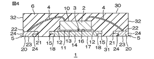
図1は、本発明の一実施形態に係る製造方法が適用された一の例に係る半導体装置1を示す斜視図である。図2は、図1に示す半導体装置1の底面図である。図3は、図1に示す半導体装置1の内部構造を示す平面図である。図4は、図3に示すIV-IV線に沿う断面図である。
パッド抜け抑制部15は、パッド本体部14の側面18からリード5側に向けて張り出すように形成されている。パッド抜け抑制部15は、パッド本体部14の上面16と面一に形成され、パッド本体部14よりも小さい厚さを有している。パッド抜け抑制部15およびパッド本体部14の側面18により形成された段差部分に封止樹脂6が入り込むことにより、パッド本体部14の封止樹脂6からの脱落が抑制される。
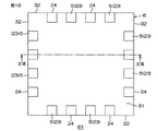
複数のリード5は、ダイパッド3の周囲4方向に、ダイパッド3から間隔を空けてそれぞれ配置されている。各リード5は、その整列方向に直交する方向に長尺な直方体形状のリード本体部20と、リード抜け抑制部21とを一体的に有している。リード本体部20は、上面22と、上面22の反対側に位置する下面23と、上面22と下面23とを接続する4つの側面24とを含む。リード5は、リード本体部20の上面22に接続されたボンディングワイヤ4を介して、半導体チップ2に電気的に接続される。
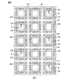
図6に示すように、リードフレーム40は、たとえば、銅板、42アロイ板等の金属薄板であり、プレス加工により形成されている。リードフレーム40は、複数のダイパッド3と、各ダイパッド3から間隔を空けて各ダイパッド3の周囲4方向に配置された複数のリード5と、各ダイパッド3および各リード5を支持するフレーム部41とを含む。
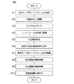
次に、図8に示すように、各ダイパッド3に半導体チップ2が配置される(ステップS2)。各半導体チップ2は、半田等の金属膜13により、各ダイパッド3の上面16に固定される。次に、ボンディングワイヤ4が、半導体チップ2および対応するリード5に接続される(ステップS3)。これにより、半導体チップ2が、リード5に電気的に接続される。
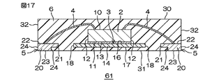
次に、図10に示すように、リードフレーム40を被覆するように、金型50内に封止樹脂6が流し込まれる(ステップS5)。これにより、封止樹脂6により複数の半導体チップ2が一括して被覆される。その後、封止樹脂6が硬化(熱硬化)される。これにより、封止構造55が形成される。封止構造55は、複数の半導体チップ2を一括して封止しており、表面56と、表面56の反対側に位置し、各ダイパッド3の下面17および各リード5の下面23が封止樹脂6から露出する裏面57とを有している。封止構造55は、一対の上型51および下型52に対応した一様な厚さを有している。支持テープ44が封止構造55の裏面57に貼付されている状態では、複数のダイパッド3の裏面57は外部に露出していない。
次に、図12に示すように、封止構造55の表面56が研削される(ステップS8)。より具体的には、封止構造55の表面56は、化学的機械的研磨法により研磨される。これにより、封止構造55が目的とする厚さまで研磨される。
この裏面研削工程において、各ダイパッド3の下面17および各リード5の下面23を含む封止構造55の裏面57に、研削による研削痕(図示せず)が形成される。封止構造55の裏面57の研削痕は、より具体的には、化学的機械的研磨法による研磨痕である。この裏面研削工程では、封止構造55の裏面57に、高低差が10μm以下の凹凸を含む研削痕(研磨痕)が形成される。すなわち、封止構造55の裏面57は、表面粗さが10μm以下になるように研削(研磨)される。さらに具体的には、封止構造55の裏面57に、高低差が5μm以下の凹凸を含む研削痕(研磨痕)が形成される。すなわち、封止構造55の裏面57は、表面粗さが5μm以下になるように研削(研磨)される。封止構造55は、化学的機械的研磨法により、その裏面57が鏡面化されてもよい。この場合、封止構造55の裏面57の研削痕は、鏡面化研磨加工による鏡面研磨痕である。
次に、図15に示すように、ダイシングライン43に沿って封止構造55がダイシングソー58により切断される(ステップS10)。この際、封止構造55は、表面56および裏面57に対して垂直な方向に切断される。これにより、封止構造55の表面56が封止樹脂6の表面30となり、封止構造55の裏面57が封止樹脂6の裏面31となる。そして、封止構造55のダイシングソー58により切断された部分が封止樹脂6の側面32となる。このようにして、封止構造55から複数の半導体装置1の個片が切り出される。
半導体装置61は、封止樹脂6により覆われた下面17を有するダイパッド3を含む点で、前述の半導体装置1と異なる。すなわち、半導体装置61では、ダイパッド3の下面17が、封止樹脂6の裏面31から露出していない。この場合、半導体チップ2は、ダイパッド3と、ダイパッド3に接続されたボンディングワイヤ4を介して対応するリード5と電気的に接続される。
前述の各例では、半導体装置1,61が、ダイパッド3の周囲4方向のそれぞれにリード5が配置されたQFNタイプである例について説明した。しかし、半導体装置1,61は、ダイパッド3の周囲のいずれか2方向(たとえば、ダイパッド3の互いに対向する二つの側面18に沿う方向)のみにリード5が配置されたDFN(Dual Flat Non lead package)タイプであってもよい。この場合、図18および図19に示す例を採用してもよい。
半導体装置63は、ほぼ直方体形状のDFNタイプの半導体装置である。半導体装置63は、封止樹脂6により被覆された下面17を有するダイパッド3と、ダイパッド3の互いに対向する二つの側面18に沿って配置された一対のリード5A,5Bとを有している。以下では、説明の便宜上、一方側のリード5Aを「入力端子5A」といい、他方側のリード5Bを「出力端子5B」という。
リードフレーム65は、複数のダイパッド3と、各ダイパッド3を挟んで互いに対向する一対の入力端子5Aおよび出力端子5Bと、各ダイパッド3と出力端子5Bとを接続する接続部64と、入力端子5Aおよび出力端子5Bを支持するフレーム部41とを有している。ダイシングライン43(二点鎖線参照)は、フレーム部41に沿い、フレーム部41よりも幅広に設定されている。列方向に沿って設定されたダイシングライン43は、入力端子5Aおよび出力端子5Bを、それらが延びる方向に直交する方向に横切っている。
たとえば、前述の実施形態では、表面研削工程(ステップS8)および裏面研削工程(ステップS9)の両方を実施する例について説明した。しかし、図21に示すように、表面研削工程(ステップS8)および裏面研削工程(ステップS9)のいずれか一方のみを実施するようにしてもよい。この場合、個片化工程(ステップS10)が実施されると、封止樹脂6の表面30が、封止樹脂6の裏面31と異なる表面粗さを有する半導体装置1が製造される。
また、前述の各実施形態では、半導体チップ2の裏面11が、ダイパッド3の上面16に接合される例について説明したが、半導体チップ2は、素子形成面10がダイパッド3の上面16に接合されるように、ダイパッド3上に配置(フリップチップ接合)されてもよい。
2 半導体チップ
3 ダイパッド
4 ボンディングワイヤ(配線部材)
5 リード
6 封止樹脂
30 封止樹脂の表面
31 封止樹脂の裏面
32 封止樹脂の側面
40 リードフレーム
50 金型
51 上型
52 下型
55 封止構造
56 封止構造の表面
57 封止構造の裏面
61 半導体装置
63 半導体装置
65 リードフレーム
Claims (15)
- 複数のダイパッドおよびリードを含むリードフレームにおいて、各前記ダイパッドに半導体チップを配置する工程と、
前記リードと前記半導体チップとを配線部材を介して電気的に接続する工程と、
前記リードフレームを金型内に配置し、前記金型に封止樹脂を流し込むことにより、複数の前記半導体チップが一括封止された封止構造を形成する工程と、
前記封止構造を研削して、前記封止構造を薄化する薄化工程と、
前記封止構造を選択的に切断して、半導体装置の個片を切り出す個片化工程とを含む、半導体装置の製造方法。 - 前記金型は、少なくとも前記リードフレームが配置される領域を一様な高さで挟み込む一対の上型および下型を有しており、
前記封止構造を形成する工程は、一様な厚さを有する前記封止構造を形成する工程を含む、請求項1に記載の半導体装置の製造方法。 - 前記封止構造が、少なくとも前記リードの下面が露出する裏面と、その反対側に位置する表面とを有し、
前記薄化工程は、前記封止構造の表面を研削する表面研削工程を含む、請求項1または2に記載の半導体装置の製造方法。 - 前記表面研削工程において、高低差が10μm以下の凹凸を含む研削痕が前記封止構造の表面に形成される、請求項3に記載の半導体装置の製造方法。
- 前記表面研削工程において、高低差が5μm以下の凹凸を含む研削痕が前記封止構造の表面に形成される、請求項4に記載の半導体装置の製造方法。
- 前記表面研削工程は、化学的機械的研磨法により、前記封止構造の表面を研磨する表面研磨工程を含む、請求項3〜5のいずれか一項に記載の半導体装置の製造方法。
- 前記封止構造が、少なくとも前記リードの下面が露出する裏面と、その反対側に位置する表面とを有し、
前記薄化工程は、前記封止構造の裏面を研削する裏面研削工程を含む、請求項1〜6のいずれか一項に記載の半導体装置の製造方法。 - 前記裏面研削工程は、化学的機械的研磨法により、前記封止構造の裏面を研磨する裏面研磨工程を含む、請求項7に記載の半導体装置の製造方法。
- 前記個片化工程は、前記封止構造の表面および裏面に対して垂直な方向に前記封止構造を選択的に切断する工程を含む、請求項1〜8のいずれか一項に記載の半導体装置の製造方法。
- 半導体チップと、
前記半導体チップを支持するダイパッドと、
前記ダイパッドの周囲に配置され、配線部材を介して前記半導体チップに電気的に接続されたリードと、
前記半導体チップ、前記ダイパッドおよび前記リードを封止し、表面と、その反対側に位置し、少なくとも前記リードの下面が露出する裏面とを有する封止樹脂とを含み、
前記封止樹脂の表面は、研削されることにより形成された表面側研削痕を有している、半導体装置。 - 前記表面側研削痕は、高低差が10μm以下の凹凸を含む、請求項10に記載の半導体装置。
- 前記表面側研削痕は、高低差が5μm以下の凹凸を含む、請求項11に記載の半導体装置。
- 前記表面側研削痕は、表面以外の面の粗さよりも小さい粗さを含む、請求項10〜12のいずれか一項に記載の半導体装置。
- 前記封止樹脂は、前記封止樹脂の表面および裏面のそれぞれに対して垂直に形成された側面を有している、請求項10〜13のいずれか一項に記載の半導体装置。
- 前記封止樹脂の裏面は、研削されることにより形成された裏面側研削痕を有している、請求項10〜14のいずれか一項に記載の半導体装置。
Priority Applications (1)
| Application Number | Priority Date | Filing Date | Title |
|---|---|---|---|
| JP2015042542A JP2016162964A (ja) | 2015-03-04 | 2015-03-04 | 半導体装置の製造方法および半導体装置 |
Applications Claiming Priority (1)
| Application Number | Priority Date | Filing Date | Title |
|---|---|---|---|
| JP2015042542A JP2016162964A (ja) | 2015-03-04 | 2015-03-04 | 半導体装置の製造方法および半導体装置 |
Publications (1)
| Publication Number | Publication Date |
|---|---|
| JP2016162964A true JP2016162964A (ja) | 2016-09-05 |
Family
ID=56847580
Family Applications (1)
| Application Number | Title | Priority Date | Filing Date |
|---|---|---|---|
| JP2015042542A Pending JP2016162964A (ja) | 2015-03-04 | 2015-03-04 | 半導体装置の製造方法および半導体装置 |
Country Status (1)
| Country | Link |
|---|---|
| JP (1) | JP2016162964A (ja) |
Cited By (3)
| Publication number | Priority date | Publication date | Assignee | Title |
|---|---|---|---|---|
| JP6283131B1 (ja) * | 2017-01-31 | 2018-02-21 | 株式会社加藤電器製作所 | 電子デバイス及び電子デバイスの製造方法 |
| JP2018064089A (ja) * | 2016-10-13 | 2018-04-19 | 芝浦メカトロニクス株式会社 | 電子部品、電子部品の製造装置及び電子部品の製造方法 |
| WO2022070741A1 (ja) * | 2020-10-01 | 2022-04-07 | ローム株式会社 | 半導体装置 |
Citations (7)
| Publication number | Priority date | Publication date | Assignee | Title |
|---|---|---|---|---|
| JP2004079665A (ja) * | 2002-08-13 | 2004-03-11 | Seiko Epson Corp | 半導体製造装置および半導体装置の製造方法 |
| JP2004208326A (ja) * | 2000-03-17 | 2004-07-22 | Matsushita Electric Ind Co Ltd | 電気素子内蔵モジュール及びその製造方法 |
| JP2004235237A (ja) * | 2003-01-28 | 2004-08-19 | Sanyo Electric Co Ltd | 樹脂封止金型及びそれを用いた半導体装置の製造方法 |
| JP2005109300A (ja) * | 2003-10-01 | 2005-04-21 | Lintec Corp | 樹脂封止型の電子デバイスの製造方法。 |
| JP2012019098A (ja) * | 2010-07-08 | 2012-01-26 | Fuji Electric Co Ltd | 半導体装置の製造方法 |
| JP2013135143A (ja) * | 2011-12-27 | 2013-07-08 | Hitachi Chemical Co Ltd | 半導体装置の製造方法、それにより得られる半導体装置及びそれに用いる熱硬化性樹脂組成物 |
| JP2013239740A (ja) * | 2013-08-02 | 2013-11-28 | Rohm Co Ltd | 半導体装置 |
-
2015
- 2015-03-04 JP JP2015042542A patent/JP2016162964A/ja active Pending
Patent Citations (7)
| Publication number | Priority date | Publication date | Assignee | Title |
|---|---|---|---|---|
| JP2004208326A (ja) * | 2000-03-17 | 2004-07-22 | Matsushita Electric Ind Co Ltd | 電気素子内蔵モジュール及びその製造方法 |
| JP2004079665A (ja) * | 2002-08-13 | 2004-03-11 | Seiko Epson Corp | 半導体製造装置および半導体装置の製造方法 |
| JP2004235237A (ja) * | 2003-01-28 | 2004-08-19 | Sanyo Electric Co Ltd | 樹脂封止金型及びそれを用いた半導体装置の製造方法 |
| JP2005109300A (ja) * | 2003-10-01 | 2005-04-21 | Lintec Corp | 樹脂封止型の電子デバイスの製造方法。 |
| JP2012019098A (ja) * | 2010-07-08 | 2012-01-26 | Fuji Electric Co Ltd | 半導体装置の製造方法 |
| JP2013135143A (ja) * | 2011-12-27 | 2013-07-08 | Hitachi Chemical Co Ltd | 半導体装置の製造方法、それにより得られる半導体装置及びそれに用いる熱硬化性樹脂組成物 |
| JP2013239740A (ja) * | 2013-08-02 | 2013-11-28 | Rohm Co Ltd | 半導体装置 |
Cited By (7)
| Publication number | Priority date | Publication date | Assignee | Title |
|---|---|---|---|---|
| JP2018064089A (ja) * | 2016-10-13 | 2018-04-19 | 芝浦メカトロニクス株式会社 | 電子部品、電子部品の製造装置及び電子部品の製造方法 |
| JP7039224B2 (ja) | 2016-10-13 | 2022-03-22 | 芝浦メカトロニクス株式会社 | 電子部品の製造装置及び電子部品の製造方法 |
| JP6283131B1 (ja) * | 2017-01-31 | 2018-02-21 | 株式会社加藤電器製作所 | 電子デバイス及び電子デバイスの製造方法 |
| JP2018125403A (ja) * | 2017-01-31 | 2018-08-09 | 株式会社加藤電器製作所 | 電子デバイス及び電子デバイスの製造方法 |
| US10242937B2 (en) | 2017-01-31 | 2019-03-26 | Katoh Electric Co, Ltd. | Electronic device and method for manufacturing electronic device |
| US10707156B2 (en) | 2017-01-31 | 2020-07-07 | Katoh Electric Co., Ltd. | Electronic device |
| WO2022070741A1 (ja) * | 2020-10-01 | 2022-04-07 | ローム株式会社 | 半導体装置 |
Similar Documents
| Publication | Publication Date | Title |
|---|---|---|
| US8836101B2 (en) | Multi-chip semiconductor packages and assembly thereof | |
| US11908777B2 (en) | Semiconductor package with plurality of leads and sealing resin | |
| US6909168B2 (en) | Resin encapsulation semiconductor device utilizing grooved leads and die pad | |
| CN209785926U (zh) | 半导体器件 | |
| US7902649B2 (en) | Leadframe for leadless package, structure and manufacturing method using the same | |
| JPH11312706A (ja) | 樹脂封止型半導体装置及びその製造方法、リードフレーム | |
| US20050051877A1 (en) | Semiconductor package having high quantity of I/O connections and method for fabricating the same | |
| KR101440933B1 (ko) | 범프 기술을 이용하는 ic 패키지 시스템 | |
| US20180122731A1 (en) | Plated ditch pre-mold lead frame, semiconductor package, and method of making same | |
| JP3837215B2 (ja) | 個別半導体装置およびその製造方法 | |
| US20180158758A1 (en) | Leadframe and method of manufacturing the same | |
| US10707158B2 (en) | Package with vertical interconnect between carrier and clip | |
| TW201802956A (zh) | 形成具有導電的互連框的半導體封裝之方法及結構 | |
| US9786583B2 (en) | Power semiconductor package device having locking mechanism, and preparation method thereof | |
| JP4373122B2 (ja) | 樹脂封止型半導体装置とその製造方法 | |
| JP2016162964A (ja) | 半導体装置の製造方法および半導体装置 | |
| US20210183799A1 (en) | Ultra-thin multichip power devices | |
| TW201539674A (zh) | 四方扁平無引腳封裝及其製造方法 | |
| US9209152B2 (en) | Molding material and method for packaging semiconductor chips | |
| US20190355651A1 (en) | Two sided bondable lead frame | |
| JP6490453B2 (ja) | 半導体装置の製造方法および半導体装置 | |
| US10840172B2 (en) | Leadframe, semiconductor package including a leadframe and method for forming a semiconductor package | |
| US20150097278A1 (en) | Surface mount semiconductor device with additional bottom face contacts | |
| US8080448B1 (en) | Semiconductor device with nested rows of contacts | |
| JP2017183417A (ja) | 半導体装置 |
Legal Events
| Date | Code | Title | Description |
|---|---|---|---|
| A621 | Written request for application examination |
Free format text: JAPANESE INTERMEDIATE CODE: A621 Effective date: 20180216 |
|
| A977 | Report on retrieval |
Free format text: JAPANESE INTERMEDIATE CODE: A971007 Effective date: 20181002 |
|
| A131 | Notification of reasons for refusal |
Free format text: JAPANESE INTERMEDIATE CODE: A131 Effective date: 20181004 |
|
| A521 | Request for written amendment filed |
Free format text: JAPANESE INTERMEDIATE CODE: A523 Effective date: 20181203 |
|
| A131 | Notification of reasons for refusal |
Free format text: JAPANESE INTERMEDIATE CODE: A131 Effective date: 20190221 |
|
| A521 | Request for written amendment filed |
Free format text: JAPANESE INTERMEDIATE CODE: A523 Effective date: 20190419 |
|
| A02 | Decision of refusal |
Free format text: JAPANESE INTERMEDIATE CODE: A02 Effective date: 20190711 |