JP2016081981A - Semiconductor device and manufacturing method of the same - Google Patents
Semiconductor device and manufacturing method of the same Download PDFInfo
- Publication number
- JP2016081981A JP2016081981A JP2014209618A JP2014209618A JP2016081981A JP 2016081981 A JP2016081981 A JP 2016081981A JP 2014209618 A JP2014209618 A JP 2014209618A JP 2014209618 A JP2014209618 A JP 2014209618A JP 2016081981 A JP2016081981 A JP 2016081981A
- Authority
- JP
- Japan
- Prior art keywords
- silicon oxide
- type
- oxide film
- region
- film
- Prior art date
- Legal status (The legal status is an assumption and is not a legal conclusion. Google has not performed a legal analysis and makes no representation as to the accuracy of the status listed.)
- Pending
Links
- 239000004065 semiconductor Substances 0.000 title claims abstract description 63
- 238000004519 manufacturing process Methods 0.000 title claims abstract description 21
- VYPSYNLAJGMNEJ-UHFFFAOYSA-N Silicium dioxide Chemical compound O=[Si]=O VYPSYNLAJGMNEJ-UHFFFAOYSA-N 0.000 claims abstract description 66
- 229910052814 silicon oxide Inorganic materials 0.000 claims abstract description 66
- 238000002161 passivation Methods 0.000 claims abstract description 64
- 238000000034 method Methods 0.000 claims description 15
- 230000003647 oxidation Effects 0.000 claims description 6
- 238000007254 oxidation reaction Methods 0.000 claims description 6
- 230000005684 electric field Effects 0.000 abstract description 17
- 230000015556 catabolic process Effects 0.000 abstract description 12
- XUIMIQQOPSSXEZ-UHFFFAOYSA-N Silicon Chemical compound [Si] XUIMIQQOPSSXEZ-UHFFFAOYSA-N 0.000 abstract description 9
- 229910052710 silicon Inorganic materials 0.000 abstract description 9
- 239000010703 silicon Substances 0.000 abstract description 9
- 230000002401 inhibitory effect Effects 0.000 abstract 1
- HBMJWWWQQXIZIP-UHFFFAOYSA-N silicon carbide Chemical compound [Si+]#[C-] HBMJWWWQQXIZIP-UHFFFAOYSA-N 0.000 description 25
- 229910010271 silicon carbide Inorganic materials 0.000 description 25
- 239000000758 substrate Substances 0.000 description 10
- 239000012535 impurity Substances 0.000 description 9
- 239000000463 material Substances 0.000 description 7
- 230000000903 blocking effect Effects 0.000 description 4
- 230000006378 damage Effects 0.000 description 4
- 238000005468 ion implantation Methods 0.000 description 3
- 238000004518 low pressure chemical vapour deposition Methods 0.000 description 3
- 238000000623 plasma-assisted chemical vapour deposition Methods 0.000 description 3
- 229910052782 aluminium Inorganic materials 0.000 description 2
- XAGFODPZIPBFFR-UHFFFAOYSA-N aluminium Chemical compound [Al] XAGFODPZIPBFFR-UHFFFAOYSA-N 0.000 description 2
- 230000004888 barrier function Effects 0.000 description 2
- 229910052751 metal Inorganic materials 0.000 description 2
- 239000002184 metal Substances 0.000 description 2
- OAICVXFJPJFONN-UHFFFAOYSA-N Phosphorus Chemical compound [P] OAICVXFJPJFONN-UHFFFAOYSA-N 0.000 description 1
- 239000000969 carrier Substances 0.000 description 1
- 239000002131 composite material Substances 0.000 description 1
- 239000012141 concentrate Substances 0.000 description 1
- 239000004020 conductor Substances 0.000 description 1
- 230000007423 decrease Effects 0.000 description 1
- 230000002542 deteriorative effect Effects 0.000 description 1
- 230000000694 effects Effects 0.000 description 1
- 229910044991 metal oxide Inorganic materials 0.000 description 1
- 150000004706 metal oxides Chemical class 0.000 description 1
- 238000012986 modification Methods 0.000 description 1
- 230000004048 modification Effects 0.000 description 1
- 229910052698 phosphorus Inorganic materials 0.000 description 1
- 239000011574 phosphorus Substances 0.000 description 1
- 229920006122 polyamide resin Polymers 0.000 description 1
- 229920001721 polyimide Polymers 0.000 description 1
- 239000009719 polyimide resin Substances 0.000 description 1
- 230000001681 protective effect Effects 0.000 description 1
- 239000011347 resin Substances 0.000 description 1
- 229920005989 resin Polymers 0.000 description 1
Images

Classifications
-
- H—ELECTRICITY
- H01—ELECTRIC ELEMENTS
- H01L—SEMICONDUCTOR DEVICES NOT COVERED BY CLASS H10
- H01L29/00—Semiconductor devices adapted for rectifying, amplifying, oscillating or switching, or capacitors or resistors with at least one potential-jump barrier or surface barrier, e.g. PN junction depletion layer or carrier concentration layer; Details of semiconductor bodies or of electrodes thereof ; Multistep manufacturing processes therefor
- H01L29/02—Semiconductor bodies ; Multistep manufacturing processes therefor
- H01L29/12—Semiconductor bodies ; Multistep manufacturing processes therefor characterised by the materials of which they are formed
- H01L29/16—Semiconductor bodies ; Multistep manufacturing processes therefor characterised by the materials of which they are formed including, apart from doping materials or other impurities, only elements of Group IV of the Periodic System
- H01L29/1608—Silicon carbide
-
- H—ELECTRICITY
- H01—ELECTRIC ELEMENTS
- H01L—SEMICONDUCTOR DEVICES NOT COVERED BY CLASS H10
- H01L21/00—Processes or apparatus adapted for the manufacture or treatment of semiconductor or solid state devices or of parts thereof
- H01L21/02—Manufacture or treatment of semiconductor devices or of parts thereof
- H01L21/02104—Forming layers
- H01L21/02365—Forming inorganic semiconducting materials on a substrate
- H01L21/02518—Deposited layers
- H01L21/02521—Materials
- H01L21/02524—Group 14 semiconducting materials
- H01L21/02529—Silicon carbide
-
- H—ELECTRICITY
- H01—ELECTRIC ELEMENTS
- H01L—SEMICONDUCTOR DEVICES NOT COVERED BY CLASS H10
- H01L21/00—Processes or apparatus adapted for the manufacture or treatment of semiconductor or solid state devices or of parts thereof
- H01L21/02—Manufacture or treatment of semiconductor devices or of parts thereof
- H01L21/02104—Forming layers
- H01L21/02107—Forming insulating materials on a substrate
- H01L21/02109—Forming insulating materials on a substrate characterised by the type of layer, e.g. type of material, porous/non-porous, pre-cursors, mixtures or laminates
- H01L21/02112—Forming insulating materials on a substrate characterised by the type of layer, e.g. type of material, porous/non-porous, pre-cursors, mixtures or laminates characterised by the material of the layer
- H01L21/02123—Forming insulating materials on a substrate characterised by the type of layer, e.g. type of material, porous/non-porous, pre-cursors, mixtures or laminates characterised by the material of the layer the material containing silicon
- H01L21/02164—Forming insulating materials on a substrate characterised by the type of layer, e.g. type of material, porous/non-porous, pre-cursors, mixtures or laminates characterised by the material of the layer the material containing silicon the material being a silicon oxide, e.g. SiO2
-
- H—ELECTRICITY
- H01—ELECTRIC ELEMENTS
- H01L—SEMICONDUCTOR DEVICES NOT COVERED BY CLASS H10
- H01L21/00—Processes or apparatus adapted for the manufacture or treatment of semiconductor or solid state devices or of parts thereof
- H01L21/02—Manufacture or treatment of semiconductor devices or of parts thereof
- H01L21/02104—Forming layers
- H01L21/02107—Forming insulating materials on a substrate
- H01L21/02225—Forming insulating materials on a substrate characterised by the process for the formation of the insulating layer
- H01L21/02227—Forming insulating materials on a substrate characterised by the process for the formation of the insulating layer formation by a process other than a deposition process
- H01L21/0223—Forming insulating materials on a substrate characterised by the process for the formation of the insulating layer formation by a process other than a deposition process formation by oxidation, e.g. oxidation of the substrate
- H01L21/02233—Forming insulating materials on a substrate characterised by the process for the formation of the insulating layer formation by a process other than a deposition process formation by oxidation, e.g. oxidation of the substrate of the semiconductor substrate or a semiconductor layer
- H01L21/02236—Forming insulating materials on a substrate characterised by the process for the formation of the insulating layer formation by a process other than a deposition process formation by oxidation, e.g. oxidation of the substrate of the semiconductor substrate or a semiconductor layer group IV semiconductor
-
- H—ELECTRICITY
- H01—ELECTRIC ELEMENTS
- H01L—SEMICONDUCTOR DEVICES NOT COVERED BY CLASS H10
- H01L21/00—Processes or apparatus adapted for the manufacture or treatment of semiconductor or solid state devices or of parts thereof
- H01L21/02—Manufacture or treatment of semiconductor devices or of parts thereof
- H01L21/02104—Forming layers
- H01L21/02107—Forming insulating materials on a substrate
- H01L21/02225—Forming insulating materials on a substrate characterised by the process for the formation of the insulating layer
- H01L21/02227—Forming insulating materials on a substrate characterised by the process for the formation of the insulating layer formation by a process other than a deposition process
- H01L21/02255—Forming insulating materials on a substrate characterised by the process for the formation of the insulating layer formation by a process other than a deposition process formation by thermal treatment
-
- H—ELECTRICITY
- H01—ELECTRIC ELEMENTS
- H01L—SEMICONDUCTOR DEVICES NOT COVERED BY CLASS H10
- H01L21/00—Processes or apparatus adapted for the manufacture or treatment of semiconductor or solid state devices or of parts thereof
- H01L21/02—Manufacture or treatment of semiconductor devices or of parts thereof
- H01L21/02104—Forming layers
- H01L21/02107—Forming insulating materials on a substrate
- H01L21/02225—Forming insulating materials on a substrate characterised by the process for the formation of the insulating layer
- H01L21/0226—Forming insulating materials on a substrate characterised by the process for the formation of the insulating layer formation by a deposition process
- H01L21/02263—Forming insulating materials on a substrate characterised by the process for the formation of the insulating layer formation by a deposition process deposition from the gas or vapour phase
- H01L21/02271—Forming insulating materials on a substrate characterised by the process for the formation of the insulating layer formation by a deposition process deposition from the gas or vapour phase deposition by decomposition or reaction of gaseous or vapour phase compounds, i.e. chemical vapour deposition
-
- H—ELECTRICITY
- H01—ELECTRIC ELEMENTS
- H01L—SEMICONDUCTOR DEVICES NOT COVERED BY CLASS H10
- H01L23/00—Details of semiconductor or other solid state devices
- H01L23/28—Encapsulations, e.g. encapsulating layers, coatings, e.g. for protection
- H01L23/29—Encapsulations, e.g. encapsulating layers, coatings, e.g. for protection characterised by the material, e.g. carbon
- H01L23/291—Oxides or nitrides or carbides, e.g. ceramics, glass
-
- H—ELECTRICITY
- H01—ELECTRIC ELEMENTS
- H01L—SEMICONDUCTOR DEVICES NOT COVERED BY CLASS H10
- H01L23/00—Details of semiconductor or other solid state devices
- H01L23/28—Encapsulations, e.g. encapsulating layers, coatings, e.g. for protection
- H01L23/31—Encapsulations, e.g. encapsulating layers, coatings, e.g. for protection characterised by the arrangement or shape
- H01L23/3157—Partial encapsulation or coating
- H01L23/3192—Multilayer coating
-
- H—ELECTRICITY
- H01—ELECTRIC ELEMENTS
- H01L—SEMICONDUCTOR DEVICES NOT COVERED BY CLASS H10
- H01L29/00—Semiconductor devices adapted for rectifying, amplifying, oscillating or switching, or capacitors or resistors with at least one potential-jump barrier or surface barrier, e.g. PN junction depletion layer or carrier concentration layer; Details of semiconductor bodies or of electrodes thereof ; Multistep manufacturing processes therefor
- H01L29/02—Semiconductor bodies ; Multistep manufacturing processes therefor
- H01L29/06—Semiconductor bodies ; Multistep manufacturing processes therefor characterised by their shape; characterised by the shapes, relative sizes, or dispositions of the semiconductor regions ; characterised by the concentration or distribution of impurities within semiconductor regions
- H01L29/0603—Semiconductor bodies ; Multistep manufacturing processes therefor characterised by their shape; characterised by the shapes, relative sizes, or dispositions of the semiconductor regions ; characterised by the concentration or distribution of impurities within semiconductor regions characterised by particular constructional design considerations, e.g. for preventing surface leakage, for controlling electric field concentration or for internal isolations regions
- H01L29/0607—Semiconductor bodies ; Multistep manufacturing processes therefor characterised by their shape; characterised by the shapes, relative sizes, or dispositions of the semiconductor regions ; characterised by the concentration or distribution of impurities within semiconductor regions characterised by particular constructional design considerations, e.g. for preventing surface leakage, for controlling electric field concentration or for internal isolations regions for preventing surface leakage or controlling electric field concentration
- H01L29/0611—Semiconductor bodies ; Multistep manufacturing processes therefor characterised by their shape; characterised by the shapes, relative sizes, or dispositions of the semiconductor regions ; characterised by the concentration or distribution of impurities within semiconductor regions characterised by particular constructional design considerations, e.g. for preventing surface leakage, for controlling electric field concentration or for internal isolations regions for preventing surface leakage or controlling electric field concentration for increasing or controlling the breakdown voltage of reverse biased devices
- H01L29/0615—Semiconductor bodies ; Multistep manufacturing processes therefor characterised by their shape; characterised by the shapes, relative sizes, or dispositions of the semiconductor regions ; characterised by the concentration or distribution of impurities within semiconductor regions characterised by particular constructional design considerations, e.g. for preventing surface leakage, for controlling electric field concentration or for internal isolations regions for preventing surface leakage or controlling electric field concentration for increasing or controlling the breakdown voltage of reverse biased devices by the doping profile or the shape or the arrangement of the PN junction, or with supplementary regions, e.g. junction termination extension [JTE]
- H01L29/0619—Semiconductor bodies ; Multistep manufacturing processes therefor characterised by their shape; characterised by the shapes, relative sizes, or dispositions of the semiconductor regions ; characterised by the concentration or distribution of impurities within semiconductor regions characterised by particular constructional design considerations, e.g. for preventing surface leakage, for controlling electric field concentration or for internal isolations regions for preventing surface leakage or controlling electric field concentration for increasing or controlling the breakdown voltage of reverse biased devices by the doping profile or the shape or the arrangement of the PN junction, or with supplementary regions, e.g. junction termination extension [JTE] with a supplementary region doped oppositely to or in rectifying contact with the semiconductor containing or contacting region, e.g. guard rings with PN or Schottky junction
-
- H—ELECTRICITY
- H01—ELECTRIC ELEMENTS
- H01L—SEMICONDUCTOR DEVICES NOT COVERED BY CLASS H10
- H01L29/00—Semiconductor devices adapted for rectifying, amplifying, oscillating or switching, or capacitors or resistors with at least one potential-jump barrier or surface barrier, e.g. PN junction depletion layer or carrier concentration layer; Details of semiconductor bodies or of electrodes thereof ; Multistep manufacturing processes therefor
- H01L29/02—Semiconductor bodies ; Multistep manufacturing processes therefor
- H01L29/06—Semiconductor bodies ; Multistep manufacturing processes therefor characterised by their shape; characterised by the shapes, relative sizes, or dispositions of the semiconductor regions ; characterised by the concentration or distribution of impurities within semiconductor regions
- H01L29/0603—Semiconductor bodies ; Multistep manufacturing processes therefor characterised by their shape; characterised by the shapes, relative sizes, or dispositions of the semiconductor regions ; characterised by the concentration or distribution of impurities within semiconductor regions characterised by particular constructional design considerations, e.g. for preventing surface leakage, for controlling electric field concentration or for internal isolations regions
- H01L29/0607—Semiconductor bodies ; Multistep manufacturing processes therefor characterised by their shape; characterised by the shapes, relative sizes, or dispositions of the semiconductor regions ; characterised by the concentration or distribution of impurities within semiconductor regions characterised by particular constructional design considerations, e.g. for preventing surface leakage, for controlling electric field concentration or for internal isolations regions for preventing surface leakage or controlling electric field concentration
- H01L29/0638—Semiconductor bodies ; Multistep manufacturing processes therefor characterised by their shape; characterised by the shapes, relative sizes, or dispositions of the semiconductor regions ; characterised by the concentration or distribution of impurities within semiconductor regions characterised by particular constructional design considerations, e.g. for preventing surface leakage, for controlling electric field concentration or for internal isolations regions for preventing surface leakage or controlling electric field concentration for preventing surface leakage due to surface inversion layer, e.g. with channel stopper
-
- H—ELECTRICITY
- H01—ELECTRIC ELEMENTS
- H01L—SEMICONDUCTOR DEVICES NOT COVERED BY CLASS H10
- H01L29/00—Semiconductor devices adapted for rectifying, amplifying, oscillating or switching, or capacitors or resistors with at least one potential-jump barrier or surface barrier, e.g. PN junction depletion layer or carrier concentration layer; Details of semiconductor bodies or of electrodes thereof ; Multistep manufacturing processes therefor
- H01L29/66—Types of semiconductor device ; Multistep manufacturing processes therefor
- H01L29/66007—Multistep manufacturing processes
- H01L29/66053—Multistep manufacturing processes of devices having a semiconductor body comprising crystalline silicon carbide
- H01L29/6606—Multistep manufacturing processes of devices having a semiconductor body comprising crystalline silicon carbide the devices being controllable only by variation of the electric current supplied or the electric potential applied, to one or more of the electrodes carrying the current to be rectified, amplified, oscillated or switched, e.g. two-terminal devices
-
- H—ELECTRICITY
- H01—ELECTRIC ELEMENTS
- H01L—SEMICONDUCTOR DEVICES NOT COVERED BY CLASS H10
- H01L29/00—Semiconductor devices adapted for rectifying, amplifying, oscillating or switching, or capacitors or resistors with at least one potential-jump barrier or surface barrier, e.g. PN junction depletion layer or carrier concentration layer; Details of semiconductor bodies or of electrodes thereof ; Multistep manufacturing processes therefor
- H01L29/66—Types of semiconductor device ; Multistep manufacturing processes therefor
- H01L29/86—Types of semiconductor device ; Multistep manufacturing processes therefor controllable only by variation of the electric current supplied, or only the electric potential applied, to one or more of the electrodes carrying the current to be rectified, amplified, oscillated or switched
- H01L29/861—Diodes
- H01L29/8611—Planar PN junction diodes
Abstract
Description
本発明は、炭化シリコンを半導体材料とする半導体装置及びその製造方法に関する。 The present invention relates to a semiconductor device using silicon carbide as a semiconductor material and a method for manufacturing the same.
高耐圧を必要とし、大きな電流が流れるパワーデバイスの大幅な低損失化を目的として、従来のシリコン(以下Siと記す)に代わる新しい半導体材料である炭化シリコン(以下SiCと記す)を半導体基板に用いる半導体装置が研究開発されている。SiCは、絶縁破壊電界がSiに比べ約10倍大きいため、耐圧を維持するドリフト層を薄く、且つ高濃度にすることができ、導通損失を低減できる半導体材料である。このため、次世代の高耐圧かつ低損失なパワーデバイスへの応用が期待されている。 Silicon carbide (hereinafter referred to as SiC), which is a new semiconductor material that replaces conventional silicon (hereinafter referred to as Si), is used as a semiconductor substrate for the purpose of drastically reducing the loss of power devices that require high breakdown voltage and through which a large current flows. A semiconductor device to be used has been researched and developed. SiC is a semiconductor material that can reduce the conduction loss because the dielectric breakdown electric field is about 10 times larger than Si, so that the drift layer that maintains the withstand voltage can be made thin and high in concentration. For this reason, it is expected to be applied to the next-generation power device with high breakdown voltage and low loss.
一般に、パワーデバイスでは、ブロッキング状態においてデバイス終端部への電界集中を緩和するために、ジャンクションターミネーションエクステンション(Junction Termination Extension:JTE)またはフィールドリミティングリング(Field Limiting Ring:FLR)などのターミネーション構造が形成される。なお、ブロッキング状態とは、パワーデバイスの主電極間に高い電位差が生じており、かつ主電極間に電流が流れていない状態である。 Generally, in power devices, a termination structure such as a junction termination extension (JTE) or a field limiting ring (FLR) is formed in order to reduce electric field concentration at the device termination in a blocking state. Is done. The blocking state is a state where a high potential difference is generated between the main electrodes of the power device and no current flows between the main electrodes.
ここで、JTEの動作原理を説明する。なお、以下の説明において、「p+」,「p」,「p−」は、半導体の導電型がp型であり、かつこの順に不純物キャリア濃度が相対的に低くなることを示す。また、「n+」,「n」,「n−」は、半導体の導電型がn型であり、かつこの順に不純物キャリア濃度が低くなることを示す。 Here, the operation principle of JTE will be described. In the following description, “p + ”, “p”, and “p − ” indicate that the conductivity type of the semiconductor is p-type, and the impurity carrier concentration becomes relatively low in this order. “N + ”, “n”, and “n − ” indicate that the conductivity type of the semiconductor is n-type, and the impurity carrier concentration decreases in this order.
図4は、JTEを備えるSiダイオードの従来例を示す縦方向断面図である。本図に示すように、n+型基板1上に形成されたn−型ドリフト層2の上面には、p+型ガードリング領域3、p型JTE領域4およびn+型フィールドストップ領域5が形成される。n+型基板1の裏面には裏面電極7が形成され、n−型ドリフト層2上にはn−型ドリフト層2の上面に接して表面電極8、パッシべーション膜6およびフローティング電極9が形成される。n+型フィールドストップ領域5にはフローティング電極9が電気的に接続されている。
FIG. 4 is a longitudinal sectional view showing a conventional example of a Si diode including JTE. As shown in this figure, on the upper surface of the n −
図4に示す裏面電極7と表面電極8との間に高電圧、例えば数kVの電圧が印加されるブロッキング状態においては、裏面電極7から表面電極8に向かって電気力線が伸びる。このとき、表面電極8のエッジ部分には電気力線が集中し易いが、p+型ガードリング領域3とp型JTE領域4が存在することによって電気力線が横方向に広げられるため、表面電極8のエッジ部分における電界集中を緩和できる。これによりダイオードの高耐圧化が可能となる。なお、p型領域を複数有するFLRでも、同様に横方向に電気力線が広げられるため、電界集中を緩和できる。
In a blocking state in which a high voltage, for example, a voltage of several kV, is applied between the
SiC半導体装置においても、上記のようなJTEやFLRにより高耐圧化が可能になる。しかし、SiC半導体装置においては、パッシベーション膜に高電界が印加されるため、リーク電流の増加,パッシベーション膜の破壊などの問題がある。つまり、高電界によって加速されたキャリアがパッシベーション膜に注入されることによりパッシベーション膜内にトラップが生成され、トンネルなどによりこのトラップを介し、リーク電流が流れる。さらに、トラップが増加すると、大電流が流れ、パッシベーション膜の破壊につながる。従って、SiC半導体基板を用いるパワーデバイスのターミネーションについては、JTEやFLRのような半導体接合構造だけでなく、パッシべーション膜にも高電界がかかることを考慮する必要がある。 Even in a SiC semiconductor device, a high breakdown voltage can be achieved by JTE or FLR as described above. However, in the SiC semiconductor device, since a high electric field is applied to the passivation film, there are problems such as an increase in leakage current and destruction of the passivation film. That is, carriers accelerated by a high electric field are injected into the passivation film to generate a trap in the passivation film, and a leak current flows through the trap by a tunnel or the like. Furthermore, when the number of traps increases, a large current flows, leading to destruction of the passivation film. Therefore, regarding the termination of the power device using the SiC semiconductor substrate, it is necessary to consider that a high electric field is applied not only to the semiconductor junction structure such as JTE and FLR but also to the passivation film.
これに対し、SiCパワーデバイスに適用されるターミネーション構造のパッシベーション膜に関して、特許文献1および特許文献2に記載の技術が知られている。
On the other hand, regarding the passivation film having a termination structure applied to the SiC power device, techniques described in
特許文献1に記載の技術においては、ターミネーション構造を形成するp型不純物領域上のパッシベーション膜を、半導体SiCと接する酸化シリコン膜と、酸化シリコン膜上の高誘電体膜の積層構造とする。これにより、パッシベーション膜にかかる高電界を、酸化シリコン膜と高誘電率膜で分担して、パッシベーション膜の劣化を防ぎ耐圧変動を低減することができる。
In the technique described in
また、特許文献2に記載の技術においては、ターミネーション構造を形成するp型不純物領域上のパッシベーション膜を、SiCと接する第1酸化シリコン膜と、第1酸化シリコン膜上に設けられる厚さ0.3nm以上10nm以下の金属絶縁膜と、金属絶縁膜上の第2酸化シリコン膜の積層構造とする。これにより、パッシベーション膜の実効的な電荷を負にすることができるので、耐圧変動を低減することができる。
Further, in the technique described in
上記SiCパワーデバイスのターミネーション構造では、パッシベーション膜として、シリコン酸化膜に加え、高誘電率膜や金属酸化膜を用いるため、これらの膜用の材料を要したり、製造プロセスが複雑化したりするため、生産コストが増加する。 In the termination structure of the SiC power device, since a high dielectric constant film and a metal oxide film are used as a passivation film in addition to a silicon oxide film, materials for these films are required and the manufacturing process becomes complicated. , Production costs increase.
そこで、本発明は、生産コストの増加を抑制しながらも、高耐圧かつ高信頼性が得られるSiC半導体装置およびその製造方法を提供する。 Therefore, the present invention provides an SiC semiconductor device and a method for manufacturing the same that can achieve high breakdown voltage and high reliability while suppressing an increase in production cost.
上記課題を解決するために、本発明による半導体装置は、半導体SiCからなり、アクティブ領域の周囲にターミネーション領域を有し、ターミネーション領域の表面上がパッシベーション膜によって覆われるものであって、パッシベーション膜は、ターミネーション領域の表面に接する第1酸化シリコン膜と、第1酸化シリコン膜上に積層され、第1酸化シリコン膜に接する第2酸化シリコン膜と、第2酸化シリコン膜上に積層され、第2酸化シリコン膜に接する第3酸化シリコン膜とを備える。 In order to solve the above problems, a semiconductor device according to the present invention is made of semiconductor SiC, has a termination region around an active region, and the surface of the termination region is covered with a passivation film. , A first silicon oxide film in contact with the surface of the termination region, a second silicon oxide film in contact with the first silicon oxide film, a second silicon oxide film in contact with the first silicon oxide film, and a second silicon oxide film. A third silicon oxide film in contact with the silicon oxide film.
また、上記課題を解決するために、本発明による半導体装置の製造方法は、半導体SiCからなり、アクティブ領域の周囲にターミネーション領域を有し、ターミネーション領域の表面上がパッシベーション膜によって覆われる半導体装置の製造方法であって、熱酸化によって半導体表面に犠牲酸化膜を形成する第1工程と、第1工程で形成される犠牲酸化膜によってターミネーション領域上に、パッシベーション膜を構成する第1酸化シリコン膜を形成する第2工程と、第2工程で形成される第1酸化シリコン膜上に、CVDにより、パッシベーション膜を構成する第2酸化シリコン膜を形成する第3工程と、第3工程で形成される第2酸化シリコン膜上に、CVDにより、パッシベーション膜を構成する第3酸化シリコン膜を形成する第3工程とを含む。 In order to solve the above-described problems, a method of manufacturing a semiconductor device according to the present invention includes a semiconductor SiC, which has a termination region around an active region, and the surface of the termination region is covered with a passivation film. In the manufacturing method, a first step of forming a sacrificial oxide film on a semiconductor surface by thermal oxidation, and a first silicon oxide film constituting a passivation film on the termination region by the sacrificial oxide film formed in the first step A second step of forming, a third step of forming a second silicon oxide film constituting a passivation film by CVD on the first silicon oxide film formed in the second step, and a third step. A third silicon oxide film that forms a passivation film is formed on the second silicon oxide film by CVD. And a step.
本発明の半導体装置によれば、パッシベーション膜が第1ないし第3酸化シリコン膜を有するため、パッシベーション膜にかかる電界が緩和されると共に、特別な工程や材料を要することなくパッシベーション膜を設けることができるので、生産コストが低減できる。 According to the semiconductor device of the present invention, since the passivation film includes the first to third silicon oxide films, the electric field applied to the passivation film is reduced, and the passivation film can be provided without requiring a special process or material. As a result, production costs can be reduced.
また、本発明の半導体装置の製造方法によれば、犠牲酸化膜によってパッシベーション膜を構成する第1酸化シリコン膜を形成する工程を含むので、SiC半導体装置の生産コストを低減できる。 In addition, according to the method for manufacturing a semiconductor device of the present invention, since the first silicon oxide film constituting the passivation film is formed by the sacrificial oxide film, the production cost of the SiC semiconductor device can be reduced.
上記した以外の課題、構成および効果は、以下の実施形態の説明により明らかにされる。 Problems, configurations, and effects other than those described above will become apparent from the following description of embodiments.
以下、本発明の実施例を、図面を用いて説明する。 Embodiments of the present invention will be described below with reference to the drawings.
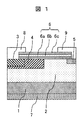
図1は、本発明の一実施例であるSiC半導体装置のターミネーション領域の縦方向断面図を示す。本実施例のターミネーション構造は、高耐圧ダイオードや高耐圧MOSFETなどのパワーデバイスに適用できる。 FIG. 1 is a longitudinal sectional view of a termination region of a SiC semiconductor device according to an embodiment of the present invention. The termination structure of the present embodiment can be applied to power devices such as high voltage diodes and high voltage MOSFETs.
図1に示すように、n+型基板1上に、n+型基板1と接するn−型ドリフト層2が設けられる。n+型基板1とn−型ドリフト層2はn+n−接合を構成する。ここで、n−型ドリフト層2はエピタキシャル成長法などにより形成される。n−型ドリフト層2の上表面部には、n−型ドリフト層2と接するp型JTE領域4と、p型JTE領域4よりも浅く且つp型JTE領域4に接するp+型ガードリング領域3が設けられる。また、n−型ドリフト層2の上表面部にはn+型フィールドストップ領域5が設けられる。p型JTE領域4およびn+型フィールドストップ領域5は、n−型ドリフト層2と、それぞれpn−接合およびn+n−接合を構成する。n−型ドリフト層2の上表面部において、p型JTE領とn+型フィールドストップ領域5の間にはn−型ドリフト層2が介在する。すなわち、p型JTE領域4とn+型フィールドストップ領域5は、接することなく、分かれている。パッシベーション膜などについては、後述する。
As shown in FIG. 1, on the n + -
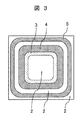
図3は、本実施例の半導体装置の平面図を示す。本図では、n−型ドリフト層2,p+型ガードリング領域3,p型JTE領域4およびn+型フィールドストップ領域5の平面パターンを示しており、パッシベーション膜や電極などは図示を省略している。p+型ガードリング領域3,p型JTE領域4およびn+型フィールドストップ領域5の平面形状は、各々一重の環状である。また、半導体装置の中央部は、ダイオードやMOSFETなどのパワーデバイスのアクティブ領域であるが、本図では、これらの詳細な構成は図示を省略し、簡単のためn−型ドリフト層2だけを示す。図3に示すように、p+型ガードリング領域3、p型JTE領域4およびn+型フィールドストップ領域5は、半導体装置におけるn−型ドリフト層2の中央部に位置するアクティブ領域を囲むように、n−型ドリフト層2の中央部から端部に向かってこの順に配置される。半導体装置の半導体チップにおいて、アクティブ領域の周囲に位置し、これらp+型ガードリング領域3,p型JTE領域4およびn+型フィールドストップ領域5を含む領域が、ターミネーション領域を構成する。アクティブ領域は主電流を制御し、ターミネーション領域は電界を緩和する。
FIG. 3 is a plan view of the semiconductor device of this example. In this figure, the plane pattern of the n −
図1の実施例では、p+型ガードリング領域3およびp型JTE領域4は、SiCからなるn−型ドリフト層2の上表面部にp型の不純物(例えばアルミニウム(Al))をイオン注入によって導入して形成される半導体領域である。本実施例では、p+型ガードリング領域3の方がp型JTE領域4よりも、p型不純物の濃度が高く、かつ不純物の導入深さが浅い。しかし、不純物の濃度および導入深さの大小関係はこれに限らず、等しい場合を含め、任意で良い。n+型フィールドストップ領域5は、半導体装置にかかる電界が半導体装置の半導体チップ端に到達することを防ぐための半導体領域であり、n−型ドリフト層2の上表面部にn型の不純物(例えばリン(P))をイオン注入によって導入して形成される半導体領域である。
In the embodiment of FIG. 1, the p + -type
図1に示すように、n+型基板1の裏面には、n+型基板1と電気的に接触する主電極となる裏面電極7が設けられ、n−型ドリフト層2の上面において、p+型ガードリング領域3と電気的に接触する主電極となる表面電極8が設けられる。また、n−型ドリフト層2の上面において、n−型ドリフト層2の上表面部に電気的に接触するフローティング電極9が設けられる。フローティング電極9は、裏面電極7および表面電極8とは分かれており、本実施例においては外部電極や外部回路とは接続されず、フローティング電位状態にある。裏面電極7,表面電極8およびフローティング電極9は、アルミニウム(Al)などの導体からなる。なお、フローティング電極9は、n+型フィールドストップ領域5の電位を均等化し、n+型フィールドストップ領域5のフィールドストップ動作の信頼性を向上する。
As shown in FIG. 1, on the back surface of the n + -
さらに、図1に示すように、パッシベーション膜6は、n−型ドリフト層2の上面において、裏面電極8とフローティング電極9の間に位置する。裏面電極8とフローティング電極9の各一部は、パッシベーション膜6の表面上に乗り上げるように設けられている。また、パッシべーション膜6は、p+型ガードリング領域3の端部の表面上,p型JTE領域4の表面上,p型JTE領域4とn+型フィールドストップ領域5の間に介在するn−型ドリフト層2の表面上およびn+型フィールドストップ領域5の端部の表面上に跨って、これら表面上を覆うように設けられる。すなわち、本実施例において、パッシべーション膜6は、p+型ガードリング領域3の一部の直上からn+型フィールドストップ領域5の一部の直上にかけて設けられ、ターミネーション領域におけるp型JTE領域4の表面全体、およびp型JTE領域4とn+型フィールドストップ領域5の間に介在するn−型ドリフト層2の表面全体を覆っている。
Further, as shown in FIG. 1, the
パッシべーション膜6は、n−型ドリフト層2の上表面から上方に向かって順に積層される熱酸化シリコン膜6a,LPCVD(Low Pressure Chemical Vapor Deposition)やPECVD(Plasma Enhanced Chemical Vapor Deposition)により堆積形成し焼きしめ処理される酸化シリコン膜6b、およびLPCVDやPECVDにより堆積形成される酸化シリコン膜6cにより構成される。すなわち、パッシベーション膜6において、一層目の熱酸化シリコン膜6aは、p+型ガードリング領域3の端部の表面,p型JTE領域4の表面,p型JTE領域4とn+型フィールドストップ領域5の間に介在するn−型ドリフト層2の表面およびn+型フィールドストップ領域5の端部の表面に接触し、二層目のCVD酸化シリコン膜6bは、熱酸化シリコン膜6aの表面に接触するように積層されると共にCVD酸化シリコン膜6cの全表面を覆い、三相目のCVD酸化シリコン膜6cは、CVD酸化シリコン膜6bの表面に接触するように積層されると共にCVD酸化シリコン膜6bの全表面を覆う。
The
図1に示す実施例におけるパッシベーション膜6は、酸化シリコンからなる無機質の膜を三層のみを有するが、さらにパッシベーション膜6上を、ポリイミド樹脂やポリアミド樹脂などの樹脂からなる保護膜で被覆しても良い。
The
パッシベーション膜6における熱酸化シリコン膜6aとしては、半導体SiC表面のイオン注入のダメージを除去するための犠牲酸化工程において形成される熱酸化膜すなわち犠牲酸化膜の一部が、除去されずに用いられる。従って、パッシベーション膜形成のために熱酸化工程を追加することなく、熱酸化シリコン膜6aを設けることができる。このため、生産コストを増やすことなく、安定した耐圧が得られると共にリーク電流の少ないターミネーション構造を得ることができる。なお、本実施例において、イオン注入は、p+型ガードリング領域3,p型JTE領域4およびn+型フィールドストップ領域5を形成するために用いられる。
As the thermal
本実施例のSiC半導体装置の動作時であって、裏面電極7と表面電極8との間に電圧が印加されるブロッキング状態においては、裏面電極7から表面電極8に向かって電気力線が伸びる。本実施例においては、p+型ガードリング領域3およびp型JTE領域4によって電気力線が横方向に広げられるため、p+型ガードリング領域3に接する表面電極8のエッジ部分における電界集中を緩和できる。この時、パッシベーション膜6に高電界が印加されたとしても、パッシベーション膜6は緻密な膜質順に3層すなわち複数層の酸化シリコン膜からなるため、パッシベーション膜内におけるトラップが生じ難い。このため、リーク電流の増加やパッシベーション膜の破壊が抑制できる。
When the SiC semiconductor device of this embodiment is in operation and in a blocking state in which a voltage is applied between the
上述したように、本実施例によれば、パッシベーション膜が三層の酸化シリコン膜からなるため、パッシベーション膜にかかる電界が緩和されると共に、特別な工程や材料を要することなくパッシベーション膜を設けることができるので、生産コストが低減できる。 As described above, according to this embodiment, since the passivation film is formed of the three-layered silicon oxide film, the electric field applied to the passivation film is alleviated, and the passivation film is provided without requiring a special process or material. Production costs can be reduced.
また、半導体SiC表面上に、熱酸化シリコン膜が設けられ、さらにCVD酸化膜が二層すなわち複数層積層されるので、半導体表面、特に低濃度のn−型ドリフト層2の表面が安定化すると共に、パッシベーション膜の厚さを容易に厚くすることができる。これにより、SiC半導体装置を高耐圧化できると共に、耐圧が安定化し信頼性が向上する。
In addition, since a thermal silicon oxide film is provided on the surface of the semiconductor SiC and two or more layers of CVD oxide films are stacked, the surface of the semiconductor, particularly the surface of the low concentration n −
さらに、上述したように、次のような製造工程によってパッシベーション膜6が形成される。
Furthermore, as described above, the
(a)熱酸化によって半導体表面に犠牲酸化膜を形成する工程。(b)工程aで形成される犠牲酸化膜によって半導体装置のターミネーション領域上にパッシベーション用の熱酸化シリコン膜を形成する工程。(c)工程bで形成されるパッシベーション用の熱酸化シリコン膜上にCVDにより酸化シリコン膜を形成する工程。(d)工程cで形成される酸化シリコン膜上にCVDにより酸化シリコン膜を形成する工程。 (A) A step of forming a sacrificial oxide film on the semiconductor surface by thermal oxidation. (B) A step of forming a thermal silicon oxide film for passivation on the termination region of the semiconductor device by the sacrificial oxide film formed in step a. (C) A step of forming a silicon oxide film by CVD on the thermal oxide silicon film for passivation formed in step b. (D) A step of forming a silicon oxide film by CVD on the silicon oxide film formed in step c.
このように、パッシベーション用の熱酸化膜形成のために熱酸化工程を追加することなく、かつ特別な工程や材料を要することなくパッシベーション膜を設けることができるので、生産コストが低減できる。 As described above, since the passivation film can be provided without adding a thermal oxidation process for forming a thermal oxide film for passivation and without requiring a special process or material, the production cost can be reduced.
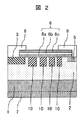
図2は、本発明の他の実施例であるSiC半導体装置のターミネーション領域の縦方向断面図を示す。以下、主に実施例1と異なる点について説明する。 FIG. 2 is a longitudinal sectional view of a termination region of an SiC semiconductor device according to another embodiment of the present invention. Hereinafter, differences from the first embodiment will be mainly described.
本実施例においては、実施例1と異なり、ターミネーション領域がFLR構造を有する。図2に示すように、p+型ガードリング領域3とn+型フィールドストップ領域5の間におけるn−型ドリフト層2の上表面部に、4個のp型FLR領域10が設けられる。p+型ガードリング領域3とこれに近接するp型FLR領域10の間、互いに近接する2個のp型FLR領域10の間、並びにn+型フィールドストップ領域5とこれに近接するp型FLR領域10の間には、n−型ドリフト層2の一部が介在する。すなわち、p+型ガードリング領域3,4個のp型FLR領域10およびn+型フィールドストップ領域5は、互いに分かれている。なお、p型FLR領域10の個数は、所望の耐圧に応じて任意の個数に設定できる。
In this example, unlike Example 1, the termination region has an FLR structure. As shown in FIG. 2, four p-
本実施例の平面パターンは、図3において、p+型ガードリング領域3とn+型フィールドストップ領域5の間のターミネーション領域に、p型JTE領域4に替えて、アクティブ領域を囲むように4重の環状のp型FLR領域10が設けられる。
In FIG. 3, the planar pattern of this embodiment is such that the termination region between the p + type
図2に示すように、パッシベーション膜6は、実施例1と同様に、熱酸化シリコン膜6aおよび熱酸化シリコン膜6a上に順次積層される二層のCVD酸化シリコン膜6b,6cからなる。このようなパッシベーション膜6は、n−型ドリフト層2の上面において、裏面電極8とフローティング電極9の間に位置する。裏面電極8とフローティング電極9の各一部は、パッシベーション膜6の表面上に乗り上げるように設けられている。また、パッシべーション膜6は、p+型ガードリング領域3の端部の表面上,4個のp型FLR領域10の表面上,p+型ガードリング領域3とこれに近接するp型FLR領域10の間に介在するn−型ドリフト層2の表面上,互いに近接する2個のp型FLR領域10の間に介在するn−型ドリフト層2の表面上,n+型フィールドストップ領域5とこれに近接するp型FLR領域10の間に介在するおよびn−型ドリフト層2の表面上,n+型フィールドストップ領域5の端部の表面上に跨って、これら表面上を覆うように設けられる。すなわち、本実施例において、パッシべーション膜6は、p+型ガードリング領域3の一部の直上からn+型フィールドストップ領域5の一部の直上にかけて設けられ、ターミネーション領域における4個のp型FLR領域10の表面全体,p+型ガードリング領域3とこれに近接するp型FLR領域10の間に介在するn−型ドリフト層2の表面全体,互いに近接する2個のp型FLR領域10の間に介在するn−型ドリフト層2の表面全体、およびn+型フィールドストップ領域5とこれに近接するp型FLR領域10の間に介在するn−型ドリフト層2の表面全体を覆っている。
As shown in FIG. 2, the
なお、図2に示す実施例2の他の構成および製造方法は、図1に示す実施例1と同様である。 In addition, the other structure and manufacturing method of Example 2 shown in FIG. 2 are the same as that of Example 1 shown in FIG.
本実施例2によれば、実施例1と同様に、生産コストを増やすことなく、安定した耐圧が得られると共にリーク電流の少ないターミネーション構造を得ることができる。 According to the second embodiment, as in the first embodiment, it is possible to obtain a termination structure with a stable breakdown voltage and a small leakage current without increasing the production cost.
なお、本発明は前述した実施例に限定されるものではなく、様々な変形例が含まれる。例えば、前述した実施例は本発明を分かりやすく説明するために詳細に説明したものであり、必ずしも説明した全ての構成を備えるものに限定されるものではない。また、各実施例の構成の一部について、他の構成の追加・削除・置き換えをすることが可能である。 In addition, this invention is not limited to the Example mentioned above, Various modifications are included. For example, the above-described embodiments have been described in detail for easy understanding of the present invention, and are not necessarily limited to those having all the configurations described. Further, it is possible to add, delete, and replace other configurations for a part of the configuration of each embodiment.
例えば、アクティブ領域に設けられる半導体デバイスとしては、pn接合型ダイオード,ショットキーバリアダイオード,pn接合とショットキーバリアを備える複合型ダイオード,MOSFETやIGBTなどのスイッチングデバイスが適用できる。また、各実施例において、半導体領域の導電型p,nを逆にしても良い。 For example, as a semiconductor device provided in the active region, a pn junction diode, a Schottky barrier diode, a composite diode including a pn junction and a Schottky barrier, a switching device such as a MOSFET or an IGBT can be applied. In each embodiment, the conductivity types p and n of the semiconductor region may be reversed.
1 n+型基板
2 n−型ドリフト層
3 p+型ガードリング領域
4 p型JTE領域
5 n+型フィールドストップ領域
6 パッシベーション膜
6a 熱酸化シリコン膜
6b CVD酸化シリコン膜
6c CVD酸化シリコン膜
7 裏面電極
8 表面電極
9 フローティング電極
10 p型FLR領域
1 n + type substrate 2 n − type drift layer 3 p + type guard ring region 4 p type JTE region 5 n + type
Claims (7)
前記パッシベーション膜は、
前記ターミネーション領域の表面に接する第1酸化シリコン膜と、
前記第1酸化シリコン膜上に積層され、前記第1酸化シリコン膜に接する第2酸化シリコン膜と、
前記第2酸化シリコン膜上に積層され、前記第2酸化シリコン膜に接する第3酸化シリコン膜と、
を備えることを特徴とする半導体装置。 In a semiconductor device made of semiconductor SiC, having a termination region around an active region, and the surface of the termination region being covered with a passivation film,
The passivation film is
A first silicon oxide film in contact with the surface of the termination region;
A second silicon oxide film stacked on the first silicon oxide film and in contact with the first silicon oxide film;
A third silicon oxide film stacked on the second silicon oxide film and in contact with the second silicon oxide film;
A semiconductor device comprising:
熱酸化によって半導体表面に犠牲酸化膜を形成する第1工程と、
前記第1工程で形成される前記犠牲酸化膜によって前記ターミネーション領域上に、前記パッシベーション膜を構成する第1酸化シリコン膜を形成する第2工程と、
前記第2工程で形成される前記第1酸化シリコン膜上に、CVDにより、前記パッシベーション膜を構成する第2酸化シリコン膜を形成する第3工程と、
前記第3工程で形成される前記第2酸化シリコン膜上に、CVDにより、前記パッシベーション膜を構成する第3酸化シリコン膜を形成する第3工程と、
を含むことを特徴とする半導体装置の製造方法。 In a manufacturing method of a semiconductor device, which is made of semiconductor SiC, has a termination region around an active region, and a surface of the termination region is covered with a passivation film.
A first step of forming a sacrificial oxide film on the semiconductor surface by thermal oxidation;
A second step of forming a first silicon oxide film constituting the passivation film on the termination region by the sacrificial oxide film formed in the first step;
A third step of forming a second silicon oxide film constituting the passivation film by CVD on the first silicon oxide film formed in the second step;
Forming a third silicon oxide film constituting the passivation film by CVD on the second silicon oxide film formed in the third process;
A method for manufacturing a semiconductor device, comprising:
Priority Applications (3)
| Application Number | Priority Date | Filing Date | Title |
|---|---|---|---|
| JP2014209618A JP2016081981A (en) | 2014-10-14 | 2014-10-14 | Semiconductor device and manufacturing method of the same |
| US14/878,711 US20160104614A1 (en) | 2014-10-14 | 2015-10-08 | Semiconductor Device and a Method of Manufacturing Same |
| EP15189734.5A EP3010045A1 (en) | 2014-10-14 | 2015-10-14 | Semiconductor device and a method of manufacturing same |
Applications Claiming Priority (1)
| Application Number | Priority Date | Filing Date | Title |
|---|---|---|---|
| JP2014209618A JP2016081981A (en) | 2014-10-14 | 2014-10-14 | Semiconductor device and manufacturing method of the same |
Publications (2)
| Publication Number | Publication Date |
|---|---|
| JP2016081981A true JP2016081981A (en) | 2016-05-16 |
| JP2016081981A5 JP2016081981A5 (en) | 2017-03-09 |
Family
ID=54329411
Family Applications (1)
| Application Number | Title | Priority Date | Filing Date |
|---|---|---|---|
| JP2014209618A Pending JP2016081981A (en) | 2014-10-14 | 2014-10-14 | Semiconductor device and manufacturing method of the same |
Country Status (3)
| Country | Link |
|---|---|
| US (1) | US20160104614A1 (en) |
| EP (1) | EP3010045A1 (en) |
| JP (1) | JP2016081981A (en) |
Families Citing this family (2)
| Publication number | Priority date | Publication date | Assignee | Title |
|---|---|---|---|---|
| JP6547844B2 (en) | 2015-12-18 | 2019-07-24 | 富士電機株式会社 | Silicon carbide semiconductor substrate, method of manufacturing silicon carbide semiconductor substrate, semiconductor device, and method of manufacturing semiconductor device |
| US9998109B1 (en) * | 2017-05-15 | 2018-06-12 | Cree, Inc. | Power module with improved reliability |
Citations (7)
| Publication number | Priority date | Publication date | Assignee | Title |
|---|---|---|---|---|
| JPH07249770A (en) * | 1994-03-10 | 1995-09-26 | Toshiba Corp | Semiconductor device and its fabrication |
| JPH11103070A (en) * | 1997-08-01 | 1999-04-13 | Sony Corp | Thin film transistor |
| JP2010161241A (en) * | 2009-01-08 | 2010-07-22 | Toyota Motor Corp | Semiconductor device and manufacturing method therefor |
| JP2010267783A (en) * | 2009-05-14 | 2010-11-25 | Mitsubishi Electric Corp | Method of manufacturing silicon carbide semiconductor device |
| JP2011040431A (en) * | 2009-08-06 | 2011-02-24 | Panasonic Corp | Semiconductor device and method of manufacturing the same |
| JP2011060939A (en) * | 2009-09-09 | 2011-03-24 | Toshiba Corp | Method of manufacturing semiconductor device |
| WO2013084620A1 (en) * | 2011-12-07 | 2013-06-13 | 住友電気工業株式会社 | Method for manufacturing semiconductor device |
Family Cites Families (9)
| Publication number | Priority date | Publication date | Assignee | Title |
|---|---|---|---|---|
| JPH11330496A (en) | 1998-05-07 | 1999-11-30 | Hitachi Ltd | Semiconductor device |
| US7625603B2 (en) * | 2003-11-14 | 2009-12-01 | Robert Bosch Gmbh | Crack and residue free conformal deposited silicon oxide with predictable and uniform etching characteristics |
| US7598576B2 (en) * | 2005-06-29 | 2009-10-06 | Cree, Inc. | Environmentally robust passivation structures for high-voltage silicon carbide semiconductor devices |
| JP4189415B2 (en) * | 2006-06-30 | 2008-12-03 | 株式会社東芝 | Semiconductor device |
| KR101190942B1 (en) * | 2008-02-12 | 2012-10-12 | 미쓰비시덴키 가부시키가이샤 | Silicon carbide semiconductor device |
| IT1392577B1 (en) * | 2008-12-30 | 2012-03-09 | St Microelectronics Rousset | PROCESS OF MANUFACTURE OF AN ELECTRONIC POWER DEVICE INTEGRATED IN A SEMICONDUCTOR SUBSTRATE WITH A BROADBAND INTERVAL OF PROHIBITED BAND AND ELECTRONIC DEVICE SO IT IS OBTAINED |
| JP5439215B2 (en) * | 2010-02-10 | 2014-03-12 | 株式会社東芝 | Semiconductor device and manufacturing method of semiconductor device |
| JP5628765B2 (en) | 2011-08-19 | 2014-11-19 | 株式会社日立製作所 | Semiconductor device |
| US9991399B2 (en) * | 2012-10-04 | 2018-06-05 | Cree, Inc. | Passivation structure for semiconductor devices |
-
2014
- 2014-10-14 JP JP2014209618A patent/JP2016081981A/en active Pending
-
2015
- 2015-10-08 US US14/878,711 patent/US20160104614A1/en not_active Abandoned
- 2015-10-14 EP EP15189734.5A patent/EP3010045A1/en not_active Withdrawn
Patent Citations (7)
| Publication number | Priority date | Publication date | Assignee | Title |
|---|---|---|---|---|
| JPH07249770A (en) * | 1994-03-10 | 1995-09-26 | Toshiba Corp | Semiconductor device and its fabrication |
| JPH11103070A (en) * | 1997-08-01 | 1999-04-13 | Sony Corp | Thin film transistor |
| JP2010161241A (en) * | 2009-01-08 | 2010-07-22 | Toyota Motor Corp | Semiconductor device and manufacturing method therefor |
| JP2010267783A (en) * | 2009-05-14 | 2010-11-25 | Mitsubishi Electric Corp | Method of manufacturing silicon carbide semiconductor device |
| JP2011040431A (en) * | 2009-08-06 | 2011-02-24 | Panasonic Corp | Semiconductor device and method of manufacturing the same |
| JP2011060939A (en) * | 2009-09-09 | 2011-03-24 | Toshiba Corp | Method of manufacturing semiconductor device |
| WO2013084620A1 (en) * | 2011-12-07 | 2013-06-13 | 住友電気工業株式会社 | Method for manufacturing semiconductor device |
Also Published As
| Publication number | Publication date |
|---|---|
| EP3010045A1 (en) | 2016-04-20 |
| US20160104614A1 (en) | 2016-04-14 |
Similar Documents
| Publication | Publication Date | Title |
|---|---|---|
| US10090417B2 (en) | Silicon carbide semiconductor device and fabrication method of silicon carbide semiconductor device | |
| JP2015118966A (en) | Semiconductor device | |
| JP6833848B2 (en) | Area-efficient floating field ring termination | |
| JP6519455B2 (en) | Semiconductor device | |
| JP5628765B2 (en) | Semiconductor device | |
| WO2016013472A1 (en) | Semiconductor device and method for manufacturing semiconductor device | |
| JP2015185751A (en) | insulated gate semiconductor device | |
| JP2014120685A (en) | Semiconductor device | |
| JP6363540B2 (en) | Semiconductor device | |
| JP6847007B2 (en) | Semiconductor devices and their manufacturing methods | |
| JP5888214B2 (en) | Nitride-based compound semiconductor device and manufacturing method thereof | |
| WO2017159034A1 (en) | Semiconductor device | |
| JP2016035989A (en) | Semiconductor device | |
| WO2012124191A1 (en) | Semiconductor device | |
| JP6592083B2 (en) | Semiconductor device, manufacturing method thereof, and power module | |
| JP2013182905A (en) | Semiconductor device | |
| JP2016081981A (en) | Semiconductor device and manufacturing method of the same | |
| JP6589278B2 (en) | Semiconductor device and method for manufacturing semiconductor device | |
| JP7159949B2 (en) | semiconductor equipment | |
| JP2012004466A (en) | Semiconductor device | |
| JP2017092364A (en) | Semiconductor device and semiconductor device manufacturing method | |
| JP5938242B2 (en) | diode | |
| JP6609283B2 (en) | Silicon carbide semiconductor device | |
| JP2015084444A (en) | Semiconductor device | |
| JP2016162783A (en) | Semiconductor device |
Legal Events
| Date | Code | Title | Description |
|---|---|---|---|
| A521 | Request for written amendment filed |
Free format text: JAPANESE INTERMEDIATE CODE: A523 Effective date: 20170202 |
|
| A621 | Written request for application examination |
Free format text: JAPANESE INTERMEDIATE CODE: A621 Effective date: 20170202 |
|
| A131 | Notification of reasons for refusal |
Free format text: JAPANESE INTERMEDIATE CODE: A131 Effective date: 20170801 |
|
| A521 | Request for written amendment filed |
Free format text: JAPANESE INTERMEDIATE CODE: A523 Effective date: 20170905 |
|
| A131 | Notification of reasons for refusal |
Free format text: JAPANESE INTERMEDIATE CODE: A131 Effective date: 20171031 |
|
| A521 | Request for written amendment filed |
Free format text: JAPANESE INTERMEDIATE CODE: A523 Effective date: 20171205 |
|
| A02 | Decision of refusal |
Free format text: JAPANESE INTERMEDIATE CODE: A02 Effective date: 20180123 |