JP2015204237A - 有機エレクトロルミネッセンス表示装置および有機エレクトロルミネッセンス表示装置の製造方法 - Google Patents
有機エレクトロルミネッセンス表示装置および有機エレクトロルミネッセンス表示装置の製造方法 Download PDFInfo
- Publication number
- JP2015204237A JP2015204237A JP2014083904A JP2014083904A JP2015204237A JP 2015204237 A JP2015204237 A JP 2015204237A JP 2014083904 A JP2014083904 A JP 2014083904A JP 2014083904 A JP2014083904 A JP 2014083904A JP 2015204237 A JP2015204237 A JP 2015204237A
- Authority
- JP
- Japan
- Prior art keywords
- film
- display device
- pixel electrode
- region
- organic electroluminescence
- Prior art date
- Legal status (The legal status is an assumption and is not a legal conclusion. Google has not performed a legal analysis and makes no representation as to the accuracy of the status listed.)
- Pending
Links
- 238000004519 manufacturing process Methods 0.000 title claims abstract description 34
- 239000000758 substrate Substances 0.000 claims abstract description 62
- 238000000926 separation method Methods 0.000 claims abstract description 25
- 239000011159 matrix material Substances 0.000 claims abstract description 7
- 238000005401 electroluminescence Methods 0.000 claims description 70
- 238000007789 sealing Methods 0.000 claims description 41
- 238000000034 method Methods 0.000 claims description 40
- 229910010272 inorganic material Inorganic materials 0.000 claims description 10
- 239000011147 inorganic material Substances 0.000 claims description 10
- 238000002955 isolation Methods 0.000 claims description 9
- 239000011368 organic material Substances 0.000 claims description 8
- 238000005192 partition Methods 0.000 claims description 2
- 238000009413 insulation Methods 0.000 abstract 2
- 239000010408 film Substances 0.000 description 157
- 239000010410 layer Substances 0.000 description 31
- 230000001681 protective effect Effects 0.000 description 23
- 239000000463 material Substances 0.000 description 19
- 239000012044 organic layer Substances 0.000 description 18
- 229920005989 resin Polymers 0.000 description 13
- 239000011347 resin Substances 0.000 description 13
- 239000010409 thin film Substances 0.000 description 12
- 238000007774 anilox coating Methods 0.000 description 4
- 239000003086 colorant Substances 0.000 description 4
- 238000004040 coloring Methods 0.000 description 4
- 239000011810 insulating material Substances 0.000 description 4
- 229910052751 metal Inorganic materials 0.000 description 4
- 239000002184 metal Substances 0.000 description 4
- 229910052709 silver Inorganic materials 0.000 description 3
- 239000004332 silver Substances 0.000 description 3
- FYYHWMGAXLPEAU-UHFFFAOYSA-N Magnesium Chemical compound [Mg] FYYHWMGAXLPEAU-UHFFFAOYSA-N 0.000 description 2
- XLOMVQKBTHCTTD-UHFFFAOYSA-N Zinc monoxide Chemical compound [Zn]=O XLOMVQKBTHCTTD-UHFFFAOYSA-N 0.000 description 2
- 239000002131 composite material Substances 0.000 description 2
- 239000000945 filler Substances 0.000 description 2
- 238000002347 injection Methods 0.000 description 2
- 239000007924 injection Substances 0.000 description 2
- 230000001678 irradiating effect Effects 0.000 description 2
- 229910052749 magnesium Inorganic materials 0.000 description 2
- 239000011777 magnesium Substances 0.000 description 2
- 229910044991 metal oxide Inorganic materials 0.000 description 2
- 150000004706 metal oxides Chemical class 0.000 description 2
- 230000004048 modification Effects 0.000 description 2
- 238000012986 modification Methods 0.000 description 2
- 238000002161 passivation Methods 0.000 description 2
- 239000011342 resin composition Substances 0.000 description 2
- 239000004642 Polyimide Substances 0.000 description 1
- 229910004298 SiO 2 Inorganic materials 0.000 description 1
- NIXOWILDQLNWCW-UHFFFAOYSA-N acrylic acid group Chemical group C(C=C)(=O)O NIXOWILDQLNWCW-UHFFFAOYSA-N 0.000 description 1
- QVGXLLKOCUKJST-UHFFFAOYSA-N atomic oxygen Chemical compound [O] QVGXLLKOCUKJST-UHFFFAOYSA-N 0.000 description 1
- 239000004020 conductor Substances 0.000 description 1
- 238000007796 conventional method Methods 0.000 description 1
- 238000001723 curing Methods 0.000 description 1
- 230000006866 deterioration Effects 0.000 description 1
- 230000000694 effects Effects 0.000 description 1
- 238000009429 electrical wiring Methods 0.000 description 1
- 230000005525 hole transport Effects 0.000 description 1
- 229910003437 indium oxide Inorganic materials 0.000 description 1
- NJWNEWQMQCGRDO-UHFFFAOYSA-N indium zinc Chemical compound [Zn].[In] NJWNEWQMQCGRDO-UHFFFAOYSA-N 0.000 description 1
- PJXISJQVUVHSOJ-UHFFFAOYSA-N indium(iii) oxide Chemical compound [O-2].[O-2].[O-2].[In+3].[In+3] PJXISJQVUVHSOJ-UHFFFAOYSA-N 0.000 description 1
- AMGQUBHHOARCQH-UHFFFAOYSA-N indium;oxotin Chemical compound [In].[Sn]=O AMGQUBHHOARCQH-UHFFFAOYSA-N 0.000 description 1
- 238000009434 installation Methods 0.000 description 1
- 238000010030 laminating Methods 0.000 description 1
- 239000012528 membrane Substances 0.000 description 1
- 238000002156 mixing Methods 0.000 description 1
- TWNQGVIAIRXVLR-UHFFFAOYSA-N oxo(oxoalumanyloxy)alumane Chemical compound O=[Al]O[Al]=O TWNQGVIAIRXVLR-UHFFFAOYSA-N 0.000 description 1
- 229910052760 oxygen Inorganic materials 0.000 description 1
- 239000001301 oxygen Substances 0.000 description 1
- 238000000016 photochemical curing Methods 0.000 description 1
- 239000000049 pigment Substances 0.000 description 1
- 229910021420 polycrystalline silicon Inorganic materials 0.000 description 1
- 229920001721 polyimide Polymers 0.000 description 1
- 229920005591 polysilicon Polymers 0.000 description 1
- 230000002265 prevention Effects 0.000 description 1
- 239000004065 semiconductor Substances 0.000 description 1
- 238000004904 shortening Methods 0.000 description 1
- 238000000638 solvent extraction Methods 0.000 description 1
- 230000001629 suppression Effects 0.000 description 1
- XOLBLPGZBRYERU-UHFFFAOYSA-N tin dioxide Chemical compound O=[Sn]=O XOLBLPGZBRYERU-UHFFFAOYSA-N 0.000 description 1
- 229910001887 tin oxide Inorganic materials 0.000 description 1
- 239000012780 transparent material Substances 0.000 description 1
- 239000011787 zinc oxide Substances 0.000 description 1
Images


Classifications
-
- H—ELECTRICITY
- H10—SEMICONDUCTOR DEVICES; ELECTRIC SOLID-STATE DEVICES NOT OTHERWISE PROVIDED FOR
- H10K—ORGANIC ELECTRIC SOLID-STATE DEVICES
- H10K59/00—Integrated devices, or assemblies of multiple devices, comprising at least one organic light-emitting element covered by group H10K50/00
- H10K59/30—Devices specially adapted for multicolour light emission
- H10K59/38—Devices specially adapted for multicolour light emission comprising colour filters or colour changing media [CCM]
-
- H—ELECTRICITY
- H10—SEMICONDUCTOR DEVICES; ELECTRIC SOLID-STATE DEVICES NOT OTHERWISE PROVIDED FOR
- H10K—ORGANIC ELECTRIC SOLID-STATE DEVICES
- H10K59/00—Integrated devices, or assemblies of multiple devices, comprising at least one organic light-emitting element covered by group H10K50/00
- H10K59/80—Constructional details
- H10K59/87—Passivation; Containers; Encapsulations
- H10K59/873—Encapsulations
-
- H—ELECTRICITY
- H10—SEMICONDUCTOR DEVICES; ELECTRIC SOLID-STATE DEVICES NOT OTHERWISE PROVIDED FOR
- H10K—ORGANIC ELECTRIC SOLID-STATE DEVICES
- H10K2102/00—Constructional details relating to the organic devices covered by this subclass
- H10K2102/301—Details of OLEDs
- H10K2102/302—Details of OLEDs of OLED structures
- H10K2102/3023—Direction of light emission
- H10K2102/3026—Top emission
-
- H—ELECTRICITY
- H10—SEMICONDUCTOR DEVICES; ELECTRIC SOLID-STATE DEVICES NOT OTHERWISE PROVIDED FOR
- H10K—ORGANIC ELECTRIC SOLID-STATE DEVICES
- H10K50/00—Organic light-emitting devices
- H10K50/80—Constructional details
- H10K50/84—Passivation; Containers; Encapsulations
- H10K50/844—Encapsulations
-
- H—ELECTRICITY
- H10—SEMICONDUCTOR DEVICES; ELECTRIC SOLID-STATE DEVICES NOT OTHERWISE PROVIDED FOR
- H10K—ORGANIC ELECTRIC SOLID-STATE DEVICES
- H10K59/00—Integrated devices, or assemblies of multiple devices, comprising at least one organic light-emitting element covered by group H10K50/00
- H10K59/10—OLED displays
- H10K59/12—Active-matrix OLED [AMOLED] displays
- H10K59/122—Pixel-defining structures or layers, e.g. banks
Abstract
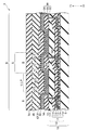
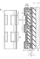
【解決手段】本発明の有機エレクトロルミネッセンス表示装置1の製造方法は、複数の画素Pがマトリクス状に配置されたTFT基板10と、前記TFT基板上に形成された画素電極32と、前記画素電極上に、隣接する前記画素同士の間を区分するように設けられた、前記画素電極の一部を露出させる画素分離膜14と、露出した前記画素電極上を覆う発光層33と、前記発光層上と前記画素分離膜上を覆う対向電極34と、前記対向電極上において、露出した前記画素電極に対応する領域である凹領域と前記画素分離膜上の領域である凸領域とを覆う封止絶縁膜40と、前記封止絶縁膜の前記凹領域を埋め込むように形成された着色膜R,G,Bと、を備えることを特徴とする。
【選択図】図3
Description
を備えることを特徴とする。
Claims (6)
- 複数の画素がマトリクス状に配置されたTFT基板と、
前記TFT基板上に形成された画素電極と、
前記画素電極上に、隣接する前記画素同士の間を区分するように設けられた、前記画素電極の一部を露出させる画素分離膜と、
露出した前記画素電極上を覆う発光層と、
前記発光層上と前記画素分離膜上を覆う対向電極と、
前記対向電極上において、露出した前記画素電極に対応する領域である凹領域と前記画素分離膜上の領域である凸領域とを覆う封止絶縁膜と、
前記封止絶縁膜の前記凹領域を埋め込むように形成された着色膜と、
を備えることを特徴とする有機エレクトロルミネッセンス表示装置。 - 請求項1に記載の有機エレクトロルミネッセンス表示装置であって、
前記封止絶縁膜が無機材料からなることを特徴とする有機エレクトロルミネッセンス表示装置。 - 請求項1に記載の有機エレクトロルミネッセンス表示装置であって、
前記封止絶縁膜が有機材料からなる膜と無機材料からなる膜の多層構造であることを特徴とする有機エレクトロルミネッセンス表示装置。 - 複数の画素がマトリクス状に配置されたTFT基板上に画素電極を形成する工程と、
前記画素電極上に、前記画素電極の一部を露出するように、隣接する前記画素同士の間を区分する画素分離膜を形成する工程と、
露出した前記画素電極上を覆うように発光層を形成する工程と、
前記発光層上と前記画素分離膜上を覆うように対向電極を形成する工程と、
前記対向電極上に、露出した前記画素電極に対応する領域である凹領域と前記画素分離膜上の領域である凸領域とを覆うように封止絶縁膜を形成する工程と、
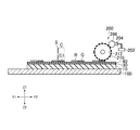
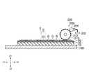
前記封止絶縁膜の前記凹領域を埋め込むように着色膜を形成する工程と、
を備えることを特徴とする有機エレクトロルミネッセンス表示装置の製造方法。 - 請求項4に記載の有機エレクトロルミネッセンス表示装置の製造方法であって、
前記着色膜を、印刷法により前記凹領域に埋め込むことを特徴とする有機エレクトロルミネッセンス表示装置の製造方法。 - 請求項5に記載の有機エレクトロルミネッセンス表示装置の製造方法であって、
前記印刷法が、フレキソ印刷法であることを特徴とする有機エレクトロルミネッセンス表示装置の製造方法。
Priority Applications (4)
| Application Number | Priority Date | Filing Date | Title |
|---|---|---|---|
| JP2014083904A JP2015204237A (ja) | 2014-04-15 | 2014-04-15 | 有機エレクトロルミネッセンス表示装置および有機エレクトロルミネッセンス表示装置の製造方法 |
| KR1020150051627A KR20150118912A (ko) | 2014-04-15 | 2015-04-13 | 표시 장치 및 표시 장치의 제조 방법 |
| US14/686,314 US20150295013A1 (en) | 2014-04-15 | 2015-04-14 | Display device and manufacturing method for display device |
| CN201510178439.8A CN105047684A (zh) | 2014-04-15 | 2015-04-15 | 显示装置和显示装置的制造方法 |
Applications Claiming Priority (1)
| Application Number | Priority Date | Filing Date | Title |
|---|---|---|---|
| JP2014083904A JP2015204237A (ja) | 2014-04-15 | 2014-04-15 | 有機エレクトロルミネッセンス表示装置および有機エレクトロルミネッセンス表示装置の製造方法 |
Publications (2)
| Publication Number | Publication Date |
|---|---|
| JP2015204237A true JP2015204237A (ja) | 2015-11-16 |
| JP2015204237A5 JP2015204237A5 (ja) | 2017-05-25 |
Family
ID=54265737
Family Applications (1)
| Application Number | Title | Priority Date | Filing Date |
|---|---|---|---|
| JP2014083904A Pending JP2015204237A (ja) | 2014-04-15 | 2014-04-15 | 有機エレクトロルミネッセンス表示装置および有機エレクトロルミネッセンス表示装置の製造方法 |
Country Status (4)
| Country | Link |
|---|---|
| US (1) | US20150295013A1 (ja) |
| JP (1) | JP2015204237A (ja) |
| KR (1) | KR20150118912A (ja) |
| CN (1) | CN105047684A (ja) |
Families Citing this family (9)
| Publication number | Priority date | Publication date | Assignee | Title |
|---|---|---|---|---|
| JP6486848B2 (ja) * | 2016-02-25 | 2019-03-20 | 株式会社ジャパンディスプレイ | 表示装置およびその製造方法 |
| US9941330B2 (en) | 2016-05-18 | 2018-04-10 | Globalfoundries Inc. | LEDs with three color RGB pixels for displays |
| US10388691B2 (en) | 2016-05-18 | 2019-08-20 | Globalfoundries Inc. | Light emitting diodes (LEDs) with stacked multi-color pixels for displays |
| US9941329B2 (en) * | 2016-05-18 | 2018-04-10 | Globalfoundries Inc. | Light emitting diodes (LEDs) with integrated CMOS circuits |
| US10037981B2 (en) | 2016-05-18 | 2018-07-31 | Globalfoundries Inc. | Integrated display system with multi-color light emitting diodes (LEDs) |
| KR102590011B1 (ko) * | 2016-08-31 | 2023-10-16 | 엘지디스플레이 주식회사 | 유기 발광 표시 장치 및 이의 제조 방법 |
| WO2018158953A1 (ja) * | 2017-03-03 | 2018-09-07 | シャープ株式会社 | 表示装置およびその製造方法 |
| CN109841661A (zh) * | 2019-02-20 | 2019-06-04 | 武汉华星光电半导体显示技术有限公司 | 显示器及其制备方法 |
| CN113380862B (zh) * | 2021-05-31 | 2023-12-22 | 合肥维信诺科技有限公司 | 显示面板及其制备方法 |
Citations (5)
| Publication number | Priority date | Publication date | Assignee | Title |
|---|---|---|---|---|
| WO2004055763A1 (ja) * | 2002-12-13 | 2004-07-01 | Semiconductor Energy Laboratory Co.,Ltd. | 発光装置及び電子機器 |
| WO2004059600A1 (ja) * | 2002-12-26 | 2004-07-15 | Semiconductor Energy Laboratory Co., Ltd. | 発光装置および電子機器 |
| US20100171107A1 (en) * | 2009-01-07 | 2010-07-08 | Samsung Mobile Display Co., Ltd. | Organic light emitting diode display |
| JP2012194313A (ja) * | 2011-03-16 | 2012-10-11 | Toppan Printing Co Ltd | パターンニング基板の開口部におけるインキ平坦固化方法及び平坦固化装置 |
| JP2013251224A (ja) * | 2012-06-04 | 2013-12-12 | Panasonic Corp | 表示パネルの製造方法、その検査装置及び検査方法 |
Family Cites Families (10)
| Publication number | Priority date | Publication date | Assignee | Title |
|---|---|---|---|---|
| US5340619A (en) * | 1993-10-18 | 1994-08-23 | Brewer Science, Inc. | Method of manufacturing a color filter array |
| JP3633591B2 (ja) * | 2001-07-27 | 2005-03-30 | セイコーエプソン株式会社 | 電気光学装置用基板、電気光学装置用基板の製造方法、電気光学装置、電気光学装置の製造方法、及び、電子機器 |
| JP4207602B2 (ja) * | 2003-02-27 | 2009-01-14 | 三菱化学株式会社 | カラー液晶表示装置 |
| KR20050029426A (ko) * | 2003-09-22 | 2005-03-28 | 삼성에스디아이 주식회사 | 칼라필터층 또는 색변환층을 갖는 풀칼라 유기전계발광소자 |
| CN100379050C (zh) * | 2003-10-20 | 2008-04-02 | 友达光电股份有限公司 | 全色化有机电致发光显示器及其制作方法 |
| KR101230308B1 (ko) * | 2006-02-22 | 2013-02-06 | 삼성디스플레이 주식회사 | 표시 장치 |
| JP4809087B2 (ja) * | 2006-03-14 | 2011-11-02 | セイコーエプソン株式会社 | エレクトロルミネッセンス装置、電子機器、およびエレクトロルミネッセンス装置の製造方法 |
| JP2013045635A (ja) * | 2011-08-24 | 2013-03-04 | Sony Corp | 有機el表示装置、有機el表示装置の製造方法および電子機器 |
| KR101980233B1 (ko) * | 2012-09-04 | 2019-05-21 | 삼성디스플레이 주식회사 | 유기 발광 표시 장치 및 그 제조 방법 |
| JP6220300B2 (ja) * | 2014-03-20 | 2017-10-25 | 株式会社ジャパンディスプレイ | 有機エレクトロルミネセンス表示装置の製造方法及び有機エレクトロルミネセンス表示装置 |
-
2014
- 2014-04-15 JP JP2014083904A patent/JP2015204237A/ja active Pending
-
2015
- 2015-04-13 KR KR1020150051627A patent/KR20150118912A/ko active Search and Examination
- 2015-04-14 US US14/686,314 patent/US20150295013A1/en not_active Abandoned
- 2015-04-15 CN CN201510178439.8A patent/CN105047684A/zh active Pending
Patent Citations (5)
| Publication number | Priority date | Publication date | Assignee | Title |
|---|---|---|---|---|
| WO2004055763A1 (ja) * | 2002-12-13 | 2004-07-01 | Semiconductor Energy Laboratory Co.,Ltd. | 発光装置及び電子機器 |
| WO2004059600A1 (ja) * | 2002-12-26 | 2004-07-15 | Semiconductor Energy Laboratory Co., Ltd. | 発光装置および電子機器 |
| US20100171107A1 (en) * | 2009-01-07 | 2010-07-08 | Samsung Mobile Display Co., Ltd. | Organic light emitting diode display |
| JP2012194313A (ja) * | 2011-03-16 | 2012-10-11 | Toppan Printing Co Ltd | パターンニング基板の開口部におけるインキ平坦固化方法及び平坦固化装置 |
| JP2013251224A (ja) * | 2012-06-04 | 2013-12-12 | Panasonic Corp | 表示パネルの製造方法、その検査装置及び検査方法 |
Also Published As
| Publication number | Publication date |
|---|---|
| US20150295013A1 (en) | 2015-10-15 |
| CN105047684A (zh) | 2015-11-11 |
| KR20150118912A (ko) | 2015-10-23 |
Similar Documents
| Publication | Publication Date | Title |
|---|---|---|
| KR101839263B1 (ko) | 유기 전계 발광 표시장치 및 유기 전계 발광 표시장치의 제조방법 | |
| JP2015204237A (ja) | 有機エレクトロルミネッセンス表示装置および有機エレクトロルミネッセンス表示装置の製造方法 | |
| JP6396879B2 (ja) | 表示装置 | |
| JP6114670B2 (ja) | 有機エレクトロルミネッセンス表示装置及び有機エレクトロルミネッセンス表示装置の製造方法 | |
| TWI569438B (zh) | 有機el顯示裝置 | |
| JP6054763B2 (ja) | 有機el表示装置 | |
| JP6087251B2 (ja) | 有機エレクトロルミネッセンス表示装置 | |
| JP6045276B2 (ja) | 有機el表示装置及び有機el表示装置の製造方法 | |
| JP6133173B2 (ja) | 有機エレクトロルミネッセンス表示装置 | |
| JP6399801B2 (ja) | 有機エレクトロルミネッセンス表示装置 | |
| JP2015072764A (ja) | 表示装置及び表示装置の製造方法 | |
| KR102495122B1 (ko) | 표시 장치 | |
| JP2015049947A (ja) | 有機エレクトロルミネッセンス表示装置 | |
| JP6474337B2 (ja) | 表示装置及びその製造方法 | |
| US20190019857A1 (en) | Organic el display device | |
| JP6220171B2 (ja) | 有機エレクトロルミネッセンス表示装置 | |
| JP6444446B2 (ja) | 有機エレクトロルミネッセンス表示装置及び有機エレクトロルミネッセンス表示装置の製造方法 | |
| JP2018022624A (ja) | 表示装置、表示装置の製造方法 | |
| US20150236305A1 (en) | Method for manufacturing organic electroluminescent display device | |
| JP2018037354A (ja) | 表示装置 | |
| JP2013211132A (ja) | 発光デバイス、発光デバイスの製造方法及び電子機器 |
Legal Events
| Date | Code | Title | Description |
|---|---|---|---|
| A521 | Request for written amendment filed |
Free format text: JAPANESE INTERMEDIATE CODE: A523 Effective date: 20170405 |
|
| A621 | Written request for application examination |
Free format text: JAPANESE INTERMEDIATE CODE: A621 Effective date: 20170405 |
|
| A977 | Report on retrieval |
Free format text: JAPANESE INTERMEDIATE CODE: A971007 Effective date: 20180308 |
|
| A131 | Notification of reasons for refusal |
Free format text: JAPANESE INTERMEDIATE CODE: A131 Effective date: 20180403 |
|
| A02 | Decision of refusal |
Free format text: JAPANESE INTERMEDIATE CODE: A02 Effective date: 20181009 |