JP2015018918A - 反射型原版、露光方法及びデバイス製造方法 - Google Patents
反射型原版、露光方法及びデバイス製造方法 Download PDFInfo
- Publication number
- JP2015018918A JP2015018918A JP2013144855A JP2013144855A JP2015018918A JP 2015018918 A JP2015018918 A JP 2015018918A JP 2013144855 A JP2013144855 A JP 2013144855A JP 2013144855 A JP2013144855 A JP 2013144855A JP 2015018918 A JP2015018918 A JP 2015018918A
- Authority
- JP
- Japan
- Prior art keywords
- layer
- reflective
- diffusion layer
- reflective layer
- original plate
- Prior art date
- Legal status (The legal status is an assumption and is not a legal conclusion. Google has not performed a legal analysis and makes no representation as to the accuracy of the status listed.)
- Pending
Links
- 238000000034 method Methods 0.000 title claims description 22
- 238000004519 manufacturing process Methods 0.000 title claims description 13
- 238000009792 diffusion process Methods 0.000 claims abstract description 45
- 239000000758 substrate Substances 0.000 claims abstract description 36
- 239000010410 layer Substances 0.000 claims description 148
- 239000000463 material Substances 0.000 claims description 20
- 239000002356 single layer Substances 0.000 claims description 6
- 239000011241 protective layer Substances 0.000 claims description 3
- 230000001678 irradiating effect Effects 0.000 claims description 2
- 230000006378 damage Effects 0.000 abstract description 6
- 239000002245 particle Substances 0.000 description 36
- 238000004140 cleaning Methods 0.000 description 17
- 238000007689 inspection Methods 0.000 description 13
- 230000003287 optical effect Effects 0.000 description 11
- 238000009826 distribution Methods 0.000 description 10
- 230000008569 process Effects 0.000 description 9
- 230000008859 change Effects 0.000 description 8
- 239000011521 glass Substances 0.000 description 7
- 239000004065 semiconductor Substances 0.000 description 7
- 238000010586 diagram Methods 0.000 description 6
- 230000007423 decrease Effects 0.000 description 5
- 238000013461 design Methods 0.000 description 5
- 229910004298 SiO 2 Inorganic materials 0.000 description 4
- 238000010521 absorption reaction Methods 0.000 description 4
- 230000000630 rising effect Effects 0.000 description 4
- 230000035939 shock Effects 0.000 description 4
- 238000012546 transfer Methods 0.000 description 4
- 238000004364 calculation method Methods 0.000 description 3
- 239000003795 chemical substances by application Substances 0.000 description 3
- 238000005108 dry cleaning Methods 0.000 description 3
- 239000000126 substance Substances 0.000 description 3
- 230000001133 acceleration Effects 0.000 description 2
- 230000009471 action Effects 0.000 description 2
- 230000015572 biosynthetic process Effects 0.000 description 2
- 239000000356 contaminant Substances 0.000 description 2
- 238000001514 detection method Methods 0.000 description 2
- 239000004973 liquid crystal related substance Substances 0.000 description 2
- 230000009467 reduction Effects 0.000 description 2
- 238000002310 reflectometry Methods 0.000 description 2
- 230000035945 sensitivity Effects 0.000 description 2
- 238000000926 separation method Methods 0.000 description 2
- 230000003685 thermal hair damage Effects 0.000 description 2
- 239000012298 atmosphere Substances 0.000 description 1
- 230000005540 biological transmission Effects 0.000 description 1
- 239000004020 conductor Substances 0.000 description 1
- 238000011109 contamination Methods 0.000 description 1
- 238000012937 correction Methods 0.000 description 1
- 238000005538 encapsulation Methods 0.000 description 1
- 238000002474 experimental method Methods 0.000 description 1
- 238000011065 in-situ storage Methods 0.000 description 1
- 230000031700 light absorption Effects 0.000 description 1
- 238000012986 modification Methods 0.000 description 1
- 230000004048 modification Effects 0.000 description 1
- 230000003647 oxidation Effects 0.000 description 1
- 238000007254 oxidation reaction Methods 0.000 description 1
- 238000012858 packaging process Methods 0.000 description 1
- 230000000737 periodic effect Effects 0.000 description 1
- 230000000704 physical effect Effects 0.000 description 1
- 238000012545 processing Methods 0.000 description 1
- 230000001681 protective effect Effects 0.000 description 1
- 238000012827 research and development Methods 0.000 description 1
- 238000004088 simulation Methods 0.000 description 1
- 238000012360 testing method Methods 0.000 description 1
- 239000002470 thermal conductor Substances 0.000 description 1
- 238000002834 transmittance Methods 0.000 description 1
Images


Classifications
-
- G—PHYSICS
- G03—PHOTOGRAPHY; CINEMATOGRAPHY; ANALOGOUS TECHNIQUES USING WAVES OTHER THAN OPTICAL WAVES; ELECTROGRAPHY; HOLOGRAPHY
- G03F—PHOTOMECHANICAL PRODUCTION OF TEXTURED OR PATTERNED SURFACES, e.g. FOR PRINTING, FOR PROCESSING OF SEMICONDUCTOR DEVICES; MATERIALS THEREFOR; ORIGINALS THEREFOR; APPARATUS SPECIALLY ADAPTED THEREFOR
- G03F1/00—Originals for photomechanical production of textured or patterned surfaces, e.g., masks, photo-masks, reticles; Mask blanks or pellicles therefor; Containers specially adapted therefor; Preparation thereof
- G03F1/22—Masks or mask blanks for imaging by radiation of 100nm or shorter wavelength, e.g. X-ray masks, extreme ultraviolet [EUV] masks; Preparation thereof
- G03F1/24—Reflection masks; Preparation thereof
-
- G—PHYSICS
- G03—PHOTOGRAPHY; CINEMATOGRAPHY; ANALOGOUS TECHNIQUES USING WAVES OTHER THAN OPTICAL WAVES; ELECTROGRAPHY; HOLOGRAPHY
- G03F—PHOTOMECHANICAL PRODUCTION OF TEXTURED OR PATTERNED SURFACES, e.g. FOR PRINTING, FOR PROCESSING OF SEMICONDUCTOR DEVICES; MATERIALS THEREFOR; ORIGINALS THEREFOR; APPARATUS SPECIALLY ADAPTED THEREFOR
- G03F1/00—Originals for photomechanical production of textured or patterned surfaces, e.g., masks, photo-masks, reticles; Mask blanks or pellicles therefor; Containers specially adapted therefor; Preparation thereof
- G03F1/22—Masks or mask blanks for imaging by radiation of 100nm or shorter wavelength, e.g. X-ray masks, extreme ultraviolet [EUV] masks; Preparation thereof
-
- G—PHYSICS
- G03—PHOTOGRAPHY; CINEMATOGRAPHY; ANALOGOUS TECHNIQUES USING WAVES OTHER THAN OPTICAL WAVES; ELECTROGRAPHY; HOLOGRAPHY
- G03F—PHOTOMECHANICAL PRODUCTION OF TEXTURED OR PATTERNED SURFACES, e.g. FOR PRINTING, FOR PROCESSING OF SEMICONDUCTOR DEVICES; MATERIALS THEREFOR; ORIGINALS THEREFOR; APPARATUS SPECIALLY ADAPTED THEREFOR
- G03F7/00—Photomechanical, e.g. photolithographic, production of textured or patterned surfaces, e.g. printing surfaces; Materials therefor, e.g. comprising photoresists; Apparatus specially adapted therefor
- G03F7/20—Exposure; Apparatus therefor
- G03F7/2002—Exposure; Apparatus therefor with visible light or UV light, through an original having an opaque pattern on a transparent support, e.g. film printing, projection printing; by reflection of visible or UV light from an original such as a printed image
Abstract
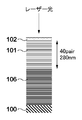
【解決手段】反射型原版は、極端紫外光を反射する多層膜からなる反射層101と、前記反射層を支持する基材100と、前記反射層101と前記基材100との間に設けられ、前記反射層の熱を拡散する熱拡散層104と、を有する。前記反射層101と前記熱拡散層104とで構成する構造体の単位面積当たりの熱容量は、1.1(J/(K・m2))以上である。
【選択図】図1
Description
本発明が適用される極端紫外光(EUV光)を用いて基板を露光するEUV露光装置を図2で説明する。同図で、反射型のレチクル(反射型原版)2には電子回路パターンが形成されている。なお、本発明では、マスクとレチクルは同義語であるとして説明する。特にパターン、多層膜に注目する場合は「マスク」という表現を用い、基板に注目する場合は「レチクル」という表現を用いる。
通常、EUVマスクの膜構造は、EUV光を反射する多層膜(以後、反射層と称す)と、その反射層の表面を酸化、汚染から保護するキャップ層(保護層)と、EUV光を吸収するTa系、Cr系の吸収層とから構成されている。投影光学系5を構成するEUVミラーは、吸収層を含まないが、EUVマスクと同様にして、反射層とキャップ層から構成されている。本実施形態の説明では、EUVマスクの膜構造は、上述のようにEUVを反射する反射層とそのキャップ層とを含んでいる。
α=λ/(ρc)・・・(1)
ΔT=(Q/ρcV)・Δt・・・(2)
上述した反射型のマスクを含む露光装置を利用してデバイス(半導体デバイス、液晶表示デバイス等)を製造するデバイス製造方法について説明する。半導体デバイスは、ウエハに集積回路を作る前工程と、前工程で作られたウエハ上の集積回路チップを製品として完成させる後工程を経ることにより製造される。前工程は、前述の露光装置を使用して感光剤が塗布されたウエハを露光する工程と、ウエハを現像する工程を含む。後工程は、アッセンブリ工程(ダイシング、ボンディング)と、パッケージング工程(封入)を含む。液晶表示デバイスは、透明電極を形成する工程を経ることにより製造される。透明電極を形成する工程は、透明導電膜が蒸着されたガラス基板に感光剤を塗布する工程と、前述の露光装置を使用して感光剤が塗布されたガラス基板を露光する工程と、ガラス基板を現像する工程を含む。本実施形態のデバイス製造方法によれば、従来よりも高品位のデバイスを製造することができる。
Claims (14)
- 反射型原版であって、
極端紫外光を反射する多層膜からなる反射層と、
前記反射層を支持する基材と、
前記反射層と前記基材との間に設けられ、前記反射層の熱を拡散する熱拡散層と、
を有し、
前記反射層と前記熱拡散層とで構成する構造体の単位面積当たりの熱容量は、1.1(J/(K・m2))以上である、
ことを特徴とする反射型原版。 - 前記熱拡散層の熱容量は、前記反射層の熱容量以上である、ことを特徴とする請求項1に記載の反射型原版。
- 前記熱拡散層の熱拡散率は、前記反射層の熱拡散率以上である、ことを特徴とする請求項1または2に記載の反射型原版。
- 前記反射層は、複数のMo層と複数のSi層とが交互に積層された多層膜からなる、ことを特徴とする請求項1ないし3のいずれか1項に記載の反射型原版。
- 前記熱拡散層は、単層膜からなる、ことを特徴とする請求項1ないし4のいずれか1項に記載の反射型原版。
- 前記単層膜は、Si、TaまたはCrからなる、ことを特徴とする請求項5に記載の反射型原版。
- 前記熱拡散層は、多層膜からなる、ことを特徴とする請求項1ないし4のいずれか1項に記載の反射型原版。
- 前記熱拡散層は、複数のMo層と複数のSi層とが交互に積層された多層膜からなる、ことを特徴とする請求項7に記載の反射型原版。
- 前記熱拡散層は、複数のMo層と複数のSi層とが交互に積層された多層膜からなり、
前記熱拡散層を構成する1つのMo層の厚さおよび1つのSi層の厚さは、前記反射層を構成する1つのMo層の厚さおよび1つのSi層の厚さと異なる、
ことを特徴とする請求項4に記載の反射型原版。 - 前記反射層の前記熱拡散層とは反対側に前記反射層を保護する保護層をさらに有する、ことを特徴とする請求項1ないし9のいずれか1項に記載の反射型原版。
- 請求項1ないし10のいずれか1項に記載の反射型原版に極端紫外光を照射し、前記反射型原版で反射された極端紫外光を用いて基板を露光する、ことを特徴とする露光方法。
- 請求項11に記載の露光方法を用いて基板を露光する工程と、
前記工程で露光された基板を現像する工程と、
を含むことを特徴とするデバイス製造方法。 - 反射型原版であって、
極端紫外光を反射する多層膜からなる反射層と、
前記反射層を支持する基材と、
前記反射層と前記基材との間に設けられ、前記反射層の熱を拡散する熱拡散層と、
を有し、
前記熱拡散層の熱容量は、前記反射層の熱容量以上である、
ことを特徴とする反射型原版。 - 前記熱拡散層の熱拡散率は、前記基材の熱拡散率以上である、ことを特徴とする請求項13に記載の反射型原版。
Priority Applications (2)
| Application Number | Priority Date | Filing Date | Title |
|---|---|---|---|
| JP2013144855A JP2015018918A (ja) | 2013-07-10 | 2013-07-10 | 反射型原版、露光方法及びデバイス製造方法 |
| US14/325,537 US9213231B2 (en) | 2013-07-10 | 2014-07-08 | Reflective original, exposure method, and device manufacturing method |
Applications Claiming Priority (1)
| Application Number | Priority Date | Filing Date | Title |
|---|---|---|---|
| JP2013144855A JP2015018918A (ja) | 2013-07-10 | 2013-07-10 | 反射型原版、露光方法及びデバイス製造方法 |
Publications (2)
| Publication Number | Publication Date |
|---|---|
| JP2015018918A true JP2015018918A (ja) | 2015-01-29 |
| JP2015018918A5 JP2015018918A5 (ja) | 2016-08-25 |
Family
ID=52277347
Family Applications (1)
| Application Number | Title | Priority Date | Filing Date |
|---|---|---|---|
| JP2013144855A Pending JP2015018918A (ja) | 2013-07-10 | 2013-07-10 | 反射型原版、露光方法及びデバイス製造方法 |
Country Status (2)
| Country | Link |
|---|---|
| US (1) | US9213231B2 (ja) |
| JP (1) | JP2015018918A (ja) |
Cited By (3)
| Publication number | Priority date | Publication date | Assignee | Title |
|---|---|---|---|---|
| JP2015053433A (ja) * | 2013-09-09 | 2015-03-19 | 凸版印刷株式会社 | 反射型マスクブランクおよび反射型マスク |
| JP2018511818A (ja) * | 2015-02-10 | 2018-04-26 | カール・ツァイス・エスエムティー・ゲーエムベーハー | Euv多層ミラー、多層ミラーを含む光学系及び多層ミラーを製造する方法 |
| JP2022505688A (ja) * | 2018-10-26 | 2022-01-14 | アプライド マテリアルズ インコーポレイテッド | 裏側コーティングを有する極紫外線マスク |
Citations (14)
| Publication number | Priority date | Publication date | Assignee | Title |
|---|---|---|---|---|
| JPH01175736A (ja) * | 1987-12-29 | 1989-07-12 | Canon Inc | 反射型マスクならびにこれを用いた露光方法 |
| JPH0815856A (ja) * | 1994-06-30 | 1996-01-19 | Toppan Printing Co Ltd | 反射型フォトマスク及びそれに用いるブランク |
| JPH09142996A (ja) * | 1995-11-28 | 1997-06-03 | Nippon Pillar Packing Co Ltd | 反射型マスク基板 |
| JP2002504715A (ja) * | 1998-02-20 | 2002-02-12 | ザ、リージェンツ、オブ、ザ、ユニバーシティ、オブ、カリフォルニア | 多層フィルムの応力により生じる光学素子の変形を調節する方法 |
| JP2006269941A (ja) * | 2005-03-25 | 2006-10-05 | Canon Inc | 導光装置、露光装置、並びにデバイス製造方法 |
| JP2006332153A (ja) * | 2005-05-24 | 2006-12-07 | Hoya Corp | 反射型マスクブランク及び反射型マスク並びに半導体装置の製造方法 |
| JP2007073949A (ja) * | 2005-08-11 | 2007-03-22 | Hoya Corp | 多層反射膜付き基板の製造方法、反射型マスクブランクの製造方法、及び反射型マスクの製造方法 |
| JP2007109964A (ja) * | 2005-10-14 | 2007-04-26 | Hoya Corp | 多層反射膜付き基板、その製造方法、反射型マスクブランクおよび反射型マスク |
| JP2007109968A (ja) * | 2005-10-14 | 2007-04-26 | Hoya Corp | 多層反射膜付き基板、その製造方法、反射型マスクブランクおよび反射型マスク |
| JP2009156863A (ja) * | 2007-12-05 | 2009-07-16 | Canon Inc | X線用光学素子 |
| JP2010245541A (ja) * | 2009-04-09 | 2010-10-28 | Carl Zeiss Smt Ag | 光線束を案内するためのミラー |
| JP2011176044A (ja) * | 2010-02-23 | 2011-09-08 | Nikon Corp | ミラー温調装置、光学系、及び露光装置 |
| JP2011222958A (ja) * | 2010-03-25 | 2011-11-04 | Komatsu Ltd | ミラーおよび極端紫外光生成装置 |
| JP2012500481A (ja) * | 2008-08-21 | 2012-01-05 | エーエスエムエル ホールディング エヌ.ブイ. | 高熱伝導率を有するeuvレチクル基板 |
Family Cites Families (5)
| Publication number | Priority date | Publication date | Assignee | Title |
|---|---|---|---|---|
| JPH06177018A (ja) | 1992-12-07 | 1994-06-24 | Hitachi Ltd | 光学素子および光学素子の照明方法並びに投影露光装置 |
| JPH07153672A (ja) | 1993-12-01 | 1995-06-16 | Canon Inc | 円柱状反射型マスク、該マスクを用いる露光方法と露光装置、これらにより製造された半導体デバイス |
| JP2000088999A (ja) | 1998-09-14 | 2000-03-31 | Nikon Corp | X線装置 |
| JP2002277589A (ja) | 2001-03-16 | 2002-09-25 | Japan Atom Energy Res Inst | Mo/Si多層膜及びその耐熱性を向上させる方法 |
| US7385670B2 (en) | 2004-10-05 | 2008-06-10 | Asml Netherlands B.V. | Lithographic apparatus, cleaning system and cleaning method for in situ removing contamination from a component in a lithographic apparatus |
-
2013
- 2013-07-10 JP JP2013144855A patent/JP2015018918A/ja active Pending
-
2014
- 2014-07-08 US US14/325,537 patent/US9213231B2/en not_active Expired - Fee Related
Patent Citations (14)
| Publication number | Priority date | Publication date | Assignee | Title |
|---|---|---|---|---|
| JPH01175736A (ja) * | 1987-12-29 | 1989-07-12 | Canon Inc | 反射型マスクならびにこれを用いた露光方法 |
| JPH0815856A (ja) * | 1994-06-30 | 1996-01-19 | Toppan Printing Co Ltd | 反射型フォトマスク及びそれに用いるブランク |
| JPH09142996A (ja) * | 1995-11-28 | 1997-06-03 | Nippon Pillar Packing Co Ltd | 反射型マスク基板 |
| JP2002504715A (ja) * | 1998-02-20 | 2002-02-12 | ザ、リージェンツ、オブ、ザ、ユニバーシティ、オブ、カリフォルニア | 多層フィルムの応力により生じる光学素子の変形を調節する方法 |
| JP2006269941A (ja) * | 2005-03-25 | 2006-10-05 | Canon Inc | 導光装置、露光装置、並びにデバイス製造方法 |
| JP2006332153A (ja) * | 2005-05-24 | 2006-12-07 | Hoya Corp | 反射型マスクブランク及び反射型マスク並びに半導体装置の製造方法 |
| JP2007073949A (ja) * | 2005-08-11 | 2007-03-22 | Hoya Corp | 多層反射膜付き基板の製造方法、反射型マスクブランクの製造方法、及び反射型マスクの製造方法 |
| JP2007109964A (ja) * | 2005-10-14 | 2007-04-26 | Hoya Corp | 多層反射膜付き基板、その製造方法、反射型マスクブランクおよび反射型マスク |
| JP2007109968A (ja) * | 2005-10-14 | 2007-04-26 | Hoya Corp | 多層反射膜付き基板、その製造方法、反射型マスクブランクおよび反射型マスク |
| JP2009156863A (ja) * | 2007-12-05 | 2009-07-16 | Canon Inc | X線用光学素子 |
| JP2012500481A (ja) * | 2008-08-21 | 2012-01-05 | エーエスエムエル ホールディング エヌ.ブイ. | 高熱伝導率を有するeuvレチクル基板 |
| JP2010245541A (ja) * | 2009-04-09 | 2010-10-28 | Carl Zeiss Smt Ag | 光線束を案内するためのミラー |
| JP2011176044A (ja) * | 2010-02-23 | 2011-09-08 | Nikon Corp | ミラー温調装置、光学系、及び露光装置 |
| JP2011222958A (ja) * | 2010-03-25 | 2011-11-04 | Komatsu Ltd | ミラーおよび極端紫外光生成装置 |
Cited By (4)
| Publication number | Priority date | Publication date | Assignee | Title |
|---|---|---|---|---|
| JP2015053433A (ja) * | 2013-09-09 | 2015-03-19 | 凸版印刷株式会社 | 反射型マスクブランクおよび反射型マスク |
| JP2018511818A (ja) * | 2015-02-10 | 2018-04-26 | カール・ツァイス・エスエムティー・ゲーエムベーハー | Euv多層ミラー、多層ミラーを含む光学系及び多層ミラーを製造する方法 |
| JP2022505688A (ja) * | 2018-10-26 | 2022-01-14 | アプライド マテリアルズ インコーポレイテッド | 裏側コーティングを有する極紫外線マスク |
| JP7288959B2 (ja) | 2018-10-26 | 2023-06-08 | アプライド マテリアルズ インコーポレイテッド | 裏側コーティングを有する極紫外線マスク |
Also Published As
| Publication number | Publication date |
|---|---|
| US20150017573A1 (en) | 2015-01-15 |
| US9213231B2 (en) | 2015-12-15 |
Similar Documents
| Publication | Publication Date | Title |
|---|---|---|
| US9791771B2 (en) | Photomask structure with an etch stop layer that enables repairs of detected defects therein and extreme ultraviolet(EUV) photolithograpy methods using the photomask structure | |
| KR101163095B1 (ko) | 표면 조사 방법, 감광 층을 패터닝하는 방법, 제거가능한 보호 층의 제거 방법 및 블랭크 | |
| KR101957090B1 (ko) | Euv 마스크 세정 시스템 및 방법 | |
| Peeters et al. | EUV lithography: NXE platform performance overview | |
| JP4567659B2 (ja) | リソグフィ装置およびデバイス製造方法 | |
| US10001701B1 (en) | Pellicle structures and methods of fabricating thereof | |
| US7319507B2 (en) | Apparatus and method for removing contaminant on original, method of manufacturing device, and original | |
| US20150212434A1 (en) | Monolithic euv transparent membrane and support mesh and method of manufacturing same | |
| JP2009071126A (ja) | 極端紫外線用反射型フォトマスク及び半導体素子の製造方法 | |
| JP2015018918A (ja) | 反射型原版、露光方法及びデバイス製造方法 | |
| JP5703841B2 (ja) | 反射型マスク | |
| CN110837210B (zh) | 光刻方法和装置 | |
| JP5358572B2 (ja) | 光学材料特性を修正するための装置及び方法 | |
| CN109375471A (zh) | 具有嵌入式清洗模块的光刻系统 | |
| TW200815937A (en) | Exposure apparatus, removal method, and device manufacturing method | |
| JP2010204424A (ja) | 反射型フォトマスク用ブランク及び反射型フォトマスク | |
| TW201918802A (zh) | 在euv遮罩流程中之薄膜置換 | |
| US20220365438A1 (en) | Photolithography method and apparatus | |
| JP2009070860A (ja) | 反射型フォトマスク用ブランク及びその製造方法並びに反射型フォトマスク及びその製造方法 | |
| Varghese et al. | Laser-induced plasma exposure on extreme ultraviolet lithography masks: Damage analysis | |
| JP2006173245A (ja) | 露光装置及びデバイスの製造方法 | |
| Upadhyaya | Experimental and simulation studies of printability of buried EUV mask defects and study of EUV reflectivity loss mechanisms due to standard EUV mask cleaning processes | |
| Bujak et al. | Mask technology for EUV lithography | |
| JP5453855B2 (ja) | 反射型フォトマスクブランク及び反射型フォトマスク | |
| JP5691677B2 (ja) | 反射型フォトマスクの位相欠陥修正方法 |
Legal Events
| Date | Code | Title | Description |
|---|---|---|---|
| A521 | Request for written amendment filed |
Free format text: JAPANESE INTERMEDIATE CODE: A523 Effective date: 20160708 |
|
| A621 | Written request for application examination |
Free format text: JAPANESE INTERMEDIATE CODE: A621 Effective date: 20160708 |
|
| A131 | Notification of reasons for refusal |
Free format text: JAPANESE INTERMEDIATE CODE: A131 Effective date: 20170616 |
|
| A521 | Request for written amendment filed |
Free format text: JAPANESE INTERMEDIATE CODE: A523 Effective date: 20170814 |
|
| A131 | Notification of reasons for refusal |
Free format text: JAPANESE INTERMEDIATE CODE: A131 Effective date: 20171208 |
|
| A521 | Request for written amendment filed |
Free format text: JAPANESE INTERMEDIATE CODE: A523 Effective date: 20180205 |
|
| A131 | Notification of reasons for refusal |
Free format text: JAPANESE INTERMEDIATE CODE: A131 Effective date: 20180629 |
|
| A02 | Decision of refusal |
Free format text: JAPANESE INTERMEDIATE CODE: A02 Effective date: 20181214 |