JP2013211407A - 半導体モジュール - Google Patents
半導体モジュール Download PDFInfo
- Publication number
- JP2013211407A JP2013211407A JP2012080570A JP2012080570A JP2013211407A JP 2013211407 A JP2013211407 A JP 2013211407A JP 2012080570 A JP2012080570 A JP 2012080570A JP 2012080570 A JP2012080570 A JP 2012080570A JP 2013211407 A JP2013211407 A JP 2013211407A
- Authority
- JP
- Japan
- Prior art keywords
- semiconductor
- package
- bare chip
- package substrate
- semiconductor bare
- Prior art date
- Legal status (The legal status is an assumption and is not a legal conclusion. Google has not performed a legal analysis and makes no representation as to the accuracy of the status listed.)
- Pending
Links
- 239000004065 semiconductor Substances 0.000 title claims abstract description 272
- 239000000758 substrate Substances 0.000 claims abstract description 87
- 239000011347 resin Substances 0.000 claims abstract description 34
- 229920005989 resin Polymers 0.000 claims abstract description 34
- 229910000679 solder Inorganic materials 0.000 claims description 8
- 125000006850 spacer group Chemical group 0.000 claims description 8
- 238000007789 sealing Methods 0.000 abstract description 9
- 239000000853 adhesive Substances 0.000 description 10
- 230000001070 adhesive effect Effects 0.000 description 10
- 238000010586 diagram Methods 0.000 description 9
- 238000007689 inspection Methods 0.000 description 7
- 238000000034 method Methods 0.000 description 5
- 238000004519 manufacturing process Methods 0.000 description 4
- 239000000523 sample Substances 0.000 description 4
- 238000005476 soldering Methods 0.000 description 3
- 230000002950 deficient Effects 0.000 description 2
- 238000005516 engineering process Methods 0.000 description 2
- 230000017525 heat dissipation Effects 0.000 description 2
- 239000002184 metal Substances 0.000 description 2
- XUIMIQQOPSSXEZ-UHFFFAOYSA-N Silicon Chemical compound [Si] XUIMIQQOPSSXEZ-UHFFFAOYSA-N 0.000 description 1
- 238000009792 diffusion process Methods 0.000 description 1
- 230000010354 integration Effects 0.000 description 1
- 230000002250 progressing effect Effects 0.000 description 1
- 230000002035 prolonged effect Effects 0.000 description 1
- 238000012216 screening Methods 0.000 description 1
- 229910052710 silicon Inorganic materials 0.000 description 1
- 239000010703 silicon Substances 0.000 description 1
Images


Classifications
-
- H—ELECTRICITY
- H01—ELECTRIC ELEMENTS
- H01L—SEMICONDUCTOR DEVICES NOT COVERED BY CLASS H10
- H01L23/00—Details of semiconductor or other solid state devices
- H01L23/28—Encapsulations, e.g. encapsulating layers, coatings, e.g. for protection
-
- H—ELECTRICITY
- H01—ELECTRIC ELEMENTS
- H01L—SEMICONDUCTOR DEVICES NOT COVERED BY CLASS H10
- H01L23/00—Details of semiconductor or other solid state devices
- H01L23/12—Mountings, e.g. non-detachable insulating substrates
-
- H—ELECTRICITY
- H01—ELECTRIC ELEMENTS
- H01L—SEMICONDUCTOR DEVICES NOT COVERED BY CLASS H10
- H01L23/00—Details of semiconductor or other solid state devices
- H01L23/28—Encapsulations, e.g. encapsulating layers, coatings, e.g. for protection
- H01L23/31—Encapsulations, e.g. encapsulating layers, coatings, e.g. for protection characterised by the arrangement or shape
- H01L23/3107—Encapsulations, e.g. encapsulating layers, coatings, e.g. for protection characterised by the arrangement or shape the device being completely enclosed
- H01L23/3135—Double encapsulation or coating and encapsulation
-
- H—ELECTRICITY
- H01—ELECTRIC ELEMENTS
- H01L—SEMICONDUCTOR DEVICES NOT COVERED BY CLASS H10
- H01L23/00—Details of semiconductor or other solid state devices
- H01L23/34—Arrangements for cooling, heating, ventilating or temperature compensation ; Temperature sensing arrangements
-
- H—ELECTRICITY
- H01—ELECTRIC ELEMENTS
- H01L—SEMICONDUCTOR DEVICES NOT COVERED BY CLASS H10
- H01L23/00—Details of semiconductor or other solid state devices
- H01L23/34—Arrangements for cooling, heating, ventilating or temperature compensation ; Temperature sensing arrangements
- H01L23/42—Fillings or auxiliary members in containers or encapsulations selected or arranged to facilitate heating or cooling
- H01L23/433—Auxiliary members in containers characterised by their shape, e.g. pistons
- H01L23/4334—Auxiliary members in encapsulations
-
- H—ELECTRICITY
- H01—ELECTRIC ELEMENTS
- H01L—SEMICONDUCTOR DEVICES NOT COVERED BY CLASS H10
- H01L23/00—Details of semiconductor or other solid state devices
- H01L23/48—Arrangements for conducting electric current to or from the solid state body in operation, e.g. leads, terminal arrangements ; Selection of materials therefor
- H01L23/488—Arrangements for conducting electric current to or from the solid state body in operation, e.g. leads, terminal arrangements ; Selection of materials therefor consisting of soldered or bonded constructions
- H01L23/498—Leads, i.e. metallisations or lead-frames on insulating substrates, e.g. chip carriers
- H01L23/49827—Via connections through the substrates, e.g. pins going through the substrate, coaxial cables
-
- H—ELECTRICITY
- H01—ELECTRIC ELEMENTS
- H01L—SEMICONDUCTOR DEVICES NOT COVERED BY CLASS H10
- H01L23/00—Details of semiconductor or other solid state devices
- H01L23/52—Arrangements for conducting electric current within the device in operation from one component to another, i.e. interconnections, e.g. wires, lead frames
- H01L23/538—Arrangements for conducting electric current within the device in operation from one component to another, i.e. interconnections, e.g. wires, lead frames the interconnection structure between a plurality of semiconductor chips being formed on, or in, insulating substrates
- H01L23/5389—Arrangements for conducting electric current within the device in operation from one component to another, i.e. interconnections, e.g. wires, lead frames the interconnection structure between a plurality of semiconductor chips being formed on, or in, insulating substrates the chips being integrally enclosed by the interconnect and support structures
-
- H—ELECTRICITY
- H01—ELECTRIC ELEMENTS
- H01L—SEMICONDUCTOR DEVICES NOT COVERED BY CLASS H10
- H01L25/00—Assemblies consisting of a plurality of individual semiconductor or other solid state devices ; Multistep manufacturing processes thereof
- H01L25/03—Assemblies consisting of a plurality of individual semiconductor or other solid state devices ; Multistep manufacturing processes thereof all the devices being of a type provided for in the same subgroup of groups H01L27/00 - H01L33/00, or in a single subclass of H10K, H10N, e.g. assemblies of rectifier diodes
- H01L25/04—Assemblies consisting of a plurality of individual semiconductor or other solid state devices ; Multistep manufacturing processes thereof all the devices being of a type provided for in the same subgroup of groups H01L27/00 - H01L33/00, or in a single subclass of H10K, H10N, e.g. assemblies of rectifier diodes the devices not having separate containers
- H01L25/065—Assemblies consisting of a plurality of individual semiconductor or other solid state devices ; Multistep manufacturing processes thereof all the devices being of a type provided for in the same subgroup of groups H01L27/00 - H01L33/00, or in a single subclass of H10K, H10N, e.g. assemblies of rectifier diodes the devices not having separate containers the devices being of a type provided for in group H01L27/00
- H01L25/0657—Stacked arrangements of devices
-
- H—ELECTRICITY
- H01—ELECTRIC ELEMENTS
- H01L—SEMICONDUCTOR DEVICES NOT COVERED BY CLASS H10
- H01L21/00—Processes or apparatus adapted for the manufacture or treatment of semiconductor or solid state devices or of parts thereof
- H01L21/02—Manufacture or treatment of semiconductor devices or of parts thereof
- H01L21/04—Manufacture or treatment of semiconductor devices or of parts thereof the devices having at least one potential-jump barrier or surface barrier, e.g. PN junction, depletion layer or carrier concentration layer
- H01L21/50—Assembly of semiconductor devices using processes or apparatus not provided for in a single one of the subgroups H01L21/06 - H01L21/326, e.g. sealing of a cap to a base of a container
- H01L21/56—Encapsulations, e.g. encapsulation layers, coatings
-
- H—ELECTRICITY
- H01—ELECTRIC ELEMENTS
- H01L—SEMICONDUCTOR DEVICES NOT COVERED BY CLASS H10
- H01L22/00—Testing or measuring during manufacture or treatment; Reliability measurements, i.e. testing of parts without further processing to modify the parts as such; Structural arrangements therefor
- H01L22/30—Structural arrangements specially adapted for testing or measuring during manufacture or treatment, or specially adapted for reliability measurements
- H01L22/32—Additional lead-in metallisation on a device or substrate, e.g. additional pads or pad portions, lines in the scribe line, sacrificed conductors
-
- H—ELECTRICITY
- H01—ELECTRIC ELEMENTS
- H01L—SEMICONDUCTOR DEVICES NOT COVERED BY CLASS H10
- H01L2224/00—Indexing scheme for arrangements for connecting or disconnecting semiconductor or solid-state bodies and methods related thereto as covered by H01L24/00
- H01L2224/01—Means for bonding being attached to, or being formed on, the surface to be connected, e.g. chip-to-package, die-attach, "first-level" interconnects; Manufacturing methods related thereto
- H01L2224/10—Bump connectors; Manufacturing methods related thereto
- H01L2224/15—Structure, shape, material or disposition of the bump connectors after the connecting process
- H01L2224/16—Structure, shape, material or disposition of the bump connectors after the connecting process of an individual bump connector
- H01L2224/161—Disposition
- H01L2224/16135—Disposition the bump connector connecting between different semiconductor or solid-state bodies, i.e. chip-to-chip
- H01L2224/16145—Disposition the bump connector connecting between different semiconductor or solid-state bodies, i.e. chip-to-chip the bodies being stacked
-
- H—ELECTRICITY
- H01—ELECTRIC ELEMENTS
- H01L—SEMICONDUCTOR DEVICES NOT COVERED BY CLASS H10
- H01L2224/00—Indexing scheme for arrangements for connecting or disconnecting semiconductor or solid-state bodies and methods related thereto as covered by H01L24/00
- H01L2224/01—Means for bonding being attached to, or being formed on, the surface to be connected, e.g. chip-to-package, die-attach, "first-level" interconnects; Manufacturing methods related thereto
- H01L2224/26—Layer connectors, e.g. plate connectors, solder or adhesive layers; Manufacturing methods related thereto
- H01L2224/31—Structure, shape, material or disposition of the layer connectors after the connecting process
- H01L2224/32—Structure, shape, material or disposition of the layer connectors after the connecting process of an individual layer connector
- H01L2224/321—Disposition
- H01L2224/32135—Disposition the layer connector connecting between different semiconductor or solid-state bodies, i.e. chip-to-chip
- H01L2224/32145—Disposition the layer connector connecting between different semiconductor or solid-state bodies, i.e. chip-to-chip the bodies being stacked
-
- H—ELECTRICITY
- H01—ELECTRIC ELEMENTS
- H01L—SEMICONDUCTOR DEVICES NOT COVERED BY CLASS H10
- H01L2224/00—Indexing scheme for arrangements for connecting or disconnecting semiconductor or solid-state bodies and methods related thereto as covered by H01L24/00
- H01L2224/01—Means for bonding being attached to, or being formed on, the surface to be connected, e.g. chip-to-package, die-attach, "first-level" interconnects; Manufacturing methods related thereto
- H01L2224/26—Layer connectors, e.g. plate connectors, solder or adhesive layers; Manufacturing methods related thereto
- H01L2224/31—Structure, shape, material or disposition of the layer connectors after the connecting process
- H01L2224/32—Structure, shape, material or disposition of the layer connectors after the connecting process of an individual layer connector
- H01L2224/321—Disposition
- H01L2224/32151—Disposition the layer connector connecting between a semiconductor or solid-state body and an item not being a semiconductor or solid-state body, e.g. chip-to-substrate, chip-to-passive
- H01L2224/32153—Disposition the layer connector connecting between a semiconductor or solid-state body and an item not being a semiconductor or solid-state body, e.g. chip-to-substrate, chip-to-passive the body and the item being arranged next to each other, e.g. on a common substrate
- H01L2224/32155—Disposition the layer connector connecting between a semiconductor or solid-state body and an item not being a semiconductor or solid-state body, e.g. chip-to-substrate, chip-to-passive the body and the item being arranged next to each other, e.g. on a common substrate the item being non-metallic, e.g. being an insulating substrate with or without metallisation
-
- H—ELECTRICITY
- H01—ELECTRIC ELEMENTS
- H01L—SEMICONDUCTOR DEVICES NOT COVERED BY CLASS H10
- H01L2224/00—Indexing scheme for arrangements for connecting or disconnecting semiconductor or solid-state bodies and methods related thereto as covered by H01L24/00
- H01L2224/01—Means for bonding being attached to, or being formed on, the surface to be connected, e.g. chip-to-package, die-attach, "first-level" interconnects; Manufacturing methods related thereto
- H01L2224/42—Wire connectors; Manufacturing methods related thereto
- H01L2224/44—Structure, shape, material or disposition of the wire connectors prior to the connecting process
- H01L2224/45—Structure, shape, material or disposition of the wire connectors prior to the connecting process of an individual wire connector
- H01L2224/45001—Core members of the connector
- H01L2224/45099—Material
- H01L2224/451—Material with a principal constituent of the material being a metal or a metalloid, e.g. boron (B), silicon (Si), germanium (Ge), arsenic (As), antimony (Sb), tellurium (Te) and polonium (Po), and alloys thereof
- H01L2224/45138—Material with a principal constituent of the material being a metal or a metalloid, e.g. boron (B), silicon (Si), germanium (Ge), arsenic (As), antimony (Sb), tellurium (Te) and polonium (Po), and alloys thereof the principal constituent melting at a temperature of greater than or equal to 950°C and less than 1550°C
- H01L2224/45139—Silver (Ag) as principal constituent
-
- H—ELECTRICITY
- H01—ELECTRIC ELEMENTS
- H01L—SEMICONDUCTOR DEVICES NOT COVERED BY CLASS H10
- H01L2224/00—Indexing scheme for arrangements for connecting or disconnecting semiconductor or solid-state bodies and methods related thereto as covered by H01L24/00
- H01L2224/01—Means for bonding being attached to, or being formed on, the surface to be connected, e.g. chip-to-package, die-attach, "first-level" interconnects; Manufacturing methods related thereto
- H01L2224/42—Wire connectors; Manufacturing methods related thereto
- H01L2224/47—Structure, shape, material or disposition of the wire connectors after the connecting process
- H01L2224/48—Structure, shape, material or disposition of the wire connectors after the connecting process of an individual wire connector
- H01L2224/4805—Shape
- H01L2224/4809—Loop shape
- H01L2224/48091—Arched
-
- H—ELECTRICITY
- H01—ELECTRIC ELEMENTS
- H01L—SEMICONDUCTOR DEVICES NOT COVERED BY CLASS H10
- H01L2224/00—Indexing scheme for arrangements for connecting or disconnecting semiconductor or solid-state bodies and methods related thereto as covered by H01L24/00
- H01L2224/01—Means for bonding being attached to, or being formed on, the surface to be connected, e.g. chip-to-package, die-attach, "first-level" interconnects; Manufacturing methods related thereto
- H01L2224/42—Wire connectors; Manufacturing methods related thereto
- H01L2224/47—Structure, shape, material or disposition of the wire connectors after the connecting process
- H01L2224/48—Structure, shape, material or disposition of the wire connectors after the connecting process of an individual wire connector
- H01L2224/481—Disposition
- H01L2224/48135—Connecting between different semiconductor or solid-state bodies, i.e. chip-to-chip
- H01L2224/48145—Connecting between different semiconductor or solid-state bodies, i.e. chip-to-chip the bodies being stacked
-
- H—ELECTRICITY
- H01—ELECTRIC ELEMENTS
- H01L—SEMICONDUCTOR DEVICES NOT COVERED BY CLASS H10
- H01L2224/00—Indexing scheme for arrangements for connecting or disconnecting semiconductor or solid-state bodies and methods related thereto as covered by H01L24/00
- H01L2224/01—Means for bonding being attached to, or being formed on, the surface to be connected, e.g. chip-to-package, die-attach, "first-level" interconnects; Manufacturing methods related thereto
- H01L2224/42—Wire connectors; Manufacturing methods related thereto
- H01L2224/47—Structure, shape, material or disposition of the wire connectors after the connecting process
- H01L2224/48—Structure, shape, material or disposition of the wire connectors after the connecting process of an individual wire connector
- H01L2224/481—Disposition
- H01L2224/48151—Connecting between a semiconductor or solid-state body and an item not being a semiconductor or solid-state body, e.g. chip-to-substrate, chip-to-passive
- H01L2224/48221—Connecting between a semiconductor or solid-state body and an item not being a semiconductor or solid-state body, e.g. chip-to-substrate, chip-to-passive the body and the item being stacked
- H01L2224/48225—Connecting between a semiconductor or solid-state body and an item not being a semiconductor or solid-state body, e.g. chip-to-substrate, chip-to-passive the body and the item being stacked the item being non-metallic, e.g. insulating substrate with or without metallisation
- H01L2224/48227—Connecting between a semiconductor or solid-state body and an item not being a semiconductor or solid-state body, e.g. chip-to-substrate, chip-to-passive the body and the item being stacked the item being non-metallic, e.g. insulating substrate with or without metallisation connecting the wire to a bond pad of the item
-
- H—ELECTRICITY
- H01—ELECTRIC ELEMENTS
- H01L—SEMICONDUCTOR DEVICES NOT COVERED BY CLASS H10
- H01L2224/00—Indexing scheme for arrangements for connecting or disconnecting semiconductor or solid-state bodies and methods related thereto as covered by H01L24/00
- H01L2224/73—Means for bonding being of different types provided for in two or more of groups H01L2224/10, H01L2224/18, H01L2224/26, H01L2224/34, H01L2224/42, H01L2224/50, H01L2224/63, H01L2224/71
- H01L2224/732—Location after the connecting process
- H01L2224/73201—Location after the connecting process on the same surface
- H01L2224/73207—Bump and wire connectors
-
- H—ELECTRICITY
- H01—ELECTRIC ELEMENTS
- H01L—SEMICONDUCTOR DEVICES NOT COVERED BY CLASS H10
- H01L2224/00—Indexing scheme for arrangements for connecting or disconnecting semiconductor or solid-state bodies and methods related thereto as covered by H01L24/00
- H01L2224/73—Means for bonding being of different types provided for in two or more of groups H01L2224/10, H01L2224/18, H01L2224/26, H01L2224/34, H01L2224/42, H01L2224/50, H01L2224/63, H01L2224/71
- H01L2224/732—Location after the connecting process
- H01L2224/73201—Location after the connecting process on the same surface
- H01L2224/73215—Layer and wire connectors
-
- H—ELECTRICITY
- H01—ELECTRIC ELEMENTS
- H01L—SEMICONDUCTOR DEVICES NOT COVERED BY CLASS H10
- H01L2224/00—Indexing scheme for arrangements for connecting or disconnecting semiconductor or solid-state bodies and methods related thereto as covered by H01L24/00
- H01L2224/73—Means for bonding being of different types provided for in two or more of groups H01L2224/10, H01L2224/18, H01L2224/26, H01L2224/34, H01L2224/42, H01L2224/50, H01L2224/63, H01L2224/71
- H01L2224/732—Location after the connecting process
- H01L2224/73251—Location after the connecting process on different surfaces
- H01L2224/73265—Layer and wire connectors
-
- H—ELECTRICITY
- H01—ELECTRIC ELEMENTS
- H01L—SEMICONDUCTOR DEVICES NOT COVERED BY CLASS H10
- H01L2225/00—Details relating to assemblies covered by the group H01L25/00 but not provided for in its subgroups
- H01L2225/03—All the devices being of a type provided for in the same subgroup of groups H01L27/00 - H01L33/648 and H10K99/00
- H01L2225/04—All the devices being of a type provided for in the same subgroup of groups H01L27/00 - H01L33/648 and H10K99/00 the devices not having separate containers
- H01L2225/065—All the devices being of a type provided for in the same subgroup of groups H01L27/00 - H01L33/648 and H10K99/00 the devices not having separate containers the devices being of a type provided for in group H01L27/00
- H01L2225/06503—Stacked arrangements of devices
- H01L2225/06506—Wire or wire-like electrical connections between devices
-
- H—ELECTRICITY
- H01—ELECTRIC ELEMENTS
- H01L—SEMICONDUCTOR DEVICES NOT COVERED BY CLASS H10
- H01L2225/00—Details relating to assemblies covered by the group H01L25/00 but not provided for in its subgroups
- H01L2225/03—All the devices being of a type provided for in the same subgroup of groups H01L27/00 - H01L33/648 and H10K99/00
- H01L2225/04—All the devices being of a type provided for in the same subgroup of groups H01L27/00 - H01L33/648 and H10K99/00 the devices not having separate containers
- H01L2225/065—All the devices being of a type provided for in the same subgroup of groups H01L27/00 - H01L33/648 and H10K99/00 the devices not having separate containers the devices being of a type provided for in group H01L27/00
- H01L2225/06503—Stacked arrangements of devices
- H01L2225/0651—Wire or wire-like electrical connections from device to substrate
-
- H—ELECTRICITY
- H01—ELECTRIC ELEMENTS
- H01L—SEMICONDUCTOR DEVICES NOT COVERED BY CLASS H10
- H01L2225/00—Details relating to assemblies covered by the group H01L25/00 but not provided for in its subgroups
- H01L2225/03—All the devices being of a type provided for in the same subgroup of groups H01L27/00 - H01L33/648 and H10K99/00
- H01L2225/04—All the devices being of a type provided for in the same subgroup of groups H01L27/00 - H01L33/648 and H10K99/00 the devices not having separate containers
- H01L2225/065—All the devices being of a type provided for in the same subgroup of groups H01L27/00 - H01L33/648 and H10K99/00 the devices not having separate containers the devices being of a type provided for in group H01L27/00
- H01L2225/06503—Stacked arrangements of devices
- H01L2225/06513—Bump or bump-like direct electrical connections between devices, e.g. flip-chip connection, solder bumps
-
- H—ELECTRICITY
- H01—ELECTRIC ELEMENTS
- H01L—SEMICONDUCTOR DEVICES NOT COVERED BY CLASS H10
- H01L2225/00—Details relating to assemblies covered by the group H01L25/00 but not provided for in its subgroups
- H01L2225/03—All the devices being of a type provided for in the same subgroup of groups H01L27/00 - H01L33/648 and H10K99/00
- H01L2225/04—All the devices being of a type provided for in the same subgroup of groups H01L27/00 - H01L33/648 and H10K99/00 the devices not having separate containers
- H01L2225/065—All the devices being of a type provided for in the same subgroup of groups H01L27/00 - H01L33/648 and H10K99/00 the devices not having separate containers the devices being of a type provided for in group H01L27/00
- H01L2225/06503—Stacked arrangements of devices
- H01L2225/06555—Geometry of the stack, e.g. form of the devices, geometry to facilitate stacking
- H01L2225/06568—Geometry of the stack, e.g. form of the devices, geometry to facilitate stacking the devices decreasing in size, e.g. pyramidical stack
-
- H—ELECTRICITY
- H01—ELECTRIC ELEMENTS
- H01L—SEMICONDUCTOR DEVICES NOT COVERED BY CLASS H10
- H01L2225/00—Details relating to assemblies covered by the group H01L25/00 but not provided for in its subgroups
- H01L2225/03—All the devices being of a type provided for in the same subgroup of groups H01L27/00 - H01L33/648 and H10K99/00
- H01L2225/04—All the devices being of a type provided for in the same subgroup of groups H01L27/00 - H01L33/648 and H10K99/00 the devices not having separate containers
- H01L2225/065—All the devices being of a type provided for in the same subgroup of groups H01L27/00 - H01L33/648 and H10K99/00 the devices not having separate containers the devices being of a type provided for in group H01L27/00
- H01L2225/06503—Stacked arrangements of devices
- H01L2225/06589—Thermal management, e.g. cooling
-
- H—ELECTRICITY
- H01—ELECTRIC ELEMENTS
- H01L—SEMICONDUCTOR DEVICES NOT COVERED BY CLASS H10
- H01L23/00—Details of semiconductor or other solid state devices
- H01L23/28—Encapsulations, e.g. encapsulating layers, coatings, e.g. for protection
- H01L23/31—Encapsulations, e.g. encapsulating layers, coatings, e.g. for protection characterised by the arrangement or shape
- H01L23/3107—Encapsulations, e.g. encapsulating layers, coatings, e.g. for protection characterised by the arrangement or shape the device being completely enclosed
- H01L23/3121—Encapsulations, e.g. encapsulating layers, coatings, e.g. for protection characterised by the arrangement or shape the device being completely enclosed a substrate forming part of the encapsulation
- H01L23/3128—Encapsulations, e.g. encapsulating layers, coatings, e.g. for protection characterised by the arrangement or shape the device being completely enclosed a substrate forming part of the encapsulation the substrate having spherical bumps for external connection
-
- H—ELECTRICITY
- H01—ELECTRIC ELEMENTS
- H01L—SEMICONDUCTOR DEVICES NOT COVERED BY CLASS H10
- H01L23/00—Details of semiconductor or other solid state devices
- H01L23/48—Arrangements for conducting electric current to or from the solid state body in operation, e.g. leads, terminal arrangements ; Selection of materials therefor
- H01L23/488—Arrangements for conducting electric current to or from the solid state body in operation, e.g. leads, terminal arrangements ; Selection of materials therefor consisting of soldered or bonded constructions
- H01L23/498—Leads, i.e. metallisations or lead-frames on insulating substrates, e.g. chip carriers
- H01L23/49811—Additional leads joined to the metallisation on the insulating substrate, e.g. pins, bumps, wires, flat leads
- H01L23/49816—Spherical bumps on the substrate for external connection, e.g. ball grid arrays [BGA]
-
- H—ELECTRICITY
- H01—ELECTRIC ELEMENTS
- H01L—SEMICONDUCTOR DEVICES NOT COVERED BY CLASS H10
- H01L24/00—Arrangements for connecting or disconnecting semiconductor or solid-state bodies; Methods or apparatus related thereto
- H01L24/01—Means for bonding being attached to, or being formed on, the surface to be connected, e.g. chip-to-package, die-attach, "first-level" interconnects; Manufacturing methods related thereto
- H01L24/10—Bump connectors ; Manufacturing methods related thereto
- H01L24/15—Structure, shape, material or disposition of the bump connectors after the connecting process
- H01L24/16—Structure, shape, material or disposition of the bump connectors after the connecting process of an individual bump connector
-
- H—ELECTRICITY
- H01—ELECTRIC ELEMENTS
- H01L—SEMICONDUCTOR DEVICES NOT COVERED BY CLASS H10
- H01L24/00—Arrangements for connecting or disconnecting semiconductor or solid-state bodies; Methods or apparatus related thereto
- H01L24/01—Means for bonding being attached to, or being formed on, the surface to be connected, e.g. chip-to-package, die-attach, "first-level" interconnects; Manufacturing methods related thereto
- H01L24/26—Layer connectors, e.g. plate connectors, solder or adhesive layers; Manufacturing methods related thereto
- H01L24/31—Structure, shape, material or disposition of the layer connectors after the connecting process
- H01L24/32—Structure, shape, material or disposition of the layer connectors after the connecting process of an individual layer connector
-
- H—ELECTRICITY
- H01—ELECTRIC ELEMENTS
- H01L—SEMICONDUCTOR DEVICES NOT COVERED BY CLASS H10
- H01L24/00—Arrangements for connecting or disconnecting semiconductor or solid-state bodies; Methods or apparatus related thereto
- H01L24/01—Means for bonding being attached to, or being formed on, the surface to be connected, e.g. chip-to-package, die-attach, "first-level" interconnects; Manufacturing methods related thereto
- H01L24/42—Wire connectors; Manufacturing methods related thereto
- H01L24/47—Structure, shape, material or disposition of the wire connectors after the connecting process
- H01L24/48—Structure, shape, material or disposition of the wire connectors after the connecting process of an individual wire connector
-
- H—ELECTRICITY
- H01—ELECTRIC ELEMENTS
- H01L—SEMICONDUCTOR DEVICES NOT COVERED BY CLASS H10
- H01L24/00—Arrangements for connecting or disconnecting semiconductor or solid-state bodies; Methods or apparatus related thereto
- H01L24/73—Means for bonding being of different types provided for in two or more of groups H01L24/10, H01L24/18, H01L24/26, H01L24/34, H01L24/42, H01L24/50, H01L24/63, H01L24/71
-
- H—ELECTRICITY
- H01—ELECTRIC ELEMENTS
- H01L—SEMICONDUCTOR DEVICES NOT COVERED BY CLASS H10
- H01L2924/00—Indexing scheme for arrangements or methods for connecting or disconnecting semiconductor or solid-state bodies as covered by H01L24/00
- H01L2924/0001—Technical content checked by a classifier
- H01L2924/00014—Technical content checked by a classifier the subject-matter covered by the group, the symbol of which is combined with the symbol of this group, being disclosed without further technical details
-
- H—ELECTRICITY
- H01—ELECTRIC ELEMENTS
- H01L—SEMICONDUCTOR DEVICES NOT COVERED BY CLASS H10
- H01L2924/00—Indexing scheme for arrangements or methods for connecting or disconnecting semiconductor or solid-state bodies as covered by H01L24/00
- H01L2924/15—Details of package parts other than the semiconductor or other solid state devices to be connected
- H01L2924/151—Die mounting substrate
- H01L2924/1515—Shape
- H01L2924/15153—Shape the die mounting substrate comprising a recess for hosting the device
-
- H—ELECTRICITY
- H01—ELECTRIC ELEMENTS
- H01L—SEMICONDUCTOR DEVICES NOT COVERED BY CLASS H10
- H01L2924/00—Indexing scheme for arrangements or methods for connecting or disconnecting semiconductor or solid-state bodies as covered by H01L24/00
- H01L2924/15—Details of package parts other than the semiconductor or other solid state devices to be connected
- H01L2924/151—Die mounting substrate
- H01L2924/153—Connection portion
- H01L2924/1531—Connection portion the connection portion being formed only on the surface of the substrate opposite to the die mounting surface
- H01L2924/15311—Connection portion the connection portion being formed only on the surface of the substrate opposite to the die mounting surface being a ball array, e.g. BGA
-
- H—ELECTRICITY
- H01—ELECTRIC ELEMENTS
- H01L—SEMICONDUCTOR DEVICES NOT COVERED BY CLASS H10
- H01L2924/00—Indexing scheme for arrangements or methods for connecting or disconnecting semiconductor or solid-state bodies as covered by H01L24/00
- H01L2924/15—Details of package parts other than the semiconductor or other solid state devices to be connected
- H01L2924/181—Encapsulation
-
- H—ELECTRICITY
- H01—ELECTRIC ELEMENTS
- H01L—SEMICONDUCTOR DEVICES NOT COVERED BY CLASS H10
- H01L2924/00—Indexing scheme for arrangements or methods for connecting or disconnecting semiconductor or solid-state bodies as covered by H01L24/00
- H01L2924/19—Details of hybrid assemblies other than the semiconductor or other solid state devices to be connected
- H01L2924/191—Disposition
- H01L2924/19101—Disposition of discrete passive components
- H01L2924/19107—Disposition of discrete passive components off-chip wires
-
- H—ELECTRICITY
- H01—ELECTRIC ELEMENTS
- H01L—SEMICONDUCTOR DEVICES NOT COVERED BY CLASS H10
- H01L2924/00—Indexing scheme for arrangements or methods for connecting or disconnecting semiconductor or solid-state bodies as covered by H01L24/00
- H01L2924/30—Technical effects
- H01L2924/35—Mechanical effects
- H01L2924/351—Thermal stress
- H01L2924/3511—Warping
Abstract
【課題】パッケージ基板と、第1の半導体パッケージと、半導体ベアチップとからなる半導体モジュールにおいて、第1の半導体パッケージの反りに起因するワイヤショートの発生や、樹脂封止時の未充填等の問題を解決すること。
【解決手段】第1のパッケージ基板に半導体ベアチップを搭載して樹脂封止してなる半導体パッケージ6と、半導体ベアチップ2と、第2パッケージ基板12とを有する半導体モジュール10であって、前記第2パッケージ基板12に前記半導体パッケージ6が搭載されており、前記半導体パッケージ6上に前記半導体ベアチップ2が搭載されていることを特徴とする半導体モジュール。
【選択図】図1
【解決手段】第1のパッケージ基板に半導体ベアチップを搭載して樹脂封止してなる半導体パッケージ6と、半導体ベアチップ2と、第2パッケージ基板12とを有する半導体モジュール10であって、前記第2パッケージ基板12に前記半導体パッケージ6が搭載されており、前記半導体パッケージ6上に前記半導体ベアチップ2が搭載されていることを特徴とする半導体モジュール。
【選択図】図1
Description
本発明は、半導体ベアチップと半導体パッケージとを積層した半導体モジュールに関する。
近年の電子機器の高機能化および軽薄短小化の要求に伴い、電子部品の高密度集積化、さらには高密度実装化が進んできており、これらの電子機器に使用される半導体装置は従来にも増して小型化が進んできている。
半導体装置を小型化する方法としては、一つの半導体ベアチップを微細加工して必要とされる機能の全てを一つのチップに集積することにより、実装面積の縮小化、消費電力の低減化を図るSOC(SOC:System−on−a−chip)技術がある。しかしながら、この方法は回路の微細化に伴う製造コストの上昇と、拡散プロセスが非常に複雑化するため、製造工期が長期化し、また、製造歩留りを高くすることができない。
これに代わる方法としてSIP(System In Package)技術が注目されている。SIPによれば、機能の異なる複数の半導体ベアチップをそれぞれに最適化された製造条件で製造し、これをパッケージ化して、パッケージ上で適切に配線することにより、より高度な機能を有する集積回路を安定的に生産することができる。
これに代わる方法としてSIP(System In Package)技術が注目されている。SIPによれば、機能の異なる複数の半導体ベアチップをそれぞれに最適化された製造条件で製造し、これをパッケージ化して、パッケージ上で適切に配線することにより、より高度な機能を有する集積回路を安定的に生産することができる。
ところで、上記のように複数の半導体ベアチップを1つのパッケージに納めたSIPにおいては、歩留りの観点からは、各半導体ベアチップが予め検査をすませて良品であることが確認された半導体ベアチップ(KGD:Known Good Die)であることが要求される。
KGDを得るには、半導体ウェハの状態又は、半導体ウェハをダイシングにより半導体ベアチップを個片に分離した状態で、これらの半導体ベアチップの表面に設けられている電極にプローブを当ててプローブ検査し、この検査結果に基づいて半導体ベアチップを選別し、選別された良品の半導体ベアチップのみについてバーンイン検査等のスクリーニング検査を行う。
KGDを得るには、半導体ウェハの状態又は、半導体ウェハをダイシングにより半導体ベアチップを個片に分離した状態で、これらの半導体ベアチップの表面に設けられている電極にプローブを当ててプローブ検査し、この検査結果に基づいて半導体ベアチップを選別し、選別された良品の半導体ベアチップのみについてバーンイン検査等のスクリーニング検査を行う。
しかしながら、半導体ベアチップに対して直接プローブ検査を行うと、半導体ベアチップ個片又は半導体ウェハが割れたり、検査に使用されるソケットやプローブ、テスター等も簡便に操作できるものではないという問題がある。
そこで、前記課題を解決するために、半導体ベアチップを樹脂封止してなる樹脂封止パッケージの表面に、半導体ベアチップの電極に接続される電極と試験用機器と接続する試験用電極とを設けた半導体装置が提案されている(特許文献1特開2002−40095号公報)。この半導体装置は実装基板に実装される以前にパッケージ化されているので、チップ割れ等の問題が生じることなく、安価な検査ソケットを使用して検査することができるという利点がある。
そして、上記のパッケージ化された半導体装置を用いてSIP化した半導体モジュールも提案されている(特許文献2)。
この半導体モジュールを図12に示す。
図12(a)は、インターポーザー4に対して半導体ベアチップ1aをマウントし、その上に、スペーサー15を積層し、さらにその上に半導体ベアチップ1bを積層して、ワイヤボンディングによってワイヤ9を配線した後、樹脂5で樹脂封止することによって得られた第1の半導体パッケージ6を示す。
この半導体モジュールを図12に示す。
図12(a)は、インターポーザー4に対して半導体ベアチップ1aをマウントし、その上に、スペーサー15を積層し、さらにその上に半導体ベアチップ1bを積層して、ワイヤボンディングによってワイヤ9を配線した後、樹脂5で樹脂封止することによって得られた第1の半導体パッケージ6を示す。
図12(b)は、パッケージ基板12に、半導体ベアチップ2、スペーサー15及び前記第1の半導体パッケージ6をこの順に積層したものを樹脂封止してSIP化した半導体モジュール10を示す。
なお、図示例では第1の半導体パッケージ6が半導体ベアチップ2とほぼ同じ大きさであるため、半導体ベアチップ2の電極パッドがかくれないようにスペーサー15を第1の半導体パッケージ6と半導体ベアチップ2との間に挿入している。
なお、図示例では第1の半導体パッケージ6が半導体ベアチップ2とほぼ同じ大きさであるため、半導体ベアチップ2の電極パッドがかくれないようにスペーサー15を第1の半導体パッケージ6と半導体ベアチップ2との間に挿入している。
また、特許文献3には、パッケージ基板に半導体ベアチップを搭載して樹脂封止して第1の半導体パッケージとした後、さらに第2の半導体パッケージを搭載して半導体モジュールを形成することが記載されている。
しかしながら、このような半導体モジュールは複雑な工程を経ることによるコスト上昇と歩留まりの低下を招くとともに、パッケージ厚さの薄型化には適していなかった。又、上記の第1の半導体パッケージ上に積層されたテスト済の半導体パッケージで構成する半導体モジュールでは、テストされた第一の半導体パッケージが組立熱履歴での反り変動により、下段のパッケージのワイヤと接触し、ワイヤショートの発生や、テストされたパッケージよりも、下段パッケージが小さい事でオーバーハングが発生し、樹脂封止時の未充填等が発生するという技術的課題があった。
しかしながら、このような半導体モジュールは複雑な工程を経ることによるコスト上昇と歩留まりの低下を招くとともに、パッケージ厚さの薄型化には適していなかった。又、上記の第1の半導体パッケージ上に積層されたテスト済の半導体パッケージで構成する半導体モジュールでは、テストされた第一の半導体パッケージが組立熱履歴での反り変動により、下段のパッケージのワイヤと接触し、ワイヤショートの発生や、テストされたパッケージよりも、下段パッケージが小さい事でオーバーハングが発生し、樹脂封止時の未充填等が発生するという技術的課題があった。
本発明は、パッケージ基板と、第1の半導体パッケージ、半導体ベアチップとからなる半導体モジュールにおいて、第1の半導体パッケージの反りに起因するワイヤショートの発生や、樹脂封止時の未充填等の問題を解決することを目的とする。
本発明者らは、パッケージ基板と、第1の半導体パッケージと、半導体ベアチップとからなる半導体モジュールにおいて、パッケージ基板上に半導体ベアチップを搭載して樹脂封止してなる第1の半導体パッケージを搭載し、この第1の半導体パッケージ上に半導体ベアチップを搭載して、第1の半導体パッケージと前記半導体ベアチップとを樹脂封止することにより、前記の問題を解決することができることを見出して、本発明を完成した。
すなわち、本発明は以下に記載する通りのものである。
すなわち、本発明は以下に記載する通りのものである。
(1)第1パッケージ基板に半導体ベアチップを搭載して樹脂封止してなる半導体パッケージと、半導体ベアチップと、第2パッケージ基板とを有する半導体モジュールであって、前記第2パッケージ基板に前記半導体パッケージが搭載されており、前記半導体パッケージ上に前記半導体ベアチップが搭載されていることを特徴とする半導体モジュール。
(2)前記半導体パッケージは、樹脂面とは反対の側の面で電極パッドを介してはんだにより第2パッケージ基板と電気的に接続されていることを特徴とする(1)に記載の半導体モジュール。
(3)前記半導体パッケージは、樹脂面で第2パッケージ基板と接合されており、ワイヤボンディングにより第2パッケージ基板と電気的に接続されていることを特徴とする(1)に記載の半導体モジュール。
(4)前記半導体パッケージ上に搭載された半導体ベアチップは第2パッケージ基板とワイヤボンディングにより電気的に接続されていることを特徴とする(1)〜(3)のいずれかに記載の半導体モジュール。
(5)前記半導体パッケージ上には前記半導体ベアチップが2個以上積層して搭載されており、前記半導体ベアチップ間の電気的接続はCOC構造をとっていることを特徴とする(1)〜(4)のいずれかに記載の半導体モジュール。
(6)前記半導体パッケージ上には前記半導体ベアチップが2個以上積層して搭載されており、前記半導体ベアチップ間はワイヤボンディングにより電気的に接続されていることを特徴とする(1)〜(4)のいずれかに記載の半導体モジュール。
(7)前記半導体ベアチップがスペーサーを介して前記半導体パッケージ上に搭載されていることを特徴とする(1)〜(6)のいずれかに記載の半導体モジュール。
(8)前記半導体ベアチップの上に放熱板が搭載されていることを特徴とする(1)〜(7)のいずれかに記載の半導体モジュール。
(9)前記半導体パッケージは、第1パッケージ基板上に複数個の半導体ベアチップを搭載していることを特徴とする(1)〜(8)のいずれかに記載の半導体モジュール。
本発明によれば、第1の半導体パッケージをパッケージ基板に搭載するため、以降の組立工程での熱履歴による第1の半導体パッケージ基板の反り変動を抑制することが可能となる。
このため、第1の半導体パッケージの反りに起因するワイヤショートの発生や、樹脂封止時の未充填等の問題を解決するが可能となる。また、第1の半導体パッケージの反り変動を無視したパッケージ断面寸法とすることが可能となり、パッケージの薄厚化も実現可能となる。
このため、第1の半導体パッケージの反りに起因するワイヤショートの発生や、樹脂封止時の未充填等の問題を解決するが可能となる。また、第1の半導体パッケージの反り変動を無視したパッケージ断面寸法とすることが可能となり、パッケージの薄厚化も実現可能となる。
以下、本発明を実施するための形態について説明する。なお、以下の記載では実施形態を図面に基づいて説明するが、それらの図面は図解のために供されるものであり、本発明はそれらの図面に限定されるものではない。
本発明に係る半導体モジュールは、パッケージ基板と、このパッケージ基板に搭載された第1の半導体パッケージと、この第1の半導体パッケージに積層された半導体ベアチップとを樹脂封止してパッケージ化したものである。
本発明の半導体モジュールの基本的構成を図1、2に基づいて以下説明する。
以下では、第1の半導体パッケージのパッケージ基板を第1パッケージ基板といい、この第1の半導体パッケージを搭載するパッケージ基板を第2パッケージ基板ということがある。また、第1の半導体パッケージを備えた本発明の半導体モジュールを第2の半導体パッケージという事がある。
本発明の半導体モジュールの基本的構成を図1、2に基づいて以下説明する。
以下では、第1の半導体パッケージのパッケージ基板を第1パッケージ基板といい、この第1の半導体パッケージを搭載するパッケージ基板を第2パッケージ基板ということがある。また、第1の半導体パッケージを備えた本発明の半導体モジュールを第2の半導体パッケージという事がある。
(実施形態1)
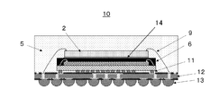
図1は本発明の実施形態1の半導体モジュール10を示す図である。
本発明に係る半導体モジュール10は、パッケージ基板(以下、第2パッケージ基板ともいう)12と、このパッケージ基板12に搭載された第1の半導体パッケージ6と、この第1の半導体パッケージ6に積層された半導体ベアチップ2とを樹脂5によって樹脂封止したものである。
第1の半導体パッケージ6の詳細を図2に基づいて説明する。
第1の半導体パッケージ6は第1パッケージ基板4上に半導体ベアチップ1を搭載し、ワイヤボンディングによってワイヤ9cで半導体ベアチップ1と第1パッケージ基板4とを電気的に接続した後、樹脂5aで樹脂封止したものである。
半導体ベアチップ1はウエハレベルでテストして良品とされたものを用いる。また、第1の半導体パッケージ6はパッケージの状態でテストされ良品とされたものを用いる。尚、必ずしもテストしている事を限定するものではない。
図3は第1パッケージ基板4の外観を示す図である。第1パッケージ基板4は実装用電極7と試験用電極8とを備えている。
本実施形態では、図1に示すように、まず、第2パッケージ基板12上に第1の半導体パッケージ6を搭載する。この搭載は、第1の半導体パッケージ6の第1パッケージ基板4の電極パッド7、8をパッケージ基板12の電極にはんだで接合することによって行われる。次いで、この第1の半導体パッケージ6の樹脂面上に半導体ベアチップ2を接着剤14によって接合することによって搭載し、ワイヤ9によって半導体ベアチップ2と第2パッケージ基板12とを電気的に接続した後、第1の半導体パッケージ6及び半導体ベアチップ2を樹脂5によって封止することによって第2の半導体パッケージ(半導体モジュール)を得る。
図12(b)に示される従来例では、半導体ベアチップ2と第1の半導体パッケージ6との隙間にワイヤが配置されているため、第1の半導体パッケージ6の反りによってワイヤが変形してワイヤショートを起こしたり、前記隙間が狭まって樹脂が隙間に充分に回り込まないという問題があったが、本実施形態では、第1の半導体パッケージ6がパッケージ基板12に電極7、8を介してはんだで接合されているため、第1の半導体パッケージ6の反りを矯正し、また、反りの発生を防止することができる。
また、半導体ベアチップ2が最上段にあるため、ワイヤボンディング作業は容易であり、ワイヤショートや樹脂未充填部分が形成されるという問題もない。
また、従来例では、第1パッケージ基板4の試験用電極8は、試験用のためのみに使用されていたが、本実施形態におけるように、第1パッケージ基板と第2パッケージ基板とを電極間ではんだ接合する場合には、第2パッケージ基板の配線を適宜に設計することにより試験用電極8を実装用電極として利用することができるという利点もある。
また、半導体ベアチップ2が最上段にあるため、ワイヤボンディング作業は容易であり、ワイヤショートや樹脂未充填部分が形成されるという問題もない。
また、従来例では、第1パッケージ基板4の試験用電極8は、試験用のためのみに使用されていたが、本実施形態におけるように、第1パッケージ基板と第2パッケージ基板とを電極間ではんだ接合する場合には、第2パッケージ基板の配線を適宜に設計することにより試験用電極8を実装用電極として利用することができるという利点もある。
(実施形態2)
図4は本発明の実施形態2の半導体モジュール20を示す図である。
本実施形態においては実施形態1と同様に、第1パッケージ基板4の電極パッド7、8をパッケージ基板12の電極にはんだで接合することによってパッケージ基板12に第1の半導体パッケージ6を搭載する。第1の半導体パッケージ6の樹脂面上に第1の半導体ベアチップ2が搭載され、更にこの第1の半導体ベアチップ2の上に第2の半導体ベアチップ3が搭載される。第1の半導体ベアチップ2と第2の半導体ベアチップ3とははんだなどの金属接合によって直接接続される、いわゆる微細ピッチ接続によるCOC(Chip On Chip)接続構造となっている。
図4は本発明の実施形態2の半導体モジュール20を示す図である。
本実施形態においては実施形態1と同様に、第1パッケージ基板4の電極パッド7、8をパッケージ基板12の電極にはんだで接合することによってパッケージ基板12に第1の半導体パッケージ6を搭載する。第1の半導体パッケージ6の樹脂面上に第1の半導体ベアチップ2が搭載され、更にこの第1の半導体ベアチップ2の上に第2の半導体ベアチップ3が搭載される。第1の半導体ベアチップ2と第2の半導体ベアチップ3とははんだなどの金属接合によって直接接続される、いわゆる微細ピッチ接続によるCOC(Chip On Chip)接続構造となっている。
(実施形態3)
図5は本発明の実施形態3の半導体モジュール30を示す図である。
本実施形態においては、実施形態1と同様に、第1の半導体パッケージ6の第1パッケージ基板4の電極パッド7、8を第2パッケージ基板12の電極にはんだで接合することによって第2パッケージ基板12に第1の半導体パッケージ6が搭載される。また、第1の半導体パッケージ6の樹脂面上に接着剤によって第1の半導体ベアチップ2が搭載され、更にこの上に接着剤によって第2の半導体ベアチップ3が搭載される。第1の半導体ベアチップ2と第2の半導体ベアチップ3とは、ワイヤ9aによって電気的に接続されており、第1の半導体ベアチップ2と第2パッケージ基板12とはワイヤ9によって電気的に接続されている。尚、第2の半導体ベアチップ3が第2パッケージ基板12と直接ワイヤ9aによって電気的に接続されることもある。
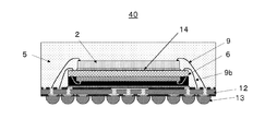
図6は本発明の実施形態4の半導体モジュール40を示す図である。
本実施形態では、第1の半導体パッケージ6の樹脂面側が第2パッケージ基板側となるようにして、第1の半導体パッケージ6と第2パッケージ基板12とが接着剤によって接合されている。このように、第1の半導体パッケージ6の樹脂面側が第2パッケージ基板側となるにようにして第1の半導体パッケージ6と第2パッケージ基板12とを接合することによっても第1の半導体パッケージ6の反りを矯正し、また、反りの発生を防止することができる。
この第1の半導体パッケージ6の樹脂面とは反対側の面の上に半導体ベアチップ2が接着剤14によって接合され搭載されている。この第1の半導体パッケージはワイヤ9bによって第2パッケージ基板12に電気的に接続され、半導体ベアチップ2は9によって第2パッケージ基板12に電気的に接続されている。
図7は本発明の実施形態5の半導体モジュール50を示す図である。
本実施形態では、第1の半導体パッケージ6の樹脂面側が第2パッケージ基板側となるにようにして、第1の半導体パッケージ6と第2パッケージ基板12とが接着剤によって接合されている。第1の半導体パッケージ6の樹脂面とは反対側の面上に第1の半導体ベアチップ2が搭載されている。更に、この第1の半導体ベアチップ2上には、第2の半導体ベアチップ3が搭載されている。第1の半導体ベアチップ2と第2の半導体ベアチップ3とは、はんだ11などの金属接合により電気的に直接接続されている。
また、第1の半導体パッケージ6はワイヤ9bによって第2パッケージ基板12に電気的に接続され、第1の半導体ベアチップ2はワイヤ9によって第2パッケージ基板12に電気的に接続されている。
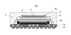
図8は本発明の実施形態6の半導体モジュール60を示す図である。
本実施形態では、第1の半導体パッケージ6の樹脂面側が第2パッケージ基板側となるにようにして、第1の半導体パッケージ6と第2パッケージ基板12とが接着剤によって接合されている。第1の半導体パッケージの樹脂面とは反対側の面上に第1の半導体ベアチップ2が接着剤によって接合されて搭載されており、この第1の半導体ベアチップ2上には第2の半導体ベアチップ3が接着剤によって接合されて搭載されている。第1の半導体ベアチップ2と第2の半導体ベアチップ3とは、ワイヤ9aによって電気的に接続されており、第1の半導体ベアチップ2と第2パッケージ基板12とはワイヤ9によって電気的に接続されており、第1の半導体パッケージ6と第2パッケージ基板12とはワイヤ9bによって電気的に接続されている。尚、第2の半導体ベアチップ3が第2パッケージ基板12と直接ワイヤ9aによって電気的に接続されることもある。
本実施形態では、第1の半導体パッケージ6の樹脂面側が第2パッケージ基板側となるにようにして、第1の半導体パッケージ6と第2パッケージ基板12とが接着剤によって接合されている。第1の半導体パッケージの樹脂面とは反対側の面上に第1の半導体ベアチップ2が接着剤によって接合されて搭載されており、この第1の半導体ベアチップ2上には第2の半導体ベアチップ3が接着剤によって接合されて搭載されている。第1の半導体ベアチップ2と第2の半導体ベアチップ3とは、ワイヤ9aによって電気的に接続されており、第1の半導体ベアチップ2と第2パッケージ基板12とはワイヤ9によって電気的に接続されており、第1の半導体パッケージ6と第2パッケージ基板12とはワイヤ9bによって電気的に接続されている。尚、第2の半導体ベアチップ3が第2パッケージ基板12と直接ワイヤ9aによって電気的に接続されることもある。
図9は本発明の実施形態7の半導体モジュール70を示す図である。
本実施形態では、第1の半導体パッケージ6の上にスペーサー15を搭載し、その上に半導体ベアチップ2を搭載している。なお、図9では第1の半導体パッケージ6と第2パッケージ基板12との電気的接続構造及び半導体ベアチップ2と第2パッケージ基板12との電気的接続構造は図示していない。第1の半導体パッケージ6と第2パッケージ基板12とは、第1の半導体パッケージ6の電極側で接合しても良いし、第1の半導体パッケージ6の樹脂面側で接合しても良い。
スペーサー15を設けることにより、半導体ベアチップ2と第1の半導体パッケージ6との大きさに差異がない場合でも第1の半導体パッケージ6とパッケージ基板12とのワイヤボンディングが可能となる。
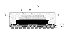
図10は本発明の実施形態8の半導体モジュール80を示す図である。
本実施形態では、第1の半導体パッケージ6の上に半導体ベアチップ2が搭載されており、この半導体ベアチップ2の上にシリコン板又はCu板等の放熱板16を搭載している。
図示例では放熱板16を半導体ベアチップの上に搭載しているが、放熱板16を設ける位置は半導体ベアチップ2の上に限定されるものではない。
なお、図10では第1の半導体パッケージ6とパッケージ基板12との電気的接続構造及び半導体ベアチップ2とパッケージ基板12との電気的接続構造は図示していない。
第1の半導体パッケージ6と第2パッケージ基板12とは、第1の半導体パッケージ6の電極側で接合しても良いし、第1の半導体パッケージ6の樹脂面側で接合しても良い。
このような放熱板16を設けることにより半導体モジュールの放熱特性を高めることができる。
図11は本発明の実施形態9の半導体モジュール90を示す図である。
本実施態様では第2パッケージ基板12の中に半導体ベアチップ2が実装され、この第2パッケージ基板12に第1の半導体パッケージ6を接合したのち樹脂5で封止して半導体モジュール90としている。
この実施態様によれば、半導体ベアチップ2の厚さを第2パッケージ基板12の中で吸収出来るため、半導体モジュール90を薄厚化する事が可能となる。
本実施態様では第2パッケージ基板12の中に半導体ベアチップ2が実装され、この第2パッケージ基板12に第1の半導体パッケージ6を接合したのち樹脂5で封止して半導体モジュール90としている。
この実施態様によれば、半導体ベアチップ2の厚さを第2パッケージ基板12の中で吸収出来るため、半導体モジュール90を薄厚化する事が可能となる。
1,1a,1b 半導体ベアチップ
2 第1の半導体ベアチップ
3 第2の半導体ベアチップ
4 第1パッケージ基板
5,5a 樹脂
6 第1の半導体パッケージ
7 電極パッド(実装用電極)
8 電極パッド(試験用電極)
9,9a,9b,9c ワイヤ
11 はんだ
12 第2パッケージ基板
13 はんだボール
14 接着剤
15 スペーサー
16 放熱板
10,20,30,40,50,60,70,80 半導体モジュール
2 第1の半導体ベアチップ
3 第2の半導体ベアチップ
4 第1パッケージ基板
5,5a 樹脂
6 第1の半導体パッケージ
7 電極パッド(実装用電極)
8 電極パッド(試験用電極)
9,9a,9b,9c ワイヤ
11 はんだ
12 第2パッケージ基板
13 はんだボール
14 接着剤
15 スペーサー
16 放熱板
10,20,30,40,50,60,70,80 半導体モジュール
Claims (9)
- 第1パッケージ基板に半導体ベアチップを搭載して樹脂封止してなる半導体パッケージと、半導体ベアチップと、第2パッケージ基板とを有する半導体モジュールであって、前記第2パッケージ基板に前記半導体パッケージが搭載されており、前記半導体パッケージ上に前記半導体ベアチップが搭載されていることを特徴とする半導体モジュール。
- 前記半導体パッケージは、樹脂面とは反対の側の面で電極パッドを介してはんだにより第2パッケージ基板と電気的に接続されていることを特徴とする請求項1に記載の半導体モジュール。
- 前記半導体パッケージは、樹脂面で第2パッケージ基板と接合されており、ワイヤボンディングにより第2パッケージ基板と電気的に接続されていることを特徴とする請求項1に記載の半導体モジュール。
- 前記半導体パッケージ上に搭載された半導体ベアチップは第2パッケージ基板とワイヤボンディングにより電気的に接続されていることを特徴とする請求項1〜3のいずれかに記載の半導体モジュール。
- 前記半導体パッケージ上には前記半導体ベアチップが2個以上積層して搭載されており、前記半導体ベアチップ間の電気的接続はCOC構造をとっていることを特徴とする請求項1〜4のいずれかに記載の半導体モジュール。
- 前記半導体パッケージ上には前記半導体ベアチップが2個以上積層して搭載されており、前記半導体ベアチップ間はワイヤボンディングにより電気的に接続されていることを特徴とする請求項1〜4のいずれかに記載の半導体モジュール。
- 前記半導体ベアチップがスペーサーを介して前記半導体パッケージ上に搭載されていることを特徴とする請求項1〜6のいずれかに記載の半導体モジュール。
- 前記半導体ベアチップの上に放熱板が搭載されていることを特徴とする請求項1〜7のいずれかに記載の半導体モジュール。
- 前記半導体パッケージは、第1パッケージ基板上に複数個の半導体ベアチップを搭載していることを特徴とする請求項1〜8のいずれかに記載の半導体モジュール。
Priority Applications (7)
| Application Number | Priority Date | Filing Date | Title |
|---|---|---|---|
| JP2012080570A JP2013211407A (ja) | 2012-03-30 | 2012-03-30 | 半導体モジュール |
| US13/778,936 US20130256865A1 (en) | 2012-03-30 | 2013-02-27 | Semiconductor module |
| EP13157205.9A EP2645417A1 (en) | 2012-03-30 | 2013-02-28 | Semiconductor module |
| EP14162557.4A EP2752873A3 (en) | 2012-03-30 | 2013-02-28 | Semiconductor module |
| TW102110840A TW201349443A (zh) | 2012-03-30 | 2013-03-27 | 半導體模組 |
| KR1020130033407A KR20130111401A (ko) | 2012-03-30 | 2013-03-28 | 반도체 모듈 |
| CN201310106918XA CN103367272A (zh) | 2012-03-30 | 2013-03-29 | 半导体模块 |
Applications Claiming Priority (1)
| Application Number | Priority Date | Filing Date | Title |
|---|---|---|---|
| JP2012080570A JP2013211407A (ja) | 2012-03-30 | 2012-03-30 | 半導体モジュール |
Publications (1)
| Publication Number | Publication Date |
|---|---|
| JP2013211407A true JP2013211407A (ja) | 2013-10-10 |
Family
ID=47884150
Family Applications (1)
| Application Number | Title | Priority Date | Filing Date |
|---|---|---|---|
| JP2012080570A Pending JP2013211407A (ja) | 2012-03-30 | 2012-03-30 | 半導体モジュール |
Country Status (6)
| Country | Link |
|---|---|
| US (1) | US20130256865A1 (ja) |
| EP (2) | EP2645417A1 (ja) |
| JP (1) | JP2013211407A (ja) |
| KR (1) | KR20130111401A (ja) |
| CN (1) | CN103367272A (ja) |
| TW (1) | TW201349443A (ja) |
Families Citing this family (11)
| Publication number | Priority date | Publication date | Assignee | Title |
|---|---|---|---|---|
| US10847488B2 (en) | 2015-11-02 | 2020-11-24 | Mediatek Inc. | Semiconductor package having multi-tier bonding wires and components directly mounted on the multi-tier bonding wires |
| JP6678506B2 (ja) * | 2016-04-28 | 2020-04-08 | 株式会社アムコー・テクノロジー・ジャパン | 半導体パッケージ及び半導体パッケージの製造方法 |
| US10804115B2 (en) * | 2017-08-03 | 2020-10-13 | General Electric Company | Electronics package with integrated interconnect structure and method of manufacturing thereof |
| US10541209B2 (en) * | 2017-08-03 | 2020-01-21 | General Electric Company | Electronics package including integrated electromagnetic interference shield and method of manufacturing thereof |
| US10541153B2 (en) * | 2017-08-03 | 2020-01-21 | General Electric Company | Electronics package with integrated interconnect structure and method of manufacturing thereof |
| JP7198921B2 (ja) | 2018-10-11 | 2023-01-11 | 長江存儲科技有限責任公司 | 半導体デバイスおよび方法 |
| EP3834227A4 (en) * | 2018-10-30 | 2022-03-30 | Yangtze Memory Technologies Co., Ltd. | IC PACKAGE |
| KR102554692B1 (ko) | 2019-02-18 | 2023-07-12 | 양쯔 메모리 테크놀로지스 씨오., 엘티디. | 집적 구조체 및 형성 방법 |
| JP2021015922A (ja) * | 2019-07-16 | 2021-02-12 | キオクシア株式会社 | 半導体装置およびその製造方法 |
| US11355450B2 (en) * | 2019-08-01 | 2022-06-07 | Mediatek Inc. | Semiconductor package with EMI shielding structure |
| US11456231B2 (en) * | 2021-01-18 | 2022-09-27 | Fortinet, Inc. | Heatsink arrangement for integrated circuit assembly and method for assembling thereof |
Citations (6)
| Publication number | Priority date | Publication date | Assignee | Title |
|---|---|---|---|---|
| US6946323B1 (en) * | 2001-11-02 | 2005-09-20 | Amkor Technology, Inc. | Semiconductor package having one or more die stacked on a prepackaged device and method therefor |
| JP2006049569A (ja) * | 2004-08-04 | 2006-02-16 | Sharp Corp | スタック型半導体装置パッケージおよびその製造方法 |
| US20060097402A1 (en) * | 2004-11-08 | 2006-05-11 | Siliconware Precision Industries Co., Ltd. | Semiconductor device having flip-chip package and method for fabricating the same |
| JP2006216911A (ja) * | 2005-02-07 | 2006-08-17 | Renesas Technology Corp | 半導体装置およびカプセル型半導体パッケージ |
| JP2008192714A (ja) * | 2007-02-02 | 2008-08-21 | Toshiba Corp | 半導体パッケージ |
| JP2012015225A (ja) * | 2010-06-30 | 2012-01-19 | Hitachi Ltd | 半導体装置 |
Family Cites Families (5)
| Publication number | Priority date | Publication date | Assignee | Title |
|---|---|---|---|---|
| JP2002040095A (ja) | 2000-07-26 | 2002-02-06 | Nec Corp | 半導体装置及びその実装方法 |
| US7049691B2 (en) | 2002-10-08 | 2006-05-23 | Chippac, Inc. | Semiconductor multi-package module having inverted second package and including additional die or stacked package on second package |
| US7582960B2 (en) * | 2005-05-05 | 2009-09-01 | Stats Chippac Ltd. | Multiple chip package module including die stacked over encapsulated package |
| US7843058B2 (en) * | 2007-10-30 | 2010-11-30 | Taiwan Semiconductor Manufacturing Company, Ltd. | Flip chip packages with spacers separating heat sinks and substrates |
| JP4303772B2 (ja) | 2008-06-17 | 2009-07-29 | 株式会社Genusion | 半導体パッケージ |
-
2012
- 2012-03-30 JP JP2012080570A patent/JP2013211407A/ja active Pending
-
2013
- 2013-02-27 US US13/778,936 patent/US20130256865A1/en not_active Abandoned
- 2013-02-28 EP EP13157205.9A patent/EP2645417A1/en not_active Withdrawn
- 2013-02-28 EP EP14162557.4A patent/EP2752873A3/en not_active Withdrawn
- 2013-03-27 TW TW102110840A patent/TW201349443A/zh unknown
- 2013-03-28 KR KR1020130033407A patent/KR20130111401A/ko not_active Application Discontinuation
- 2013-03-29 CN CN201310106918XA patent/CN103367272A/zh active Pending
Patent Citations (6)
| Publication number | Priority date | Publication date | Assignee | Title |
|---|---|---|---|---|
| US6946323B1 (en) * | 2001-11-02 | 2005-09-20 | Amkor Technology, Inc. | Semiconductor package having one or more die stacked on a prepackaged device and method therefor |
| JP2006049569A (ja) * | 2004-08-04 | 2006-02-16 | Sharp Corp | スタック型半導体装置パッケージおよびその製造方法 |
| US20060097402A1 (en) * | 2004-11-08 | 2006-05-11 | Siliconware Precision Industries Co., Ltd. | Semiconductor device having flip-chip package and method for fabricating the same |
| JP2006216911A (ja) * | 2005-02-07 | 2006-08-17 | Renesas Technology Corp | 半導体装置およびカプセル型半導体パッケージ |
| JP2008192714A (ja) * | 2007-02-02 | 2008-08-21 | Toshiba Corp | 半導体パッケージ |
| JP2012015225A (ja) * | 2010-06-30 | 2012-01-19 | Hitachi Ltd | 半導体装置 |
Also Published As
| Publication number | Publication date |
|---|---|
| EP2645417A1 (en) | 2013-10-02 |
| TW201349443A (zh) | 2013-12-01 |
| EP2752873A3 (en) | 2014-09-24 |
| CN103367272A (zh) | 2013-10-23 |
| US20130256865A1 (en) | 2013-10-03 |
| KR20130111401A (ko) | 2013-10-10 |
| EP2752873A2 (en) | 2014-07-09 |
Similar Documents
| Publication | Publication Date | Title |
|---|---|---|
| JP2013211407A (ja) | 半導体モジュール | |
| US9548220B2 (en) | Method of fabricating semiconductor package having an interposer structure | |
| US20150041969A1 (en) | Semiconductor package and fabrication method thereof | |
| US9082644B2 (en) | Method of manufacturing and testing a chip package | |
| TW201436161A (zh) | 半導體封裝件及其製法 | |
| US20170005030A1 (en) | Flat No-Leads Package With Improved Contact Pins | |
| US20120168936A1 (en) | Multi-chip stack package structure and fabrication method thereof | |
| US20110175212A1 (en) | Dual die semiconductor package | |
| JP6128993B2 (ja) | 積層型半導体装置、プリント回路板、電子機器及び積層型半導体装置の製造方法 | |
| US6818999B2 (en) | Semiconductor device having multiple semiconductor chips in a single package | |
| JP5547703B2 (ja) | 半導体装置の製造方法 | |
| JP4388926B2 (ja) | 半導体装置のパッケージ構造 | |
| TW201523832A (zh) | 半導體封裝件之製法 | |
| JP2010010269A (ja) | 半導体装置、半導体装置製造用中間体およびそれらの製造方法 | |
| TWI555101B (zh) | 封裝結構及其製法 | |
| JP2008277457A (ja) | 積層型半導体装置および実装体 | |
| JP3842272B2 (ja) | インターポーザー、半導体チップマウントサブ基板および半導体パッケージ | |
| JP2007142128A (ja) | 半導体装置およびその製造方法 | |
| US20120223425A1 (en) | Semiconductor device and fabrication method thereof | |
| JP4303772B2 (ja) | 半導体パッケージ | |
| JP4439339B2 (ja) | 半導体装置およびその製造方法 | |
| JP2011119619A (ja) | 半導体パッケージ | |
| JP4388989B2 (ja) | 半導体チップマウント封止サブ基板 | |
| KR100762875B1 (ko) | 적층형 패키지 | |
| KR20150090442A (ko) | 반도체 장치 및 이의 제조 방법 |
Legal Events
| Date | Code | Title | Description |
|---|---|---|---|
| A621 | Written request for application examination |
Free format text: JAPANESE INTERMEDIATE CODE: A621 Effective date: 20150203 |
|
| A977 | Report on retrieval |
Free format text: JAPANESE INTERMEDIATE CODE: A971007 Effective date: 20151026 |
|
| A131 | Notification of reasons for refusal |
Free format text: JAPANESE INTERMEDIATE CODE: A131 Effective date: 20151106 |
|
| A02 | Decision of refusal |
Free format text: JAPANESE INTERMEDIATE CODE: A02 Effective date: 20160301 |