JP2013197531A - 半導体装置およびその製造方法 - Google Patents
半導体装置およびその製造方法 Download PDFInfo
- Publication number
- JP2013197531A JP2013197531A JP2012066194A JP2012066194A JP2013197531A JP 2013197531 A JP2013197531 A JP 2013197531A JP 2012066194 A JP2012066194 A JP 2012066194A JP 2012066194 A JP2012066194 A JP 2012066194A JP 2013197531 A JP2013197531 A JP 2013197531A
- Authority
- JP
- Japan
- Prior art keywords
- resin
- semiconductor chip
- semiconductor device
- protective resin
- bonding wire
- Prior art date
- Legal status (The legal status is an assumption and is not a legal conclusion. Google has not performed a legal analysis and makes no representation as to the accuracy of the status listed.)
- Pending
Links
Images


Classifications
-
- H—ELECTRICITY
- H01—ELECTRIC ELEMENTS
- H01L—SEMICONDUCTOR DEVICES NOT COVERED BY CLASS H10
- H01L24/00—Arrangements for connecting or disconnecting semiconductor or solid-state bodies; Methods or apparatus related thereto
- H01L24/80—Methods for connecting semiconductor or other solid state bodies using means for bonding being attached to, or being formed on, the surface to be connected
- H01L24/85—Methods for connecting semiconductor or other solid state bodies using means for bonding being attached to, or being formed on, the surface to be connected using a wire connector
-
- H—ELECTRICITY
- H01—ELECTRIC ELEMENTS
- H01L—SEMICONDUCTOR DEVICES NOT COVERED BY CLASS H10
- H01L2224/00—Indexing scheme for arrangements for connecting or disconnecting semiconductor or solid-state bodies and methods related thereto as covered by H01L24/00
- H01L2224/01—Means for bonding being attached to, or being formed on, the surface to be connected, e.g. chip-to-package, die-attach, "first-level" interconnects; Manufacturing methods related thereto
- H01L2224/02—Bonding areas; Manufacturing methods related thereto
- H01L2224/04—Structure, shape, material or disposition of the bonding areas prior to the connecting process
- H01L2224/05—Structure, shape, material or disposition of the bonding areas prior to the connecting process of an individual bonding area
- H01L2224/0554—External layer
- H01L2224/05599—Material
- H01L2224/056—Material with a principal constituent of the material being a metal or a metalloid, e.g. boron [B], silicon [Si], germanium [Ge], arsenic [As], antimony [Sb], tellurium [Te] and polonium [Po], and alloys thereof
- H01L2224/05617—Material with a principal constituent of the material being a metal or a metalloid, e.g. boron [B], silicon [Si], germanium [Ge], arsenic [As], antimony [Sb], tellurium [Te] and polonium [Po], and alloys thereof the principal constituent melting at a temperature of greater than or equal to 400°C and less than 950°C
- H01L2224/05624—Aluminium [Al] as principal constituent
-
- H—ELECTRICITY
- H01—ELECTRIC ELEMENTS
- H01L—SEMICONDUCTOR DEVICES NOT COVERED BY CLASS H10
- H01L2224/00—Indexing scheme for arrangements for connecting or disconnecting semiconductor or solid-state bodies and methods related thereto as covered by H01L24/00
- H01L2224/01—Means for bonding being attached to, or being formed on, the surface to be connected, e.g. chip-to-package, die-attach, "first-level" interconnects; Manufacturing methods related thereto
- H01L2224/26—Layer connectors, e.g. plate connectors, solder or adhesive layers; Manufacturing methods related thereto
- H01L2224/31—Structure, shape, material or disposition of the layer connectors after the connecting process
- H01L2224/32—Structure, shape, material or disposition of the layer connectors after the connecting process of an individual layer connector
- H01L2224/321—Disposition
- H01L2224/32151—Disposition the layer connector connecting between a semiconductor or solid-state body and an item not being a semiconductor or solid-state body, e.g. chip-to-substrate, chip-to-passive
- H01L2224/32221—Disposition the layer connector connecting between a semiconductor or solid-state body and an item not being a semiconductor or solid-state body, e.g. chip-to-substrate, chip-to-passive the body and the item being stacked
- H01L2224/32225—Disposition the layer connector connecting between a semiconductor or solid-state body and an item not being a semiconductor or solid-state body, e.g. chip-to-substrate, chip-to-passive the body and the item being stacked the item being non-metallic, e.g. insulating substrate with or without metallisation
-
- H—ELECTRICITY
- H01—ELECTRIC ELEMENTS
- H01L—SEMICONDUCTOR DEVICES NOT COVERED BY CLASS H10
- H01L2224/00—Indexing scheme for arrangements for connecting or disconnecting semiconductor or solid-state bodies and methods related thereto as covered by H01L24/00
- H01L2224/01—Means for bonding being attached to, or being formed on, the surface to be connected, e.g. chip-to-package, die-attach, "first-level" interconnects; Manufacturing methods related thereto
- H01L2224/42—Wire connectors; Manufacturing methods related thereto
- H01L2224/44—Structure, shape, material or disposition of the wire connectors prior to the connecting process
- H01L2224/45—Structure, shape, material or disposition of the wire connectors prior to the connecting process of an individual wire connector
- H01L2224/45001—Core members of the connector
- H01L2224/45099—Material
- H01L2224/451—Material with a principal constituent of the material being a metal or a metalloid, e.g. boron (B), silicon (Si), germanium (Ge), arsenic (As), antimony (Sb), tellurium (Te) and polonium (Po), and alloys thereof
- H01L2224/45117—Material with a principal constituent of the material being a metal or a metalloid, e.g. boron (B), silicon (Si), germanium (Ge), arsenic (As), antimony (Sb), tellurium (Te) and polonium (Po), and alloys thereof the principal constituent melting at a temperature of greater than or equal to 400°C and less than 950°C
- H01L2224/45124—Aluminium (Al) as principal constituent
-
- H—ELECTRICITY
- H01—ELECTRIC ELEMENTS
- H01L—SEMICONDUCTOR DEVICES NOT COVERED BY CLASS H10
- H01L2224/00—Indexing scheme for arrangements for connecting or disconnecting semiconductor or solid-state bodies and methods related thereto as covered by H01L24/00
- H01L2224/01—Means for bonding being attached to, or being formed on, the surface to be connected, e.g. chip-to-package, die-attach, "first-level" interconnects; Manufacturing methods related thereto
- H01L2224/42—Wire connectors; Manufacturing methods related thereto
- H01L2224/44—Structure, shape, material or disposition of the wire connectors prior to the connecting process
- H01L2224/45—Structure, shape, material or disposition of the wire connectors prior to the connecting process of an individual wire connector
- H01L2224/45001—Core members of the connector
- H01L2224/45099—Material
- H01L2224/451—Material with a principal constituent of the material being a metal or a metalloid, e.g. boron (B), silicon (Si), germanium (Ge), arsenic (As), antimony (Sb), tellurium (Te) and polonium (Po), and alloys thereof
- H01L2224/45138—Material with a principal constituent of the material being a metal or a metalloid, e.g. boron (B), silicon (Si), germanium (Ge), arsenic (As), antimony (Sb), tellurium (Te) and polonium (Po), and alloys thereof the principal constituent melting at a temperature of greater than or equal to 950°C and less than 1550°C
- H01L2224/45147—Copper (Cu) as principal constituent
-
- H—ELECTRICITY
- H01—ELECTRIC ELEMENTS
- H01L—SEMICONDUCTOR DEVICES NOT COVERED BY CLASS H10
- H01L2224/00—Indexing scheme for arrangements for connecting or disconnecting semiconductor or solid-state bodies and methods related thereto as covered by H01L24/00
- H01L2224/01—Means for bonding being attached to, or being formed on, the surface to be connected, e.g. chip-to-package, die-attach, "first-level" interconnects; Manufacturing methods related thereto
- H01L2224/42—Wire connectors; Manufacturing methods related thereto
- H01L2224/47—Structure, shape, material or disposition of the wire connectors after the connecting process
- H01L2224/48—Structure, shape, material or disposition of the wire connectors after the connecting process of an individual wire connector
- H01L2224/4805—Shape
- H01L2224/4809—Loop shape
- H01L2224/48091—Arched
-
- H—ELECTRICITY
- H01—ELECTRIC ELEMENTS
- H01L—SEMICONDUCTOR DEVICES NOT COVERED BY CLASS H10
- H01L2224/00—Indexing scheme for arrangements for connecting or disconnecting semiconductor or solid-state bodies and methods related thereto as covered by H01L24/00
- H01L2224/01—Means for bonding being attached to, or being formed on, the surface to be connected, e.g. chip-to-package, die-attach, "first-level" interconnects; Manufacturing methods related thereto
- H01L2224/42—Wire connectors; Manufacturing methods related thereto
- H01L2224/47—Structure, shape, material or disposition of the wire connectors after the connecting process
- H01L2224/48—Structure, shape, material or disposition of the wire connectors after the connecting process of an individual wire connector
- H01L2224/481—Disposition
- H01L2224/48151—Connecting between a semiconductor or solid-state body and an item not being a semiconductor or solid-state body, e.g. chip-to-substrate, chip-to-passive
- H01L2224/48221—Connecting between a semiconductor or solid-state body and an item not being a semiconductor or solid-state body, e.g. chip-to-substrate, chip-to-passive the body and the item being stacked
- H01L2224/48225—Connecting between a semiconductor or solid-state body and an item not being a semiconductor or solid-state body, e.g. chip-to-substrate, chip-to-passive the body and the item being stacked the item being non-metallic, e.g. insulating substrate with or without metallisation
- H01L2224/48227—Connecting between a semiconductor or solid-state body and an item not being a semiconductor or solid-state body, e.g. chip-to-substrate, chip-to-passive the body and the item being stacked the item being non-metallic, e.g. insulating substrate with or without metallisation connecting the wire to a bond pad of the item
-
- H—ELECTRICITY
- H01—ELECTRIC ELEMENTS
- H01L—SEMICONDUCTOR DEVICES NOT COVERED BY CLASS H10
- H01L2224/00—Indexing scheme for arrangements for connecting or disconnecting semiconductor or solid-state bodies and methods related thereto as covered by H01L24/00
- H01L2224/01—Means for bonding being attached to, or being formed on, the surface to be connected, e.g. chip-to-package, die-attach, "first-level" interconnects; Manufacturing methods related thereto
- H01L2224/42—Wire connectors; Manufacturing methods related thereto
- H01L2224/47—Structure, shape, material or disposition of the wire connectors after the connecting process
- H01L2224/48—Structure, shape, material or disposition of the wire connectors after the connecting process of an individual wire connector
- H01L2224/481—Disposition
- H01L2224/48151—Connecting between a semiconductor or solid-state body and an item not being a semiconductor or solid-state body, e.g. chip-to-substrate, chip-to-passive
- H01L2224/48221—Connecting between a semiconductor or solid-state body and an item not being a semiconductor or solid-state body, e.g. chip-to-substrate, chip-to-passive the body and the item being stacked
- H01L2224/48245—Connecting between a semiconductor or solid-state body and an item not being a semiconductor or solid-state body, e.g. chip-to-substrate, chip-to-passive the body and the item being stacked the item being metallic
- H01L2224/48247—Connecting between a semiconductor or solid-state body and an item not being a semiconductor or solid-state body, e.g. chip-to-substrate, chip-to-passive the body and the item being stacked the item being metallic connecting the wire to a bond pad of the item
-
- H—ELECTRICITY
- H01—ELECTRIC ELEMENTS
- H01L—SEMICONDUCTOR DEVICES NOT COVERED BY CLASS H10
- H01L2224/00—Indexing scheme for arrangements for connecting or disconnecting semiconductor or solid-state bodies and methods related thereto as covered by H01L24/00
- H01L2224/01—Means for bonding being attached to, or being formed on, the surface to be connected, e.g. chip-to-package, die-attach, "first-level" interconnects; Manufacturing methods related thereto
- H01L2224/42—Wire connectors; Manufacturing methods related thereto
- H01L2224/47—Structure, shape, material or disposition of the wire connectors after the connecting process
- H01L2224/48—Structure, shape, material or disposition of the wire connectors after the connecting process of an individual wire connector
- H01L2224/485—Material
- H01L2224/48505—Material at the bonding interface
- H01L2224/48699—Principal constituent of the connecting portion of the wire connector being Aluminium (Al)
- H01L2224/487—Principal constituent of the connecting portion of the wire connector being Aluminium (Al) with a principal constituent of the bonding area being a metal or a metalloid, e.g. boron (B), silicon (Si), germanium (Ge), arsenic (As), antimony (Sb), tellurium (Te) and polonium (Po), and alloys thereof
- H01L2224/48717—Principal constituent of the connecting portion of the wire connector being Aluminium (Al) with a principal constituent of the bonding area being a metal or a metalloid, e.g. boron (B), silicon (Si), germanium (Ge), arsenic (As), antimony (Sb), tellurium (Te) and polonium (Po), and alloys thereof the principal constituent melting at a temperature of greater than or equal to 400°C and less than 950 °C
- H01L2224/48724—Aluminium (Al) as principal constituent
-
- H—ELECTRICITY
- H01—ELECTRIC ELEMENTS
- H01L—SEMICONDUCTOR DEVICES NOT COVERED BY CLASS H10
- H01L2224/00—Indexing scheme for arrangements for connecting or disconnecting semiconductor or solid-state bodies and methods related thereto as covered by H01L24/00
- H01L2224/73—Means for bonding being of different types provided for in two or more of groups H01L2224/10, H01L2224/18, H01L2224/26, H01L2224/34, H01L2224/42, H01L2224/50, H01L2224/63, H01L2224/71
- H01L2224/732—Location after the connecting process
- H01L2224/73251—Location after the connecting process on different surfaces
- H01L2224/73265—Layer and wire connectors
-
- H—ELECTRICITY
- H01—ELECTRIC ELEMENTS
- H01L—SEMICONDUCTOR DEVICES NOT COVERED BY CLASS H10
- H01L2224/00—Indexing scheme for arrangements for connecting or disconnecting semiconductor or solid-state bodies and methods related thereto as covered by H01L24/00
- H01L2224/80—Methods for connecting semiconductor or other solid state bodies using means for bonding being attached to, or being formed on, the surface to be connected
- H01L2224/85—Methods for connecting semiconductor or other solid state bodies using means for bonding being attached to, or being formed on, the surface to be connected using a wire connector
- H01L2224/852—Applying energy for connecting
- H01L2224/85201—Compression bonding
- H01L2224/85203—Thermocompression bonding
-
- H—ELECTRICITY
- H01—ELECTRIC ELEMENTS
- H01L—SEMICONDUCTOR DEVICES NOT COVERED BY CLASS H10
- H01L2224/00—Indexing scheme for arrangements for connecting or disconnecting semiconductor or solid-state bodies and methods related thereto as covered by H01L24/00
- H01L2224/80—Methods for connecting semiconductor or other solid state bodies using means for bonding being attached to, or being formed on, the surface to be connected
- H01L2224/85—Methods for connecting semiconductor or other solid state bodies using means for bonding being attached to, or being formed on, the surface to be connected using a wire connector
- H01L2224/85909—Post-treatment of the connector or wire bonding area
- H01L2224/8592—Applying permanent coating, e.g. protective coating
-
- H—ELECTRICITY
- H01—ELECTRIC ELEMENTS
- H01L—SEMICONDUCTOR DEVICES NOT COVERED BY CLASS H10
- H01L2924/00—Indexing scheme for arrangements or methods for connecting or disconnecting semiconductor or solid-state bodies as covered by H01L24/00
- H01L2924/15—Details of package parts other than the semiconductor or other solid state devices to be connected
- H01L2924/151—Die mounting substrate
- H01L2924/153—Connection portion
- H01L2924/1531—Connection portion the connection portion being formed only on the surface of the substrate opposite to the die mounting surface
- H01L2924/15311—Connection portion the connection portion being formed only on the surface of the substrate opposite to the die mounting surface being a ball array, e.g. BGA
-
- H—ELECTRICITY
- H01—ELECTRIC ELEMENTS
- H01L—SEMICONDUCTOR DEVICES NOT COVERED BY CLASS H10
- H01L2924/00—Indexing scheme for arrangements or methods for connecting or disconnecting semiconductor or solid-state bodies as covered by H01L24/00
- H01L2924/15—Details of package parts other than the semiconductor or other solid state devices to be connected
- H01L2924/181—Encapsulation
Abstract
【解決手段】半導体チップ、該チップを搭載する載置板、該チップと該載置板とを接続するワイヤ、及び、該チップと該載置板の該チップの搭載面と該ワイヤとを封止する樹脂封止体を備え、該ワイヤと半導体装置の各パーツとの接合部の何れかが、保護樹脂により被覆され、該保護樹脂の表面全体が該樹脂封止体により覆われる。
【選択図】図1
Description
(半導体装置10)
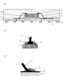
本発明に係る第1の実施形態について、図1を用いて説明する。
半導体チップ1は、半導体チップ1の裏面が接続パッド8の上面に接するように接続パッド8を介して回路基板2上に搭載されている。半導体チップ1の上面において、ボンディングワイヤ7がワイヤボンディング法を用いて半導体チップ1に電気的に接続されており、半導体チップ1とボンディングワイヤ7との接合部が、保護樹脂5により被覆されている。ここで、図1(b)は、図1(a)における半導体チップ1とボンディングワイヤ7との接合部における拡大図を示している。図1(b)に示すように、半導体チップ1は、半導体チップ1の上面において、具体的には電気接点9を介してボンディングワイヤ7の一端に電気的に接続されている。また、半導体チップ1とボンディングワイヤ7との接合部は、保護樹脂5により電気接点9を含むように被覆されている。
回路基板2は、回路基板2の裏面側に外部電極端子6を備えている。また、回路基板2は、回路基板2の上面および内部に配線11を備えている。更に、回路基板2は、回路基板2の上面に配線11を介して接続パッド8を備えている。図1(a)に示すように、接続パッド8の裏面の全体が配線11に接続されている必要はなく、接続パッド8の一部が配線11に接続されていればよいが、接続パッド8の裏面の全体が配線11に接続されていてもよい。また、回路基板2は、接続パッド8を介して半導体チップ1に接続されている。
ボンディングワイヤ7は、半導体チップ1と回路基板2とを電気的に接続するために用いられている。具体的には、ボンディングワイヤ7の一端が半導体チップ1の上面に電気接点9を介して電気的に接続されており、ボンディングワイヤ7の他端が回路基板2の上面に配線11を介して電気的に接続されている。この電気的な接続には、ワイヤボンディング法が用いられている。なお、本実施形態にて用いられるワイヤボンディングの種類は特に限定されず、ボールボンディング、ステッチボンディング等のあらゆる種類のワイヤボンディングが用いられ得る。
外部電極端子6は、球形状をしており、回路基板2の裏面側に設けられている。外部電極端子6の何れかが、配線11に接続されており、これにより、半導体チップ1を駆動させるための電力が、外部電極端子6から配線11およびボンディングワイヤ7を介して半導体チップ1に供給される。
接続パッド8は、配線11を介して回路基板2の上面に接続されている。
配線11は、回路基板2の上面および内部に設けられている。図1(c)に示すように、配線11を介して、回路基板2とボンディングワイヤとが接続されており、回路基板2とボンディングワイヤ7との接合部が、保護樹脂5により被覆されている。なお、本実施形態にて用いられる回路基板2が備える配線11の構成は、上記の構成に限らず、配線11は回路基板2の片面だけではなく両面に設けられてもよい。
回路基板2の配線11を被覆するために用いられる絶縁層(図示なし)は、一般に、ソルダーレジスト法を用いて被覆されることが多いが、本実施形態においては特にこれに限定されず、あらゆる種類の絶縁層の被覆方法が用いられ得る。また、絶縁層の材料種についても本実施形態においては特に限定されず、あらゆる種類の材料種が用いられ得る。
樹脂封止体(封止樹脂)4は、回路基板2上の半導体チップ1を封止するために用いられており、図1(a)に示すように、半導体チップ1、ボンディングワイヤ7、接続パッド8、半導体チップ1とボンディングワイヤ7との接合部、ボンディングワイヤ7と回路基板2との接合部、および配線11を被覆する絶縁層(図示なし)の全体を覆うように、回路基板2上に形成される。樹脂封止体4の形成方法は、プレスおよび金型を用い、圧力を印加して樹脂成形するトランスファーモールド方法やコンプレッションモールド方法等が一般的であるが、本実施形態においては特にこれに限定されず、あらゆる種類の形成方法が用いられ得る。
保護樹脂5は、半導体チップ1とボンディングワイヤ7との接合部、および、回路基板2とボンディングワイヤ7との接合部を被覆するために用いられている。本実施形態においては、Cl-およびS2-の含有濃度が100ppm以下の保護樹脂5を用いている。
電気接点9は、半導体チップ1の上面に設けられている。図1(b)に示すように、半導体チップ1は、この電気接点9を介してボンディングワイヤ7に電気的に接続されている。電気接点9の材料には、一般に、アルミニウムが用いられている。上述および図2(a)より、アルミニウムは、pH値が略4以下または略8以上の場合、アルミニウムの電位に依らずに腐食することが分かる。したがって、pH値が5以上かつ7以下である保護樹脂5を用いることにより、アルミニウムが導電材料として用いられるボンディングワイヤ7と同様に、アルミニウムが導電材料として用いられる電気接点9も保護樹脂5により腐食されることはない。
以上のように、半導体装置10において、半導体チップ1とボンディングワイヤ7との接合部、および、ボンディングワイヤ7との回路基板2との接合部が保護樹脂5により被覆される。これにより、ボンディングワイヤ7が予め金属により被覆されており、ワイヤボンディングの際に当該接合部において金属被膜が剥がれてしまう場合であっても、当該両接合部における耐酸性および耐腐食性が向上される。また、当該両接合部を被覆する保護樹脂5は、何れも全体が樹脂封止体4により覆われるので、保護樹脂5と樹脂封止体4との界面が空気中に露出することなく、当該接合部の酸化または腐食を確実に防止することができる。以上より、半導体装置10自身の耐酸性および耐腐食性を向上させることができ、半導体装置10への信頼性を高めることができる。
(半導体装置20)
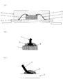
実施形態1の変形例について、図3を用いて説明する。なお、実施形態1において既に説明したコンポーネントと同様のコンポーネントについては、同様の符号を付し、その説明を省略する。
リードフレーム3は、リードフレーム3の上面において半導体チップ1の裏面と直接接続している。ここで、図3(c)は、図3(a)のリードフレーム3とボンディングワイヤ7との接合部における拡大図を示している。図3(c)に示すように、リードフレーム3は、ボンディングワイヤ7の他端とも直接接続しており、リードフレーム3とボンディングワイヤ7との接合部は、保護樹脂5により被覆されている。
樹脂封止体4は、リードフレーム3上の半導体チップ1を封止するために用いられており、図3(a)に示すように、半導体チップ1、ボンディングワイヤ7、半導体チップ1とボンディングワイヤ7との接合部、およびボンディングワイヤ7とリードフレーム3との接合部の全体を封止するように、リードフレーム3の周囲にリードフレーム3を含めて形成される。樹脂封止体4のこの他の特徴については実施形態1と同様であるため、その説明を省略する。
保護樹脂5は、半導体チップ1とボンディングワイヤ7との接合部、および、リードフレーム3とボンディングワイヤ7との接合部を被覆するために用いられている。保護樹脂5のこの他の特徴については実施形態1と同様であるため、その説明を省略する。
以上のように、半導体装置20において、半導体チップ1とボンディングワイヤ7との接合部、および、ボンディングワイヤ7とのリードフレーム3との接合部の少なくとも何れかが保護樹脂5により被覆される。これにより、ボンディングワイヤ7が予め金属により被覆されており、ワイヤボンディングの際に当該接合部において金属被膜が剥がれてしまう場合であっても、当該接合部における耐酸性および耐腐食性が向上される。また、当該両接合部を被覆する保護樹脂5は、何れも全体が樹脂封止体4により覆われるので、保護樹脂5と樹脂封止体4との界面が空気中に露出することなく、当該接合部の酸化または腐食を確実に防止することができる。以上より、半導体装置20自身の耐酸性および耐腐食性を向上させることができ、半導体装置20への信頼性を高めることができる。
(半導体装置30)
本発明に係る第2の実施形態について、図4を用いて説明する。なお、実施形態1において既に説明したコンポーネントと同様のコンポーネントについては、同様の符号を付し、その説明を省略する。
本実施形態において用いられるボンディングワイヤ7は、保護樹脂5により被覆されている。具体的には、後述のように、半導体チップ1とボンディングワイヤ7との接合部、および、ボンディング7と回路基板2との接合部が、保護樹脂5により被覆される工程(被覆工程)において、ボンディングワイヤ7も保護樹脂5により直接被覆される。それ故、本実施形態においては、半導体チップ1とボンディングワイヤ7との接合部と、ボンディングワイヤ7と、ボンディングワイヤ7と回路基板2との接合部とが、保護樹脂5により一体的に被覆される構成になっている。
以上のように、半導体装置30において、半導体チップ1とボンディングワイヤ7との接合部、および、ボンディングワイヤ7と回路基板2との接合部の少なくとも何れかが保護樹脂5により被覆される。これにより、ボンディングワイヤ7が予め金属により被覆されており、ワイヤボンディングの際に上記接合部において金属被膜が剥がれてしまう場合であっても、上記接合部における耐酸性および耐腐食性が向上される。また、当該両接合部を被覆する保護樹脂5は、何れも全体が樹脂封止体4により覆われるので、保護樹脂5と樹脂封止体4との界面が空気中に露出することなく、当該接合部の酸化または腐食を確実に防止することができる。更に、ボンディングワイヤ7自身も保護樹脂5により被覆されることにより、ボンディングワイヤ7がワイヤボンディングされてから樹脂封止体4により封止されるまでの間に酸化または腐食されることを防止することができる。以上より、半導体装置30自身の耐酸性および耐腐食性を、実施形態1に係る半導体装置10より向上させることができ、半導体装置30への信頼性より高めることができる。
(半導体装置40)
実施形態2の変形例について、図5を用いて説明する。なお、実施形態2において既に説明したコンポーネントと同様のコンポーネントについては、同様の符号を付し、その説明を省略する。
本実施形態において用いられるボンディングワイヤ7は、実施形態2と同様に、保護樹脂5により被覆されている。具体的には、後述のように、半導体チップ1とボンディングワイヤ7との接合部、および、ボンディングワイヤ7とリードフレーム3との接合部が、保護樹脂5により被覆される工程(被覆工程)において、ボンディングワイヤ7も保護樹脂5により直接被覆される。それ故、本実施形態において、半導体チップ1とボンディングワイヤ7との接合部と、ボンディングワイヤ7と、ボンディングワイヤ7とリードフレーム3との接合部とが、保護樹脂5により一体的に被覆される構成になっている。
以上のように、半導体装置40において、半導体チップ1とボンディングワイヤ7との接合部、および、ボンディングワイヤ7とリードフレーム3との接合部の少なくとも何れかが保護樹脂5により被覆される。これにより、ボンディングワイヤ7が予め金属により被覆されており、ワイヤボンディングの際に上記接合部において金属被膜が剥がれてしまう場合であっても、上記接合部における耐酸性および耐腐食性が向上される。また、当該両接合部を被覆する保護樹脂5は、何れも全体が樹脂封止体4により覆われるので、保護樹脂5と樹脂封止体4との界面が空気中に露出することなく、当該接合部の酸化または腐食を確実に防止することができる。更に、ボンディングワイヤ7自身も保護樹脂5により被覆されることにより、ボンディングワイヤ7がワイヤボンディングされてから樹脂封止体4により封止されるまでの間に酸化または腐食されることを防止することができる。以上より、半導体装置40自身の耐酸性および耐腐食性を、実施形態1に係る半導体装置10より向上させることができ、半導体装置40への信頼性より高めることができる。
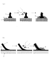
以下では、図6を参照しながら、実施形態1に係る、滴下による保護樹脂5の被覆方法について説明する。
本被覆方法において、噴射ノズル12からの保護樹脂5の滴下は、重力を用いた自然滴下により為されている。しかしながら、本被服方法においては、特にこれに限定されず、例えば、静電気力などの電気的な力を用いて滴下させてもよい。
以下では、図7を参照しながら、実施形態2に係る、噴霧による保護樹脂5の被覆方法について説明する。
本被覆方法において、(1)のワイヤボンディング工程では、ボンディングワイヤ7を半導体チップ1に接続してから回路基板2に接続しているが、これに限定されず、反対に、ボンディングワイヤ7を回路基板2に接続してから半導体チップ1に接続してもよい。
以下では、図8を参照しながら、実施形態2に係る、保護樹脂5から成るフィルムの溶解による保護樹脂5の被覆方法について説明する。
本被覆方法においては、分かり易く説明するために、半導体チップ1とボンディングワイヤ7との接合部およびボンディングワイヤ7と回路基板2との接合部の各々において、個別のフィルム状の保護樹脂5が用いられるように記載されている。しかしながら、通常、一枚のフィルム状の保護樹脂5を用いて各接合部およびボンディングワイヤ7が被覆される。本被覆方法においては、これに限定されることなく、例えば、複数の枚のフィルム状の保護樹脂5を用いて複数回に分けて被覆してもよい。
なお、本発明は、上述した実施形態に限定されるものではなく、請求項に示した範囲で種々の変更が可能であり、異なる実施形態にそれぞれ開示された技術的手段を適宜組み合わせて得られる実施形態についても、本発明の技術的範囲に含まれる。
2 回路基板
3 リードフレーム
4 樹脂封止体(封止樹脂)
5 保護樹脂
6 外部電極端子
7 ボンディングワイヤ
8 接続パッド
9 電気接点
10、20、30、40 半導体装置
11 配線
12 噴射ノズル
Claims (10)
- 少なくとも1つの半導体チップと、
上記半導体チップを搭載する載置板と、
上記半導体チップと上記載置板とを接続する金属ワイヤと、
上記半導体チップ、上記載置板上の上記半導体チップの搭載面、および、上記金属ワイヤを封止する樹脂封止体と、
を備えており、
上記金属ワイヤと上記半導体チップとの接合部、および、上記金属ワイヤと上記載置板との接合部の少なくとも何れかが、上記樹脂封止体を構成する樹脂とは異なる樹脂から成る保護樹脂により被覆されており、
上記保護樹脂の表面全体が上記樹脂封止体により覆われている、
ことを特徴とする半導体装置。 - 上記金属ワイヤの全体が、上記保護樹脂によって直接覆われている、
ことを特徴とする請求項1に記載の半導体装置。 - 上記保護樹脂が含有する塩化物イオンおよび硫化物イオンの濃度は、100ppm以下である、
ことを特徴とする請求項1または2に記載の半導体装置。 - 上記金属ワイヤは、アルミニウムであり、
上記保護樹脂のpH値は、5以上かつ7以下である、
ことを特徴とする請求項1から3の何れか1項に記載の半導体装置。 - 上記金属ワイヤは、銅であり、
上記保護樹脂のpH値は、7以上かつ11以下である、
ことを特徴とする請求項1から3の何れか1項に記載の半導体装置。 - 少なくとも1つの半導体チップと、
上記半導体チップを搭載する載置板と、
上記半導体チップと上記載置板とを接続する金属ワイヤと、
を備えている半導体装置を製造する製造方法であって、
上記金属ワイヤと上記半導体チップとの接合部、および、上記金属ワイヤと上記載置板との接合部の少なくとも何れかを保護樹脂により被覆する被覆工程と、
上記保護樹脂の表面全体を、上記保護樹脂を構成する樹脂とは異なる樹脂から成る樹脂封止体によって覆う封止工程と、
を含んでいる、
ことを特徴とする製造方法。 - 上記被覆工程において、上記保護樹脂を滴下することにより上記接合部を被覆する、
ことを特徴とする請求項6に記載の製造方法。 - 上記被覆工程において、上記金属ワイヤの全体を上記保護樹脂によって被覆する、
ことを特徴とする請求項6に記載の製造方法。 - 上記被覆工程において、上記保護樹脂を噴霧することにより被覆する、
ことを特徴とする請求項8に記載の製造方法。 - 上記被覆工程において、上記保護樹脂から成るフィルムを溶融することにより被覆する、
ことを特徴とする請求項8に記載の製造方法。
Priority Applications (1)
| Application Number | Priority Date | Filing Date | Title |
|---|---|---|---|
| JP2012066194A JP2013197531A (ja) | 2012-03-22 | 2012-03-22 | 半導体装置およびその製造方法 |
Applications Claiming Priority (1)
| Application Number | Priority Date | Filing Date | Title |
|---|---|---|---|
| JP2012066194A JP2013197531A (ja) | 2012-03-22 | 2012-03-22 | 半導体装置およびその製造方法 |
Related Child Applications (1)
| Application Number | Title | Priority Date | Filing Date |
|---|---|---|---|
| JP2016165026A Division JP2016195292A (ja) | 2016-08-25 | 2016-08-25 | 半導体装置およびその製造方法 |
Publications (2)
| Publication Number | Publication Date |
|---|---|
| JP2013197531A true JP2013197531A (ja) | 2013-09-30 |
| JP2013197531A5 JP2013197531A5 (ja) | 2014-08-28 |
Family
ID=49396066
Family Applications (1)
| Application Number | Title | Priority Date | Filing Date |
|---|---|---|---|
| JP2012066194A Pending JP2013197531A (ja) | 2012-03-22 | 2012-03-22 | 半導体装置およびその製造方法 |
Country Status (1)
| Country | Link |
|---|---|
| JP (1) | JP2013197531A (ja) |
Cited By (8)
| Publication number | Priority date | Publication date | Assignee | Title |
|---|---|---|---|---|
| KR20140145403A (ko) * | 2013-06-13 | 2014-12-23 | 엘지이노텍 주식회사 | 발광 소자 및 이를 구비한 조명 시스템 |
| EP3163610A1 (en) * | 2015-11-02 | 2017-05-03 | MediaTek Inc. | Semiconductor package with coated bonding wires |
| CN107403782A (zh) * | 2016-05-20 | 2017-11-28 | 英飞凌科技股份有限公司 | 芯片封装体、形成芯片封装体的方法和形成电接触结构的方法 |
| FR3058260A1 (fr) * | 2016-11-03 | 2018-05-04 | Stmicroelectronics (Grenoble 2) Sas | Procede de realisation d'une connexion electrique entre une puce electronique et une plaque de support et dispositif electronique |
| JP2019009171A (ja) * | 2017-06-21 | 2019-01-17 | スタンレー電気株式会社 | 半導体装置 |
| US10224306B2 (en) | 2016-11-03 | 2019-03-05 | Stmicroelectronics (Grenoble 2) Sas | Method for forming an electrical connection between an electronic chip and a carrier substrate and electronic device |
| US10847488B2 (en) | 2015-11-02 | 2020-11-24 | Mediatek Inc. | Semiconductor package having multi-tier bonding wires and components directly mounted on the multi-tier bonding wires |
| CN112292766A (zh) * | 2018-06-04 | 2021-01-29 | 雷莱昂等离子有限责任公司 | 具有电陶瓷部件的装置 |
Citations (14)
| Publication number | Priority date | Publication date | Assignee | Title |
|---|---|---|---|---|
| JPS61111569A (ja) * | 1984-11-06 | 1986-05-29 | Shin Etsu Chem Co Ltd | 樹脂封止半導体装置 |
| JPS61268464A (ja) * | 1985-05-23 | 1986-11-27 | Kyocera Corp | サ−マルプリントヘツド |
| JPS6224650A (ja) * | 1985-07-24 | 1987-02-02 | Hitachi Vlsi Eng Corp | 半導体装置 |
| JPS6297360A (ja) * | 1985-10-24 | 1987-05-06 | Mitsubishi Metal Corp | 半導体装置のボンデイングワイヤ用表面被覆高純度銅極細線 |
| JPH0582678A (ja) * | 1991-09-24 | 1993-04-02 | Sanyo Electric Co Ltd | 混成集積回路 |
| JP2001226565A (ja) * | 2000-12-25 | 2001-08-21 | Nitto Denko Corp | 半導体装置 |
| JP2003092379A (ja) * | 2001-09-18 | 2003-03-28 | Hitachi Ltd | 半導体装置 |
| JP2003261576A (ja) * | 2002-03-08 | 2003-09-19 | Shin Etsu Chem Co Ltd | 有機ケイ素化合物の精製方法及び硬化性シリコーン組成物 |
| JP2004064033A (ja) * | 2001-10-23 | 2004-02-26 | Sumitomo Electric Wintec Inc | ボンディングワイヤー |
| JP2006241411A (ja) * | 2005-03-07 | 2006-09-14 | Nitto Denko Corp | 半導体封止用エポキシ樹脂組成物およびその製法ならびにそれを用いた半導体装置 |
| JP2009263601A (ja) * | 2008-04-30 | 2009-11-12 | Hitachi Chem Co Ltd | 封止用エポキシ樹脂成形材料及び電子部品装置 |
| JP2010157695A (ja) * | 2008-12-29 | 2010-07-15 | Jin Imu Myun | チップパッケージ化における保護薄膜コーティング |
| WO2010147187A1 (ja) * | 2009-06-18 | 2010-12-23 | ローム株式会社 | 半導体装置 |
| WO2011070739A1 (ja) * | 2009-12-07 | 2011-06-16 | 住友ベークライト株式会社 | 半導体封止用エポキシ樹脂組成物、その硬化体及び半導体装置 |
-
2012
- 2012-03-22 JP JP2012066194A patent/JP2013197531A/ja active Pending
Patent Citations (14)
| Publication number | Priority date | Publication date | Assignee | Title |
|---|---|---|---|---|
| JPS61111569A (ja) * | 1984-11-06 | 1986-05-29 | Shin Etsu Chem Co Ltd | 樹脂封止半導体装置 |
| JPS61268464A (ja) * | 1985-05-23 | 1986-11-27 | Kyocera Corp | サ−マルプリントヘツド |
| JPS6224650A (ja) * | 1985-07-24 | 1987-02-02 | Hitachi Vlsi Eng Corp | 半導体装置 |
| JPS6297360A (ja) * | 1985-10-24 | 1987-05-06 | Mitsubishi Metal Corp | 半導体装置のボンデイングワイヤ用表面被覆高純度銅極細線 |
| JPH0582678A (ja) * | 1991-09-24 | 1993-04-02 | Sanyo Electric Co Ltd | 混成集積回路 |
| JP2001226565A (ja) * | 2000-12-25 | 2001-08-21 | Nitto Denko Corp | 半導体装置 |
| JP2003092379A (ja) * | 2001-09-18 | 2003-03-28 | Hitachi Ltd | 半導体装置 |
| JP2004064033A (ja) * | 2001-10-23 | 2004-02-26 | Sumitomo Electric Wintec Inc | ボンディングワイヤー |
| JP2003261576A (ja) * | 2002-03-08 | 2003-09-19 | Shin Etsu Chem Co Ltd | 有機ケイ素化合物の精製方法及び硬化性シリコーン組成物 |
| JP2006241411A (ja) * | 2005-03-07 | 2006-09-14 | Nitto Denko Corp | 半導体封止用エポキシ樹脂組成物およびその製法ならびにそれを用いた半導体装置 |
| JP2009263601A (ja) * | 2008-04-30 | 2009-11-12 | Hitachi Chem Co Ltd | 封止用エポキシ樹脂成形材料及び電子部品装置 |
| JP2010157695A (ja) * | 2008-12-29 | 2010-07-15 | Jin Imu Myun | チップパッケージ化における保護薄膜コーティング |
| WO2010147187A1 (ja) * | 2009-06-18 | 2010-12-23 | ローム株式会社 | 半導体装置 |
| WO2011070739A1 (ja) * | 2009-12-07 | 2011-06-16 | 住友ベークライト株式会社 | 半導体封止用エポキシ樹脂組成物、その硬化体及び半導体装置 |
Cited By (20)
| Publication number | Priority date | Publication date | Assignee | Title |
|---|---|---|---|---|
| KR20140145403A (ko) * | 2013-06-13 | 2014-12-23 | 엘지이노텍 주식회사 | 발광 소자 및 이를 구비한 조명 시스템 |
| KR102063508B1 (ko) | 2013-06-13 | 2020-01-08 | 엘지이노텍 주식회사 | 발광 소자 및 이를 구비한 조명 시스템 |
| EP3163610A1 (en) * | 2015-11-02 | 2017-05-03 | MediaTek Inc. | Semiconductor package with coated bonding wires |
| CN106941098A (zh) * | 2015-11-02 | 2017-07-11 | 联发科技股份有限公司 | 半导体封装及其制造方法 |
| US11257780B2 (en) | 2015-11-02 | 2022-02-22 | Mediatek Inc. | Semiconductor package having multi-tier bonding wires and components directly mounted on the multi-tier bonding wires |
| US10847488B2 (en) | 2015-11-02 | 2020-11-24 | Mediatek Inc. | Semiconductor package having multi-tier bonding wires and components directly mounted on the multi-tier bonding wires |
| US10037936B2 (en) | 2015-11-02 | 2018-07-31 | Mediatek Inc. | Semiconductor package with coated bonding wires and fabrication method thereof |
| US10461056B2 (en) | 2016-05-20 | 2019-10-29 | Infineon Technologies Ag | Chip package and method of forming a chip package with a metal contact structure and protective layer, and method of forming an electrical contact |
| CN107403782A (zh) * | 2016-05-20 | 2017-11-28 | 英飞凌科技股份有限公司 | 芯片封装体、形成芯片封装体的方法和形成电接触结构的方法 |
| EP3319115A1 (fr) * | 2016-11-03 | 2018-05-09 | STMicroelectronics (Grenoble 2) SAS | Procédé de réalisation d'une connexion électrique entre une puce électronique et une plaque de support et dispositif électronique |
| US10224306B2 (en) | 2016-11-03 | 2019-03-05 | Stmicroelectronics (Grenoble 2) Sas | Method for forming an electrical connection between an electronic chip and a carrier substrate and electronic device |
| US10643970B2 (en) | 2016-11-03 | 2020-05-05 | Stmicroelectronics (Grenoble 2) Sas | Method for forming an electrical connection between an electronic chip and a carrier substrate and electronic device |
| CN108022908A (zh) * | 2016-11-03 | 2018-05-11 | 意法半导体(格勒诺布尔2)公司 | 用于形成电连接的方法和电子器件 |
| FR3058260A1 (fr) * | 2016-11-03 | 2018-05-04 | Stmicroelectronics (Grenoble 2) Sas | Procede de realisation d'une connexion electrique entre une puce electronique et une plaque de support et dispositif electronique |
| US11557566B2 (en) | 2016-11-03 | 2023-01-17 | Stmicroelectronics (Grenoble 2) Sas | Method for forming an electrical connection between an electronic chip and a carrier substrate and electronic device |
| JP2019009171A (ja) * | 2017-06-21 | 2019-01-17 | スタンレー電気株式会社 | 半導体装置 |
| JP7096649B2 (ja) | 2017-06-21 | 2022-07-06 | スタンレー電気株式会社 | 半導体装置 |
| CN112292766A (zh) * | 2018-06-04 | 2021-01-29 | 雷莱昂等离子有限责任公司 | 具有电陶瓷部件的装置 |
| JP2021526731A (ja) * | 2018-06-04 | 2021-10-07 | レリオン プラズマ ゲーエムベーハー | エレクトロセラミック部材を有する装置 |
| JP7402825B2 (ja) | 2018-06-04 | 2023-12-21 | レリオン プラズマ ゲーエムベーハー | エレクトロセラミック部材を有する装置 |
Similar Documents
| Publication | Publication Date | Title |
|---|---|---|
| JP2013197531A (ja) | 半導体装置およびその製造方法 | |
| JP2013197531A5 (ja) | ||
| US10825755B2 (en) | Method of forming a packaged semiconductor device having enhanced wettable flank and structure | |
| JP3602453B2 (ja) | 半導体装置 | |
| US20090108445A1 (en) | Substrate structure and semiconductor package using the same | |
| US9478517B2 (en) | Electronic device package structure and method of fabricating the same | |
| US7329944B2 (en) | Leadframe for semiconductor device | |
| JP4967701B2 (ja) | 電力半導体装置 | |
| JP2009071156A (ja) | 半導体装置及びその製造方法 | |
| US20120119358A1 (en) | Semicondiuctor package substrate and method for manufacturing the same | |
| JP2016195292A (ja) | 半導体装置およびその製造方法 | |
| JP6109078B2 (ja) | リードクラックが強化された電子素子用テープ | |
| JP2011249599A (ja) | 半導体実装基板およびそれを用いた実装構造体 | |
| CN101625986A (zh) | 芯片封装结构制程 | |
| CN103165558B (zh) | 封装结构及其制造方法 | |
| JP3964319B2 (ja) | 半導体装置 | |
| JP2003068965A (ja) | 半導体装置 | |
| CN104981092A (zh) | 表面镀层和包括该表面镀层的半导体封装件 | |
| US6420210B2 (en) | Semiconductor device and method for manufacturing the same | |
| WO2015129185A1 (ja) | 樹脂封止型半導体装置、およびその製造方法、ならびにその実装体 | |
| JP2005217082A (ja) | 半導体実装体 | |
| JP2775262B2 (ja) | 電子部品搭載用基板及び電子部品搭載装置 | |
| JP4844735B2 (ja) | 半導体装置の製造方法 | |
| US9123699B1 (en) | Formation of package pins in semiconductor packaging | |
| KR100585585B1 (ko) | 반도체 패키지 |
Legal Events
| Date | Code | Title | Description |
|---|---|---|---|
| A521 | Written amendment |
Free format text: JAPANESE INTERMEDIATE CODE: A523 Effective date: 20140710 |
|
| A621 | Written request for application examination |
Free format text: JAPANESE INTERMEDIATE CODE: A621 Effective date: 20140710 |
|
| A977 | Report on retrieval |
Free format text: JAPANESE INTERMEDIATE CODE: A971007 Effective date: 20150624 |
|
| A131 | Notification of reasons for refusal |
Free format text: JAPANESE INTERMEDIATE CODE: A131 Effective date: 20150707 |
|
| A521 | Written amendment |
Free format text: JAPANESE INTERMEDIATE CODE: A523 Effective date: 20150902 |
|
| A131 | Notification of reasons for refusal |
Free format text: JAPANESE INTERMEDIATE CODE: A131 Effective date: 20160209 |
|
| A02 | Decision of refusal |
Free format text: JAPANESE INTERMEDIATE CODE: A02 Effective date: 20160823 |