JP2012216454A - Light-emitting device and electronic apparatus - Google Patents
Light-emitting device and electronic apparatus Download PDFInfo
- Publication number
- JP2012216454A JP2012216454A JP2011081639A JP2011081639A JP2012216454A JP 2012216454 A JP2012216454 A JP 2012216454A JP 2011081639 A JP2011081639 A JP 2011081639A JP 2011081639 A JP2011081639 A JP 2011081639A JP 2012216454 A JP2012216454 A JP 2012216454A
- Authority
- JP
- Japan
- Prior art keywords
- layer
- light emitting
- emitting device
- microlens
- light
- Prior art date
- Legal status (The legal status is an assumption and is not a legal conclusion. Google has not performed a legal analysis and makes no representation as to the accuracy of the status listed.)
- Withdrawn
Links
- 238000007789 sealing Methods 0.000 claims abstract description 61
- 239000000758 substrate Substances 0.000 claims abstract description 39
- 229920005989 resin Polymers 0.000 claims description 12
- 239000011347 resin Substances 0.000 claims description 12
- VYPSYNLAJGMNEJ-UHFFFAOYSA-N Silicium dioxide Chemical class O=[Si]=O VYPSYNLAJGMNEJ-UHFFFAOYSA-N 0.000 claims description 11
- 229910052814 silicon oxide Inorganic materials 0.000 claims description 11
- 230000000630 rising effect Effects 0.000 claims description 6
- 229910052581 Si3N4 Inorganic materials 0.000 claims description 5
- XUIMIQQOPSSXEZ-UHFFFAOYSA-N Silicon Chemical compound [Si] XUIMIQQOPSSXEZ-UHFFFAOYSA-N 0.000 claims description 5
- 229910052710 silicon Inorganic materials 0.000 claims description 5
- 239000010703 silicon Substances 0.000 claims description 5
- HQVNEWCFYHHQES-UHFFFAOYSA-N silicon nitride Chemical compound N12[Si]34N5[Si]62N3[Si]51N64 HQVNEWCFYHHQES-UHFFFAOYSA-N 0.000 claims description 5
- YCKRFDGAMUMZLT-UHFFFAOYSA-N Fluorine atom Chemical compound [F] YCKRFDGAMUMZLT-UHFFFAOYSA-N 0.000 claims description 4
- 239000011737 fluorine Substances 0.000 claims description 4
- 229910052731 fluorine Inorganic materials 0.000 claims description 4
- 239000002105 nanoparticle Substances 0.000 claims description 4
- TWNQGVIAIRXVLR-UHFFFAOYSA-N oxo(oxoalumanyloxy)alumane Chemical compound O=[Al]O[Al]=O TWNQGVIAIRXVLR-UHFFFAOYSA-N 0.000 claims description 4
- 238000000605 extraction Methods 0.000 abstract description 12
- 230000035699 permeability Effects 0.000 abstract description 7
- 230000006872 improvement Effects 0.000 abstract description 4
- 239000010410 layer Substances 0.000 description 93
- 239000010408 film Substances 0.000 description 62
- 239000000463 material Substances 0.000 description 20
- 238000000034 method Methods 0.000 description 17
- 230000002093 peripheral effect Effects 0.000 description 13
- 239000004593 Epoxy Substances 0.000 description 11
- 238000005192 partition Methods 0.000 description 10
- 238000001723 curing Methods 0.000 description 9
- -1 lithium oxide Chemical compound 0.000 description 9
- 238000011049 filling Methods 0.000 description 8
- 230000004888 barrier function Effects 0.000 description 7
- 239000011368 organic material Substances 0.000 description 7
- 239000000178 monomer Substances 0.000 description 6
- 239000002245 particle Substances 0.000 description 6
- 239000011159 matrix material Substances 0.000 description 5
- 229910052751 metal Inorganic materials 0.000 description 5
- 239000002184 metal Substances 0.000 description 5
- 238000002156 mixing Methods 0.000 description 5
- 238000002834 transmittance Methods 0.000 description 5
- QVGXLLKOCUKJST-UHFFFAOYSA-N atomic oxygen Chemical compound [O] QVGXLLKOCUKJST-UHFFFAOYSA-N 0.000 description 4
- IISBACLAFKSPIT-UHFFFAOYSA-N bisphenol A Chemical compound C=1C=C(O)C=CC=1C(C)(C)C1=CC=C(O)C=C1 IISBACLAFKSPIT-UHFFFAOYSA-N 0.000 description 4
- PXKLMJQFEQBVLD-UHFFFAOYSA-N bisphenol F Chemical compound C1=CC(O)=CC=C1CC1=CC=C(O)C=C1 PXKLMJQFEQBVLD-UHFFFAOYSA-N 0.000 description 4
- 239000003990 capacitor Substances 0.000 description 4
- 238000000576 coating method Methods 0.000 description 4
- VYFYYTLLBUKUHU-UHFFFAOYSA-N dopamine Chemical compound NCCC1=CC=C(O)C(O)=C1 VYFYYTLLBUKUHU-UHFFFAOYSA-N 0.000 description 4
- 230000000694 effects Effects 0.000 description 4
- 238000007689 inspection Methods 0.000 description 4
- 238000004519 manufacturing process Methods 0.000 description 4
- 239000001301 oxygen Substances 0.000 description 4
- 229910052760 oxygen Inorganic materials 0.000 description 4
- 239000012798 spherical particle Substances 0.000 description 4
- XLYOFNOQVPJJNP-UHFFFAOYSA-N water Substances O XLYOFNOQVPJJNP-UHFFFAOYSA-N 0.000 description 4
- 239000004925 Acrylic resin Substances 0.000 description 3
- 229920000178 Acrylic resin Polymers 0.000 description 3
- 239000012790 adhesive layer Substances 0.000 description 3
- 229910052782 aluminium Inorganic materials 0.000 description 3
- XAGFODPZIPBFFR-UHFFFAOYSA-N aluminium Chemical compound [Al] XAGFODPZIPBFFR-UHFFFAOYSA-N 0.000 description 3
- 239000003795 chemical substances by application Substances 0.000 description 3
- 238000010586 diagram Methods 0.000 description 3
- 230000010365 information processing Effects 0.000 description 3
- 238000002347 injection Methods 0.000 description 3
- 239000007924 injection Substances 0.000 description 3
- LIVNPJMFVYWSIS-UHFFFAOYSA-N silicon monoxide Chemical group [Si-]#[O+] LIVNPJMFVYWSIS-UHFFFAOYSA-N 0.000 description 3
- UWRZIZXBOLBCON-VOTSOKGWSA-N (e)-2-phenylethenamine Chemical compound N\C=C\C1=CC=CC=C1 UWRZIZXBOLBCON-VOTSOKGWSA-N 0.000 description 2
- AOBIOSPNXBMOAT-UHFFFAOYSA-N 2-[2-(oxiran-2-ylmethoxy)ethoxymethyl]oxirane Chemical compound C1OC1COCCOCC1CO1 AOBIOSPNXBMOAT-UHFFFAOYSA-N 0.000 description 2
- OYPRJOBELJOOCE-UHFFFAOYSA-N Calcium Chemical compound [Ca] OYPRJOBELJOOCE-UHFFFAOYSA-N 0.000 description 2
- ISWSIDIOOBJBQZ-UHFFFAOYSA-N Phenol Chemical compound OC1=CC=CC=C1 ISWSIDIOOBJBQZ-UHFFFAOYSA-N 0.000 description 2
- 239000002202 Polyethylene glycol Substances 0.000 description 2
- XLOMVQKBTHCTTD-UHFFFAOYSA-N Zinc monoxide Chemical compound [Zn]=O XLOMVQKBTHCTTD-UHFFFAOYSA-N 0.000 description 2
- 150000008065 acid anhydrides Chemical class 0.000 description 2
- MWPLVEDNUUSJAV-UHFFFAOYSA-N anthracene Chemical compound C1=CC=CC2=CC3=CC=CC=C3C=C21 MWPLVEDNUUSJAV-UHFFFAOYSA-N 0.000 description 2
- 229910052791 calcium Inorganic materials 0.000 description 2
- 239000011575 calcium Substances 0.000 description 2
- 239000003086 colorant Substances 0.000 description 2
- 239000004020 conductor Substances 0.000 description 2
- 230000007547 defect Effects 0.000 description 2
- 229960003638 dopamine Drugs 0.000 description 2
- 125000003700 epoxy group Chemical group 0.000 description 2
- 239000007789 gas Substances 0.000 description 2
- PQXKHYXIUOZZFA-UHFFFAOYSA-M lithium fluoride Chemical compound [Li+].[F-] PQXKHYXIUOZZFA-UHFFFAOYSA-M 0.000 description 2
- 150000002736 metal compounds Chemical class 0.000 description 2
- 229910044991 metal oxide Inorganic materials 0.000 description 2
- 150000004706 metal oxides Chemical class 0.000 description 2
- 239000000203 mixture Substances 0.000 description 2
- 229920003986 novolac Polymers 0.000 description 2
- 150000002894 organic compounds Chemical class 0.000 description 2
- 238000000059 patterning Methods 0.000 description 2
- 238000000206 photolithography Methods 0.000 description 2
- 229920001223 polyethylene glycol Polymers 0.000 description 2
- 229920000642 polymer Polymers 0.000 description 2
- 230000008569 process Effects 0.000 description 2
- 150000003377 silicon compounds Chemical class 0.000 description 2
- 239000002356 single layer Substances 0.000 description 2
- 239000010409 thin film Substances 0.000 description 2
- CDAWCLOXVUBKRW-UHFFFAOYSA-N 2-aminophenol Chemical compound NC1=CC=CC=C1O CDAWCLOXVUBKRW-UHFFFAOYSA-N 0.000 description 1
- XPEKVUUBSDFMDR-UHFFFAOYSA-N 4-methyl-3a,4,7,7a-tetrahydro-2-benzofuran-1,3-dione Chemical compound CC1C=CCC2C(=O)OC(=O)C12 XPEKVUUBSDFMDR-UHFFFAOYSA-N 0.000 description 1
- VQVIHDPBMFABCQ-UHFFFAOYSA-N 5-(1,3-dioxo-2-benzofuran-5-carbonyl)-2-benzofuran-1,3-dione Chemical compound C1=C2C(=O)OC(=O)C2=CC(C(C=2C=C3C(=O)OC(=O)C3=CC=2)=O)=C1 VQVIHDPBMFABCQ-UHFFFAOYSA-N 0.000 description 1
- 229910001316 Ag alloy Inorganic materials 0.000 description 1
- 229910000838 Al alloy Inorganic materials 0.000 description 1
- RYGMFSIKBFXOCR-UHFFFAOYSA-N Copper Chemical compound [Cu] RYGMFSIKBFXOCR-UHFFFAOYSA-N 0.000 description 1
- LFQSCWFLJHTTHZ-UHFFFAOYSA-N Ethanol Chemical compound CCO LFQSCWFLJHTTHZ-UHFFFAOYSA-N 0.000 description 1
- DGAQECJNVWCQMB-PUAWFVPOSA-M Ilexoside XXIX Chemical compound C[C@@H]1CC[C@@]2(CC[C@@]3(C(=CC[C@H]4[C@]3(CC[C@@H]5[C@@]4(CC[C@@H](C5(C)C)OS(=O)(=O)[O-])C)C)[C@@H]2[C@]1(C)O)C)C(=O)O[C@H]6[C@@H]([C@H]([C@@H]([C@H](O6)CO)O)O)O.[Na+] DGAQECJNVWCQMB-PUAWFVPOSA-M 0.000 description 1
- FYYHWMGAXLPEAU-UHFFFAOYSA-N Magnesium Chemical compound [Mg] FYYHWMGAXLPEAU-UHFFFAOYSA-N 0.000 description 1
- BQCADISMDOOEFD-UHFFFAOYSA-N Silver Chemical compound [Ag] BQCADISMDOOEFD-UHFFFAOYSA-N 0.000 description 1
- GWEVSGVZZGPLCZ-UHFFFAOYSA-N Titan oxide Chemical compound O=[Ti]=O GWEVSGVZZGPLCZ-UHFFFAOYSA-N 0.000 description 1
- GTDPSWPPOUPBNX-UHFFFAOYSA-N ac1mqpva Chemical compound CC12C(=O)OC(=O)C1(C)C1(C)C2(C)C(=O)OC1=O GTDPSWPPOUPBNX-UHFFFAOYSA-N 0.000 description 1
- 125000005595 acetylacetonate group Chemical group 0.000 description 1
- 238000012644 addition polymerization Methods 0.000 description 1
- 238000000149 argon plasma sintering Methods 0.000 description 1
- 150000004982 aromatic amines Chemical class 0.000 description 1
- 230000008901 benefit Effects 0.000 description 1
- UHOVQNZJYSORNB-UHFFFAOYSA-N benzene Substances C1=CC=CC=C1 UHOVQNZJYSORNB-UHFFFAOYSA-N 0.000 description 1
- 230000003139 buffering effect Effects 0.000 description 1
- WUKWITHWXAAZEY-UHFFFAOYSA-L calcium difluoride Chemical compound [F-].[F-].[Ca+2] WUKWITHWXAAZEY-UHFFFAOYSA-L 0.000 description 1
- 229910001634 calcium fluoride Inorganic materials 0.000 description 1
- 238000010538 cationic polymerization reaction Methods 0.000 description 1
- 239000011248 coating agent Substances 0.000 description 1
- 229910052802 copper Inorganic materials 0.000 description 1
- 239000010949 copper Substances 0.000 description 1
- 230000007423 decrease Effects 0.000 description 1
- 239000012954 diazonium Substances 0.000 description 1
- 150000001989 diazonium salts Chemical class 0.000 description 1
- OZLBDYMWFAHSOQ-UHFFFAOYSA-N diphenyliodanium Chemical class C=1C=CC=CC=1[I+]C1=CC=CC=C1 OZLBDYMWFAHSOQ-UHFFFAOYSA-N 0.000 description 1
- 238000010292 electrical insulation Methods 0.000 description 1
- 239000003822 epoxy resin Substances 0.000 description 1
- 239000000284 extract Substances 0.000 description 1
- 239000000945 filler Substances 0.000 description 1
- 239000011521 glass Substances 0.000 description 1
- PCHJSUWPFVWCPO-UHFFFAOYSA-N gold Chemical compound [Au] PCHJSUWPFVWCPO-UHFFFAOYSA-N 0.000 description 1
- 229910052737 gold Inorganic materials 0.000 description 1
- 239000010931 gold Substances 0.000 description 1
- 238000010438 heat treatment Methods 0.000 description 1
- 230000005525 hole transport Effects 0.000 description 1
- 230000001771 impaired effect Effects 0.000 description 1
- 229910052738 indium Inorganic materials 0.000 description 1
- APFVFJFRJDLVQX-UHFFFAOYSA-N indium atom Chemical compound [In] APFVFJFRJDLVQX-UHFFFAOYSA-N 0.000 description 1
- 229910003437 indium oxide Inorganic materials 0.000 description 1
- PJXISJQVUVHSOJ-UHFFFAOYSA-N indium(iii) oxide Chemical compound [O-2].[O-2].[O-2].[In+3].[In+3] PJXISJQVUVHSOJ-UHFFFAOYSA-N 0.000 description 1
- 239000003999 initiator Substances 0.000 description 1
- 229910010272 inorganic material Inorganic materials 0.000 description 1
- 239000011147 inorganic material Substances 0.000 description 1
- XEEYBQQBJWHFJM-UHFFFAOYSA-N iron Substances [Fe] XEEYBQQBJWHFJM-UHFFFAOYSA-N 0.000 description 1
- 229910052742 iron Inorganic materials 0.000 description 1
- 239000004973 liquid crystal related substance Substances 0.000 description 1
- 229910052744 lithium Inorganic materials 0.000 description 1
- FUJCRWPEOMXPAD-UHFFFAOYSA-N lithium oxide Chemical compound [Li+].[Li+].[O-2] FUJCRWPEOMXPAD-UHFFFAOYSA-N 0.000 description 1
- 229910001947 lithium oxide Inorganic materials 0.000 description 1
- 229910052749 magnesium Inorganic materials 0.000 description 1
- 239000011777 magnesium Substances 0.000 description 1
- SJCKRGFTWFGHGZ-UHFFFAOYSA-N magnesium silver Chemical compound [Mg].[Ag] SJCKRGFTWFGHGZ-UHFFFAOYSA-N 0.000 description 1
- 239000012528 membrane Substances 0.000 description 1
- 229910001512 metal fluoride Inorganic materials 0.000 description 1
- 150000002739 metals Chemical class 0.000 description 1
- DCZNSJVFOQPSRV-UHFFFAOYSA-N n,n-diphenyl-4-[4-(n-phenylanilino)phenyl]aniline Chemical compound C1=CC=CC=C1N(C=1C=CC(=CC=1)C=1C=CC(=CC=1)N(C=1C=CC=CC=1)C=1C=CC=CC=1)C1=CC=CC=C1 DCZNSJVFOQPSRV-UHFFFAOYSA-N 0.000 description 1
- 230000003287 optical effect Effects 0.000 description 1
- 125000002524 organometallic group Chemical group 0.000 description 1
- 238000010422 painting Methods 0.000 description 1
- 229920003023 plastic Polymers 0.000 description 1
- 229920000515 polycarbonate Polymers 0.000 description 1
- 239000004417 polycarbonate Substances 0.000 description 1
- 229920000647 polyepoxide Polymers 0.000 description 1
- 239000005020 polyethylene terephthalate Substances 0.000 description 1
- 229920000139 polyethylene terephthalate Polymers 0.000 description 1
- 229920000098 polyolefin Polymers 0.000 description 1
- 239000002994 raw material Substances 0.000 description 1
- 238000012827 research and development Methods 0.000 description 1
- 230000004044 response Effects 0.000 description 1
- 238000007142 ring opening reaction Methods 0.000 description 1
- YYMBJDOZVAITBP-UHFFFAOYSA-N rubrene Chemical compound C1=CC=CC=C1C(C1=C(C=2C=CC=CC=2)C2=CC=CC=C2C(C=2C=CC=CC=2)=C11)=C(C=CC=C2)C2=C1C1=CC=CC=C1 YYMBJDOZVAITBP-UHFFFAOYSA-N 0.000 description 1
- 150000003839 salts Chemical class 0.000 description 1
- 239000000565 sealant Substances 0.000 description 1
- SCPYDCQAZCOKTP-UHFFFAOYSA-N silanol Chemical compound [SiH3]O SCPYDCQAZCOKTP-UHFFFAOYSA-N 0.000 description 1
- 229910052709 silver Inorganic materials 0.000 description 1
- 239000004332 silver Substances 0.000 description 1
- 229910052708 sodium Inorganic materials 0.000 description 1
- 239000011734 sodium Substances 0.000 description 1
- 239000002904 solvent Substances 0.000 description 1
- 238000000638 solvent extraction Methods 0.000 description 1
- 238000004528 spin coating Methods 0.000 description 1
- 125000006158 tetracarboxylic acid group Chemical group 0.000 description 1
- 229920001187 thermosetting polymer Polymers 0.000 description 1
- XOLBLPGZBRYERU-UHFFFAOYSA-N tin dioxide Chemical compound O=[Sn]=O XOLBLPGZBRYERU-UHFFFAOYSA-N 0.000 description 1
- 229910001887 tin oxide Inorganic materials 0.000 description 1
- OGIDPMRJRNCKJF-UHFFFAOYSA-N titanium oxide Inorganic materials [Ti]=O OGIDPMRJRNCKJF-UHFFFAOYSA-N 0.000 description 1
- TVIVIEFSHFOWTE-UHFFFAOYSA-K tri(quinolin-8-yloxy)alumane Chemical compound [Al+3].C1=CN=C2C([O-])=CC=CC2=C1.C1=CN=C2C([O-])=CC=CC2=C1.C1=CN=C2C([O-])=CC=CC2=C1 TVIVIEFSHFOWTE-UHFFFAOYSA-K 0.000 description 1
- 125000005259 triarylamine group Chemical group 0.000 description 1
- 238000001771 vacuum deposition Methods 0.000 description 1
- YVTHLONGBIQYBO-UHFFFAOYSA-N zinc indium(3+) oxygen(2-) Chemical compound [O--].[Zn++].[In+3] YVTHLONGBIQYBO-UHFFFAOYSA-N 0.000 description 1
- 239000011787 zinc oxide Substances 0.000 description 1
Images


Abstract
Description
本発明は、発光装置および当該発光装置を備えた電子機器に関する。 The present invention relates to a light emitting device and an electronic apparatus including the light emitting device.
近年、自発光素子である有機EL素子を画素として用いた有機EL装置の開発が進められている。有機EL装置は、高輝度、低消費電力で高速応答が可能であり、有機化合物の多様性により多色化が容易であると考えられることから、フルカラーディスプレイ等への応用が期待され、盛んに研究開発が行なわれている。 In recent years, organic EL devices using organic EL elements, which are self-luminous elements, as pixels have been developed. Organic EL devices are capable of high-speed response with high brightness and low power consumption, and are considered to be multicolored easily due to the variety of organic compounds. Research and development is in progress.
フルカラーディスプレイの作製に必要な3原色を得る方法としては、白色発光層とカラーフィルターとを組み合わせる方法(カラーフィルター方式;特許文献1参照)、3原色の発光層を個別に塗り分ける方法(塗り分け方式)等が提案されている。
そのうち、カラーフィルター方式は、塗り分け方式に比べると発光層の塗り分けが不要であり、白色発光層をパネル一面に形成することができることから、プロセス的には容易となる。他方、カラーフィルター方式は、光の利用効率が低く、十分な明るさが得られないという問題がある。そのため、有機EL素子の光取り出し効率を上げるために様々な取り組みが行われてきている。
As a method for obtaining the three primary colors necessary for the production of a full color display, a method of combining a white light emitting layer and a color filter (color filter method; see Patent Document 1), a method of separately coating the light emitting layers of the three primary colors (painting separately) Etc.) have been proposed.
Among them, the color filter method does not require separate application of the light emitting layer as compared with the separate application method, and the white light emitting layer can be formed on the entire surface of the panel. On the other hand, the color filter method has a problem that the light use efficiency is low and sufficient brightness cannot be obtained. Therefore, various efforts have been made to increase the light extraction efficiency of the organic EL element.
例えば、特許文献2では、マイクロレンズアレイを設置し、光取り出し効率を向上させる構造が提案されている。特許文献2の有機EL装置では、1層の封止膜上にマイクロレンズアレイが形成されている。有機発光層より発した光が空気層との界面にマイクロレンズアレイを形成することにより、空気層との界面での反射が抑えられ、光取り出し効率が向上するといった報告がなされている。 For example, Patent Document 2 proposes a structure in which a microlens array is installed to improve light extraction efficiency. In the organic EL device of Patent Document 2, a microlens array is formed on a single sealing film. It has been reported that the light emitted from the organic light emitting layer forms a microlens array at the interface with the air layer, thereby suppressing reflection at the interface with the air layer and improving the light extraction efficiency.
しかしながら、特許文献2に示す構造では、マイクロレンズアレイ上は中空構造にしないとならないため、その後、直接カラーフィルター層を形成することは困難であるという課題があった。
また、カラーフィルターを設置した後にマイクロレンズアレイを設置する構造も考えられるが、通常、隣り合うカラーフィルターに入った光が空気層との界面で全反射されるのに対し、マイクロレンズアレイにより光が取り出されてしまい、広視野角で混色が発生してしまうという課題があった。
However, the structure shown in Patent Document 2 has a problem in that it is difficult to directly form a color filter layer after that because the microlens array must have a hollow structure.
A structure in which the microlens array is installed after the color filter is installed is also conceivable. Normally, the light entering the adjacent color filter is totally reflected at the interface with the air layer, whereas the light is transmitted by the microlens array. Is taken out and color mixing occurs at a wide viewing angle.
また、特許文献2での封止性能について考えてみると、1層の封止膜だけでは、異物や画素隔壁層による段差などにより部分的にクラックが入りやすく、完全なるバリア性を有することが困難である。
これを回避するために封止膜を重ねた封止構造を採用することも考えられるが、この構造上にマイクロレンズアレイを設置し、その上部にカラーフィルターを設置する構造では、発光素子からマイクロレンズアレイまでの距離が離れるために、隣り合うマイクロレンズアレイに入った光が隣り合うカラーフィルターを通して空気層に取り出されてしまうという課題があった。
Further, considering the sealing performance in Patent Document 2, it is possible that a single layer of sealing film is easily cracked partially due to a foreign matter or a step due to a pixel partition layer, and has a complete barrier property. Have difficulty.
In order to avoid this, it is conceivable to adopt a sealing structure in which sealing films are stacked. However, in a structure in which a microlens array is installed on this structure and a color filter is installed on top of the structure, a microlens array is placed on top of the light emitting element. Since the distance to the lens array is increased, there is a problem that light entering the adjacent microlens array is extracted to the air layer through the adjacent color filter.
本発明は、上述の課題の少なくとも一部を解決するためになされたものであり、以下の形態または適用例として実現することが可能である。 SUMMARY An advantage of some aspects of the invention is to solve at least a part of the problems described above, and the invention can be implemented as the following forms or application examples.
[適用例1]本適用例の発光装置は、基板と前記基板上に形成された有機発光層を含む複数の画素と、前記複数の画素を覆う封止膜と、前記封止膜を介して前記画素を覆うマイクロレンズと、複数の前記マイクロレンズ覆う平坦化層と、前記平坦化層上において前記画素ごとに形成されたカラーフィルターと、を備え、前記マイクロレンズの屈折率が、前記平坦化層の屈折率よりも大きいことを特徴とする。 Application Example 1 A light-emitting device according to this application example includes a substrate, a plurality of pixels including an organic light-emitting layer formed on the substrate, a sealing film covering the plurality of pixels, and the sealing film interposed therebetween. A microlens covering the pixel, a plurality of planarizing layers covering the microlens, and a color filter formed for each pixel on the planarizing layer, wherein the refractive index of the microlens is the planarization It is characterized by being larger than the refractive index of the layer.
本適用例によれば、マイクロレンズが有機発光層とカラーフィルターの間に設置され、かつマイクロレンズと有機発光層との距離を非常に近接させることができるため、有機発光層で発光された光が、マイクロレンズにより集光され、その後、カラーフィルターを通過することができる。その結果、広視野角で混色が生じ難く光取り出し効率を向上させた発光装置を提供することができる。 According to this application example, since the microlens is installed between the organic light emitting layer and the color filter and the distance between the microlens and the organic light emitting layer can be made very close, the light emitted from the organic light emitting layer Can be collected by the microlens and then pass through the color filter. As a result, it is possible to provide a light emitting device in which color mixing is difficult to occur at a wide viewing angle and light extraction efficiency is improved.
[適用例2]上記適用例に記載の発光装置において、前記マイクロレンズの屈折率が1.6以上1.9以下を満たし、前記平坦化層の屈折率が1.2以上1.5以下で形成されていることを特徴とする。 Application Example 2 In the light emitting device according to the application example described above, the microlens has a refractive index of 1.6 to 1.9, and the planarization layer has a refractive index of 1.2 to 1.5. It is formed.
本適用例によれば、マイクロレンズと平坦化層との間に屈折率差が発生するため、有機発光層で発光された光が、マイクロレンズを透過する際に、正面方向に集光され、その結果、正面方向の光取り出し効率を向上させることができる。 According to this application example, since a refractive index difference occurs between the microlens and the planarization layer, the light emitted from the organic light emitting layer is condensed in the front direction when passing through the microlens, As a result, the light extraction efficiency in the front direction can be improved.
[適用例3]上記適用例に記載の発光装置において、前記平坦化層がSiO(酸化シリコン)を骨格とした無機膜あるいは有機膜と前記無機膜のハイブリッド膜であることを特徴とする。 Application Example 3 In the light emitting device according to the application example described above, the planarization layer is an inorganic film having a SiO (silicon oxide) skeleton or a hybrid film of an organic film and the inorganic film.
本適用例によれば、平坦化層にSiO(酸化シリコン)を骨格とした無機膜あるいは有機膜と無機膜のハイブリッド膜を用いるため、上記屈折率が1.5以下を実現し、かつ有機平坦化膜に比べ、水分や酸素に対するバリア性が高い膜を用いるため、光取り出し向上と低透湿性の両立を可能とする。 According to this application example, an inorganic film having a skeleton of SiO (silicon oxide) or a hybrid film of an organic film and an inorganic film is used for the flattening layer. Since a film having a high barrier property against moisture and oxygen is used as compared with the oxidized film, it is possible to achieve both improvement of light extraction and low moisture permeability.
[適用例4]上記適用例に記載の発光装置において、前記マイクロレンズがフッ素系の樹脂であること特徴とする。 Application Example 4 In the light-emitting device described in the application example, the microlens is a fluorine-based resin.
本適用例によれば、マイクロレンズにフッ素系の樹脂を用いることにより、アクリル樹脂やエポキシ樹脂に比べ、高い屈折率となるため、上記マイクロレンズの屈折率が1.6以上を得ることが可能となる。 According to this application example, by using a fluorine-based resin for the microlens, the refractive index of the microlens can be 1.6 or more because the refractive index is higher than that of acrylic resin or epoxy resin. It becomes.
[適用例5]上記適用例に記載の発光装置において、マイクロレンズが無機のナノ粒子を混入した樹脂であること特徴とする。 Application Example 5 In the light emitting device according to the application example described above, the microlens is a resin mixed with inorganic nanoparticles.
本適用例によれば、無機のナノ粒子を混入した樹脂を用いることにより、可視光波長より小さい粒子であるため、光散乱や光線透過率を損なうことなく、屈折率を上げることができるため、上記マイクロレンズの屈折率が1.6以上を得ることが可能となる。 According to this application example, by using a resin mixed with inorganic nanoparticles, since the particles are smaller than the visible light wavelength, the refractive index can be increased without impairing light scattering and light transmittance, It is possible to obtain a refractive index of the microlens of 1.6 or more.
[適用例6]上記適用例に記載の発光装置において、前記マイクロレンズの弾性率が0.1GPa以上10GPa以下であることを特徴とする。 Application Example 6 In the light-emitting device according to the application example, the elastic modulus of the microlens is 0.1 GPa or more and 10 GPa or less.
本適用例によれば、上記マイクロレンズの形状を作製する上で、膜自体に生じる内部応力が存在したとしても、弾性率が非常に低いため、クラック等の不具合を防止することが可能となる。 According to this application example, even when there is an internal stress generated in the film itself in producing the shape of the microlens, it is possible to prevent defects such as cracks because the elastic modulus is very low. .
[適用例7]上記適用例に記載の発光装置において、前記マイクロレンズの立ち上がり角度が5°以上70°以下であることを特徴とする。 Application Example 7 In the light-emitting device described in the application example, the rising angle of the microlens is 5 ° to 70 °.
本適用例によれば、上記マイクロレンズの立ち上がり角度を5°以上70°以下にすることで、マイクロレンズとしての集光機能を有し、かつ70°以下であれば、上記平坦化層により平坦化する際に生じるマイクロレンズ立ち上がり部でのクラック等を防止するできるため、光取り出し向上と低透湿性の両立を可能とする。 According to this application example, when the rising angle of the microlens is 5 ° or more and 70 ° or less, the microlens has a condensing function as a microlens. Since it is possible to prevent cracks and the like at the rising portion of the microlens that occurs during the process, it is possible to achieve both improved light extraction and low moisture permeability.
[適用例8]上記適用例に記載の発光装置において、前記封止膜が酸化珪素、窒化珪素、酸化窒化珪素、酸化アルミニウムのうち少なくとも1つを含むことを特徴とする。 Application Example 8 In the light-emitting device described in the application example, the sealing film includes at least one of silicon oxide, silicon nitride, silicon oxynitride, and aluminum oxide.
本適用例によれば、上記封止膜に酸化珪素、窒化珪素、酸化窒化珪素、酸化アルミニウムのいずれか、あるいはこれらの材料を組み合わせて用いることにより、光線透過率が高く、かつ薄膜での水分や酸素に対するバリア性が高い膜を用いるため、光取り出し向上と低透湿性の両立を可能とする。 According to this application example, by using any one of silicon oxide, silicon nitride, silicon oxynitride, aluminum oxide, or a combination of these materials for the sealing film, the light transmittance is high and the moisture in the thin film is high. In addition, since a film having a high barrier property against oxygen and oxygen is used, both improvement in light extraction and low moisture permeability can be achieved.
[適用例9]上記適用例に記載の発光装置において、前記平坦化層と前記カラーフィルターの間に第2の封止層が設置されることを特徴とする。 Application Example 9 In the light emitting device according to the application example described above, a second sealing layer is provided between the planarization layer and the color filter.
本適用例によれば、上記平坦化層と上記カラーフィルターの間に第2の封止層を設置することにより、例えば上記封止膜に部分的にピンホールが発生したとしても、上記第2の封止層により光線透過率を損なうことなく、水分や酸素に対するバリア性を確保することができるため、光取り出し効率を維持しながら、低透湿性を可能とする。 According to this application example, the second sealing layer is disposed between the planarizing layer and the color filter, so that even if a pinhole is partially generated in the sealing film, for example, The barrier layer against moisture and oxygen can be secured without impairing the light transmittance by the sealing layer, so that low moisture permeability can be achieved while maintaining the light extraction efficiency.
[適用例10]上記適用例に記載の発光装置において、前記マイクロレンズがシリンドリカルレンズであることを特徴とする。 Application Example 10 In the light-emitting device described in the application example, the microlens is a cylindrical lens.
本適用例によれば、上記マイクロレンズがシリンドリカルレンズであることにより、レンズとしての効果は、左右方向のみに限定されてしまうが、マイクロレンズを作製するよりもシリンドリカルレンズを作製する方が容易なため、比較的良好な光取り出し効率を有し、安価で歩留まりの高い発光装置を作製できる。 According to this application example, since the microlens is a cylindrical lens, the effect as a lens is limited only in the left-right direction, but it is easier to manufacture a cylindrical lens than to manufacture a microlens. Therefore, a light-emitting device with relatively good light extraction efficiency, low cost, and high yield can be manufactured.
[適用例11]本適用例の電子機器は、上記適用例に記載の発光装置を備えたことを特徴とする。 Application Example 11 An electronic apparatus according to this application example includes the light-emitting device described in the application example.
本適用例によれば、光取り出し効率の向上と低透湿性の両立を可能とする発光装置を備えた電子機器を提供することができる。 According to this application example, it is possible to provide an electronic apparatus including a light emitting device that can achieve both improvement in light extraction efficiency and low moisture permeability.
まず、本発明の発光装置としての有機EL装置の実施形態を説明する。
図1は、本実施形態の有機EL装置の電気的な構成を示す等価回路図である。
図1に示すように、本実施形態の有機EL装置1は、スイッチング素子として薄膜トランジスター(Thin Film Transistor、以下TFTと称する。)を用いたアクティブマトリクス方式である。
有機EL装置1は、複数の走査線101と、各走査線101に対して直角に交差する方向に延びる複数の信号線102と、各信号線102に並列に延びる複数の電源線103とからなる配線構成を有し、走査線101と信号線102との各交点付近に画素領域Xが形成されたものである。
もちろん本発明の技術的思想に沿えば、TFTなどを用いるアクティブマトリクスは必須ではなく、単純マトリクス向けの素子基板を用いて本発明を実施し、単純マトリクス駆動しても全く同じ効果が低コストで得られる。
First, an embodiment of an organic EL device as a light emitting device of the present invention will be described.
FIG. 1 is an equivalent circuit diagram showing an electrical configuration of the organic EL device of the present embodiment.
As shown in FIG. 1, the
The
Of course, according to the technical idea of the present invention, an active matrix using TFT or the like is not indispensable. Even if the present invention is implemented using an element substrate for a simple matrix and the simple matrix is driven, the same effect can be obtained at low cost. can get.
信号線102には、シフトレジスター、レベルシフター、ビデオライン及びアナログスイッチを備えるデータ線駆動回路100が接続されている。また、走査線101には、シフトレジスター及びレベルシフターを備える走査線駆動回路80が接続されている。
A data
さらに、画素領域Xの各々には、走査線101を介して走査信号がゲート電極に供給されるスイッチング用TFT(スイッチング素子)112と、このスイッチング用TFT112を介して信号線102から共有される画素信号を保持する保持容量113と、該保持容量113によって保持された画素信号がゲート電極に供給される駆動用TFT(スイッチング素子)123とが設けられている。また、この駆動用TFT123を介して電源線103に電気的に接続したときに該電源線103から駆動電流が流れ込む陽極10と、該陽極10と陰極11との間に挟み込まれた発光層(有機発光層)12とが設けられている。
Further, in each pixel region X, a switching TFT (switching element) 112 to which a scanning signal is supplied to the gate electrode via the
この有機EL装置1によれば、走査線101が駆動されてスイッチング用TFT112がオン状態になると、そのときの信号線102の電位が保持容量113に保持され、該保持容量113の状態に応じて、駆動用TFT123のオン・オフ状態が決まる。そして、駆動用TFT123のチャネルを介して、電源線103から陽極10に電流が流れ、さらに発光層12を介して陰極11に電流が流れる。発光層12は、これを流れる電流量に応じて発光する。
According to the
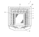
次に、本実施形態の有機EL装置1の具体的な態様を、図2、図3を参照して説明する。ここで、図2は有機EL装置の構成を模式的に示す平面図である。図3は有機EL装置の構造を模式的に示す断面図である。
Next, specific modes of the
まず、図2を参照し、有機EL装置1の構成を説明する。図2は、基板本体23上に形成された前述した各種配線,TFT,各種回路によって、発光層12を発光させるTFT素子基板(以下「素子基板」という。)23Aを示す図である。
有機EL装置1の素子基板23Aは、中央部分の実表示領域4(図2中二点鎖線枠内)と、実表示領域4の周囲に配置されたダミー領域5(一点鎖線および二点鎖線の間の領域)とを備えている。
First, the configuration of the
The
図1に示す画素領域Xからは、赤(R)、緑(G)または青(B)のいずれかの光が取り出され、図2に示す本発明の画素としてのサブ画素R,G,Bが構成されている。実表示領域4においては、サブ画素R,G,Bがマトリクス状に配置されている。また、サブ画素R,G,Bの各々は、紙面縦方向において同一色で配列しており、いわゆるストライプ配置を構成している。そして、サブ画素R,G,Bが一つのまとまりとなって、表示単位画素が構成されており、該表示単位画素はサブ画素R,G,Bの発光を混色させてフルカラー表示を行うようになっている。 One of red (R), green (G), and blue (B) light is extracted from the pixel region X shown in FIG. 1, and the sub-pixels R, G, B as the pixels of the present invention shown in FIG. Is configured. In the actual display area 4, the sub-pixels R, G, and B are arranged in a matrix. In addition, each of the sub-pixels R, G, and B is arranged in the same color in the vertical direction on the paper surface, and forms a so-called stripe arrangement. The sub-pixels R, G, and B are combined into one display unit pixel, and the display unit pixel performs full-color display by mixing the light emission of the sub-pixels R, G, and B. It has become.
実表示領域4を挟んだ左右両側であってダミー領域5の下層側には、それぞれ走査線駆動回路80が配置されている。また、実表示領域4の上方側であってダミー領域5の下層側には、検査回路90が配置されている。この検査回路90は、有機EL装置1の作動状況を検査するための回路であって、例えば検査結果を外部に出力する検査情報出力手段(不図示)を備え、製造途中や出荷時における有機EL装置1の品質、欠陥の検査を行うことができるように構成されている。
On the left and right sides of the actual display area 4 and on the lower layer side of the dummy area 5, scanning
(断面構造)
次に、図3を参照して、有機EL装置1の断面構造を説明する。
図3に示すように、有機EL装置1は、陽極10と陰極11(一対の電極)の間に発光層12(有機発光層)を挟持した複数の発光素子24及び発光素子24を区切る画素隔壁13を有する素子基板23Aと、この素子基板23Aに対向配置された封止基板31と、を有している。
本実施形態における有機EL装置1は、いわゆる「トップエミッション構造」の有機EL装置である。トップエミッション構造は、光を素子基板23A側ではなく封止基板31側から取り出すため、素子基板23Aに配置された各種回路の大きさに影響されず、発光面積を広く確保できる効果がある。そのため、電圧及び電流を抑えつつ輝度を確保することが可能であり、発光素子の寿命を長く維持することができる。
(Cross-section structure)
Next, a cross-sectional structure of the
As shown in FIG. 3, the
The
(素子基板)
図3に示すように、有機EL装置1は、前述した各種配線(例えば、TFT等)が形成された素子基板23A上に、窒化珪素等からなる無機絶縁層14が被覆されている。また、無機絶縁層14にはコンタクトホール(不図示)が形成され、前述した陽極10が駆動用TFT123に接続されている。無機絶縁層14上にはアルミ合金等からなる金属反射板15が内装された平坦化層16が形成されている。
この平坦化層16上には、陽極10と陰極11とが発光層12を挟持して形成され、発光素子24を構成している。また、この発光素子24を区分するように絶縁性の画素隔壁13が配置されている。
(Element board)
As shown in FIG. 3, in the
On the
本実施形態において、陽極10は、仕事関数が5eV以上の正孔注入層の高いITO(Indium Thin Oxide;インジウム錫酸化物)等の金属酸化物導電膜が用いられる。
なお、本実施形態においては、トップエミッション構造のため、陽極10は必ずしも光透過性を有する材料を用いる必要はなく、アルミ等からなる金属電極を用いてもよい。この構成を採用した場合は、前述した金属反射板15は設けなくてよい。
In the present embodiment, the
In the present embodiment, because of the top emission structure, the
陰極11を形成するための材料としては、本実施形態はトップエミッション構造であることから光透過性を有する材料である必要があり、透明導電材料が用いられる。透明導電材料としては、ITOが好適とされるが、これ以外にも、例えば酸化インジウム・酸化亜鉛系アモルファス透明導電膜(Indium Zinc Oxide:IZO/アイ・ゼット・オー(登録商標))等を用いることができる。なお、本実施形態ではITOを用いるものとする。
As a material for forming the
また、陰極11は、電子注入効果の大きい(仕事関数が4eV以下)材料が好適に用いられる。例えば、カルシウムやマグネシウム、ナトリウム、リチウム金属、又はこれらの金属化合物である。金属化合物としては、フッ化カルシウム等の金属フッ化物や酸化リチウム等の金属酸化物、アセチルアセトナトカルシウム等の有機金属錯体が該当する。また、これらの材料だけでは、電気抵抗が大きく電極として機能しないため、発光部分を避けるようにアルミニウムや金、銀、銅などの金属層をパターン形成したり、ITOや酸化錫などの透明な金属酸化物導電層を組み合わせた積層体としてもよい。なお、本実施形態では、フッ化リチウムとマグネシウム−銀合金、ITOの積層体を、透明性が得られる膜厚に調整して用いるものとする。
For the
発光層12は、白色に発光する白色発光層を採用している。この白色発光層は、真空蒸着プロセスを用いて素子基板23Aの全面に形成されている。白色発光材料としては、スチリルアミン系発光材料,アントラセン系ドーパミント(青色)、或いはスチリルアミン系発光材料,ルブレン系ドーパミント(黄色)が用いられる。
なお、発光層12の下層にトリアリールアミン(ATP)多量体正孔注入層やTDP(トリフェニルジアミン)系正孔輸送層を成膜し、発光層12の上層にアルミニウムキノリノール(Alq3)層(電子輸送層)を成膜することが好ましい。
The
A triarylamine (ATP) multimer hole injection layer or a TDP (triphenyldiamine) hole transport layer is formed below the
また、素子基板23A上には、発光素子24及び画素隔壁13を被覆するように封止膜17が形成されている。
この封止膜17は、透明性や密着性、耐水性、ガスバリア性を考慮して酸化珪素、窒化珪素、酸化窒化珪素などの珪素化合物で構成することが望ましい。また、封止膜17の膜厚は100nm以上が好ましく、画素隔壁13を被覆することで発生する応力によるクラック発生を防ぐため、膜厚の上限は400nm以下に設定することが好ましい。
なお、本実施形態においては、封止膜17を単層で形成しているが、複数層で積層してもよい。例えば、低弾性率の下層と高耐水性の上層とで封止膜17を構成してもよい。
また、封止膜は、珪素化合物に限らず酸化アルミニウムを用いて構成してもよい。
A sealing
The sealing
In the present embodiment, the sealing
Further, the sealing film is not limited to the silicon compound, and may be configured using aluminum oxide.
封止膜17上には、マイクロレンズ18が形成されている。
このマイクロレンズ18は、画素隔壁13の開口を覆うように配置され、凸状に形成される。このマイクロレンズ18の形成方法としては、フォトリソグラフィ法やインクジェット法などの塗布方式により、フッ素系樹脂や酸化チタンなどの無機ナノ粒子を混入したアクリル樹脂など屈折率が1.6以上の樹脂を塗布してサブ画素ごとにパターニングする方法が挙げられる。
マイクロレンズ18にこれらの樹脂をもちいる理由としては、屈折率が高くまた、弾性率が10GPa以下と非常に低弾性率化が可能なためである。この結果、素子基板23Aの反りや体積膨張により発生する応力を緩和し、不安定な形状の画素隔壁13からの封止膜17の剥離を防止する機能を有する。さらに、その上部に配置する平坦化層20との応力を緩和させるためにマイクロレンズ18の立ち上がり角度は、70°以下で作製する。
A
The
The reason why these resins are used for the
また、ハイバリア性を求める構造にする場合は、その上部に配置される平坦化層20に100GPa以上の弾性率を求めれるため、マイクロレンズ18の弾性率を1GPa以下まで(望ましくは0.1GPa)可能な限り低くするか、もしくは立ち上がり角度を20°以下まで(望ましくは5°)可能な限り低角度にする必要がある。
また、マイクロレンズ18の代わりに断面が円弧状のシリンドリカルレンズ19を同色のサブ画素に跨ってストライプ状に配置してもよい。
In the case of a structure that requires high barrier properties, the elastic modulus of the
Further, instead of the
平坦化層20は、マイクロレンズ18の形成の際に生じた凹凸部分を埋めるように配置され、さらに、その上面は略平坦に形成される。
このような平坦化層20の形成方法としては、スピンコート法やスリットコート法などの塗布方式が用いられ、この材料としては、SiO(酸化シリコン)を骨格とした無機膜あるいは有機膜と無機膜のハイブリッド膜を用いる。
SiO(酸化シリコン)を骨格とした無機膜あるいは有機膜と無機膜のハイブリッド膜は、通常、透過性が高くかつ屈折率が1.4前後であり、マイクロレンズ18との屈折率差によりマイクロレンズ18が光学レンズとして機能することができる。このときの屈折率差は、レンズとして機能させるため、大きければ大きいほどよい(0.3以上が好ましい)。そのため、マイクロレンズ18には、樹脂として可能な1.6以上、具体的には1.6〜1.9の高屈折率が必要となり、また平坦化層20には1.5以下、具体的には1.2〜1.5の低屈折率が必要となる。
The
As a method for forming such a
An inorganic film having an SiO (silicon oxide) skeleton or a hybrid film of an organic film and an inorganic film usually has high permeability and a refractive index of around 1.4, and the microlens is different from the refractive index difference with the
更に平坦化層20の上面に第2封止膜21が形成される。第2封止膜21の弾性率は、100GPa以上、具体的には200GPa〜250GPa程度が好ましい。また、第2封止膜21の膜厚は、200nm〜600nm程度が好ましい。200nm未満であると、異物に対する被覆性が不足し部分的に貫通孔が形成されてしまい、ガスバリア性が損なわれてしまうおそれがあるからであり、600nmを越えると、応力によるクラックが生じてしまうおそれがあるからである。
Further, a
また、本実施形態では、有機EL装置1をトップエミッション構造としていることから、第2封止膜21は光透過性を有する必要があり、したがってその材質や膜厚を適宜に調整することにより、本実施形態では可視光領域における光線透過率を例えば80%以上にしている。
Further, in the present embodiment, since the
第2封止膜21の上面には、カラーフィルター層22が形成される。カラーフィルター層22は、フォトリソグラフィ法やインクジェット法により形成され、RGBのカラーレジストを各サブ画素色に対応し、パターニングする。また、発光素子24を高温に晒すことは好ましくないので、例えば120℃以下にて減圧下での焼成や紫外線を当てることによって硬化する樹脂を使用する。
A
(封止基板)
さらに、カラーフィルター層22が形成された素子基板23Aに封止基板31が対向配置される。
この封止基板31は、発光光を取り出す表示面を構成するため、ガラスまたは透明プラスチック(ポリエチレンテレフタレート、アクリル樹脂、ポリカーボネ―ト、ポリオレフィン等)などの光透過性を有する材料が用いられている。
(Sealing substrate)
Further, the sealing
The sealing
また、素子基板23Aと封止基板31との間の周辺部に周辺シール層33が設けられている。
この周辺シール層33は、素子基板23Aと封止基板31の貼り合わせの位置精度の向上と後述する充填層34(接着剤層)のはみ出しを防止する土手の機能を有し、紫外線によって硬化して粘度が向上するエポキシ材料等で構成されている。好ましくは、エポキシ基を有する分子量3000以下のエポキシモノマー/オリゴマーが用いられる(モノマーの定義:分子量1000以下、オリゴマーの定義:分子量1000〜3000)。例えば、ビスフェノールA型エポキシオリゴマーやビスフェノールF型エポキシオリゴマー、フェノールノボラック型エポキシオリゴマー、ポリエチレングリコールジグリシジルエーテル、アルキルグリシジルエーテル、3,4-エポキシシクロヘキセニルメチル-3',4'-エポキシシクロヘキセンカルボキシレート、ε-カプロラクトン変性3,4-エポキシシクロヘキシルメチル3',4'-エポキシシクロヘキサンカルボキレートなどがあり、これらが単独もしくは複数組み合わされて用いられる。
In addition, a peripheral seal layer 33 is provided in the peripheral portion between the
The peripheral sealing layer 33 has a bank function for improving the positional accuracy of the bonding between the
また、エポキシモノマー/オリゴマーと反応する硬化剤としては、ジアゾニウム塩、ジフェニルヨウドニウム塩、トリフェルスルフォニウム塩、スルホン酸エステル、鉄アレーン錯体、シラノール/アルミニウム錯体などのカチオン重合反応を起こす光反応型開始剤が好ましい。また、紫外線照射後に徐々に粘度が上昇する材料を用いると、1mm以下の細いシール幅でも周辺シール層33の断裂を防ぎ、貼り合わせ後の充填剤のはみ出しを防ぐことができる。また、減圧しながら貼り合わせ時に気泡を発生し難くするため、含水量は1000ppm以下に調整された材料であることが好ましい。 In addition, as a curing agent that reacts with epoxy monomer / oligomer, photoreactive type that causes cationic polymerization reaction such as diazonium salt, diphenyliodonium salt, trifellsulfonium salt, sulfonate ester, iron arene complex, silanol / aluminum complex, etc. Initiators are preferred. In addition, when a material whose viscosity gradually increases after ultraviolet irradiation is used, the peripheral seal layer 33 can be prevented from tearing even with a narrow seal width of 1 mm or less, and the filler can be prevented from sticking out after bonding. Further, in order to make it difficult for bubbles to be generated at the time of bonding while reducing the pressure, it is preferable that the water content is a material adjusted to 1000 ppm or less.
周辺シール層33の膜厚としては、画素隔壁13、封止膜17、マイクロレンズ18、平坦化層20、および充填層34の総膜厚を考慮し、10μm〜25μmが好ましい。なお、素子基板23Aと封止基板31との距離を規制するために所定粒径の有機材料からなる球状粒子が混合されているものが好ましい。通常、無機材料の燐片状や塊状の粒子を混合してシール剤の粘度を高めているが、前述した第2封止膜21が貼り合わせ圧着時に損傷してしまうため、本実施形態における有機EL装置1は、弾性率が小さい有機材料の球状粒子を周辺シール層33に混合している。なお、周辺シール層33は、封止膜17、平坦化層20および第2封止膜21の端部上に設けられるように配置したが、これに限定されない。封止膜17、平坦化層20および第2封止膜21の端部よりも素子基板23Aの外周側に周辺シール層33を配置してもよい。
The film thickness of the peripheral sealing layer 33 is preferably 10 μm to 25 μm in consideration of the total film thickness of the
また、素子基板23Aと封止基板31の間における周辺シール層33に囲まれた内部に、熱硬化性樹脂からなる充填層34(接着剤層)が形成されている。
この充填層34は、前述した周辺シール層33で囲まれた有機EL装置1の内部に隙間なく充填されており、素子基板23Aに対向配置された封止基板31を固定させ、かつ外部からの機械的衝撃に対して緩衝機能を有し、発光層12や第2封止膜21の保護をするものである。
A filling layer 34 (adhesive layer) made of a thermosetting resin is formed inside the
The filling
充填層34は、硬化前の原料主成分としては、流動性に優れ、かつ溶媒のような揮発成分を持たない有機化合物材料である必要があり、好ましくはエポキシ基を有する分子量3000以下のエポキシモノマー/オリゴマーが用いられる(モノマーの定義:分子量1000以下、オリゴマーの定義:分子量1000〜3000)。例えば、ビスフェノールA型エポキシオリゴマーやビスフェノールF型エポキシオリゴマー、フェノールノボラック型エポキシオリゴマー、ポリエチレングリコールジグリシジルエーテル、アルキルグリシジルエーテル、3,4-エポキシシクロヘキセニルメチル-3',4'-エポキシシクロヘキセンカルボキシレート、ε-カプロラクトン変性3,4-エポキシシクロヘキシルメチル3',4'-エポキシシクロヘキサンカルボキレートなどがあり、これらが単独もしくは複数組み合わされて用いられる。
The packed
また、エポキシモノマー/オリゴマーと反応する硬化剤としては、電気絶縁性に優れ、かつ強靭で耐熱性に優れる硬化皮膜を形成するものが良く、透明性に優れ、かつ硬化のばらつきの少ない付加重合型が良い。例えば、3−メチル−1,2,3,6−テトラヒドロ無水フタル酸、メチル−3,6−エンドメチレン−1,2,3,6−テトラヒドロ無水フタル酸、1,2,4,5−ベンゼンテトラカルボン酸二無水物、3,3’,4,4’−ベンゾフェノンテトラカルボン酸二無水物、またはそれらの重合物などの酸無水物系硬化剤が好ましい。これらの硬化は、60℃〜100℃の範囲で行われ、その硬化皮膜は珪素酸窒化物との密着性に優れるエステル結合を持つ高分子となる。さらに、酸無水の開環を促進する硬化促進剤として芳香族アミンやアルコール類、アミノフェノール等の比較的分子量の高いものを添加することで低温かつ短時間での硬化が可能となる。 Further, as the curing agent that reacts with the epoxy monomer / oligomer, an addition polymerization type that is excellent in electrical insulation, forms a cured film that is tough and excellent in heat resistance, has excellent transparency, and has little variation in curing. Is good. For example, 3-methyl-1,2,3,6-tetrahydrophthalic anhydride, methyl-3,6-endomethylene-1,2,3,6-tetrahydrophthalic anhydride, 1,2,4,5-benzene An acid anhydride curing agent such as tetracarboxylic dianhydride, 3,3 ′, 4,4′-benzophenone tetracarboxylic dianhydride, or a polymer thereof is preferable. These curings are performed in a range of 60 ° C. to 100 ° C., and the cured film becomes a polymer having an ester bond that is excellent in adhesion to silicon oxynitride. Furthermore, curing at a low temperature and in a short time is possible by adding a relatively high molecular weight material such as an aromatic amine, alcohol, aminophenol or the like as a curing accelerator that promotes ring opening of acid anhydride.
また、塗布時の粘度は、100mPa・s〜1000mPa・s(室温)が好ましい。理由は、貼り合わせ後の空間への材料充填性を考慮したもので、加熱直後に一度粘度が下がってから硬化が始まる材料が好ましい。また、貼り合わせ時に減圧した際に気泡が発生しにくくするため、含水量は100ppm以下に調整された材料であることが好ましい。 The viscosity at the time of application is preferably 100 mPa · s to 1000 mPa · s (room temperature). The reason is that the material filling property into the space after the bonding is taken into consideration, and a material in which the curing starts after the viscosity once decreases immediately after heating is preferable. Further, in order to make it difficult for bubbles to be generated when the pressure is reduced at the time of bonding, it is preferable that the water content is a material adjusted to 100 ppm or less.
充填層34の膜厚としては、5μm〜20μmが好ましい。なお、素子基板23Aと封止基板31との距離を規制するために所定粒径の有機材料からなる球状粒子が混合されているものが好ましい。また、前述した周辺シール層33と同様に、本実施形態における有機EL装置1は、上記有機材料からなる球状粒子と同じ、弾性率が小さい有機材料の粒子を混合している。粒子に弾性率が小さい有機材料を充填層34に混合することにより、前述した第2封止膜21の損傷を防ぐことができる。
The film thickness of the
(電子機器)
次に、上記実施形態の有機EL装置を備えた電子機器の例について図4(a)〜(c)を参照して説明する。
図4(a)は、携帯電話の一例を示した斜視図である。図4(a)において、符号50は携帯電話本体を示し、符号51は有機EL装置1を備えた表示部を示している。
図4(b)は、ワープロ、パソコンなどの携帯型情報処理装置の一例を示した斜視図である。図4(b)において、符号60は情報処理装置、符号61はキーボードなどの入力部、符号63は情報処理本体、符号62は有機EL装置1を備えた表示部を示している。
図4(c)は、腕時計型電子機器の一例を示した斜視図である。図4(c)において、符号70は時計本体を示し、符号71は有機EL装置1を備えたEL表示部を示している。
図4(a)〜(c)に示す電子機器は、先の実施形態に示した有機EL装置1が備えられたものであるので、表示特性が良好な電子機器となる。
(Electronics)
Next, an example of an electronic apparatus provided with the organic EL device of the above embodiment will be described with reference to FIGS.
FIG. 4A is a perspective view showing an example of a mobile phone. In FIG. 4A,
FIG. 4B is a perspective view showing an example of a portable information processing apparatus such as a word processor or a personal computer. 4B,
FIG. 4C is a perspective view showing an example of a wristwatch type electronic device. In FIG. 4C, reference numeral 70 denotes a watch body, and reference numeral 71 denotes an EL display unit including the
Since the electronic devices shown in FIGS. 4A to 4C are provided with the
なお、電子機器としては、上記電子機器に限られることなく、種々の電子機器に適用することができる。例えば、ディスクトップ型コンピューター、液晶プロジェクター、マルチメディア対応のパーソナルコンピューター(PC)及びエンジニアリング・ワークステーション(EWS)、ページャー、ワードプロセッサー、テレビ、ビューファインダー型又はモニター直視型のビデオテープレコーダー、電子手帳、電子卓上計算機、カーナビゲーション装置、POS端末、タッチパネルを備えた装置等の電子機器に適用することができる。 In addition, as an electronic device, it is not restricted to the said electronic device, It can apply to a various electronic device. For example, desktop computers, liquid crystal projectors, multimedia personal computers (PCs) and engineering workstations (EWS), pagers, word processors, TVs, viewfinder type or monitor direct view type video tape recorders, electronic notebooks, electronic The present invention can be applied to electronic devices such as a desktop computer, a car navigation device, a POS terminal, and a device having a touch panel.
1…有機EL装置、10…陽極(一対の電極)、11…陰極(一対の電極)、12…発光層(有機発光層)、13…画素隔壁、17…封止膜、18…マイクロレンズ、19…シリンドリカルレンズ、20…平坦化層、21…第2封止膜、22…カラーフィルター層、23A…基板としての素子基板、31…封止基板、33…周辺シール層、34…充填層(接着剤層)。
DESCRIPTION OF
Claims (11)
前記基板上に形成された有機発光層を含む複数の画素と、
前記複数の画素を覆う封止膜と、
前記封止膜を介して前記画素を覆うマイクロレンズと、
複数の前記マイクロレンズを覆う平坦化層と、
前記平坦化層上において前記画素ごとに形成されたカラーフィルターと、を備え、
前記マイクロレンズの屈折率が、前記平坦化層の屈折率よりも大きいことを特徴とする発光装置。 A plurality of pixels including a substrate and an organic light emitting layer formed on the substrate;
A sealing film covering the plurality of pixels;
A microlens that covers the pixel through the sealing film;
A planarization layer covering a plurality of the microlenses;
A color filter formed for each of the pixels on the planarizing layer,
A light-emitting device, wherein a refractive index of the microlens is larger than a refractive index of the planarization layer.
前記平坦化層の屈折率が1.2以上1.5以下で形成されていることを特徴とする請求項1に記載の発光装置。 The refractive index of the microlens satisfies 1.6 or more and 1.9 or less,
The light emitting device according to claim 1, wherein the planarization layer has a refractive index of 1.2 to 1.5.
Priority Applications (1)
| Application Number | Priority Date | Filing Date | Title |
|---|---|---|---|
| JP2011081639A JP2012216454A (en) | 2011-04-01 | 2011-04-01 | Light-emitting device and electronic apparatus |
Applications Claiming Priority (1)
| Application Number | Priority Date | Filing Date | Title |
|---|---|---|---|
| JP2011081639A JP2012216454A (en) | 2011-04-01 | 2011-04-01 | Light-emitting device and electronic apparatus |
Publications (2)
| Publication Number | Publication Date |
|---|---|
| JP2012216454A true JP2012216454A (en) | 2012-11-08 |
| JP2012216454A5 JP2012216454A5 (en) | 2014-05-15 |
Family
ID=47269056
Family Applications (1)
| Application Number | Title | Priority Date | Filing Date |
|---|---|---|---|
| JP2011081639A Withdrawn JP2012216454A (en) | 2011-04-01 | 2011-04-01 | Light-emitting device and electronic apparatus |
Country Status (1)
| Country | Link |
|---|---|
| JP (1) | JP2012216454A (en) |
Cited By (12)
| Publication number | Priority date | Publication date | Assignee | Title |
|---|---|---|---|---|
| KR20160029087A (en) * | 2013-07-08 | 2016-03-14 | 픽셀리전트 테크놀로지스 엘엘씨 | Advanced light extraction structure |
| US9666646B2 (en) | 2013-10-10 | 2017-05-30 | Seiko Epson Corporation | Light emitting element disposed in a display region of a substrate |
| CN107026239A (en) * | 2016-09-22 | 2017-08-08 | 广东聚华印刷显示技术有限公司 | Organic electroluminescence device and its preparation method and application |
| US9786866B2 (en) | 2014-10-08 | 2017-10-10 | Japan Display Inc. | Display device with auxiliary wiring |
| CN110828517A (en) * | 2019-11-08 | 2020-02-21 | 京东方科技集团股份有限公司 | Display substrate, manufacturing method thereof and display device |
| CN111276515A (en) * | 2020-02-07 | 2020-06-12 | 武汉华星光电半导体显示技术有限公司 | OLED display panel and preparation method thereof |
| CN111816789A (en) * | 2020-07-24 | 2020-10-23 | 京东方科技集团股份有限公司 | Display substrate and manufacturing method thereof |
| CN112349872A (en) * | 2020-11-05 | 2021-02-09 | 合肥京东方卓印科技有限公司 | Display screen packaging method, display screen and electronic equipment |
| WO2021069999A1 (en) * | 2019-10-11 | 2021-04-15 | 株式会社半導体エネルギー研究所 | Function panel, display device, i/o device, and information processing device |
| CN112736109A (en) * | 2019-10-14 | 2021-04-30 | 成都辰显光电有限公司 | Display panel and method for manufacturing display panel |
| CN113054135A (en) * | 2021-03-09 | 2021-06-29 | 武汉华星光电半导体显示技术有限公司 | Display panel and display device |
| WO2023236676A1 (en) * | 2022-06-10 | 2023-12-14 | 京东方科技集团股份有限公司 | Display substrate and manufacturing method therefor, and display device |
Citations (8)
| Publication number | Priority date | Publication date | Assignee | Title |
|---|---|---|---|---|
| JP2004127661A (en) * | 2002-10-01 | 2004-04-22 | Sony Corp | Manufacturing method of display device |
| JP2004235261A (en) * | 2003-01-28 | 2004-08-19 | Matsushita Electric Works Ltd | Optical system device and its manufacturing method |
| JP2007207656A (en) * | 2006-02-03 | 2007-08-16 | Dainippon Printing Co Ltd | Organic el-display |
| JP2007216573A (en) * | 2006-02-17 | 2007-08-30 | Hitachi Maxell Ltd | Manufacturing method of optical lens sheet and optical lens sheet |
| JP2009048834A (en) * | 2007-08-17 | 2009-03-05 | Seiko Epson Corp | Organic electroluminescent device, manufacturing method thereof, and electronic equipment |
| JP2009186657A (en) * | 2008-02-05 | 2009-08-20 | Dainippon Printing Co Ltd | Dyestuff-pigment composite color filter and organic el display |
| JP2010040427A (en) * | 2008-08-07 | 2010-02-18 | Hitachi Displays Ltd | Organic electroluminescent display device |
| WO2010087238A1 (en) * | 2009-01-29 | 2010-08-05 | 東レ株式会社 | Resin composition and display device formed using same |
-
2011
- 2011-04-01 JP JP2011081639A patent/JP2012216454A/en not_active Withdrawn
Patent Citations (8)
| Publication number | Priority date | Publication date | Assignee | Title |
|---|---|---|---|---|
| JP2004127661A (en) * | 2002-10-01 | 2004-04-22 | Sony Corp | Manufacturing method of display device |
| JP2004235261A (en) * | 2003-01-28 | 2004-08-19 | Matsushita Electric Works Ltd | Optical system device and its manufacturing method |
| JP2007207656A (en) * | 2006-02-03 | 2007-08-16 | Dainippon Printing Co Ltd | Organic el-display |
| JP2007216573A (en) * | 2006-02-17 | 2007-08-30 | Hitachi Maxell Ltd | Manufacturing method of optical lens sheet and optical lens sheet |
| JP2009048834A (en) * | 2007-08-17 | 2009-03-05 | Seiko Epson Corp | Organic electroluminescent device, manufacturing method thereof, and electronic equipment |
| JP2009186657A (en) * | 2008-02-05 | 2009-08-20 | Dainippon Printing Co Ltd | Dyestuff-pigment composite color filter and organic el display |
| JP2010040427A (en) * | 2008-08-07 | 2010-02-18 | Hitachi Displays Ltd | Organic electroluminescent display device |
| WO2010087238A1 (en) * | 2009-01-29 | 2010-08-05 | 東レ株式会社 | Resin composition and display device formed using same |
Cited By (22)
| Publication number | Priority date | Publication date | Assignee | Title |
|---|---|---|---|---|
| KR102294665B1 (en) * | 2013-07-08 | 2021-08-31 | 픽셀리전트 테크놀로지스 엘엘씨 | Advanced light extraction structure |
| KR102624558B1 (en) | 2013-07-08 | 2024-01-15 | 피티 에스피이 서브코 엘엘씨 | Advanced light extraction structure |
| KR20220104312A (en) * | 2013-07-08 | 2022-07-26 | 픽셀리전트 테크놀로지스 엘엘씨 | Advanced light extraction structure |
| KR102424685B1 (en) | 2013-07-08 | 2022-07-25 | 픽셀리전트 테크놀로지스 엘엘씨 | Advanced light extraction structure |
| KR20160029087A (en) * | 2013-07-08 | 2016-03-14 | 픽셀리전트 테크놀로지스 엘엘씨 | Advanced light extraction structure |
| KR20210107898A (en) * | 2013-07-08 | 2021-09-01 | 픽셀리전트 테크놀로지스 엘엘씨 | Advanced light extraction structure |
| US9666646B2 (en) | 2013-10-10 | 2017-05-30 | Seiko Epson Corporation | Light emitting element disposed in a display region of a substrate |
| US10177336B2 (en) | 2014-10-08 | 2019-01-08 | Japan Display Inc. | Method of manufacturing a display device with an auxiliary wiring |
| KR101862443B1 (en) * | 2014-10-08 | 2018-07-04 | 가부시키가이샤 재팬 디스프레이 | Display device and method of manufacturing the same |
| US9786866B2 (en) | 2014-10-08 | 2017-10-10 | Japan Display Inc. | Display device with auxiliary wiring |
| CN107026239A (en) * | 2016-09-22 | 2017-08-08 | 广东聚华印刷显示技术有限公司 | Organic electroluminescence device and its preparation method and application |
| WO2021069999A1 (en) * | 2019-10-11 | 2021-04-15 | 株式会社半導体エネルギー研究所 | Function panel, display device, i/o device, and information processing device |
| US20220338316A1 (en) * | 2019-10-11 | 2022-10-20 | Semiconductor Energy Laboratory Co., Ltd. | Functional Panel, Display Device, Input/Output Device, and Data Processing Device |
| CN112736109A (en) * | 2019-10-14 | 2021-04-30 | 成都辰显光电有限公司 | Display panel and method for manufacturing display panel |
| CN112736109B (en) * | 2019-10-14 | 2022-12-20 | 成都辰显光电有限公司 | Display panel and method for manufacturing display panel |
| CN110828517A (en) * | 2019-11-08 | 2020-02-21 | 京东方科技集团股份有限公司 | Display substrate, manufacturing method thereof and display device |
| CN111276515A (en) * | 2020-02-07 | 2020-06-12 | 武汉华星光电半导体显示技术有限公司 | OLED display panel and preparation method thereof |
| CN111816789A (en) * | 2020-07-24 | 2020-10-23 | 京东方科技集团股份有限公司 | Display substrate and manufacturing method thereof |
| US11765930B2 (en) | 2020-07-24 | 2023-09-19 | Boe Technology Group Co., Ltd. | Display substrate and method for manufacturing the same |
| CN112349872A (en) * | 2020-11-05 | 2021-02-09 | 合肥京东方卓印科技有限公司 | Display screen packaging method, display screen and electronic equipment |
| CN113054135A (en) * | 2021-03-09 | 2021-06-29 | 武汉华星光电半导体显示技术有限公司 | Display panel and display device |
| WO2023236676A1 (en) * | 2022-06-10 | 2023-12-14 | 京东方科技集团股份有限公司 | Display substrate and manufacturing method therefor, and display device |
Similar Documents
| Publication | Publication Date | Title |
|---|---|---|
| JP2012216454A (en) | Light-emitting device and electronic apparatus | |
| JP4337852B2 (en) | ORGANIC ELECTROLUMINESCENT DEVICE, ITS MANUFACTURING METHOD, AND ELECTRONIC DEVICE | |
| JP4670875B2 (en) | Organic EL device | |
| US7915823B2 (en) | Organic electroluminescent device with surface-modifying layer, method for manufacturing the same, and electronic apparatus including the same | |
| JP5119865B2 (en) | Organic electroluminescence equipment, electronic equipment | |
| JP5741274B2 (en) | Organic EL device and electronic device | |
| JP2008059868A (en) | Organic electroluminescent device, its manufacturing method, and electronic apparatus | |
| JP2008066216A (en) | Organic electroluminescence device, its manufacturing method and electronic apparatus | |
| JP2011228229A (en) | Organic electroluminescent device | |
| JP2014035799A (en) | Light-emitting device, manufacturing method therefor, electronic apparatus | |
| JP5056777B2 (en) | ORGANIC ELECTROLUMINESCENCE DEVICE, ITS MANUFACTURING METHOD, AND ELECTRONIC DEVICE | |
| JP2017147051A (en) | Electro-optical device and electronic equipment | |
| JP2012209215A (en) | Manufacturing method of organic el device and electronic apparatus | |
| JP2009048834A (en) | Organic electroluminescent device, manufacturing method thereof, and electronic equipment | |
| JP2010033734A (en) | Organic electroluminescent device | |
| JP2012209116A (en) | Manufacturing method of organic electroluminescent device and electronic apparatus | |
| JP2009048835A (en) | Organic electroluminescent device and manufacturing method thereof, as well as electronic equipment | |
| JP5228513B2 (en) | Organic EL device | |
| JP2008089634A (en) | Electro-optical device and electronic equipment | |
| JP5012848B2 (en) | Organic electroluminescence device and electronic device | |
| JP2010231908A (en) | Organic electroluminescent device, electronic equipment | |
| JP2009252687A (en) | Method for manufacturing of organic electroluminescent device, and the organic electroluminescent device | |
| JP2011018508A (en) | Electrooptic device and electronic equipment | |
| JP5741046B2 (en) | Electro-optical device, method of manufacturing electro-optical device, and electronic apparatus | |
| JP2008123879A (en) | Method of manufacturing organic el device, and organic el device |
Legal Events
| Date | Code | Title | Description |
|---|---|---|---|
| A521 | Request for written amendment filed |
Free format text: JAPANESE INTERMEDIATE CODE: A523 Effective date: 20140328 |
|
| A621 | Written request for application examination |
Free format text: JAPANESE INTERMEDIATE CODE: A621 Effective date: 20140328 |
|
| RD04 | Notification of resignation of power of attorney |
Free format text: JAPANESE INTERMEDIATE CODE: A7424 Effective date: 20150106 |
|
| A977 | Report on retrieval |
Free format text: JAPANESE INTERMEDIATE CODE: A971007 Effective date: 20150126 |
|
| A131 | Notification of reasons for refusal |
Free format text: JAPANESE INTERMEDIATE CODE: A131 Effective date: 20150203 |
|
| A761 | Written withdrawal of application |
Free format text: JAPANESE INTERMEDIATE CODE: A761 Effective date: 20150324 |