JP5012848B2 - Organic electroluminescence device and electronic device - Google Patents
Organic electroluminescence device and electronic device Download PDFInfo
- Publication number
- JP5012848B2 JP5012848B2 JP2009116273A JP2009116273A JP5012848B2 JP 5012848 B2 JP5012848 B2 JP 5012848B2 JP 2009116273 A JP2009116273 A JP 2009116273A JP 2009116273 A JP2009116273 A JP 2009116273A JP 5012848 B2 JP5012848 B2 JP 5012848B2
- Authority
- JP
- Japan
- Prior art keywords
- layer
- organic
- substrate
- peripheral
- light emitting
- Prior art date
- Legal status (The legal status is an assumption and is not a legal conclusion. Google has not performed a legal analysis and makes no representation as to the accuracy of the status listed.)
- Expired - Fee Related
Links
- 238000005401 electroluminescence Methods 0.000 title claims description 14
- 239000010410 layer Substances 0.000 claims description 355
- 239000000758 substrate Substances 0.000 claims description 173
- 230000002093 peripheral effect Effects 0.000 claims description 128
- 238000007789 sealing Methods 0.000 claims description 119
- 239000002245 particle Substances 0.000 claims description 14
- 229920005989 resin Polymers 0.000 claims description 13
- 239000011347 resin Substances 0.000 claims description 13
- 239000012790 adhesive layer Substances 0.000 claims description 11
- 239000011368 organic material Substances 0.000 claims description 11
- 229920001187 thermosetting polymer Polymers 0.000 claims description 9
- 150000003377 silicon compounds Chemical class 0.000 claims description 7
- 239000012798 spherical particle Substances 0.000 claims description 7
- 239000011810 insulating material Substances 0.000 claims 1
- 230000004888 barrier function Effects 0.000 description 77
- 239000007789 gas Substances 0.000 description 77
- 239000000463 material Substances 0.000 description 46
- 238000001723 curing Methods 0.000 description 25
- 239000010408 film Substances 0.000 description 25
- 238000000034 method Methods 0.000 description 21
- -1 lithium oxide Chemical compound 0.000 description 19
- 238000011049 filling Methods 0.000 description 17
- 239000011241 protective layer Substances 0.000 description 17
- 239000004593 Epoxy Substances 0.000 description 16
- 239000011159 matrix material Substances 0.000 description 14
- 238000005192 partition Methods 0.000 description 13
- XLYOFNOQVPJJNP-UHFFFAOYSA-N water Substances O XLYOFNOQVPJJNP-UHFFFAOYSA-N 0.000 description 10
- 239000012298 atmosphere Substances 0.000 description 9
- 238000002347 injection Methods 0.000 description 9
- 239000007924 injection Substances 0.000 description 9
- 238000004519 manufacturing process Methods 0.000 description 9
- 239000000178 monomer Substances 0.000 description 9
- 239000003795 chemical substances by application Substances 0.000 description 8
- 230000000630 rising effect Effects 0.000 description 8
- 238000010586 diagram Methods 0.000 description 7
- 238000010438 heat treatment Methods 0.000 description 7
- IISBACLAFKSPIT-UHFFFAOYSA-N bisphenol A Chemical compound C=1C=C(O)C=CC=1C(C)(C)C1=CC=C(O)C=C1 IISBACLAFKSPIT-UHFFFAOYSA-N 0.000 description 6
- PXKLMJQFEQBVLD-UHFFFAOYSA-N bisphenol F Chemical compound C1=CC(O)=CC=C1CC1=CC=C(O)C=C1 PXKLMJQFEQBVLD-UHFFFAOYSA-N 0.000 description 6
- 230000007423 decrease Effects 0.000 description 6
- 230000000694 effects Effects 0.000 description 6
- 229910052581 Si3N4 Inorganic materials 0.000 description 5
- QVGXLLKOCUKJST-UHFFFAOYSA-N atomic oxygen Chemical compound [O] QVGXLLKOCUKJST-UHFFFAOYSA-N 0.000 description 5
- 229910052751 metal Inorganic materials 0.000 description 5
- 239000002184 metal Substances 0.000 description 5
- 239000001301 oxygen Substances 0.000 description 5
- 229910052760 oxygen Inorganic materials 0.000 description 5
- 239000002994 raw material Substances 0.000 description 5
- HQVNEWCFYHHQES-UHFFFAOYSA-N silicon nitride Chemical compound N12[Si]34N5[Si]62N3[Si]51N64 HQVNEWCFYHHQES-UHFFFAOYSA-N 0.000 description 5
- IJGRMHOSHXDMSA-UHFFFAOYSA-N Atomic nitrogen Chemical compound N#N IJGRMHOSHXDMSA-UHFFFAOYSA-N 0.000 description 4
- XUIMIQQOPSSXEZ-UHFFFAOYSA-N Silicon Chemical compound [Si] XUIMIQQOPSSXEZ-UHFFFAOYSA-N 0.000 description 4
- 239000003990 capacitor Substances 0.000 description 4
- 238000006243 chemical reaction Methods 0.000 description 4
- VYFYYTLLBUKUHU-UHFFFAOYSA-N dopamine Chemical compound NCCC1=CC=C(O)C(O)=C1 VYFYYTLLBUKUHU-UHFFFAOYSA-N 0.000 description 4
- 229910010272 inorganic material Inorganic materials 0.000 description 4
- 239000011147 inorganic material Substances 0.000 description 4
- 238000007689 inspection Methods 0.000 description 4
- PQXKHYXIUOZZFA-UHFFFAOYSA-M lithium fluoride Chemical compound [Li+].[F-] PQXKHYXIUOZZFA-UHFFFAOYSA-M 0.000 description 4
- 229920000642 polymer Polymers 0.000 description 4
- 229910052710 silicon Inorganic materials 0.000 description 4
- 239000010703 silicon Substances 0.000 description 4
- AOBIOSPNXBMOAT-UHFFFAOYSA-N 2-[2-(oxiran-2-ylmethoxy)ethoxymethyl]oxirane Chemical compound C1OC1COCCOCC1CO1 AOBIOSPNXBMOAT-UHFFFAOYSA-N 0.000 description 3
- ISWSIDIOOBJBQZ-UHFFFAOYSA-N Phenol Chemical compound OC1=CC=CC=C1 ISWSIDIOOBJBQZ-UHFFFAOYSA-N 0.000 description 3
- 239000002202 Polyethylene glycol Substances 0.000 description 3
- 229920000265 Polyparaphenylene Polymers 0.000 description 3
- VYPSYNLAJGMNEJ-UHFFFAOYSA-N Silicium dioxide Chemical compound O=[Si]=O VYPSYNLAJGMNEJ-UHFFFAOYSA-N 0.000 description 3
- 150000008065 acid anhydrides Chemical class 0.000 description 3
- 229910052782 aluminium Inorganic materials 0.000 description 3
- XAGFODPZIPBFFR-UHFFFAOYSA-N aluminium Chemical compound [Al] XAGFODPZIPBFFR-UHFFFAOYSA-N 0.000 description 3
- 230000003139 buffering effect Effects 0.000 description 3
- 239000011248 coating agent Substances 0.000 description 3
- 238000000576 coating method Methods 0.000 description 3
- 125000003700 epoxy group Chemical group 0.000 description 3
- 230000010365 information processing Effects 0.000 description 3
- 238000007733 ion plating Methods 0.000 description 3
- 230000001678 irradiating effect Effects 0.000 description 3
- 239000002346 layers by function Substances 0.000 description 3
- 239000000203 mixture Substances 0.000 description 3
- 229920003986 novolac Polymers 0.000 description 3
- 125000002080 perylenyl group Chemical group C1(=CC=C2C=CC=C3C4=CC=CC5=CC=CC(C1=C23)=C45)* 0.000 description 3
- CSHWQDPOILHKBI-UHFFFAOYSA-N peryrene Natural products C1=CC(C2=CC=CC=3C2=C2C=CC=3)=C3C2=CC=CC3=C1 CSHWQDPOILHKBI-UHFFFAOYSA-N 0.000 description 3
- 229920001223 polyethylene glycol Polymers 0.000 description 3
- 239000002861 polymer material Substances 0.000 description 3
- YYMBJDOZVAITBP-UHFFFAOYSA-N rubrene Chemical compound C1=CC=CC=C1C(C1=C(C=2C=CC=CC=2)C2=CC=CC=C2C(C=2C=CC=CC=2)=C11)=C(C=CC=C2)C2=C1C1=CC=CC=C1 YYMBJDOZVAITBP-UHFFFAOYSA-N 0.000 description 3
- 230000035939 shock Effects 0.000 description 3
- 239000010409 thin film Substances 0.000 description 3
- UWRZIZXBOLBCON-VOTSOKGWSA-N (e)-2-phenylethenamine Chemical compound N\C=C\C1=CC=CC=C1 UWRZIZXBOLBCON-VOTSOKGWSA-N 0.000 description 2
- CDAWCLOXVUBKRW-UHFFFAOYSA-N 2-aminophenol Chemical class NC1=CC=CC=C1O CDAWCLOXVUBKRW-UHFFFAOYSA-N 0.000 description 2
- XPEKVUUBSDFMDR-UHFFFAOYSA-N 4-methyl-3a,4,7,7a-tetrahydro-2-benzofuran-1,3-dione Chemical compound CC1C=CCC2C(=O)OC(=O)C12 XPEKVUUBSDFMDR-UHFFFAOYSA-N 0.000 description 2
- VQVIHDPBMFABCQ-UHFFFAOYSA-N 5-(1,3-dioxo-2-benzofuran-5-carbonyl)-2-benzofuran-1,3-dione Chemical compound C1=C2C(=O)OC(=O)C2=CC(C(C=2C=C3C(=O)OC(=O)C3=CC=2)=O)=C1 VQVIHDPBMFABCQ-UHFFFAOYSA-N 0.000 description 2
- OYPRJOBELJOOCE-UHFFFAOYSA-N Calcium Chemical compound [Ca] OYPRJOBELJOOCE-UHFFFAOYSA-N 0.000 description 2
- 229920000285 Polydioctylfluorene Polymers 0.000 description 2
- XLOMVQKBTHCTTD-UHFFFAOYSA-N Zinc monoxide Chemical compound [Zn]=O XLOMVQKBTHCTTD-UHFFFAOYSA-N 0.000 description 2
- GTDPSWPPOUPBNX-UHFFFAOYSA-N ac1mqpva Chemical compound CC12C(=O)OC(=O)C1(C)C1(C)C2(C)C(=O)OC1=O GTDPSWPPOUPBNX-UHFFFAOYSA-N 0.000 description 2
- 238000012644 addition polymerization Methods 0.000 description 2
- MWPLVEDNUUSJAV-UHFFFAOYSA-N anthracene Chemical compound C1=CC=CC2=CC3=CC=CC=C3C=C21 MWPLVEDNUUSJAV-UHFFFAOYSA-N 0.000 description 2
- UHOVQNZJYSORNB-UHFFFAOYSA-N benzene Substances C1=CC=CC=C1 UHOVQNZJYSORNB-UHFFFAOYSA-N 0.000 description 2
- 229910052791 calcium Inorganic materials 0.000 description 2
- 239000011575 calcium Substances 0.000 description 2
- 238000004040 coloring Methods 0.000 description 2
- 239000004020 conductor Substances 0.000 description 2
- ZYGHJZDHTFUPRJ-UHFFFAOYSA-N coumarin Chemical compound C1=CC=C2OC(=O)C=CC2=C1 ZYGHJZDHTFUPRJ-UHFFFAOYSA-N 0.000 description 2
- 230000007547 defect Effects 0.000 description 2
- 229960003638 dopamine Drugs 0.000 description 2
- 239000000975 dye Substances 0.000 description 2
- 238000010292 electrical insulation Methods 0.000 description 2
- 239000003999 initiator Substances 0.000 description 2
- 150000002736 metal compounds Chemical class 0.000 description 2
- 229910044991 metal oxide Inorganic materials 0.000 description 2
- 150000004706 metal oxides Chemical class 0.000 description 2
- 238000002156 mixing Methods 0.000 description 2
- VOFUROIFQGPCGE-UHFFFAOYSA-N nile red Chemical compound C1=CC=C2C3=NC4=CC=C(N(CC)CC)C=C4OC3=CC(=O)C2=C1 VOFUROIFQGPCGE-UHFFFAOYSA-N 0.000 description 2
- 229910052757 nitrogen Inorganic materials 0.000 description 2
- 150000002894 organic compounds Chemical class 0.000 description 2
- 229920003227 poly(N-vinyl carbazole) Polymers 0.000 description 2
- 230000002265 prevention Effects 0.000 description 2
- 238000007639 printing Methods 0.000 description 2
- 230000001105 regulatory effect Effects 0.000 description 2
- 238000007142 ring opening reaction Methods 0.000 description 2
- 238000007650 screen-printing Methods 0.000 description 2
- 239000012812 sealant material Substances 0.000 description 2
- 239000002904 solvent Substances 0.000 description 2
- 238000004544 sputter deposition Methods 0.000 description 2
- 125000006158 tetracarboxylic acid group Chemical group 0.000 description 2
- 238000002834 transmittance Methods 0.000 description 2
- TVIVIEFSHFOWTE-UHFFFAOYSA-K tri(quinolin-8-yloxy)alumane Chemical compound [Al+3].C1=CN=C2C([O-])=CC=CC2=C1.C1=CN=C2C([O-])=CC=CC2=C1.C1=CN=C2C([O-])=CC=CC2=C1 TVIVIEFSHFOWTE-UHFFFAOYSA-K 0.000 description 2
- 238000001771 vacuum deposition Methods 0.000 description 2
- FNQJDLTXOVEEFB-UHFFFAOYSA-N 1,2,3-benzothiadiazole Chemical compound C1=CC=C2SN=NC2=C1 FNQJDLTXOVEEFB-UHFFFAOYSA-N 0.000 description 1
- PZWLRLIAVLSBQU-UHFFFAOYSA-N 1,2-dioctyl-9h-fluorene Chemical compound C1=CC=C2C3=CC=C(CCCCCCCC)C(CCCCCCCC)=C3CC2=C1 PZWLRLIAVLSBQU-UHFFFAOYSA-N 0.000 description 1
- KLCLIOISYBHYDZ-UHFFFAOYSA-N 1,4,4-triphenylbuta-1,3-dienylbenzene Chemical compound C=1C=CC=CC=1C(C=1C=CC=CC=1)=CC=C(C=1C=CC=CC=1)C1=CC=CC=C1 KLCLIOISYBHYDZ-UHFFFAOYSA-N 0.000 description 1
- UHXOHPVVEHBKKT-UHFFFAOYSA-N 1-(2,2-diphenylethenyl)-4-[4-(2,2-diphenylethenyl)phenyl]benzene Chemical compound C=1C=C(C=2C=CC(C=C(C=3C=CC=CC=3)C=3C=CC=CC=3)=CC=2)C=CC=1C=C(C=1C=CC=CC=1)C1=CC=CC=C1 UHXOHPVVEHBKKT-UHFFFAOYSA-N 0.000 description 1
- FCNCGHJSNVOIKE-UHFFFAOYSA-N 9,10-diphenylanthracene Chemical compound C1=CC=CC=C1C(C1=CC=CC=C11)=C(C=CC=C2)C2=C1C1=CC=CC=C1 FCNCGHJSNVOIKE-UHFFFAOYSA-N 0.000 description 1
- 239000005964 Acibenzolar-S-methyl Substances 0.000 description 1
- 239000004925 Acrylic resin Substances 0.000 description 1
- 229920000178 Acrylic resin Polymers 0.000 description 1
- 229910001316 Ag alloy Inorganic materials 0.000 description 1
- 229910000838 Al alloy Inorganic materials 0.000 description 1
- RYGMFSIKBFXOCR-UHFFFAOYSA-N Copper Chemical compound [Cu] RYGMFSIKBFXOCR-UHFFFAOYSA-N 0.000 description 1
- YMWUJEATGCHHMB-UHFFFAOYSA-N Dichloromethane Chemical compound ClCCl YMWUJEATGCHHMB-UHFFFAOYSA-N 0.000 description 1
- LFQSCWFLJHTTHZ-UHFFFAOYSA-N Ethanol Chemical compound CCO LFQSCWFLJHTTHZ-UHFFFAOYSA-N 0.000 description 1
- DGAQECJNVWCQMB-PUAWFVPOSA-M Ilexoside XXIX Chemical compound C[C@@H]1CC[C@@]2(CC[C@@]3(C(=CC[C@H]4[C@]3(CC[C@@H]5[C@@]4(CC[C@@H](C5(C)C)OS(=O)(=O)[O-])C)C)[C@@H]2[C@]1(C)O)C)C(=O)O[C@H]6[C@@H]([C@H]([C@@H]([C@H](O6)CO)O)O)O.[Na+] DGAQECJNVWCQMB-PUAWFVPOSA-M 0.000 description 1
- FYYHWMGAXLPEAU-UHFFFAOYSA-N Magnesium Chemical compound [Mg] FYYHWMGAXLPEAU-UHFFFAOYSA-N 0.000 description 1
- NRCMAYZCPIVABH-UHFFFAOYSA-N Quinacridone Chemical compound N1C2=CC=CC=C2C(=O)C2=C1C=C1C(=O)C3=CC=CC=C3NC1=C2 NRCMAYZCPIVABH-UHFFFAOYSA-N 0.000 description 1
- 239000006087 Silane Coupling Agent Substances 0.000 description 1
- BQCADISMDOOEFD-UHFFFAOYSA-N Silver Chemical compound [Ag] BQCADISMDOOEFD-UHFFFAOYSA-N 0.000 description 1
- 125000005595 acetylacetonate group Chemical group 0.000 description 1
- 239000000654 additive Substances 0.000 description 1
- 150000001298 alcohols Chemical class 0.000 description 1
- 239000003513 alkali Substances 0.000 description 1
- 229920000109 alkoxy-substituted poly(p-phenylene vinylene) Polymers 0.000 description 1
- 150000004982 aromatic amines Chemical class 0.000 description 1
- 230000015572 biosynthetic process Effects 0.000 description 1
- 230000000903 blocking effect Effects 0.000 description 1
- WUKWITHWXAAZEY-UHFFFAOYSA-L calcium difluoride Chemical compound [F-].[F-].[Ca+2] WUKWITHWXAAZEY-UHFFFAOYSA-L 0.000 description 1
- 229910001634 calcium fluoride Inorganic materials 0.000 description 1
- 238000010538 cationic polymerization reaction Methods 0.000 description 1
- 150000001768 cations Chemical class 0.000 description 1
- 239000000919 ceramic Substances 0.000 description 1
- 229910052681 coesite Inorganic materials 0.000 description 1
- 239000003086 colorant Substances 0.000 description 1
- 229910052802 copper Inorganic materials 0.000 description 1
- 239000010949 copper Substances 0.000 description 1
- 229960000956 coumarin Drugs 0.000 description 1
- 235000001671 coumarin Nutrition 0.000 description 1
- VBVAVBCYMYWNOU-UHFFFAOYSA-N coumarin 6 Chemical compound C1=CC=C2SC(C3=CC4=CC=C(C=C4OC3=O)N(CC)CC)=NC2=C1 VBVAVBCYMYWNOU-UHFFFAOYSA-N 0.000 description 1
- 229910052906 cristobalite Inorganic materials 0.000 description 1
- 230000006866 deterioration Effects 0.000 description 1
- 239000012954 diazonium Substances 0.000 description 1
- 150000001989 diazonium salts Chemical class 0.000 description 1
- OZLBDYMWFAHSOQ-UHFFFAOYSA-N diphenyliodanium Chemical class C=1C=CC=CC=1[I+]C1=CC=CC=C1 OZLBDYMWFAHSOQ-UHFFFAOYSA-N 0.000 description 1
- 125000005678 ethenylene group Chemical group [H]C([*:1])=C([H])[*:2] 0.000 description 1
- 239000000284 extract Substances 0.000 description 1
- 238000000605 extraction Methods 0.000 description 1
- 239000000945 filler Substances 0.000 description 1
- 239000010419 fine particle Substances 0.000 description 1
- 150000002220 fluorenes Chemical class 0.000 description 1
- 239000011521 glass Substances 0.000 description 1
- PCHJSUWPFVWCPO-UHFFFAOYSA-N gold Chemical compound [Au] PCHJSUWPFVWCPO-UHFFFAOYSA-N 0.000 description 1
- 229910052737 gold Inorganic materials 0.000 description 1
- 239000010931 gold Substances 0.000 description 1
- 150000004820 halides Chemical class 0.000 description 1
- 238000013007 heat curing Methods 0.000 description 1
- 230000017525 heat dissipation Effects 0.000 description 1
- XXMIOPMDWAUFGU-UHFFFAOYSA-N hexane-1,6-diol Chemical compound OCCCCCCO XXMIOPMDWAUFGU-UHFFFAOYSA-N 0.000 description 1
- 230000005525 hole transport Effects 0.000 description 1
- 230000001771 impaired effect Effects 0.000 description 1
- 229910052738 indium Inorganic materials 0.000 description 1
- APFVFJFRJDLVQX-UHFFFAOYSA-N indium atom Chemical compound [In] APFVFJFRJDLVQX-UHFFFAOYSA-N 0.000 description 1
- 229910003437 indium oxide Inorganic materials 0.000 description 1
- PJXISJQVUVHSOJ-UHFFFAOYSA-N indium(iii) oxide Chemical compound [O-2].[O-2].[O-2].[In+3].[In+3] PJXISJQVUVHSOJ-UHFFFAOYSA-N 0.000 description 1
- 229910052809 inorganic oxide Inorganic materials 0.000 description 1
- XEEYBQQBJWHFJM-UHFFFAOYSA-N iron Substances [Fe] XEEYBQQBJWHFJM-UHFFFAOYSA-N 0.000 description 1
- 229910052742 iron Inorganic materials 0.000 description 1
- 239000012948 isocyanate Substances 0.000 description 1
- 239000004973 liquid crystal related substance Substances 0.000 description 1
- 229910052744 lithium Inorganic materials 0.000 description 1
- FUJCRWPEOMXPAD-UHFFFAOYSA-N lithium oxide Chemical compound [Li+].[Li+].[O-2] FUJCRWPEOMXPAD-UHFFFAOYSA-N 0.000 description 1
- 229910001947 lithium oxide Inorganic materials 0.000 description 1
- 238000013035 low temperature curing Methods 0.000 description 1
- 229910052749 magnesium Inorganic materials 0.000 description 1
- 239000011777 magnesium Substances 0.000 description 1
- SJCKRGFTWFGHGZ-UHFFFAOYSA-N magnesium silver Chemical compound [Mg].[Ag] SJCKRGFTWFGHGZ-UHFFFAOYSA-N 0.000 description 1
- 229910001512 metal fluoride Inorganic materials 0.000 description 1
- 150000002739 metals Chemical class 0.000 description 1
- 239000011259 mixed solution Substances 0.000 description 1
- DCZNSJVFOQPSRV-UHFFFAOYSA-N n,n-diphenyl-4-[4-(n-phenylanilino)phenyl]aniline Chemical compound C1=CC=CC=C1N(C=1C=CC(=CC=1)C=1C=CC(=CC=1)N(C=1C=CC=CC=1)C=1C=CC=CC=1)C1=CC=CC=C1 DCZNSJVFOQPSRV-UHFFFAOYSA-N 0.000 description 1
- 230000003287 optical effect Effects 0.000 description 1
- 125000002524 organometallic group Chemical group 0.000 description 1
- 238000000059 patterning Methods 0.000 description 1
- 239000012466 permeate Substances 0.000 description 1
- 238000005268 plasma chemical vapour deposition Methods 0.000 description 1
- 238000002294 plasma sputter deposition Methods 0.000 description 1
- 238000009832 plasma treatment Methods 0.000 description 1
- 229920003023 plastic Polymers 0.000 description 1
- 229920000548 poly(silane) polymer Polymers 0.000 description 1
- 229920000515 polycarbonate Polymers 0.000 description 1
- 239000004417 polycarbonate Substances 0.000 description 1
- 239000005020 polyethylene terephthalate Substances 0.000 description 1
- 229920000139 polyethylene terephthalate Polymers 0.000 description 1
- 229920000098 polyolefin Polymers 0.000 description 1
- 229920000123 polythiophene Polymers 0.000 description 1
- 239000000047 product Substances 0.000 description 1
- PYWVYCXTNDRMGF-UHFFFAOYSA-N rhodamine B Chemical compound [Cl-].C=12C=CC(=[N+](CC)CC)C=C2OC2=CC(N(CC)CC)=CC=C2C=1C1=CC=CC=C1C(O)=O PYWVYCXTNDRMGF-UHFFFAOYSA-N 0.000 description 1
- 239000001022 rhodamine dye Substances 0.000 description 1
- 150000003839 salts Chemical class 0.000 description 1
- SCPYDCQAZCOKTP-UHFFFAOYSA-N silanol Chemical compound [SiH3]O SCPYDCQAZCOKTP-UHFFFAOYSA-N 0.000 description 1
- 239000000377 silicon dioxide Substances 0.000 description 1
- 235000012239 silicon dioxide Nutrition 0.000 description 1
- 229910052814 silicon oxide Inorganic materials 0.000 description 1
- 229910052709 silver Inorganic materials 0.000 description 1
- 239000004332 silver Substances 0.000 description 1
- 239000002356 single layer Substances 0.000 description 1
- 229910052708 sodium Inorganic materials 0.000 description 1
- 239000011734 sodium Substances 0.000 description 1
- 229910052682 stishovite Inorganic materials 0.000 description 1
- XOLBLPGZBRYERU-UHFFFAOYSA-N tin dioxide Chemical compound O=[Sn]=O XOLBLPGZBRYERU-UHFFFAOYSA-N 0.000 description 1
- 229910001887 tin oxide Inorganic materials 0.000 description 1
- 125000005259 triarylamine group Chemical group 0.000 description 1
- 229910052905 tridymite Inorganic materials 0.000 description 1
- 238000007740 vapor deposition Methods 0.000 description 1
- YVTHLONGBIQYBO-UHFFFAOYSA-N zinc indium(3+) oxygen(2-) Chemical compound [O--].[Zn++].[In+3] YVTHLONGBIQYBO-UHFFFAOYSA-N 0.000 description 1
- 239000011787 zinc oxide Substances 0.000 description 1
Images


Description
本発明は、有機エレクトロルミネッセンス装置とその製造方法及び電子機器に関するものである。 The present invention relates to an organic electroluminescence device, a manufacturing method thereof, and an electronic apparatus.
近年、情報機器の多様化等に伴い、消費電力が少なく軽量化された平面表示装置のニーズが高まっている。この様な平面表示装置の一つとして、有機発光層を備えた有機エレクトロルミネッセンス装置(以下「有機EL装置」という)が知られている。このような有機EL装置は、陽極と陰極との間に発光層を備えた構成が一般的である。さらに、正孔注入性や電子注入性を向上させるために、陽極と発光層の間に正孔注入層を配置した構成や、発光層と陰極の間に電子注入層を配置した構成が提案されている。 In recent years, with the diversification of information equipment and the like, there is an increasing need for flat display devices that consume less power and are lighter. As one of such flat display devices, an organic electroluminescence device (hereinafter referred to as “organic EL device”) having an organic light emitting layer is known. Such an organic EL device generally has a configuration in which a light emitting layer is provided between an anode and a cathode. Furthermore, in order to improve the hole injection property and the electron injection property, a configuration in which a hole injection layer is disposed between the anode and the light emitting layer and a configuration in which an electron injection layer is disposed between the light emitting layer and the cathode are proposed. ing.
有機EL装置の発光層、正孔注入層、電子注入層に用いられる材料は、大気中の水分と反応し、劣化し易いものが多い。これらの層が劣化すると、有機EL装置に、いわゆる「ダークスポット」と呼ばれる非発光領域が形成されてしまい、発光素子としての寿命が短くなってしまう。したがって、このような有機EL装置おいては、水分や酸素等の侵入を防ぐことが課題となっている。 Many of the materials used for the light emitting layer, the hole injection layer, and the electron injection layer of the organic EL device react with moisture in the atmosphere and are easily deteriorated. When these layers deteriorate, a non-light emitting region called a “dark spot” is formed in the organic EL device, and the lifetime of the light emitting element is shortened. Therefore, in such an organic EL device, it is a problem to prevent intrusion of moisture and oxygen.
そこで、発光素子上に透明でガスバリア性に優れた珪素窒化物、珪素酸化物、セラミックス等の薄膜を高密度プラズマ成膜法(例えば、イオンプレーティング、ECRプラズマスパッタ、ECRプラズマCVD、表面波プラズマCVD、ICP−CVD等)によりガスバリア層として成膜させる薄膜封止と呼ばれる技術が用いられている(例えば、特許文献1〜4参照)。
また、ガスバリア層を画素隔壁等がある素子基板上に直接形成すると、表面の凹凸形状によりクラック等が発生してしまう。そこで、素子基板上に有機緩衝層を形成し、その後、ガスバリア層を形成することでクラックを防止している。
Therefore, a thin film of silicon nitride, silicon oxide, ceramics, etc. that is transparent and excellent in gas barrier properties on the light emitting element is formed by a high density plasma film forming method (for example, ion plating, ECR plasma sputtering, ECR plasma CVD, surface wave plasma). A technique called thin film sealing is used to form a gas barrier layer by CVD, ICP-CVD, or the like (see, for example,
Further, when the gas barrier layer is directly formed on the element substrate having a pixel partition wall or the like, a crack or the like is generated due to the uneven shape on the surface. Therefore, cracks are prevented by forming an organic buffer layer on the element substrate and then forming a gas barrier layer.
近年では、携帯電話等に用いる表示体の小型化や、大型テレビ等に用いる表示体のコンパクト化に対応するために、画素周辺部の非発光部分、いわゆる「額縁部」を極力狭くさせるような要請がある。
特に、有機発光層で発光した光を素子基板に対向配置された封止基板側から着色層を介して取り出して表示する、いわゆる「トップエミッション構造」で額縁部の幅を極力狭める場合、額縁部からリークする光の漏洩を防ぐため、額縁部に光が漏洩しないようブラックマトリックスのような遮光層を設ける必要があり、硬化のための紫外線を透過する窓部でさえ形成することができないことが多い。
また、有機緩衝層の周辺端部の立ち上がり部分では、ガスバリア層が平坦とならずに角度が発生するため、ガスバリア層が損傷しやすくなっている。
In recent years, in order to cope with downsizing of a display body used for a mobile phone or the like and downsizing of a display body used for a large-sized television or the like, a non-light-emitting portion around a pixel, that is, a so-called “frame portion” is made as narrow as possible There is a request.
In particular, when the width of the frame portion is narrowed as much as possible by the so-called “top emission structure” in which the light emitted from the organic light emitting layer is extracted and displayed through the colored layer from the sealing substrate side disposed opposite to the element substrate, the frame portion In order to prevent leakage of light leaking from the frame, it is necessary to provide a light shielding layer such as a black matrix so that light does not leak to the frame portion, and even a window portion that transmits ultraviolet rays for curing cannot be formed. Many.
Further, at the rising edge of the peripheral edge of the organic buffer layer, the gas barrier layer is not flat and an angle is generated, so that the gas barrier layer is easily damaged.
本発明は、前述の課題に鑑みてなされたもので、ガスバリア層の損傷を防ぎつつ、額縁部を縮小できる有機エレクトロルミネッセンス装置とその製造方法及び電子機器を提供するものである。 The present invention has been made in view of the above-described problems, and provides an organic electroluminescence device capable of reducing a frame portion while preventing damage to a gas barrier layer, a manufacturing method thereof, and an electronic apparatus.
上記の課題を解決するために、本発明の有機EL装置においては、一対の電極の間に有機発光層を挟持した複数の発光素子を有する素子基板と、前記素子基板に対向配置された封止基板と、前記素子基板と前記封止基板との間の周辺部に、前記素子基板と前記封止基板とを固定する周辺シール層と、が設けられた有機エレクトロルミネッセンス装置において、前記発光素子を被覆する電極保護層と、前記電極保護層を被覆する有機緩衝層と、前記有機緩衝層を被覆するガスバリア層と、が形成され、さらに、前記ガスバリア層は、前記有機緩衝層よりも広く形成され、前記周辺シール層は、前記ガスバリア層の上層に設けられ、前記周辺シール層の幅内に前記有機緩衝層の周辺端部が配置されることを特徴としている。 In order to solve the above-described problems, in the organic EL device of the present invention, an element substrate having a plurality of light-emitting elements in which an organic light-emitting layer is sandwiched between a pair of electrodes, and a sealing disposed so as to face the element substrate In the organic electroluminescence device provided with a substrate and a peripheral sealing layer for fixing the element substrate and the sealing substrate in a peripheral portion between the element substrate and the sealing substrate, the light emitting element is An electrode protection layer to be coated, an organic buffer layer to cover the electrode protection layer, and a gas barrier layer to cover the organic buffer layer are formed, and the gas barrier layer is formed wider than the organic buffer layer. The peripheral seal layer is provided in an upper layer of the gas barrier layer, and a peripheral end portion of the organic buffer layer is disposed within a width of the peripheral seal layer.
この有機EL装置によれば、前記有機緩衝層の周辺部を覆う前記ガスバリア層が、前記周辺シール層によって補強されるため、前記ガスバリア層での応力集中によるクラックや剥離等の損傷を防ぐことができる。
さらに、前記周辺シール層の幅内に前記有機緩衝層の周辺端部が配置されるように形成したため、非発光部分である額縁部を縮小させることができる。したがって、携帯電話などの端末機器の小型化や、大型テレビ等のコンパクト化を図ることができ、デザインの自由度を向上させる効果がある。
According to this organic EL device, since the gas barrier layer covering the periphery of the organic buffer layer is reinforced by the peripheral seal layer, it is possible to prevent damage such as cracks and peeling due to stress concentration in the gas barrier layer. it can.
Further, since the peripheral end portion of the organic buffer layer is disposed within the width of the peripheral seal layer, the frame portion which is a non-light emitting portion can be reduced. Therefore, it is possible to reduce the size of a terminal device such as a mobile phone and to reduce the size of a large-sized TV, etc., and there is an effect of improving the degree of freedom of design.
前記周辺シール層は、紫外線硬化樹脂からなるため、前記素子基板と前記封止基板との貼り合わせ前に紫外線照射によって粘度を高めておくことで、貼り合わせ時における周辺シール層の断裂を防ぐことができる。
前記素子基板と前記封止基板の間における前記周辺シール層に囲まれた内部に、熱硬化性樹脂からなる接着剤層を形成することで、前記素子基板と封止基板との接着性を向上させることができる。また、前記素子基板と前記封止基板の間における前記周辺シール層に囲まれた内部に、水分の侵入を防ぐことができる。また、前記ガスバリア層上の前記封止基板を固定させ、かつ外部からの機械的衝撃に対して緩衝機能を有し、前記有機発光層や前記ガスバリア層を保護することができる。
Since the peripheral seal layer is made of an ultraviolet curable resin, the peripheral seal layer is prevented from tearing at the time of bonding by increasing the viscosity by ultraviolet irradiation before the element substrate and the sealing substrate are bonded to each other. Can do.
Adhesiveness between the element substrate and the sealing substrate is improved by forming an adhesive layer made of a thermosetting resin inside the peripheral sealing layer between the element substrate and the sealing substrate. Can be made. In addition, it is possible to prevent moisture from entering the inside surrounded by the peripheral sealing layer between the element substrate and the sealing substrate. In addition, the sealing substrate on the gas barrier layer is fixed and has a buffering function against mechanical shock from the outside, so that the organic light emitting layer and the gas barrier layer can be protected.
前記周辺シール層または前記接着剤層には、前記素子基板と前記封止基板との距離を規制する所定粒径の球状粒子が混合され、前記粒子は有機材料からなるため、前記素子基板と前記封止基板との距離を規制することで、トップエミッション構造の場合には効率良く光を取り出せることができるとともに、前記ガスバリア層の損傷を防ぐことができる。
前記ガスバリア層は、珪素化合物からなるため、透明性、ガスバリア性及び耐水性を確保することができる。
前記有機緩衝層の周辺端部における接触角度は、20°以下に形成されているため、周辺端部の立ち上がりを抑え、剥離を防止することができる。また、前記有機緩衝層の周辺端部を覆う前記ガスバリア層の凹凸を軽減することが可能になり、損傷を抑制することができる。
The peripheral sealing layer or the adhesive layer is mixed with spherical particles having a predetermined particle diameter that regulate the distance between the element substrate and the sealing substrate, and the particles are made of an organic material. By regulating the distance from the sealing substrate, light can be extracted efficiently in the case of the top emission structure, and damage to the gas barrier layer can be prevented.
Since the gas barrier layer is made of a silicon compound, transparency, gas barrier properties and water resistance can be ensured.
Since the contact angle at the peripheral edge of the organic buffer layer is 20 ° or less, the rising of the peripheral edge can be suppressed and peeling can be prevented. In addition, the unevenness of the gas barrier layer covering the peripheral edge of the organic buffer layer can be reduced, and damage can be suppressed.
また、本発明の有機EL装置の製造方法においては、一対の電極の間に有機発光層を挟持した複数の発光素子を有する素子基板と、前記素子基板に対向配置された封止基板と、が設けられた有機エレクトロルミネッセンス装置の製造方法であって、前記素子基板上に、前記発光素子を被覆する電極保護層を形成する工程と、前記電極保護層を被覆する有機緩衝層を形成する工程と、前記有機緩衝層を被覆するガスバリア層を形成する工程と、を有し、前記封止基板上に、周辺シール層の形成材料を塗布する工程と、前記周辺シール層の幅内に前記有機緩衝層の周辺端部を配置させるように、前記素子基板と前記封止基板を貼り合わせる工程と、を有することを特徴としている。 Further, in the method for manufacturing an organic EL device of the present invention, an element substrate having a plurality of light emitting elements each having an organic light emitting layer sandwiched between a pair of electrodes, and a sealing substrate disposed to face the element substrate. A method for manufacturing an provided organic electroluminescence device, comprising: forming an electrode protective layer covering the light emitting element on the element substrate; and forming an organic buffer layer covering the electrode protective layer; Forming a gas barrier layer that covers the organic buffer layer, applying a forming material for the peripheral seal layer on the sealing substrate, and the organic buffer within the width of the peripheral seal layer A step of bonding the element substrate and the sealing substrate so as to dispose the peripheral edge of the layer.
この有機EL装置の製造方法によれば、前記素子基板上には前記ガスバリア層までを積層して形成するとともに、前記封止基板上には前記周辺シール層の形成材料を塗布し、前記素子基板と前記封止基板とを貼り合わせるため、前記周辺シール層を前記有機緩衝層の周辺端部上に形成することができる。 According to this method for manufacturing an organic EL device, the gas barrier layer is laminated on the element substrate, and a material for forming the peripheral seal layer is applied onto the sealing substrate, and the element substrate is formed. In order to bond the sealing substrate and the sealing substrate together, the peripheral sealing layer can be formed on the peripheral edge of the organic buffer layer.
前記封止基板上に周辺シール層を形成する工程は、前記封止基板の周辺部に前記周辺シール層の形成材料である紫外線硬化性樹脂を塗布する工程と、前記周辺シール層の内側に接着剤層の形成材料である熱硬化性樹脂を塗布する工程と、を有し、前記素子基板と前記封止基板とを貼り合わせる工程の前に、前記周辺シール層に紫外線照射する工程を有し、前記素子基板と前記封止基板とを貼り合わせる工程は、前記周辺シール層が硬化中に前記素子基板と前記封止基板を減圧下にて貼り合わせを行なう工程と、前記周辺シール層及び前記接着剤層を加熱して大気中で硬化させる工程と、を有することを特徴としている。 The step of forming a peripheral sealing layer on the sealing substrate includes a step of applying an ultraviolet curable resin, which is a material for forming the peripheral sealing layer, to the periphery of the sealing substrate, and an inner side of the peripheral sealing layer. Applying a thermosetting resin that is a material for forming the agent layer, and before irradiating the peripheral sealing layer with ultraviolet rays before the step of bonding the element substrate and the sealing substrate together. The step of bonding the element substrate and the sealing substrate includes the step of bonding the element substrate and the sealing substrate under reduced pressure while the peripheral sealing layer is cured, and the peripheral sealing layer and the sealing substrate. And a step of heating the adhesive layer to be cured in the air.
前記素子基板と前記封止基板を貼り合わせる前に、前記周辺シール層に紫外線照射し仮硬化させ、周辺シール層の粘度を上昇させた後に前記素子基板と前記封止基板を貼り合わせる。そのため、塗布時には粘度が低いため高速で描画動作が行え、貼り合わせ時には粘度が上昇するため、貼り合わせ位置精度を向上させるとともに、前記接着剤層のはみ出しを防ぐことができる。また、前記封止基板側の前記周辺シール層の幅内が、額縁部の光漏洩防止としてブラックマトリックスによる遮光がされている場合でも、貼り合わせ前に紫外線を照射することで前記周辺シール層の硬化を進めることができる。
また、前記素子基板と前記封止基板を貼り合わせた後に前記周辺シール及び前記接着剤層を加熱硬化させるため、位置精度を維持しつつ接着性及び耐熱性、耐湿性を向上させることができる。さらに、前記素子基板と前記封止基板を減圧下で貼り合わせ、大気中で硬化させるので、前記接着剤層が前記周辺シール層で囲まれた内部に隙間なく広がるため、気泡や水分の混入を防ぐことができる。
Before the element substrate and the sealing substrate are bonded together, the peripheral sealing layer is irradiated with ultraviolet rays and temporarily cured, and after the viscosity of the peripheral sealing layer is increased, the element substrate and the sealing substrate are bonded together. Therefore, since the viscosity is low at the time of application, drawing operation can be performed at a high speed, and the viscosity is increased at the time of bonding, so that it is possible to improve the bonding position accuracy and to prevent the adhesive layer from protruding. Further, even when the width of the peripheral sealing layer on the sealing substrate side is shielded by a black matrix as a light leakage prevention of the frame portion, the peripheral sealing layer is irradiated by irradiating ultraviolet rays before bonding. Curing can proceed.
In addition, since the peripheral seal and the adhesive layer are heated and cured after the element substrate and the sealing substrate are bonded together, it is possible to improve adhesiveness, heat resistance, and moisture resistance while maintaining positional accuracy. Furthermore, since the element substrate and the sealing substrate are bonded together under reduced pressure and cured in the air, the adhesive layer spreads without any gaps inside the peripheral sealing layer, so that bubbles and moisture can be mixed. Can be prevented.
また、電子機器が、本発明に係る有機EL装置を備えるようにした。この発明によれば、高品質な画像特性を有する表示部を備えた電子機器が得られる。 Further, the electronic apparatus is provided with the organic EL device according to the present invention. According to the present invention, an electronic device including a display unit having high quality image characteristics can be obtained.
以下、本発明を詳しく説明する。
なお、この実施の形態は、本発明の一部の態様を示すものであり、本発明を限定するものではなく、本発明の技術的思想の範囲内で任意に変更可能である。また、以下に示す各図においては、各層や各部材を図面上で認識可能な程度の大きさとするため、各層や各部材ごとに縮尺を異ならせてある。
The present invention will be described in detail below.
This embodiment shows a part of the present invention and does not limit the present invention, and can be arbitrarily changed within the scope of the technical idea of the present invention. Moreover, in each figure shown below, in order to make each layer and each member the size which can be recognized on drawing, the scale is varied for each layer and each member.
(有機EL装置の第1実施形態)
まず、本発明の有機EL装置の第1実施形態を説明する。
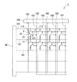
図1は、本実施形態の有機EL装置の配線構造を示す模式図であり、図1において符号1は有機EL装置である。
(First embodiment of organic EL device)
First, a first embodiment of the organic EL device of the present invention will be described.
FIG. 1 is a schematic diagram showing a wiring structure of the organic EL device of the present embodiment. In FIG. 1,
この有機EL装置1は、スイッチング素子として薄膜トランジスタ(Thin Film Transistor、以下TFTと称する。)を用いたアクティブマトリクス方式のもので、複数の走査線101…と、各走査線101に対して直角に交差する方向に延びる複数の信号線102…と、各信号線102に並列に延びる複数の電源線103…とからなる配線構成を有し、走査線101…と信号線102…との各交点付近に画素領域X…を形成したものである。
もちろん本発明の技術的思想に沿えば、TFTなどを用いるアクティブマトリクスは必須ではなく、単純マトリクス向けの素子基板を用いて本発明を実施し、単純マトリクス駆動しても全く同じ効果が低コストで得られる。
This
Of course, according to the technical idea of the present invention, an active matrix using TFT or the like is not indispensable. Even if the present invention is implemented using an element substrate for a simple matrix and the simple matrix is driven, the same effect can be obtained at low cost. can get.
信号線102には、シフトレジスタ、レベルシフタ、ビデオライン及びアナログスイッチを備えるデータ線駆動回路100が接続されている。また、走査線101には、シフトレジスタ及びレベルシフタを備える走査線駆動回路80が接続されている。
A data
さらに、画素領域Xの各々には、走査線101を介して走査信号がゲート電極に供給されるスイッチング用TFT(スイッチング素子)112と、このスイッチング用TFT112を介して信号線102から共有される画素信号を保持する保持容量113と、該保持容量113によって保持された画素信号がゲート電極に供給される駆動用TFT(スイッチング素子)123と、この駆動用TFT123を介して電源線103に電気的に接続したときに該電源線103から駆動電流が流れ込む陽極10と、該陽極10と陰極11との間に挟み込まれた発光層(有機発光層)12が設けられている。
Further, in each pixel region X, a switching TFT (switching element) 112 to which a scanning signal is supplied to the gate electrode via the
この有機EL装置1によれば、走査線101が駆動されてスイッチング用TFT112がオン状態になると、そのときの信号線102の電位が保持容量113に保持され、該保持容量113の状態に応じて、駆動用TFT123のオン・オフ状態が決まる。そして、駆動用TFT123のチャネルを介して、電源線103から陽極10に電流が流れ、さらに発光層12を介して陰極11に電流が流れる。発光層12は、これを流れる電流量に応じて発光する。
According to the
次に、本実施形態の有機EL装置1の具体的な態様を、図2〜図4を参照して説明する。ここで、図2は有機EL装置1の構成を模式的に示す平面図である。図3は有機EL装置1を模式的に示す断面図である。図4は、図3の要部(A部)を示す図であって、有機EL装置1の周辺部の構成を説明するための拡大断面図である。
Next, specific modes of the
まず、図2を参照し、有機EL装置1の構成を説明する。
図2は、基板本体20上に形成された前述した各種配線,TFT,各種回路によって、発光層12を発光させるTFT素子基板(以下「素子基板」という。)20Aを示す図である。
有機EL装置の素子基板20Aは、中央部分の実表示領域4(図2中二点鎖線枠内)と、実表示領域4の周囲に配置されたダミー領域5(一点鎖線および二点鎖線の間の領域)とを備えている。
First, the configuration of the
FIG. 2 is a diagram showing a TFT element substrate (hereinafter referred to as “element substrate”) 20 </ b> A that causes the
The
図1に示す画素領域Xからは、赤(R)、緑(G)または青(B)のいずれかの光が取り出され、図2に示す表示領域RGBが形成されている。実表示領域4においては、表示領域RGBがマトリクス状に配置されている。また、表示領域RGBの各々は、紙面縦方向において同一色で配列しており、いわゆるストライプ配置を構成している。そして、表示領域RGBが一つのまとまりとなって、表示単位画素が構成されており、該表示単位画素はRGBの発光を混色させてフルカラー表示を行うようになっている。 One of red (R), green (G), and blue (B) light is extracted from the pixel region X shown in FIG. 1, and the display region RGB shown in FIG. 2 is formed. In the actual display area 4, the display areas RGB are arranged in a matrix. In addition, each of the display areas RGB is arranged in the same color in the vertical direction of the paper, and constitutes a so-called stripe arrangement. The display area RGB is combined into one display unit pixel, and the display unit pixel mixes RGB light emission to perform full color display.
実表示領域4の図2中両側であってダミー領域5の下層側には、走査線駆動回路80、80が配置されている。また、実表示領域4の図2中上方側であってダミー領域5の下層側には、検査回路90が配置されている。この検査回路90は、有機EL装置1の作動状況を検査するための回路であって、例えば検査結果を外部に出力する検査情報出力手段(不図示)を備え、製造途中や出荷時における有機EL装置1の品質、欠陥の検査を行うことができるように構成されている。
Scan
(断面構造)
次に、図3を参照して、有機EL装置1の断面構造を説明する。
本実施形態における有機EL装置1は、いわゆる「トップエミッション構造」の有機EL装置である。トップエミッション構造は、光を素子基板側ではなく封止基板側から取り出すため、素子基板に配置された各種回路の大きさに影響されず、発光面積を広く確保できる効果がある。そのため、電圧及び電流を抑えつつ輝度を確保することが可能であり、発光素子の寿命を長く維持することができる。
この有機EL装置1は、陽極10と陰極11(一対の電極)の間に発光層12(有機発光層)を挟持した複数の発光素子21及び発光素子21を区切る画素隔壁13を有する素子基板20Aと、この素子基板20Aに対向配置された封止基板31と、が設けられている。
(Cross-section structure)
Next, a cross-sectional structure of the
The
The
(素子基板)
図3に示すように、有機EL装置1は、前述した各種配線(例えば、TFT等)が形成された素子基板20A上に、窒化珪素等からなる無機絶縁層14が被覆されている。また、無機絶縁層14にはコンタクトホール(不図示)が形成され、前述した陽極10が駆動用TFT123に接続されている。無機絶縁層14上にはアルミ合金等からなる金属反射板15が内装された平坦化層16が形成されている。
この平坦化層16上には、陽極10と陰極11が発光層12を挟持して形成され発光素子21として構成しているものである。また、この発光素子21を区分するように絶縁性の画素隔壁13が配置されている。
(Element board)
As shown in FIG. 3, in the
On the
本実施形態において、陽極10は、仕事関数が5eV以上の正孔注入層の高いITO(Indium Thin Oxide:インジウム錫酸化物)等の金属酸化物導電膜が用いられる。
なお、本実施形態においては、トップエミッション構造のため、陽極10は必ずしも光透過性を有する材料を用いる必要はなく、アルミ等からなる金属電極を用いてもよい。この構成を採用した場合は、前述した金属反射板15は設けなくてよい。
In the present embodiment, the
In the present embodiment, because of the top emission structure, the
陰極11を形成するための材料としては、本実施形態はトップエミッション構造であることから光透過性を有する材料である必要があり、したがって透明導電材料が用いられる。透明導電材料としては、ITOが好適とされるが、これ以外にも、例えば酸化インジウム・酸化亜鉛系アモルファス透明導電膜(Indium Zinc Oxide:IZO/アイ・ゼット・オー(登録商標))等を用いることができる。なお、本実施形態ではITOを用いるものとする。
As a material for forming the
また、陰極11は、電子注入効果の大きい(仕事関数が4eV以下)材料が好適に用いられる。例えば、カルシウムやマグネシウム、ナトリウム、リチウム金属、又はこれらの金属化合物である。金属化合物としては、フッ化カルシウム等の金属フッ化物や酸化リチウム等の金属酸化物、アセチルアセトナトカルシウム等の有機金属錯体が該当する。また、これらの材料だけでは、電気抵抗が大きく電極として機能しないため、発光部分を避けるようにアルミニウムや金、銀、銅などの金属層をパターン形成したり、ITOや酸化錫などの透明な金属酸化物導電層との積層体と組み合わせて用いてもよい。
なお、本実施形態では、フッ化リチウムとマグネシウム−銀合金、ITOの積層体を、透明性が得られる膜厚に調整して用いるものとする。
For the
In the present embodiment, a laminate of lithium fluoride, magnesium-silver alloy, and ITO is used by adjusting the film thickness to obtain transparency.
発光層12は、白色に発光する白色発光層を採用している。この白色発光層は、真空蒸着プロセスを用いて素子基板20Aの全面に形成されている。白色発光材料としては、スチリルアミン系発光材料,アントラセン系ドーパミント(青色)、或いはスチリルアミン系発光材料,ルブレン系ドーパミント(黄色)が用いられる。
なお、発光層12の下層或いは上層に、トリアリールアミン(ATP)多量体正孔注入層、TDP(トリフェニルジアミン)系正孔輸送層、アルミニウムキノリノール(Alq3)層(電子輸送層)を成膜することが好ましい。
The
A triarylamine (ATP) multimer hole injection layer, a TDP (triphenyldiamine) -based hole transport layer, and an aluminum quinolinol (Alq3) layer (electron transport layer) are formed on the lower layer or the upper layer of the light-emitting
また、素子基板20A上には、電極保護層17が形成され発光素子21及び画素隔壁13を被覆している。
この電極保護層17は、透明性や密着性、耐水性、ガスバリア性を考慮して珪素酸窒化物などの珪素化合物で構成することが望ましい。また、電極保護層17の膜厚は100nm以上が好ましく、画素隔壁13を被覆することで発生する応力によるクラック発生を防ぐため、膜厚の上限は200nm以下に設定することが好ましい。
なお、本実施形態においては、電極保護層17を単層で形成しているが、複数層で積層してもよい。例えば、低弾性率の下層と高耐水性の上層とで電極保護層17を構成してもよい。
An electrode
The electrode
In the present embodiment, the electrode
電極保護層17上には、有機緩衝層18が形成され電極保護層17を被覆している。
この有機緩衝層18は、画素隔壁13の形状の影響により、凹凸状に形成された電極保護層17の凹凸部分を埋めるように配置され、さらに、その上面は略平坦に形成される。有機緩衝層18は、素子基板20Aの反りや体積膨張により発生する応力を緩和し、不安定な形状の画素隔壁13からの電極保護層17の剥離を防止する機能を有する。また、有機緩衝層18の上面が略平坦化されるので、有機緩衝層18上に形成される硬い被膜からなる後述するガスバリア層19も平坦化される。したがって、応力が集中する部位がなくなり、これにより、ガスバリア層19でのクラックの発生を防止する。
An
The
有機緩衝層18は、硬化前の原料主成分としては、減圧雰囲気下でスクリーン印刷法により形成するために、流動性に優れ、かつ溶媒や揮発成分の無い、全てが高分子骨格の原料となる有機化合物材料である必要があり、好ましくはエポキシ基を有する分子量3000以下のエポキシモノマー/オリゴマーが用いられる(モノマーの定義:分子量1000以下、オリゴマーの定義:分子量1000〜3000)。例えば、ビスフェノールA型エポキシオリゴマーやビスフェノールF型エポキシオリゴマー、フェノールノボラック型エポキシオリゴマー、ポリエチレングリコールジグリシジルエーテル、アルキルグリシジルエーテル、3,4-エポキシシクロヘキセニルメチル-3',4'-エポキシシクロヘキセンカルボキシレート、ε-カプロラクトン変性3,4-エポキシシクロヘキシルメチル3',4'-エポキシシクロヘキサンカルボキレートなどがあり、これらが単独もしくは複数組み合わされて用いられる。
Since the
また、エポキシモノマー/オリゴマーと反応する硬化剤としては、電気絶縁性や接着性に優れ、かつ硬度が高く強靭で耐熱性に優れる硬化被膜を形成するものが良く、透明性に優れ、かつ硬化のばらつきの少ない付加重合型がよい。例えば、3−メチル−1,2,3,6−テトラヒドロ無水フタル酸、メチル−3,6−エンドメチレン−1,2,3,6−テトラヒドロ無水フタル酸、1,2,4,5−ベンゼンテトラカルボン酸二無水物、3,3',4,4'-ベンゾフェノンテトラカルボン酸二無水物などの酸無水物系硬化剤が好ましい。さらに、酸無水物の反応(開環)を促進する反応促進剤として1,6−ヘキサンジオールなど分子量が大きく揮発しにくいアルコール類やアミノフェノールなどのアミン化合物を微量添加することで低温硬化しやすくなる。これらの硬化は60〜100℃の範囲の加熱で行われ、その硬化被膜はエステル結合を持つ高分子となる。
また、硬化時間を短縮するためよく用いられるカチオン放出タイプの光重合開始剤を用いてもよいが、硬化収縮が急激に進まないよう反応の遅いものが良く、また、塗布後の加熱による粘度低下で平坦化を進めるように最終的には熱硬化を用いて硬化物を形成するものが好ましい。
Moreover, as the curing agent that reacts with the epoxy monomer / oligomer, one that forms a cured film with excellent electrical insulation and adhesiveness, high hardness, toughness, and excellent heat resistance, excellent transparency, and curing properties. An addition polymerization type with little variation is preferable. For example, 3-methyl-1,2,3,6-tetrahydrophthalic anhydride, methyl-3,6-endomethylene-1,2,3,6-tetrahydrophthalic anhydride, 1,2,4,5-benzene Acid anhydride curing agents such as tetracarboxylic dianhydride and 3,3 ′, 4,4′-benzophenonetetracarboxylic dianhydride are preferred. Furthermore, low-temperature curing is facilitated by adding trace amounts of amine compounds such as alcohols and aminophenols that have a high molecular weight and are difficult to volatilize such as 1,6-hexanediol as reaction accelerators that promote the reaction (ring opening) of acid anhydrides. Become. These curings are performed by heating in the range of 60 to 100 ° C., and the cured film becomes a polymer having an ester bond.
In addition, a cation-releasing photopolymerization initiator often used to shorten the curing time may be used, but it is preferable that the reaction is slow so that the curing shrinkage does not rapidly progress, and the viscosity decreases due to heating after coating. It is preferable to finally form a cured product using thermosetting so as to promote flattening.
さらに、電極保護層17やガスバリア層19との密着性を向上させるシランカップリング剤や、イソシアネート化合物などの捕水剤、硬化時の収縮を防ぐ微粒子などの添加物を混入しても良い。また、減圧雰囲気下で印刷形成するため、塗布した際に気泡が発生しにくくするために、含水量は100ppm以下に調整しておく。
Furthermore, additives such as a silane coupling agent that improves the adhesion to the electrode
これらの原料毎の粘度は、1000mPa・s(室温:25℃)以上が好ましい。塗布直後に発光層12へ浸透して、ダークスポットと呼ばれる非発光領域を発生させないためである。また、これらの原料を混合した緩衝層形成材料の粘度としては、500〜20000mPa・s、特に2000〜10000mPa・s(室温)が好ましい。
The viscosity of each raw material is preferably 1000 mPa · s (room temperature: 25 ° C.) or more. This is because it does not penetrate into the
また、有機緩衝層18の最適な膜厚としては、3〜10μmが好ましい。有機緩衝層18の膜厚が厚いほうが異物混入した場合等にガスバリア層19の欠陥を防ぐが、有機緩衝層18を合わせた層厚が10μmを超えると、後述する着色層37と発光層12の距離が広がり側面に逃げる光が増えるため光を取り出す効率が低下する。
また、硬化後の特性としては、有機緩衝層18の弾性率が1〜10GPaであることが好ましい。10GPa以上では、画素隔壁13上を平坦化した際の応力を吸収することができず、1GPa以下では耐摩耗性や耐熱性等が不足するためである。
Moreover, as an optimal film thickness of the
Moreover, as a characteristic after hardening, it is preferable that the elastic modulus of the
有機緩衝層18上には、有機緩衝層18を被覆し、かつ電極保護層17の終端部まで覆うような広い範囲で、ガスバリア層19が形成されている。
ガスバリア層19は、酸素や水分が浸入するのを防止するためのもので、これにより酸素や水分による発光素子21の劣化等を抑えることができる。ガスバリア層19は、透明性、ガスバリア性、耐水性を考慮して、好ましくは窒素を含む珪素化合物、すなわち珪素窒化物や珪素酸窒化物などによって形成される。
On the
The
ガスバリア層19の弾性率は、100GPa以上、具体的には200〜250GPa程度が好ましい。また、ガスバリア層19の膜厚は、200〜600nm程度が好ましい。200nm未満であると、異物に対する被覆性が不足し部分的に貫通孔が形成されてしまい、ガスバリア性が損なわれてしまうおそれがあるからであり、600nmを越えると、応力によるクラックが生じてしまうおそれがあるからである。
The elastic modulus of the
さらに、ガスバリア層19としては、積層構造としてもよいし、その組成を不均一にして特にその酸素濃度が連続的に、あるいは非連続的に変化するような構成としてもよい。なお、積層構造とした場合の膜厚は、第一ガスバリア層としては、200〜400nmが好ましく、200nm未満では有機緩衝層18の表面及び側面被覆が不足してしまう。異物等の被覆性を向上させる第二ガスバリア層としては、200〜800nmが好ましい。総厚1000nm以上を超えるとクラックの発生頻度が上がること及び経済的な面で好ましくない。
また、本実施形態では、有機EL装置1をトップエミッション構造としていることから、ガスバリア層19は光透過性を有する必要があり、したがってその材質や膜厚を適宜に調整することにより、本実施形態では可視光領域における光線透過率を例えば80%以上にしている。
Further, the
Further, in the present embodiment, since the
(封止基板)
さらに、ガスバリア層19が形成された素子基板20Aに封止基板31が対向配置されている。
この封止基板31は、発光光を取り出す表示面を有するため、ガラスまたは透明プラスチック(ポリエチレンテレフタレート、アクリル樹脂、ポリカーボネ―ト、ポリオレフィン等)などの光透過性を有する材料で構成されている。
(Sealing substrate)
Further, a sealing
Since the sealing
封止基板31の下面には、着色層37として赤色着色層37R、緑色着色層37G、青色着色層37Bがマトリクス状に配列形成されている。着色層37の周囲には、ブラックマトリクス層32が形成されている。
また、着色層37の各々は、陽極10上に形成された白色の発光層12に対向して配置されている。これにより、発光層12の発光光が、着色層37の各々を透過し、赤色光、緑色光、青色光の各色光として観察者側に出射するようになっている。さらに、額縁部からの光が漏洩しないように、周辺シール層33の幅内もブラックマトリックスが覆われている場合もある。
このように、有機EL装置1においては、発光層12の発光光を利用し、かつ、複数色の着色層37によってカラー表示を行うようになっている。
なお、封止基板31には、着色層37の他に、紫外線遮断、吸収層や、光反射防止膜、放熱層などの機能層を設けてもよい。
On the lower surface of the sealing
Further, each of the
As described above, in the
In addition to the
また、素子基板20Aと封止基板31との間の周辺部に周辺シール層33が設けられている。
この周辺シール層33は、素子基板20Aと封止基板31の貼り合わせの位置精度の向上と後述する充填層34(接着剤層)のはみ出しを防止する土手の機能を有し、紫外線によって硬化して粘度が向上するエポキシ材料等で構成されている。好ましくは、エポキシ基を有する分子量3000以下のエポキシモノマー/オリゴマーが用いられる(モノマーの定義:分子量1000以下、オリゴマーの定義:分子量1000〜3000)。例えば、ビスフェノールA型エポキシオリゴマーやビスフェノールF型エポキシオリゴマー、フェノールノボラック型エポキシオリゴマー、ポリエチレングリコールジグリシジルエーテル、アルキルグリシジルエーテル、3,4-エポキシシクロヘキセニルメチル-3',4'-エポキシシクロヘキセンカルボキシレート、ε-カプロラクトン変性3,4-エポキシシクロヘキシルメチル3',4'-エポキシシクロヘキサンカルボキレートなどがあり、これらが単独もしくは複数組み合わされて用いられる。
In addition, a
The
また、エポキシモノマー/オリゴマーと反応する硬化剤としては、ジアゾニウム塩、ジフェニルヨウドニウム塩、トリフェルスルフォニウム塩、スルホン酸エステル、鉄アレーン錯体、シラノール/アルミニウム錯体などのカチオン重合反応を起こす光反応型開始剤が好ましい。また、紫外線照射後に徐々に粘度が上昇する材料を用いると、1mm以下の細いシール幅でも周辺シール層33の断裂を防ぎ、貼り合わせ後の充填剤のはみ出しを防ぐことができる。また、貼り合わせ時に減圧した際に気泡が発生しにくくするため、含水量は1000ppm以下に調整された材料であることが好ましい。
Moreover, as a curing agent that reacts with an epoxy monomer / oligomer, a photoreactive type that causes a cationic polymerization reaction such as diazonium salt, diphenyliodonium salt, trifellsulfonium salt, sulfonate ester, iron arene complex, silanol / aluminum complex, etc. Initiators are preferred. In addition, when a material whose viscosity gradually increases after ultraviolet irradiation is used, the
周辺シール層33の膜厚としては、10〜25μmが好ましい。なお、素子基板20Aと封止基板31との距離を規制するために所定粒径の有機材料からなる球状粒子が混合されているものが好ましい。シール剤としては、通常、無機材料の燐片状や塊状の粒子を混合して粘度を高めているが、前述したガスバリア層19が貼り合わせ圧着時に損傷してしまうため、本実施形態における有機EL装置1は、弾性率が小さい有機材料の球状粒子を周辺シール層33に混合している。
The film thickness of the
また、素子基板20Aと封止基板31の間における周辺シール層33に囲まれた内部に、熱硬化性樹脂からなる充填層34(接着剤層)が形成されている。
この充填層34は、前述した周辺シール層33で囲まれた有機EL装置1の内部に隙間なく充填されており、素子基板20Aに対向配置された封止基板31を固定させ、かつ外部からの機械的衝撃に対して緩衝機能を有し、発光層12やガスバリア層19の保護をするものである。
A filling layer 34 (adhesive layer) made of a thermosetting resin is formed inside the
The filling
充填層34は、硬化前の原料主成分としては、流動性に優れ、かつ溶媒のような揮発成分を持たない有機化合物材料である必要があり、好ましくはエポキシ基を有する分子量3000以下のエポキシモノマー/オリゴマーが用いられる(モノマーの定義:分子量1000以下、オリゴマーの定義:分子量1000〜3000)。例えば、ビスフェノールA型エポキシオリゴマーやビスフェノールF型エポキシオリゴマー、フェノールノボラック型エポキシオリゴマー、ポリエチレングリコールジグリシジルエーテル、アルキルグリシジルエーテル、3,4-エポキシシクロヘキセニルメチル-3',4'-エポキシシクロヘキセンカルボキシレート、ε-カプロラクトン変性3,4-エポキシシクロヘキシルメチル3',4'-エポキシシクロヘキサンカルボキレートなどがあり、これらが単独もしくは複数組み合わされて用いられる。
The packed
また、エポキシモノマー/オリゴマーと反応する硬化剤としては、電気絶縁性に優れ、かつ強靭で耐熱性に優れる硬化皮膜を形成するものが良く、透明性に優れ、かつ硬化のばらつきの少ない付加重合型が良い。例えば、3−メチル−1,2,3,6−テトラヒドロ無水フタル酸、メチル−3,6−エンドメチレン−1,2,3,6−テトラヒドロ無水フタル酸、1,2,4,5−ベンゼンテトラカルボン酸二無水物、3,3’,4,4’−ベンゾフェノンテトラカルボン酸二無水物、またはそれらの重合物などの酸無水物系硬化剤が好ましい。これらの硬化は、60〜100℃の範囲で行われ、その硬化皮膜は珪素酸窒化物との密着性に優れるエステル結合を持つ高分子となる。さらに、酸無水の開環を促進する硬化促進剤として芳香族アミンやアルコール類、アミノフェノール等の比較的分子量の高いものを添加することで低温かつ短時間での硬化が可能となる。 Further, as the curing agent that reacts with the epoxy monomer / oligomer, an addition polymerization type that is excellent in electrical insulation, forms a cured film that is tough and excellent in heat resistance, has excellent transparency, and has little variation in curing. Is good. For example, 3-methyl-1,2,3,6-tetrahydrophthalic anhydride, methyl-3,6-endomethylene-1,2,3,6-tetrahydrophthalic anhydride, 1,2,4,5-benzene An acid anhydride curing agent such as tetracarboxylic dianhydride, 3,3 ′, 4,4′-benzophenone tetracarboxylic dianhydride, or a polymer thereof is preferable. These curings are performed in the range of 60 to 100 ° C., and the cured film becomes a polymer having an ester bond that is excellent in adhesion to silicon oxynitride. Furthermore, curing at a low temperature and in a short time is possible by adding a relatively high molecular weight material such as an aromatic amine, alcohol, aminophenol or the like as a curing accelerator that promotes ring opening of acid anhydride.
また、塗布時の粘度は、100〜1000mPa・s(室温)が好ましい。理由は、貼り合わせ後の空間への材料充填性を考慮したもので、加熱直後に一度粘度が下がってから硬化が始まる材料が好ましい。また、貼り合わせ時に減圧した際に気泡が発生しにくくするため、含水量は100ppm以下に調整された材料であることが好ましい。 The viscosity at the time of application is preferably 100 to 1000 mPa · s (room temperature). The reason is that the material filling property into the space after the bonding is taken into consideration, and a material in which the curing starts after the viscosity once decreases immediately after heating is preferable. Further, in order to make it difficult for bubbles to be generated when the pressure is reduced at the time of bonding, it is preferable that the water content is a material adjusted to 100 ppm or less.
充填層34の膜厚としては、5〜20μmが好ましい。なお、素子基板20Aと封止基板31との距離を規制するために所定粒径の有機材料からなる球状粒子が混合されているものが好ましい。また、前述した周辺シール層33と同様に、本実施形態における有機EL装置1は、弾性率が小さい有機材料の粒子を混合している。粒子に弾性率が小さい有機材料を充填層34に混合することにより、前述したガスバリア層19の損傷を防ぐことができる。
The film thickness of the
(周辺部の断面構造)
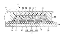
次に、図4を参照して有機EL装置1の周辺部の断面構造を説明する。
図4に示すように、この有機EL装置1の周辺部は、前述した素子基板20Aと封止基板31の間に、電極保護層17、有機緩衝層18、ガスバリア層19、周辺シール層33が順次積層される構成となっている。
有機緩衝層18の厚さは、中央部から周辺端部35にかけて小さくなっている。有機緩衝層18の周辺端部35における素子基板20Aの水平方向に対する仰角(接触角度)αは、20°以下で形成されることが好ましく、特に10°前後で形成されることが好ましい。これにより、有機緩衝層18を被覆するガスバリア層19の応力集中によるクラックや剥離等の損傷を防ぐことができる。
(Cross sectional structure of the periphery)
Next, a cross-sectional structure of the peripheral portion of the
As shown in FIG. 4, the periphery of the
The thickness of the
ここで、ガスバリア層19は、有機緩衝層18を完全に被覆するように有機緩衝層19よりも広く形成されており、このガスバリア層19上に周辺シール層33が配置されている。さらに、周辺シール層33の幅d内に有機緩衝層18の周辺端部35の立ち上がり部分36が位置するように形成されている。このように、前記有機緩衝層18の周辺端部35を覆うガスバリア層19を周辺シール層33により保護するため、ガスバリア層19の応力集中によるクラックや剥離等の損傷を防ぐことができる。これに伴って、水分がガスバリア層19を透過して発光素子21に到達することを防ぎ、ダークスポットの発生を防ぐことができる。
Here, the
なお、本実施形態におけるガスバリア層19は、周辺シール層33の外周より広く形成されているが、必ずしも周辺シール層33より広く形成する必要はない。つまり、ガスバリア層19の周辺端部38が、有機緩衝層19の周辺端部35よりも広く形成されていればよく、有機緩衝層19の周辺端部35と同様に周辺シール層33の幅d内に形成されていてもよい。また、電極保護層17の幅も有機緩衝層18より広く形成されており、通常、ガスバリア層19と同様のマスク材を使用して形成するため、ガスバリア層19と同じ幅で形成されている。
In addition, although the
また、この有機EL装置1の周辺部は額縁部(非発光部分)Dとなっている。この額縁部Dは、有機EL装置1の非発光部分であり、例えば、素子基板20A上の最端部に設けられた画素隔壁13から素子基板20Aの端部までの幅である。その額縁部Dは、例えば、2mmで形成され、周辺シール層の幅dは、例えば、1mmで形成されている。
The peripheral portion of the
上述の実施形態によれば、周辺シール層33をガスバリア層19上に配置したため、周辺シール層33をガスバリア層19の外側に配置する場合と比べて、額縁部Dの狭い有機EL装置1を得ることができるとともに、耐熱性や耐湿性に優れる有機EL装置1を形成できる。また、従来の缶封止構造に比べて、素子基板20A側と封止基板31側との接着面積が広いため、有機EL装置1の強度を維持したまま周辺シール層33の幅dを狭く形成することができる。そのため、非発光部分である額縁部Dを縮小させることができる。 したがって、携帯電話などの端末機器の小型化や、大型テレビ等の表示体のコンパクト化を図ることができ、デザインの自由度を向上させる効果がある。また、1枚のマザー基板から取れるパネル数も増やすことができ材料効率を向上させる効果がある。
According to the above-described embodiment, since the
また、一般的なシール剤の材料は、シール切れを防ぐために無機材料の粒子を混合して粘度を高めているが、周辺シール層33は、紫外線照射後から徐々に粘度上昇する材料からなることで、紫外線照射によって素子基板20A側と封止基板31側との貼り合わせ前に粘度を高めておくことができる。そのため、ディスペンサなどによる速い描画速度を維持しつつ、減圧貼り合わせ後のシール切れを防ぐことが出来る。
さらに、素子基板20Aと封止基板31の間における周辺シール層33に囲まれた内部に、熱硬化性樹脂からなる充填層34を形成することで、硬化収縮によるガスバリア層19以下の各機能層への影響を抑えつつ、素子基板20A側と封止基板31側との接着性を向上させる。そのため、素子基板20Aと封止基板31の間における周辺シール層33に囲まれた内部に、水分の侵入を防ぐことができる。また、封止基板31が固定され、かつ外部からの機械的衝撃に対して緩衝機能を有し、発光層12やガスバリア層19を保護することができる。
さらに、周辺シール層33と充填層34に有機材料の所定粒径の球状粒子を混合しているため、ガスバリア層19の損傷を防ぐとともに、素子基板20Aと封止基板31との距離を規制できる。そのため、発光層12から着色層37までの光路長を短く一定にすることができる。これにより、トップエミッション構造の場合には、発光層12から出射された光を、ブラックマトリクス層32に入射させることなく、封止基板31の外側に効率良く取り出すことが可能になる。したがって、有機EL装置1の輝度を向上させることができる。
In addition, in order to prevent the seal from being cut, a general sealant material is mixed with inorganic material particles to increase the viscosity. However, the
Furthermore, by forming a
Further, since spherical particles having a predetermined particle size of organic material are mixed in the
また、ガスバリア層19は、珪素化合物からなるため、透明性、ガスバリア性及び耐水性を確保することができる。
有機緩衝層18の周辺端部35における接触角度αは、20°以下に形成されているため、周辺端部35の立ち上がりを抑え、剥離を防止することができる。また、有機緩衝層18の周辺端部35を覆うガスバリア層19の凹凸を軽減することが可能になり、損傷を抑制することができる。
Moreover, since the
Since the contact angle α at the
(有機EL装置の製造方法)
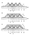
次に、図5,6を参照して本実施形態における有機EL装置1の製造方法を説明する。ここで、図5は、有機EL装置1の素子基板20A側の工程図であり、図6は、封止基板31側の工程図である。
(Method for manufacturing organic EL device)
Next, a method for manufacturing the
まず、図5(a)に示すように、陰極11までが積層された素子基板20Aに電極保護層17を形成する。
具体的には、例えば、窒素を含む珪素化合物、すなわち珪素窒化物や珪素酸窒化物などを、ECRスパッタ法やイオンプレーティング法等の高密度プラズマ成膜法により成膜する。
なお、透明無機材料としてのSiO2などの無機酸化物やLiFやMgF等のアルカリハライドを、真空蒸着法や高密度プラズマ成膜法により積層してもよい。
First, as shown in FIG. 5A, the electrode
Specifically, for example, a silicon compound containing nitrogen, that is, silicon nitride, silicon oxynitride, or the like is formed by a high-density plasma film forming method such as an ECR sputtering method or an ion plating method.
In addition, you may laminate | stack inorganic oxides, such as SiO2, as a transparent inorganic material, and alkali halides, such as LiF and MgF, by the vacuum evaporation method or the high-density plasma film-forming method.
次に、図5(b)に示すように、有機緩衝層18を電極保護層17上に形成する。
具体的には、減圧雰囲気下でスクリーン印刷を行った有機緩衝層18を、60〜100℃の範囲で加熱して硬化させる。この時点の問題点として、加熱直後に反応が開始されるまで一時的に粘度が低下する。この時に、有機緩衝層18の形成材料が電極保護層17や陰極11を透過してAlp3などの発光層12に浸透してダークスポットが発生する。そこで、ある程度硬化が進むまでは低温で放置し、ある程度高粘度化したところで温度を上げて完全硬化させることが好ましい。
Next, as shown in FIG. 5B, the
Specifically, the
次に、図5(c)に示すように、ガスバリア層19を有機緩衝層18上に形成する。
具体的には、ECRスパッタ法やイオンプレーティング法などの高密度プラズマ成膜法で形成する。また、形成前には、酸素プラズマ処理によって密着性を向上させると信頼性が向上する。
Next, as shown in FIG. 5C, the
Specifically, it is formed by a high density plasma film forming method such as an ECR sputtering method or an ion plating method. In addition, reliability is improved by improving the adhesion by oxygen plasma treatment before the formation.
一方、図6(a)に示すように、着色層37及びブラックマトリクス層32が形成された封止基板31の周辺部に周辺シール層33を形成する。
具体的には、ニードルディスペンス法により前述した紫外線硬化性樹脂材料を封止基板31の周囲に塗布していく。
なお、この塗布方法は、スクリーン印刷法を用いてもよい。
On the other hand, as shown in FIG. 6A, a
Specifically, the above-described ultraviolet curable resin material is applied around the sealing
Note that this printing method may be a screen printing method.
次に、図6(b)に示すように、封止基板31の周辺シール層33に囲まれた内部に充填層34を形成する。
具体的には、ジェットディスペンス法により前述した熱硬化性樹脂材料を塗布していく。
なお、この熱硬化性樹脂材料は、必ずしも封止基板31の全面に塗布する必要はなく、封止基板31上の複数箇所に塗布すればよい。
Next, as shown in FIG. 6B, a
Specifically, the thermosetting resin material described above is applied by a jet dispensing method.
The thermosetting resin material is not necessarily applied to the entire surface of the sealing
次に、図6(c)に示すように、周辺シール層33及び充填層34が塗布された封止基板31に紫外線照射を行う。
具体的には、周辺シール層33を仮硬化させる目的で、例えば、照度30MW/cm2 、光量2000MJ/cm2 の紫外線を封止基板31上に照射する。この時、紫外線硬化性樹脂である周辺シール層33のみが硬化され粘度が向上する。
Next, as shown in FIG. 6C, the sealing
Specifically, for the purpose of pre-curing the
次に、図5(c)に示す、ガスバリア層19までが形成された素子基板20A側と、図6(c)に示す、周辺シール層22が仮硬化された封止基板31とを貼り合わせる。この時、周辺シール層33が素子基板20A上に形成した有機緩衝層18の周辺端部35の立ち上がり部分36を完全に被覆するように配置する。
具体的には、この貼り合わせ工程は、真空度が例えば、1Paの真空雰囲気下で行い、加圧600Nで200秒間保持して圧着させる。
Next, the
Specifically, this bonding step is performed in a vacuum atmosphere with a degree of vacuum of, for example, 1 Pa, and held for 200 seconds at a pressure of 600 N for pressure bonding.
次に、圧着して貼り合わせた有機EL装置1を大気中で加熱する。
具体的には、素子基板20A側と封止基板31側を貼り合わせた状態で大気中において加熱することで、前述した仮硬化した周辺シール層33と、充填層34を熱硬化させる。 なお、素子基板20Aと封止基板31との間には真空の空間が存在しても、大気中で加熱硬化を行うことにより、充填層34がその空間に充填される。以上より、前述した本実施形態における所望の有機EL装置1を得ることができる。
Next, the
Specifically, by heating in the atmosphere with the
したがって、上述の製造方法によれば、素子基板20Aと封止基板31を貼り合わせる前に、周辺シール層33に紫外線照射し仮硬化させ、周辺シール層33の粘度を上昇させた後に素子基板30Aと封止基板31を貼り合わせる。そのため、塗布時には粘度が低いため高速で描画動作が行え、貼り合わせ時には粘度が上昇するため、貼り合わせ位置精度を向上させるとともに、充填層34のはみ出しを防ぐことができる。また、周辺シール層33を有機緩衝層18の周辺端部35の立ち上がり部分36上に形成することができる。さらに、封止基板31側の周辺シール層33の幅内が、額縁部Dの光漏洩防止としてブラックマトリックス層32による遮光がされている場合でも、貼り合わせ前に紫外線を照射することで周辺シール層33の硬化を進めることができる。
Therefore, according to the above-described manufacturing method, before the
また、素子基板20Aと封止基板31を貼り合わせた後に周辺シール33及び充填層34を加熱硬化させるため、位置精度を維持しつつ接着性及び耐熱性、耐湿性を向上させることができる。さらに、素子基板20Aと封止基板31を減圧下で貼り合わせ、大気中で硬化させるので、真空雰囲気下と大気中との差圧により、充填層34が周辺シール層33で囲まれた内部に隙間なく広がるため、気泡や水分の混入を防ぐことができる。
Further, since the
(有機EL装置の第2実施形態)
次に、本発明の第2実施形態における有機EL装置2について説明する。なお、本実施形態においては、第1実施形態と同一構成には同一符号を付して説明を省略する。ここで、図7は有機EL装置2を模式的に示す断面図である。図8は、図7の要部(B部)を示す図であって、有機EL装置2の周辺部の構成を説明するための断面図である。
(Second Embodiment of Organic EL Device)
Next, the
上述した第1実施形態における有機EL装置1は、トップエミッション構造であり、発光層12に白色発光層を用い、封止基板31に着色層37及びブラックマトリクス層32を有する構成であった。
本発明の第2実施形態における、有機EL装置2は、いわゆる「ボトムエミッション構造」であり、発光層12に赤色発光層12R、緑色発光層12Gおよび青色発光層12Bを用いている点が相違している。
The
The
図7に示すように、有機EL装置2は、前述した各種配線(例えば、TFT等)が形成され、窒化珪素等からなる無機絶縁層14に被覆された素子基板20Aを備えている。この素子基板20A上に、発光層12が、陽極10と陰極11の一対の電極に挟持されている。この発光層12は、無機絶縁層14上に形成された画素隔壁13により区切られ赤色発光層12R,緑色発光層12G,青色発光層12Bの発光層12が配列されている。
As shown in FIG. 7, the
本実施形態における発光層12を形成するための材料としては、蛍光あるいは燐光を発光することが可能な公知の発光材料が用いられる。また、赤色発光層12R、緑色発光層12G、青色発光層12Bを複数の陽極10毎に設けることでフルカラー表示が可能となる。
発光層12の形成材料として具体的には、高分子材料としては(ポリ)フルオレン誘導体(PF)、(ポリ)パラフェニレンビニレン誘導体(PPV)、ポリフェニレン誘導体(PP)、ポリパラフェニレン誘導体(PPP)、ポリビニルカルバゾール(PVK)、ポリチオフェン誘導体、ポリメチルフェニルシラン(PMPS)などのポリシラン系などが好適に用いられる。また、これらの高分子材料に、ペリレン系色素、クマリン系色素、ローダミン系色素などの高分子系材料や、ルブレン、ペリレン、9,10−ジフェニルアントラセン、テトラフェニルブタジエン、ナイルレッド、クマリン6、キナクリドン等の低分子材料をドープして用いることもできる。低分子材料としては、Alq3、DPVBiなどのホスト材料、これにナイルレッド、DCM、ルブレン、ぺリレン、ローダミンなどをドープして、またはホスト単独で、蒸着法にて用いることができる。
また、赤色発光層12Rの形成材料としては、例えばMEHPPV(ポリ(3−メトキシ6−(3−エチルヘキシル)パラフェニレンビニレン)を、緑色発光層12Gの形成材料としては、例えばポリジオクチルフルオレンとF8BT(ジオクチルフルオレンとベンゾチアジアゾールの交互共重合体)の混合溶液を、青色発光層12Bの形成材料としては、例えばポリジオクチルフルオレンを用いる場合がある。また、このような発光層12については、特にその厚さについては制限がなく、各色毎に好ましい膜厚が調整されている。
As a material for forming the
Specifically, the material for forming the
Further, as a material for forming the red
また、発光層12より上層部の構成は、第1実施形態と同様であるが、本実施形態ではボトムエミッション構造であることから、発光光を素子基板20A側から取り出すものである。そのため、上層部は、必ずしも光透過性を有する材料である必要はない。
The configuration of the upper layer portion from the
(周辺部の断面構造)
次に、図8を参照して有機EL装置2の周辺部の断面構造を説明する。
図8に示すように、有機EL装置2の周辺部は、第1実施形態と同様、有機緩衝層18の厚さは、中央部から周辺端部35にかけて小さくなっている。有機緩衝層18の周辺端部35における素子基板20Aの水平方向に対する仰角(接触角度)αは、20°以下で形成されることが好ましく、特に10°前後で形成されることが好ましい。これにより、有機緩衝層18を被覆するガスバリア層19の応力集中によるクラックや剥離等の損傷を防ぐことができる。
(Cross sectional structure of the periphery)
Next, a cross-sectional structure of the periphery of the
As shown in FIG. 8, the thickness of the
ここで、ガスバリア層19は、有機緩衝層18を完全に被覆するように有機緩衝層19よりも広く形成されており、このガスバリア層19上に周辺シール層33が配置されている。さらに、周辺シール層33の幅d内に有機緩衝層18の周辺端部35の立ち上がり部分36が位置するように形成されている。このように、前記有機緩衝層18の周辺端部35を覆うガスバリア層19を周辺シール層33により保護するため、ガスバリア層19の応力集中によるクラックや剥離等の損傷を防ぐことができる。これに伴って、水分がガスバリア層19を透過して発光素子21に到達することを防ぎ、ダークスポットの発生を防ぐことができる。
Here, the
なお、本実施形態におけるガスバリア層19は、周辺シール層33の外周より広く形成されているが、必ずしも周辺シール層33より広く形成する必要はない。つまり、ガスバリア層19の周辺端部38が、有機緩衝層19の周辺端部35よりも広く形成されていればよく、有機緩衝層19の周辺端部35と同様に周辺シール層33の幅d内に形成されていてもよい。また、電極保護層17の幅も有機緩衝層18より広く形成されており、通常、ガスバリア層19と同様のマスク材を使用して形成するため、ガスバリア層19と同じ幅で形成されている。
In addition, although the
また、この有機EL装置1の周辺部は額縁部(非発光部分)Dとなっている。この額縁部Dは、有機EL装置1の非発光部分であり、例えば、素子基板20A上の最端部に設けられた画素隔壁13から素子基板20Aの端部までの幅である。その額縁部Dは、例えば、2mmで形成され、周辺シール層の幅dは、例えば、1mmで形成されている。
The peripheral portion of the
上述した第2実施形態においても、第1実施形態と同様に、周辺シール層33をガスバリア層19上に配置したため、周辺シール層33をガスバリア層19の外側に配置する場合と比べて、額縁部Dの狭い有機EL装置1を得ることができるとともに、耐熱性や耐湿性に優れる有機EL装置1を形成できる。また、従来の缶封止構造に比べて、素子基板20A側と封止基板31側との接着面積が広いため、有機EL装置1の強度を維持したまま周辺シール層33の幅dを狭く形成することができる。そのため、非発光部分である額縁部Dを縮小させることができる。したがって、携帯電話などの端末機器の小型化や、大型テレビ等の表示体のコンパクト化を図ることができ、デザインの自由度を向上させる効果がある。また、1枚のマザー基板から取れるパネル数も増やすことができ材料効率を向上させる効果がある。
Also in the second embodiment described above, since the
また、一般的なシール剤の材料は、シール切れを防ぐために無機材料の粒子を混合して粘度を高めているが、周辺シール層33は、紫外線照射後から徐々に粘度上昇する材料からなることで、紫外線照射によって素子基板20A側と封止基板31側との貼り合わせ前に粘度を高めておくことができる。そのため、ディスペンサなどによる速い描画速度を維持しつつ、減圧貼り合わせ後のシール切れを防ぐことができる。
さらに、素子基板20Aと封止基板31の間における周辺シール層33に囲まれた内部に、熱硬化性樹脂からなる充填層34を形成することで、硬化収縮によるガスバリア層19以下の各機能層への影響を抑えつつ、素子基板20A側と封止基板31側との接着性を向上させる。そのため、素子基板20Aと封止基板31の間における周辺シール層33に囲まれた内部に、水分の侵入を防ぐことができる。また、封止基板31が固定され、かつ外部からの機械的衝撃に対して緩衝機能を有し、発光層12やガスバリア層19を保護することができる。
In addition, in order to prevent the seal from being cut, a general sealant material is mixed with inorganic material particles to increase the viscosity. However, the
Furthermore, by forming a
また、ガスバリア層19は、珪素化合物からなるため、透明性、ガスバリア性及び耐水性を確保することができる。
有機緩衝層18の周辺端部35における接触角度αは、20°以下に形成されているため、周辺端部35の立ち上がりを抑え、剥離を防止することができる。また、有機緩衝層18の周辺端部35を覆うガスバリア層19の凹凸を軽減することが可能になり、損傷を抑制することができる。
以上、本発明は、トップエミッション構造あるいはボトムエミッション構造に関らず効果がある。
Moreover, since the
Since the contact angle α at the
As described above, the present invention is effective regardless of the top emission structure or the bottom emission structure.
(電子機器)
次に、前記実施形態の有機EL装置を備えた電子機器の例について説明する。
図9(a)は、携帯電話の一例を示した斜視図である。図9(a)において、符号50は携帯電話本体を示し、符号51は有機EL装置を備えた表示部を示している。
図9(b)は、ワープロ、パソコンなどの携帯型情報処理装置の一例を示した斜視図である。図9(b)において、符号60は情報処理装置、符号61はキーボードなどの入力部、符号63は情報処理本体、符号62は有機EL装置を備えた表示部を示している。
図9(c)は、腕時計型電子機器の一例を示した斜視図である。図9(c)において、符号70は時計本体を示し、符号71は有機EL装置を備えたEL表示部を示している。
図9(a)〜(c)に示す電子機器は、先の実施形態に示した有機EL装置が備えられたものであるので、表示特性が良好な電子機器となる。
(Electronics)
Next, an example of an electronic apparatus including the organic EL device according to the embodiment will be described.
FIG. 9A is a perspective view showing an example of a mobile phone. In FIG. 9A,
FIG. 9B is a perspective view illustrating an example of a portable information processing apparatus such as a word processor or a personal computer. In FIG. 9B,
FIG. 9C is a perspective view showing an example of a wristwatch type electronic device. In FIG. 9C,
Since the electronic devices shown in FIGS. 9A to 9C are provided with the organic EL device described in the previous embodiment, the electronic devices have good display characteristics.
なお、電子機器としては、前記電子機器に限られることなく、種々の電子機器に適用することができる。例えば、ディスクトップ型コンピュータ、液晶プロジェクタ、マルチメディア対応のパーソナルコンピュータ(PC)及びエンジニアリング・ワークステーション(EWS)、ページャ、ワードプロセッサ、テレビ、ビューファインダ型又はモニタ直視型のビデオテープレコーダ、電子手帳、電子卓上計算機、カーナビゲーション装置、POS端末、タッチパネルを備えた装置等の電子機器に適用することができる。 The electronic device is not limited to the electronic device, and can be applied to various electronic devices. For example, a desktop computer, a liquid crystal projector, a multimedia personal computer (PC) and an engineering workstation (EWS), a pager, a word processor, a television, a viewfinder type or a monitor direct view type video tape recorder, an electronic notebook, an electronic The present invention can be applied to electronic devices such as a desktop computer, a car navigation device, a POS terminal, and a device having a touch panel.
1…有機EL装置 2…有機EL装置 10…陽極(一対の電極) 11…陰極(一対の電極) 12…発光層(有機発光層) 13…画素隔壁 14…無機絶縁層(絶縁層) 17…電極保護層(第1の無機膜) 18…有機緩衝層(有機膜) 19…ガスバリア層(第2の無機膜) 20A…素子基板(第1の基板) 21…発光素子 31…封止基板(第2基板) 33…周辺シール層 34…充填層(接着剤層) 35…周辺端部 123…駆動用TFT(トランジスタ)
DESCRIPTION OF
Claims (10)
前記第1の基板は、
トランジスタと、
前記トランジスタ上に設けられた絶縁層と、
前記絶縁層上に設けられ、第1の電極と第2の電極との間に発光層を有する発光素子と、
前記発光素子を覆うように設けられた第1の無機膜と、
前記第1の無機膜を覆うように設けられた有機膜と、
前記有機膜を覆うように設けられた第2の無機膜と、を含み、
前記周辺シール層は、前記発光素子の外側に設けられており、
前記絶縁層は、前記周辺シール層の外側まで延在するように設けられており、
前記有機膜の端部は、前記周辺シール層の配置領域内に位置しており、
前記第2の無機膜の端部は、前記周辺シール層の配置領域内には位置していないことを特徴とする有機エレクトロルミネッセンス装置。 A first substrate and a second substrate provided so as to face the first substrate are bonded together by a peripheral sealing layer provided between the first substrate and the second substrate. An organic electroluminescent device, comprising:
The first substrate is
A transistor,
An insulating layer provided on the transistor;
A light-emitting element provided on the insulating layer and having a light-emitting layer between the first electrode and the second electrode;
A first inorganic film provided to cover the light emitting element;
An organic film provided to cover the first inorganic film;
A second inorganic film provided so as to cover the organic film,
The peripheral seal layer is provided outside the light emitting element,
The insulating layer is provided so as to extend to the outside of the peripheral sealing layer,
The end of the organic film is located in the arrangement region of the peripheral seal layer,
The organic electroluminescence device according to claim 1, wherein an end portion of the second inorganic film is not located in an arrangement region of the peripheral sealing layer .
機膜と接触していることを特徴とする請求項1から請求項8のいずれか1項に記載の有機エレクトロルミネッセンス装置。 The organic material according to any one of claims 1 to 8, wherein the insulating layer is in contact with the first inorganic film in at least a part of an arrangement region of the peripheral sealing layer. Electroluminescence device.
えたことを特徴とする電子機器。 An electronic apparatus comprising the organic electroluminescence device according to any one of claims 1 to 9.
Priority Applications (1)
| Application Number | Priority Date | Filing Date | Title |
|---|---|---|---|
| JP2009116273A JP5012848B2 (en) | 2009-05-13 | 2009-05-13 | Organic electroluminescence device and electronic device |
Applications Claiming Priority (1)
| Application Number | Priority Date | Filing Date | Title |
|---|---|---|---|
| JP2009116273A JP5012848B2 (en) | 2009-05-13 | 2009-05-13 | Organic electroluminescence device and electronic device |
Related Parent Applications (1)
| Application Number | Title | Priority Date | Filing Date |
|---|---|---|---|
| JP2006234569A Division JP4337852B2 (en) | 2006-08-30 | 2006-08-30 | ORGANIC ELECTROLUMINESCENT DEVICE, ITS MANUFACTURING METHOD, AND ELECTRONIC DEVICE |
Publications (3)
| Publication Number | Publication Date |
|---|---|
| JP2009176756A JP2009176756A (en) | 2009-08-06 |
| JP2009176756A5 JP2009176756A5 (en) | 2009-09-17 |
| JP5012848B2 true JP5012848B2 (en) | 2012-08-29 |
Family
ID=41031589
Family Applications (1)
| Application Number | Title | Priority Date | Filing Date |
|---|---|---|---|
| JP2009116273A Expired - Fee Related JP5012848B2 (en) | 2009-05-13 | 2009-05-13 | Organic electroluminescence device and electronic device |
Country Status (1)
| Country | Link |
|---|---|
| JP (1) | JP5012848B2 (en) |
Families Citing this family (5)
| Publication number | Priority date | Publication date | Assignee | Title |
|---|---|---|---|---|
| JP2013109836A (en) | 2011-11-17 | 2013-06-06 | Mitsubishi Heavy Ind Ltd | Manufacturing method for organic el panel and sealing device for organic el panel |
| WO2015174318A1 (en) * | 2014-05-16 | 2015-11-19 | シャープ株式会社 | Sealing film, organic el element, and organic el display |
| KR102317715B1 (en) * | 2014-09-30 | 2021-10-25 | 엘지디스플레이 주식회사 | Organic light emitting display apparatus and manufacturing the same |
| JP6868904B2 (en) * | 2018-01-11 | 2021-05-12 | 株式会社Joled | Manufacturing method of organic EL display panel |
| JP7465652B2 (en) | 2019-12-05 | 2024-04-11 | JDI Design and Development 合同会社 | Self-luminous display panel and method for manufacturing same |
Family Cites Families (4)
| Publication number | Priority date | Publication date | Assignee | Title |
|---|---|---|---|---|
| JP3870796B2 (en) * | 2002-02-12 | 2007-01-24 | 松下電器産業株式会社 | Image processing apparatus and image processing method |
| JP4061588B2 (en) * | 2003-06-12 | 2008-03-19 | 富士電機ホールディングス株式会社 | Manufacturing method and manufacturing apparatus for organic EL display |
| JP2005116483A (en) * | 2003-10-10 | 2005-04-28 | Semiconductor Energy Lab Co Ltd | Semiconductor device and manufacturing method of the same |
| JP2006140003A (en) * | 2004-11-11 | 2006-06-01 | Seiko Epson Corp | Manufacturing method for display device, display device and electronic device |
-
2009
- 2009-05-13 JP JP2009116273A patent/JP5012848B2/en not_active Expired - Fee Related
Also Published As
| Publication number | Publication date |
|---|---|
| JP2009176756A (en) | 2009-08-06 |
Similar Documents
| Publication | Publication Date | Title |
|---|---|---|
| JP4337852B2 (en) | ORGANIC ELECTROLUMINESCENT DEVICE, ITS MANUFACTURING METHOD, AND ELECTRONIC DEVICE | |
| JP5119865B2 (en) | Organic electroluminescence equipment, electronic equipment | |
| JP2008066216A (en) | Organic electroluminescence device, its manufacturing method and electronic apparatus | |
| JP4329740B2 (en) | Method for manufacturing organic electroluminescent device and organic electroluminescent device | |
| US7915823B2 (en) | Organic electroluminescent device with surface-modifying layer, method for manufacturing the same, and electronic apparatus including the same | |
| JP4539547B2 (en) | LIGHT EMITTING DEVICE, LIGHT EMITTING DEVICE MANUFACTURING METHOD, AND ELECTRONIC DEVICE | |
| JP4631683B2 (en) | Light emitting device and electronic device | |
| JP4670875B2 (en) | Organic EL device | |
| JP2008059868A (en) | Organic electroluminescent device, its manufacturing method, and electronic apparatus | |
| JP2006222071A (en) | Light emitting device, manufacturing method thereof, and electronic equipment | |
| JP5240325B2 (en) | Organic electroluminescence device and electronic device | |
| JP2009048834A (en) | Organic electroluminescent device, manufacturing method thereof, and electronic equipment | |
| JP5056777B2 (en) | ORGANIC ELECTROLUMINESCENCE DEVICE, ITS MANUFACTURING METHOD, AND ELECTRONIC DEVICE | |
| JP2012216454A (en) | Light-emitting device and electronic apparatus | |
| JP2009134984A (en) | Organic electroluminescent device, and manufacturing method thereof | |
| JP2009199979A (en) | Organic electroluminescent device and its manufacturing method | |
| JP2010160906A (en) | Organic electroluminescent apparatus, method for manufacturing the same, and electronic device | |
| JP2009048835A (en) | Organic electroluminescent device and manufacturing method thereof, as well as electronic equipment | |
| JP5012848B2 (en) | Organic electroluminescence device and electronic device | |
| JP2008089634A (en) | Electro-optical device and electronic equipment | |
| JP2011018508A (en) | Electrooptic device and electronic equipment | |
| JP2009252687A (en) | Method for manufacturing of organic electroluminescent device, and the organic electroluminescent device | |
| JP2008123879A (en) | Method of manufacturing organic el device, and organic el device | |
| JP5741046B2 (en) | Electro-optical device, method of manufacturing electro-optical device, and electronic apparatus | |
| JP2015197995A (en) | Organic electroluminescence device manufacturing method and organic electroluminescence device |
Legal Events
| Date | Code | Title | Description |
|---|---|---|---|
| A521 | Request for written amendment filed |
Free format text: JAPANESE INTERMEDIATE CODE: A821 Effective date: 20090514 |
|
| A521 | Request for written amendment filed |
Free format text: JAPANESE INTERMEDIATE CODE: A523 Effective date: 20090717 |
|
| A621 | Written request for application examination |
Free format text: JAPANESE INTERMEDIATE CODE: A621 Effective date: 20090717 |
|
| A521 | Request for written amendment filed |
Free format text: JAPANESE INTERMEDIATE CODE: A821 Effective date: 20090721 |
|
| A131 | Notification of reasons for refusal |
Free format text: JAPANESE INTERMEDIATE CODE: A131 Effective date: 20111018 |
|
| A521 | Request for written amendment filed |
Free format text: JAPANESE INTERMEDIATE CODE: A523 Effective date: 20111219 |
|
| A521 | Request for written amendment filed |
Free format text: JAPANESE INTERMEDIATE CODE: A821 Effective date: 20111220 |
|
| RD04 | Notification of resignation of power of attorney |
Free format text: JAPANESE INTERMEDIATE CODE: A7424 Effective date: 20120127 |
|
| TRDD | Decision of grant or rejection written | ||
| A01 | Written decision to grant a patent or to grant a registration (utility model) |
Free format text: JAPANESE INTERMEDIATE CODE: A01 Effective date: 20120508 |
|
| A01 | Written decision to grant a patent or to grant a registration (utility model) |
Free format text: JAPANESE INTERMEDIATE CODE: A01 |
|
| A61 | First payment of annual fees (during grant procedure) |
Free format text: JAPANESE INTERMEDIATE CODE: A61 Effective date: 20120521 |
|
| FPAY | Renewal fee payment (event date is renewal date of database) |
Free format text: PAYMENT UNTIL: 20150615 Year of fee payment: 3 |
|
| R150 | Certificate of patent or registration of utility model |
Ref document number: 5012848 Country of ref document: JP Free format text: JAPANESE INTERMEDIATE CODE: R150 Free format text: JAPANESE INTERMEDIATE CODE: R150 |
|
| S531 | Written request for registration of change of domicile |
Free format text: JAPANESE INTERMEDIATE CODE: R313531 |
|
| R350 | Written notification of registration of transfer |
Free format text: JAPANESE INTERMEDIATE CODE: R350 |
|
| LAPS | Cancellation because of no payment of annual fees |