JP2011238928A - Lead frame for chip package, chip package, package module, and lighting system employing chip package module - Google Patents
Lead frame for chip package, chip package, package module, and lighting system employing chip package module Download PDFInfo
- Publication number
- JP2011238928A JP2011238928A JP2011104442A JP2011104442A JP2011238928A JP 2011238928 A JP2011238928 A JP 2011238928A JP 2011104442 A JP2011104442 A JP 2011104442A JP 2011104442 A JP2011104442 A JP 2011104442A JP 2011238928 A JP2011238928 A JP 2011238928A
- Authority
- JP
- Japan
- Prior art keywords
- terminal
- chip package
- light emitting
- chip
- package
- Prior art date
- Legal status (The legal status is an assumption and is not a legal conclusion. Google has not performed a legal analysis and makes no representation as to the accuracy of the status listed.)
- Pending
Links
- 229920005989 resin Polymers 0.000 claims description 31
- 239000011347 resin Substances 0.000 claims description 31
- 230000008878 coupling Effects 0.000 claims description 27
- 238000010168 coupling process Methods 0.000 claims description 27
- 238000005859 coupling reaction Methods 0.000 claims description 27
- OAICVXFJPJFONN-UHFFFAOYSA-N Phosphorus Chemical compound [P] OAICVXFJPJFONN-UHFFFAOYSA-N 0.000 claims description 18
- 230000000295 complement effect Effects 0.000 claims description 16
- 238000005286 illumination Methods 0.000 claims description 10
- 239000011810 insulating material Substances 0.000 claims description 8
- 238000005520 cutting process Methods 0.000 claims description 7
- 239000004020 conductor Substances 0.000 claims description 3
- 238000010586 diagram Methods 0.000 description 42
- 238000004519 manufacturing process Methods 0.000 description 20
- 230000004048 modification Effects 0.000 description 16
- 238000012986 modification Methods 0.000 description 16
- 238000000034 method Methods 0.000 description 9
- 230000008569 process Effects 0.000 description 7
- 239000000463 material Substances 0.000 description 5
- 239000003086 colorant Substances 0.000 description 4
- 238000009429 electrical wiring Methods 0.000 description 4
- 238000012858 packaging process Methods 0.000 description 4
- 239000004065 semiconductor Substances 0.000 description 4
- 150000001875 compounds Chemical class 0.000 description 3
- 238000001746 injection moulding Methods 0.000 description 3
- 229910052751 metal Inorganic materials 0.000 description 3
- 239000002184 metal Substances 0.000 description 3
- 238000009877 rendering Methods 0.000 description 3
- RYGMFSIKBFXOCR-UHFFFAOYSA-N Copper Chemical compound [Cu] RYGMFSIKBFXOCR-UHFFFAOYSA-N 0.000 description 2
- XUIMIQQOPSSXEZ-UHFFFAOYSA-N Silicon Chemical compound [Si] XUIMIQQOPSSXEZ-UHFFFAOYSA-N 0.000 description 2
- 229910052782 aluminium Inorganic materials 0.000 description 2
- XAGFODPZIPBFFR-UHFFFAOYSA-N aluminium Chemical compound [Al] XAGFODPZIPBFFR-UHFFFAOYSA-N 0.000 description 2
- 239000011248 coating agent Substances 0.000 description 2
- 238000000576 coating method Methods 0.000 description 2
- 229910052802 copper Inorganic materials 0.000 description 2
- 239000010949 copper Substances 0.000 description 2
- 239000003822 epoxy resin Substances 0.000 description 2
- 238000005530 etching Methods 0.000 description 2
- 230000017525 heat dissipation Effects 0.000 description 2
- 239000011159 matrix material Substances 0.000 description 2
- 150000004767 nitrides Chemical class 0.000 description 2
- 238000004806 packaging method and process Methods 0.000 description 2
- 239000004033 plastic Substances 0.000 description 2
- 229920000647 polyepoxide Polymers 0.000 description 2
- 238000003825 pressing Methods 0.000 description 2
- 238000009516 primary packaging Methods 0.000 description 2
- 238000009517 secondary packaging Methods 0.000 description 2
- 239000010703 silicon Substances 0.000 description 2
- 229910052710 silicon Inorganic materials 0.000 description 2
- -1 Ca A Al B O C N D Chemical compound 0.000 description 1
- BPQQTUXANYXVAA-UHFFFAOYSA-N Orthosilicate Chemical compound [O-][Si]([O-])([O-])[O-] BPQQTUXANYXVAA-UHFFFAOYSA-N 0.000 description 1
- 229910019142 PO4 Inorganic materials 0.000 description 1
- UCKMPCXJQFINFW-UHFFFAOYSA-N Sulphide Chemical compound [S-2] UCKMPCXJQFINFW-UHFFFAOYSA-N 0.000 description 1
- 230000015572 biosynthetic process Effects 0.000 description 1
- 230000008859 change Effects 0.000 description 1
- 238000009826 distribution Methods 0.000 description 1
- 230000000694 effects Effects 0.000 description 1
- 238000000605 extraction Methods 0.000 description 1
- 239000011521 glass Substances 0.000 description 1
- PCHJSUWPFVWCPO-UHFFFAOYSA-N gold Chemical compound [Au] PCHJSUWPFVWCPO-UHFFFAOYSA-N 0.000 description 1
- 239000010931 gold Substances 0.000 description 1
- 229910052737 gold Inorganic materials 0.000 description 1
- 238000002347 injection Methods 0.000 description 1
- 239000007924 injection Substances 0.000 description 1
- 238000009413 insulation Methods 0.000 description 1
- 239000004973 liquid crystal related substance Substances 0.000 description 1
- NBIIXXVUZAFLBC-UHFFFAOYSA-K phosphate Chemical compound [O-]P([O-])([O-])=O NBIIXXVUZAFLBC-UHFFFAOYSA-K 0.000 description 1
- 239000010452 phosphate Substances 0.000 description 1
- 239000000843 powder Substances 0.000 description 1
- 239000002096 quantum dot Substances 0.000 description 1
- 230000003252 repetitive effect Effects 0.000 description 1
- 150000003346 selenoethers Chemical class 0.000 description 1
- 230000035945 sensitivity Effects 0.000 description 1
- FVBUAEGBCNSCDD-UHFFFAOYSA-N silicide(4-) Chemical class [Si-4] FVBUAEGBCNSCDD-UHFFFAOYSA-N 0.000 description 1
- 238000005476 soldering Methods 0.000 description 1
- 239000000758 substrate Substances 0.000 description 1
- 238000005406 washing Methods 0.000 description 1
Images


Classifications
-
- H—ELECTRICITY
- H01—ELECTRIC ELEMENTS
- H01L—SEMICONDUCTOR DEVICES NOT COVERED BY CLASS H10
- H01L33/00—Semiconductor devices having potential barriers specially adapted for light emission; Processes or apparatus specially adapted for the manufacture or treatment thereof or of parts thereof; Details thereof
- H01L33/48—Semiconductor devices having potential barriers specially adapted for light emission; Processes or apparatus specially adapted for the manufacture or treatment thereof or of parts thereof; Details thereof characterised by the semiconductor body packages
- H01L33/62—Arrangements for conducting electric current to or from the semiconductor body, e.g. lead-frames, wire-bonds or solder balls
-
- H—ELECTRICITY
- H01—ELECTRIC ELEMENTS
- H01L—SEMICONDUCTOR DEVICES NOT COVERED BY CLASS H10
- H01L2224/00—Indexing scheme for arrangements for connecting or disconnecting semiconductor or solid-state bodies and methods related thereto as covered by H01L24/00
- H01L2224/01—Means for bonding being attached to, or being formed on, the surface to be connected, e.g. chip-to-package, die-attach, "first-level" interconnects; Manufacturing methods related thereto
- H01L2224/10—Bump connectors; Manufacturing methods related thereto
- H01L2224/15—Structure, shape, material or disposition of the bump connectors after the connecting process
- H01L2224/16—Structure, shape, material or disposition of the bump connectors after the connecting process of an individual bump connector
- H01L2224/161—Disposition
- H01L2224/16151—Disposition the bump connector connecting between a semiconductor or solid-state body and an item not being a semiconductor or solid-state body, e.g. chip-to-substrate, chip-to-passive
- H01L2224/16221—Disposition the bump connector connecting between a semiconductor or solid-state body and an item not being a semiconductor or solid-state body, e.g. chip-to-substrate, chip-to-passive the body and the item being stacked
- H01L2224/16245—Disposition the bump connector connecting between a semiconductor or solid-state body and an item not being a semiconductor or solid-state body, e.g. chip-to-substrate, chip-to-passive the body and the item being stacked the item being metallic
-
- H—ELECTRICITY
- H01—ELECTRIC ELEMENTS
- H01L—SEMICONDUCTOR DEVICES NOT COVERED BY CLASS H10
- H01L2224/00—Indexing scheme for arrangements for connecting or disconnecting semiconductor or solid-state bodies and methods related thereto as covered by H01L24/00
- H01L2224/01—Means for bonding being attached to, or being formed on, the surface to be connected, e.g. chip-to-package, die-attach, "first-level" interconnects; Manufacturing methods related thereto
- H01L2224/42—Wire connectors; Manufacturing methods related thereto
- H01L2224/47—Structure, shape, material or disposition of the wire connectors after the connecting process
- H01L2224/48—Structure, shape, material or disposition of the wire connectors after the connecting process of an individual wire connector
- H01L2224/4805—Shape
- H01L2224/4809—Loop shape
- H01L2224/48091—Arched
-
- H—ELECTRICITY
- H01—ELECTRIC ELEMENTS
- H01L—SEMICONDUCTOR DEVICES NOT COVERED BY CLASS H10
- H01L2224/00—Indexing scheme for arrangements for connecting or disconnecting semiconductor or solid-state bodies and methods related thereto as covered by H01L24/00
- H01L2224/01—Means for bonding being attached to, or being formed on, the surface to be connected, e.g. chip-to-package, die-attach, "first-level" interconnects; Manufacturing methods related thereto
- H01L2224/42—Wire connectors; Manufacturing methods related thereto
- H01L2224/47—Structure, shape, material or disposition of the wire connectors after the connecting process
- H01L2224/48—Structure, shape, material or disposition of the wire connectors after the connecting process of an individual wire connector
- H01L2224/481—Disposition
- H01L2224/48151—Connecting between a semiconductor or solid-state body and an item not being a semiconductor or solid-state body, e.g. chip-to-substrate, chip-to-passive
- H01L2224/48221—Connecting between a semiconductor or solid-state body and an item not being a semiconductor or solid-state body, e.g. chip-to-substrate, chip-to-passive the body and the item being stacked
- H01L2224/48245—Connecting between a semiconductor or solid-state body and an item not being a semiconductor or solid-state body, e.g. chip-to-substrate, chip-to-passive the body and the item being stacked the item being metallic
- H01L2224/48247—Connecting between a semiconductor or solid-state body and an item not being a semiconductor or solid-state body, e.g. chip-to-substrate, chip-to-passive the body and the item being stacked the item being metallic connecting the wire to a bond pad of the item
-
- H—ELECTRICITY
- H01—ELECTRIC ELEMENTS
- H01L—SEMICONDUCTOR DEVICES NOT COVERED BY CLASS H10
- H01L2924/00—Indexing scheme for arrangements or methods for connecting or disconnecting semiconductor or solid-state bodies as covered by H01L24/00
- H01L2924/10—Details of semiconductor or other solid state devices to be connected
- H01L2924/11—Device type
- H01L2924/12—Passive devices, e.g. 2 terminal devices
- H01L2924/1204—Optical Diode
- H01L2924/12044—OLED
-
- H—ELECTRICITY
- H01—ELECTRIC ELEMENTS
- H01L—SEMICONDUCTOR DEVICES NOT COVERED BY CLASS H10
- H01L2924/00—Indexing scheme for arrangements or methods for connecting or disconnecting semiconductor or solid-state bodies as covered by H01L24/00
- H01L2924/30—Technical effects
- H01L2924/301—Electrical effects
- H01L2924/3025—Electromagnetic shielding
-
- H—ELECTRICITY
- H01—ELECTRIC ELEMENTS
- H01L—SEMICONDUCTOR DEVICES NOT COVERED BY CLASS H10
- H01L33/00—Semiconductor devices having potential barriers specially adapted for light emission; Processes or apparatus specially adapted for the manufacture or treatment thereof or of parts thereof; Details thereof
- H01L33/48—Semiconductor devices having potential barriers specially adapted for light emission; Processes or apparatus specially adapted for the manufacture or treatment thereof or of parts thereof; Details thereof characterised by the semiconductor body packages
- H01L33/483—Containers
- H01L33/486—Containers adapted for surface mounting
Landscapes
- Engineering & Computer Science (AREA)
- Microelectronics & Electronic Packaging (AREA)
- Manufacturing & Machinery (AREA)
- Computer Hardware Design (AREA)
- Power Engineering (AREA)
- Led Device Packages (AREA)
- Fastening Of Light Sources Or Lamp Holders (AREA)
Abstract
Description
本発明は、複数のチップをパッケージングするのに使われるチップ・パッケージ用リードフレーム、チップ・パッケージ、パッケージ・モジュール及びパッケージ・モジュールを採用した照明装置に関する。 The present invention relates to a chip package lead frame used for packaging a plurality of chips, a chip package, a package module, and a lighting device employing the package module.
一般的にチップは、チップを保護して電気的配線を容易にする一次パッケージ過程を経た後、他の素子と共に回路を設けるために、回路基板に実装する二次パッケージング過程を経る。従って、チップを電子機器に使用するまでには、多段階のパッケージング過程を経ることによって、製造コストがかさんでしまう。 In general, a chip undergoes a primary packaging process for protecting the chip and facilitating electrical wiring, and then a secondary packaging process for mounting on a circuit board in order to provide a circuit together with other elements. Therefore, before the chip is used in an electronic device, the manufacturing cost is increased through a multi-stage packaging process.
例えば、一般的に、発光ダイオード(LED:light emitting diode)チップのような発光素子チップは、蛍光体やレンズなどをリードフレームに実装する一次パッケージング過程と、このように設けられた多数の発光素子チップを他の素子と共に回路を設けるために、回路基板に実装する二次パッケージング過程とを経た後、照明機器に使われる。LEDチップは、化合物半導体(compound semiconductor)のPN接合を介して発光源を構成することにより、多様な色の光を具現できる半導体素子であり、寿命が長く、小型化及び軽量化自在であり、光の指向性が強く、低電圧駆動が可能であるという長所がある。ところで、既存低価格の照明装置を代替して、かようなLEDのような発光素子チップの照明化のためには、その製造コストを低減させることができる方法が求められている。このために、材料費を低減し、かつ製造工程を単純化しようとする多くの研究が進められている。 For example, in general, a light emitting device chip such as a light emitting diode (LED) chip is a primary packaging process in which a phosphor or a lens is mounted on a lead frame, and a large number of light emitting devices provided in this manner. In order to provide a circuit with an element chip together with other elements, it is used in lighting equipment after undergoing a secondary packaging process for mounting on a circuit board. An LED chip is a semiconductor element that can realize light of various colors by configuring a light emitting source through a PN junction of a compound semiconductor, has a long life, and can be reduced in size and weight, There are advantages in that the directivity of light is strong and low voltage driving is possible. By the way, in order to replace the existing low-cost lighting device and to illuminate such a light emitting element chip such as an LED, a method capable of reducing the manufacturing cost is required. For this reason, many studies are underway to reduce material costs and simplify the manufacturing process.
本発明は、チップのパッケージ構造を改善し、パッケージ工程を単純化し、回路構成が容易なチップ・パッケージ用リードフレーム、チップ・パッケージ、パッケージ・モジュール及びパッケージ・モジュールを採用した照明装置を提供するものである。 The present invention provides a chip package lead frame, a chip package, a package module, and a lighting device employing the package module, which improves the package structure of the chip, simplifies the packaging process, and facilitates the circuit configuration. It is.
一類型によるチップ・パッケージ用リードフレームは、チップが搭載される搭載部と、搭載されるチップを外部に電気的に連結する端子部と、搭載部及び端子部を連結しつつ、チップが搭載された後で切断される複数の切断部と、を含み、端子部は、第1締結部が設けられた第1形状端子と、第1締結部に相補的に結合することができる第2締結部が設けられた第2形状端子と、を含む。 A chip package lead frame of the same type is mounted with a chip, a mounting part on which the chip is mounted, a terminal part for electrically connecting the mounted chip to the outside, and the mounting part and the terminal part are connected. A plurality of cutting portions that are cut after the second fastening portion, the terminal portion being a first shape terminal provided with the first fastening portion, and a second fastening portion that can be complementarily coupled to the first fastening portion. And a second shape terminal.
第1締結部及び第2締結部は、互いに噛み合う凹凸状になりうる。 The first fastening portion and the second fastening portion may be uneven so as to mesh with each other.
第1締結部及び第2締結部は、突起と、突起が挿入されうる締結溝と、からなりうる。 The first fastening portion and the second fastening portion may include a protrusion and a fastening groove into which the protrusion can be inserted.
搭載部は、複数のチップが搭載されうるように複数個設けられうる。 A plurality of mounting portions may be provided so that a plurality of chips can be mounted.
複数のチップを回路連結する複数の連結部を含むことができる。 A plurality of connecting parts for circuit connecting a plurality of chips may be included.
複数の連結部は、搭載される複数のチップ間を直列に連結させる少なくとも1つの中間連結部と、搭載される複数のチップのうち、直列回路の前端に位置したチップの第1電極に電気的に連結される第1連結部と、搭載される複数のチップのうち、直列回路の後端に位置したチップの第2電極に電気的に連結される第2連結部と、を含み、端子部は、第1連結部から延設された第1端子と、第2連結部から延設された第2端子と、を含むことができる。 The plurality of connecting portions are electrically connected to at least one intermediate connecting portion for connecting the plurality of mounted chips in series, and the first electrode of the chip located at the front end of the series circuit among the plurality of mounted chips. A first connection part connected to the second connection part, and a second connection part electrically connected to the second electrode of the chip located at the rear end of the series circuit among the plurality of chips to be mounted, and a terminal part Can include a first terminal extending from the first connecting portion and a second terminal extending from the second connecting portion.
第1連結部、中間連結部及び第2連結部は、一列配列され、第1端子は、複数の連結部の一列配列の前端側の第1前端子と、複数の連結部の一列配列の後端側の第1後端子と、を含み、第2端子は、複数の連結部の一列配列の前端側の第2前端子と、複数の連結部の一列配列の後端側の第2後端子と、を含むことができる。 The first connecting portion, the intermediate connecting portion, and the second connecting portion are arranged in a row, and the first terminal is arranged after the first front terminal on the front end side of the one row arrangement of the plurality of connecting portions and the one row arrangement of the plurality of connecting portions. A first rear terminal on the end side, and the second terminal is a second front terminal on the front end side of the one row arrangement of the plurality of connecting portions and a second rear terminal on the rear end side of the one row arrangement of the plurality of connecting portions. And can be included.
第1前端子及び第1後端子は、それぞれ第1形状端子及び第2形状端子であり、第2前端子及び第2後端子は、それぞれ第1形状端子及び第2形状端子でありうる。 The first front terminal and the first rear terminal may be a first shape terminal and a second shape terminal, respectively, and the second front terminal and the second rear terminal may be a first shape terminal and a second shape terminal, respectively.
第1前端子及び第1後端子は、それぞれ第1形状端子及び第2形状端子であり、第2前端子及び第2後端子は、それぞれ第2形状端子及び第1形状端子でありうる。 The first front terminal and the first rear terminal may be a first shape terminal and a second shape terminal, respectively, and the second front terminal and the second rear terminal may be a second shape terminal and a first shape terminal, respectively.
複数の連結部は、搭載される複数のチップそれぞれの第1電極を共通して連結する第1連結部と、搭載される複数のチップそれぞれの第2電極を共通して連結する第2連結部と、を含んで搭載される複数のチップを並列連結させることができる。 The plurality of connecting portions include a first connecting portion that commonly connects the first electrodes of each of the plurality of chips to be mounted, and a second connecting portion that commonly connects the second electrodes of each of the plurality of chips to be mounted. And a plurality of chips to be mounted can be connected in parallel.
他の類型によるチップ・パッケージは、チップ;チップが搭載される搭載部と、チップを外部に電気的に連結する端子部と、を含むリードフレーム;を含み、端子部は、第1締結部が設けられた第1形状端子と、第1締結部と相補的に結合することができる第2締結部が設けられた第2形状端子と、を含む。 A chip package according to another type includes a chip; a lead frame including a mounting portion on which the chip is mounted and a terminal portion that electrically connects the chip to the outside. The terminal portion includes a first fastening portion. A first shape terminal provided, and a second shape terminal provided with a second fastening portion that can be complementarily coupled to the first fastening portion.
第1締結部及び第2締結部は、互いに噛み合う凹凸状を有することができる。 The first fastening portion and the second fastening portion may have an uneven shape that meshes with each other.
第1締結部及び第2締結部は、それぞれ突起と、突起が挿入されうる締結溝と、を有することができる。 Each of the first fastening portion and the second fastening portion may have a protrusion and a fastening groove into which the protrusion can be inserted.
第1形状端子及び第2形状端子のうちいずれか一つは、リードフレームの厚みほど段差がつくように折れ曲がって形成されうる。 Any one of the first shape terminal and the second shape terminal may be formed to be bent so as to have a step as the thickness of the lead frame.
チップは、複数の発光素子チップを含み、搭載部は、複数の発光素子チップが搭載されるように複数個設けられ、リードフレームは、複数の発光素子チップを回路連結する複数の連結部を含むことができる。 The chip includes a plurality of light emitting element chips, a plurality of mounting portions are provided so that the plurality of light emitting element chips are mounted, and the lead frame includes a plurality of connecting portions for circuit connecting the plurality of light emitting element chips. be able to.
複数の連結部は、複数の発光素子チップ間を電気的に直列連結する中間連結部と、複数の発光素子チップのうちから直列回路の前端に位置した発光素子チップの第1電極と電気的に連結される第1連結部と、複数の発光素子チップのうちから直列回路の後端に位置した発光素子チップの第2電極と電気的に連結される第2連結部と、を含み、端子部は、第1連結部から延設された第1端子と、第2連結部から延設された第2端子と、を含むことができる。 The plurality of connecting portions are electrically connected to an intermediate connecting portion that electrically connects the plurality of light emitting element chips in series, and a first electrode of the light emitting element chip located at the front end of the series circuit among the plurality of light emitting element chips. A first connecting part to be connected; and a second connecting part electrically connected to a second electrode of the light emitting element chip located at the rear end of the series circuit among the plurality of light emitting element chips, and a terminal part Can include a first terminal extending from the first connecting portion and a second terminal extending from the second connecting portion.
複数の発光素子チップは、一列に配列されうる。このとき、第1端子は、複数の発光素子チップの一列配列の前端側の第1前端子と、複数の発光素子チップの一列配列の後端側の第1後端子と、を含み、第2端子は、複数の発光素子チップの一列配列の前端側の第2前端子と、複数の発光素子チップの一列配列の後端側の第2後端子と、を含み、連結部は、複数の発光素子の一列配列の一側に沿って、第1連結部から第1後端子に延設された第1延長部と、複数の発光素子の一列配列の他側に沿って、第2連結部から第2前端子に延設された第2延長部と、を含むことができる。 The plurality of light emitting element chips may be arranged in a line. At this time, the first terminal includes a first front terminal on the front end side of the one row arrangement of the plurality of light emitting element chips, and a first rear terminal on the rear end side of the one row arrangement of the plurality of light emitting element chips. The terminal includes a second front terminal on the front end side of the one-row arrangement of the plurality of light-emitting element chips and a second rear terminal on the rear end side of the one-row arrangement of the plurality of light-emitting element chips. A first extension extending from the first connection portion to the first rear terminal along one side of the one-row arrangement of the elements, and a second connection portion along the other side of the one-row arrangement of the plurality of light emitting elements. And a second extension portion extending to the second front terminal.
第1前端子及び第1後端子は、それぞれ第1形状端子及び第2形状端子であり、第2前端子及び第2後端子は、それぞれ第1形状端子及び第2形状端子でありうる。 The first front terminal and the first rear terminal may be a first shape terminal and a second shape terminal, respectively, and the second front terminal and the second rear terminal may be a first shape terminal and a second shape terminal, respectively.
第1前端子及び第1後端子は、それぞれ第1形状端子及び第2形状端子であり、第2前端子及び第2後端子は、それぞれ第2形状端子及び第1形状端子でありうる。 The first front terminal and the first rear terminal may be a first shape terminal and a second shape terminal, respectively, and the second front terminal and the second rear terminal may be a second shape terminal and a first shape terminal, respectively.
第1延長部の外側に、少なくとも1つの第3締結部が設けられ、第2延長部の外側に、少なくとも1つの第3締結部と相補的に結合することができる少なくとも1つの第4締結部が設けられうる。 At least one third fastening portion is provided on the outside of the first extension, and at least one fourth fastening portion can be complementarily coupled to the at least one third fastening portion on the outside of the second extension. Can be provided.
第1延長部及び第2延長部のそれぞれは、中間連結部と、絶縁性材質から形成された結合部材によって結合されうる。 Each of the first extension part and the second extension part may be coupled to the intermediate connection part by a coupling member formed of an insulating material.
結合部材は、第1延長部及び第2延長部の少なくとも一部分の外側まで延設されうる。 The coupling member may extend outside at least a portion of the first extension and the second extension.
結合部材は、発光素子チップから放出された光を反射させる反射キャビティと一体に形成されうる。 The coupling member may be integrally formed with a reflection cavity that reflects light emitted from the light emitting device chip.
発光素子チップから放出された光を反射させる反射キャビティをさらに含み、反射キャビティは、第1連結部、中間連結部及び第2連結部を相互結合させるように形成されうる。 The light emitting device chip may further include a reflection cavity that reflects light emitted from the light emitting device chip, and the reflection cavity may be formed to mutually couple the first connection part, the intermediate connection part, and the second connection part.
複数の連結部は、複数の発光素子チップそれぞれの第1電極を共通して連結する第1連結部と、複数の発光素子チップそれぞれの第2電極を共通して連結する第2連結部と、を含み、複数の発光素子チップを並列連結させ、端子部は、第1連結部から延びた第1端子と、第2連結部から延びた第2端子と、を含むことができる。 The plurality of connecting portions include a first connecting portion that commonly connects the first electrodes of the plurality of light emitting element chips, a second connecting portion that commonly connects the second electrodes of the plurality of light emitting element chips, The plurality of light emitting device chips may be connected in parallel, and the terminal portion may include a first terminal extending from the first connecting portion and a second terminal extending from the second connecting portion.
複数の発光素子チップは、一列に配列されうる。このとき、第1端子は、複数の発光素子チップの一列配列の前端側の第1前端子と、複数の発光素子チップの一列配列の後端側の第1後端子と、を含み、第2端子は、複数の発光素子チップの一列配列の前端側の第2前端子と、複数の発光素子チップの一列配列の後端側の第2後端子と、を含むことができる。 The plurality of light emitting element chips may be arranged in a line. At this time, the first terminal includes a first front terminal on the front end side of the one row arrangement of the plurality of light emitting element chips, and a first rear terminal on the rear end side of the one row arrangement of the plurality of light emitting element chips. The terminals may include a second front terminal on the front end side of the row arrangement of the plurality of light emitting element chips and a second rear terminal on the rear end side of the row arrangement of the plurality of light emitting element chips.
第1前端子及び第1後端子は、それぞれ第1形状端子及び第2形状端子であり、第2前端子及び第2後端子は、それぞれ第1形状端子及び第2形状端子でありうる。 The first front terminal and the first rear terminal may be a first shape terminal and a second shape terminal, respectively, and the second front terminal and the second rear terminal may be a first shape terminal and a second shape terminal, respectively.
第1前端子及び第1後端子は、それぞれ第1形状端子及び第2形状端子であり、第2前端子及び第2後端子は、それぞれ第2形状端子及び第1形状端子でありうる。 The first front terminal and the first rear terminal may be a first shape terminal and a second shape terminal, respectively, and the second front terminal and the second rear terminal may be a second shape terminal and a first shape terminal, respectively.
第1連結部の外側に、少なくとも1つの第3締結部が設けられ、第2連結部の外側に、少なくとも1つの第3締結部と相補的に結合することができる少なくとも1つの第4締結部が設けられうる。 At least one third fastening part is provided outside the first connection part, and at least one fourth fastening part can be complementarily coupled to the outside of the second connection part with at least one third fastening part. Can be provided.
第1連結部、中間連結部及び2連結部は、絶縁性材質から形成された結合部材に相互結合されうる。 The first connection part, the intermediate connection part, and the two connection parts may be mutually coupled to a coupling member made of an insulating material.
発光素子チップから放出された光を反射させる反射キャビティをさらに含み、反射キャビティは、第1連結部、中間連結部及び第2連結部を相互結合させるように形成されうる。 The light emitting device chip may further include a reflection cavity that reflects light emitted from the light emitting device chip, and the reflection cavity may be formed to mutually couple the first connection part, the intermediate connection part, and the second connection part.
複数の搭載部は、複数の連結部の一部に設けられうる。 The plurality of mounting portions can be provided in a part of the plurality of connecting portions.
複数の搭載部は、複数の連結部間に設けられ、複数の搭載部と複数の連結部は、絶縁性材質から形成された結合部材によって結合されうる。このとき、複数の搭載部は、熱伝導性材質によって形成できる。 The plurality of mounting portions are provided between the plurality of connecting portions, and the plurality of mounting portions and the plurality of connecting portions can be coupled by a coupling member formed of an insulating material. At this time, the plurality of mounting portions can be formed of a thermally conductive material.
複数の発光素子チップそれぞれは、複数の連結部にワイヤ・ボンディングされうる。 Each of the plurality of light emitting element chips may be wire bonded to the plurality of connecting portions.
複数の発光素子チップそれぞれは、複数の連結部にフリップチップ・ボンディングされうる。 Each of the plurality of light emitting device chips can be flip-chip bonded to the plurality of connecting portions.
複数の発光素子チップから放出された光を反射させる反射キャビティをさらに含むことができる。 A reflection cavity that reflects light emitted from the plurality of light emitting device chips may be further included.
複数の発光素子チップから放出された光を屈折させるレンズをさらに含むことができる。 A lens that refracts light emitted from the plurality of light emitting device chips may be further included.
複数の発光素子チップそれぞれは、GaN系発光ダイオードチップであって、蛍光体を含む透光性樹脂で塗布されうる。 Each of the plurality of light-emitting element chips is a GaN-based light-emitting diode chip and can be coated with a translucent resin including a phosphor.
さらに他の類型によるパッケージ・モジュールは、第1チップ・パッケージと第2チップ・パッケージとを含むものであり、第1チップ・パッケージ及び第2チップ・パッケージのそれぞれは、チップ;チップが搭載される搭載部と、チップを外部に電気的に連結する端子部と、を含むリードフレーム;を具備し、端子部は、第1締結部が設けられた第1形状端子と、第1締結部と相補的に結合することができる第2締結部が設けられた第2形状端子と、を含み、第1チップ・パッケージの第1形状端子は、第2チップ・パッケージの第2形状端子に電気的に連結されつつ相補的に結合する。 Still another type of package module includes a first chip package and a second chip package. Each of the first chip package and the second chip package includes a chip and a chip. A lead frame including a mounting portion and a terminal portion for electrically connecting the chip to the outside; and the terminal portion is complementary to the first shape terminal provided with the first fastening portion and the first fastening portion. A second shape terminal provided with a second fastening portion capable of being coupled to each other, wherein the first shape terminal of the first chip package is electrically connected to the second shape terminal of the second chip package. Complementary binding while being linked.
第1締結部及び第2締結部は、互いに噛み合う凹凸状を有することができる。 The first fastening portion and the second fastening portion may have an uneven shape that meshes with each other.
第1締結部及び第2締結部は、それぞれ突起と、突起が挿入されうる締結溝と、を有することができる。 Each of the first fastening portion and the second fastening portion may have a protrusion and a fastening groove into which the protrusion can be inserted.
チップは、複数の発光素子チップを含み、搭載部は、複数の発光素子チップが搭載されうるように複数個設けられ、リードフレームは、複数の発光素子チップを回路連結する複数の連結部を含むことができる。 The chip includes a plurality of light emitting element chips, the plurality of mounting portions are provided so that the plurality of light emitting element chips can be mounted, and the lead frame includes a plurality of connecting portions for circuit connecting the plurality of light emitting element chips. be able to.
複数の連結部は、複数の発光素子チップ間を電気的に直列連結する中間連結部と、複数の発光素子チップのうち直列回路の前端に位置した発光素子チップの第1電極と電気的に連結される第1連結部と、複数の発光素子チップのうち直列回路の後端に位置した発光素子チップの第2電極と電気的に連結される第2連結部と、を含み、端子部は、第1連結部から延設された第1端子と、第2連結部から延設された第2端子と、を含むことができる。 The plurality of connecting portions are electrically connected to an intermediate connecting portion that electrically connects the plurality of light emitting element chips in series and a first electrode of the light emitting element chip located at the front end of the series circuit among the plurality of light emitting element chips. And a second connection part that is electrically connected to the second electrode of the light emitting element chip located at the rear end of the series circuit among the plurality of light emitting element chips, and the terminal part includes: The 1st terminal extended from the 1st connection part and the 2nd terminal extended from the 2nd connection part can be included.
複数の発光素子チップは、一列に配列され、第1端子は、複数の発光素子チップの一列配列の前端側の第1前端子と、複数の発光素子チップの一列配列の後端側の第1後端子と、を含み、第2端子は、複数の発光素子チップの一列配列の前端側の第2前端子と、複数の発光素子チップの一列配列の後端側の第2後端子と、を含み、連結部は、複数の発光素子の一列配列の一側に沿って、第1連結部から第1後端子に延設された第1延長部と、複数の発光素子の一列配列の他側に沿って、第2連結部から第2前端子に延設された第2延長部と、を含むことができる。 The plurality of light emitting element chips are arranged in a row, and the first terminal is a first front terminal on the front end side of the row arrangement of the plurality of light emitting element chips, and a first terminal on the rear end side of the row arrangement of the plurality of light emitting element chips. A second terminal, a second front terminal on the front end side of the row arrangement of the plurality of light emitting element chips, and a second rear terminal on the rear end side of the row arrangement of the plurality of light emitting element chips. The connecting portion includes a first extension portion extending from the first connecting portion to the first rear terminal along one side of the one-row arrangement of the plurality of light-emitting elements, and the other side of the one-row arrangement of the plurality of light-emitting elements. , And a second extension part extending from the second connection part to the second front terminal.
第1前端子及び第1後端子は、それぞれ第1形状端子及び第2形状端子であり、第2前端子及び第2後端子は、それぞれ第1形状端子及び第2形状端子であり、第1チップ・パッケージの第1後端子は、第2チップ・パッケージの第1前端子に電気的に連結されつつ相補的に結合し、第1チップ・パッケージの第2後端子は、第2チップ・パッケージの第2前端子に電気的に連結されつつ相補的に結合し、第1チップ・パッケージと第2チップ・パッケージとが、複数の発光素子チップの一列配列方向に連結されうる。 The first front terminal and the first rear terminal are a first shape terminal and a second shape terminal, respectively. The second front terminal and the second rear terminal are a first shape terminal and a second shape terminal, respectively. The first rear terminal of the chip package is complementarily coupled to the first front terminal of the second chip package while being electrically connected, and the second rear terminal of the first chip package is the second chip package. The first chip package and the second chip package can be connected in a line arrangement direction of the plurality of light emitting device chips.
第1前端子及び第1後端子は、それぞれ第1形状端子及び第2形状端子であり、第2前端子及び第2後端子は、それぞれ第2形状端子及び第1形状端子であり、第1チップ・パッケージの第1後端子は、第2チップ・パッケージの第1前端子に電気的に連結されつつ相補的に結合し、第1チップ・パッケージの第2後端子は、第2チップ・パッケージの第2前端子に電気的に連結されつつ相補的に結合し、第1チップ・パッケージと第2チップ・パッケージとが、複数の発光素子チップの一列配列方向に連結されうる。 The first front terminal and the first rear terminal are a first shape terminal and a second shape terminal, respectively. The second front terminal and the second rear terminal are a second shape terminal and a first shape terminal, respectively. The first rear terminal of the chip package is complementarily coupled to the first front terminal of the second chip package while being electrically connected, and the second rear terminal of the first chip package is the second chip package. The first chip package and the second chip package can be connected in a line arrangement direction of the plurality of light emitting device chips.
第1延長部の外側に、少なくとも1つの第3締結部が設けられ、第2延長部の外側に、少なくとも1つの第3締結部と相補的に結合することができる少なくとも1つの第4締結部が設けられ、第1チップ・パッケージの第4締結部が、第2チップ・パッケージの第3締結部に電気的に連結されつつ相補的に結合され、第1チップ・パッケージと第2チップ・パッケージとが、複数の発光素子チップの一列配列に垂直一方向に連結されうる。 At least one third fastening portion is provided on the outside of the first extension, and at least one fourth fastening portion can be complementarily coupled to the at least one third fastening portion on the outside of the second extension. And the fourth fastening portion of the first chip package is complementarily coupled to the third fastening portion of the second chip package while being electrically connected to each other, and the first chip package and the second chip package. Can be connected in a vertical direction to a single row array of a plurality of light emitting device chips.
複数の連結部は、複数の発光素子チップそれぞれの第1電極を共通して連結する第1連結部と、複数の発光素子チップそれぞれの第2電極を共通して連結する第2連結部と、を含み、複数の発光素子チップを並列連結させ、端子部は、第1連結部から延びた第1端子と、第2連結部から延びた第2端子と、を含むことができる。 The plurality of connecting portions include a first connecting portion that commonly connects the first electrodes of the plurality of light emitting element chips, a second connecting portion that commonly connects the second electrodes of the plurality of light emitting element chips, The plurality of light emitting device chips may be connected in parallel, and the terminal portion may include a first terminal extending from the first connecting portion and a second terminal extending from the second connecting portion.
複数の発光素子チップは、一列に配列され、第1端子は、複数の発光素子チップの一列配列の前端側の第1前端子と、複数の発光素子チップの一列配列の後端側の第1後端子と、を含み、第2端子は、複数の発光素子チップの一列配列の前端側の第2前端子と、複数の発光素子チップの一列配列の後端側の第2後端子と、を含むことができる。 The plurality of light emitting element chips are arranged in a row, and the first terminal is a first front terminal on the front end side of the row arrangement of the plurality of light emitting element chips, and a first terminal on the rear end side of the row arrangement of the plurality of light emitting element chips. A second terminal, a second front terminal on the front end side of the row arrangement of the plurality of light emitting element chips, and a second rear terminal on the rear end side of the row arrangement of the plurality of light emitting element chips. Can be included.
第1前端子及び第1後端子は、それぞれ第1形状端子及び第2形状端子であり、第2前端子及び第2後端子は、それぞれ第1形状端子及び第2形状端子であり、第1チップ・パッケージの第1後端子は、第2チップ・パッケージの第1前端子に電気的に連結されつつ相補的に結合し、第1チップ・パッケージの第2後端子は、第2チップ・パッケージの第2前端子に電気的に連結されつつ相補的に結合し、第1チップ・パッケージと第2チップ・パッケージとが、複数の発光素子チップの一列配列方向に連結されうる。 The first front terminal and the first rear terminal are a first shape terminal and a second shape terminal, respectively. The second front terminal and the second rear terminal are a first shape terminal and a second shape terminal, respectively. The first rear terminal of the chip package is complementarily coupled to the first front terminal of the second chip package while being electrically connected, and the second rear terminal of the first chip package is the second chip package. The first chip package and the second chip package can be connected in a line arrangement direction of the plurality of light emitting device chips.
第1前端子及び第1後端子は、それぞれ第1形状端子及び第2形状端子であり、第2前端子及び第2後端子は、それぞれ第2形状端子及び第1形状端子であり、第1チップ・パッケージの第1後端子は、第2チップ・パッケージの第1前端子に電気的に連結されつつ相補的に結合し、第1チップ・パッケージの第2後端子は、第2チップ・パッケージの第2前端子に電気的に連結されつつ相補的に結合し、第1チップ・パッケージと第2チップ・パッケージとが、複数の発光素子チップの一列配列方向に連結されうる。 The first front terminal and the first rear terminal are a first shape terminal and a second shape terminal, respectively. The second front terminal and the second rear terminal are a second shape terminal and a first shape terminal, respectively. The first rear terminal of the chip package is complementarily coupled to the first front terminal of the second chip package while being electrically connected, and the second rear terminal of the first chip package is the second chip package. The first chip package and the second chip package can be connected in a line arrangement direction of the plurality of light emitting device chips.
第1連結部の外側に、少なくとも1つの第3締結部が設けられ、第2連結部の外側に、少なくとも1つの第3締結部と相補的に結合することができる少なくとも1つの第4締結部が設けられ、第1チップ・パッケージの第4締結部が、第2チップ・パッケージの第3締結部に電気的に連結されつつ相補的に結合され、第1チップ・パッケージと第2チップ・パッケージとが、複数の発光素子チップの一列配列に垂直一方向に連結されうる。 At least one third fastening part is provided outside the first connection part, and at least one fourth fastening part can be complementarily coupled to the outside of the second connection part with at least one third fastening part. And the fourth fastening portion of the first chip package is complementarily coupled to the third fastening portion of the second chip package while being electrically connected to each other, and the first chip package and the second chip package. Can be connected in a vertical direction to a single row array of a plurality of light emitting device chips.
さらに他の類型による照明装置は、前述のパッケージ・モジュールと、パッケージ・モジュールに電源を供給する電源供給部と、を含むことができる。 Still another type of lighting device may include the aforementioned package module and a power supply unit that supplies power to the package module.
電源供給部は、電源を入力されるインターフェースと、照明モジュールに供給される電源を制御する電源制御部と、を含むことができる。 The power supply unit may include an interface to which power is input and a power control unit that controls the power supplied to the lighting module.
かような照明装置は、パッケージ・モジュールが非自発光表示装置に光を照明するバックライト・ユニットでありうる。 Such an illumination device may be a backlight unit in which a package module illuminates a non-self light emitting display device.
本発明によれば、リードフレームの構造を改善することによって、チップ・パッケージを直接的に連結してモジュール化することにより、かようなパッケージ・モジュールを採用する装置の製造コストを低減させることができる。 According to the present invention, by improving the structure of the lead frame, the chip package is directly connected to be modularized, thereby reducing the manufacturing cost of a device employing such a package module. it can.
以下、添付された図面を参照しつつ、本発明の実施形態について詳細に説明する。図面で同じ参照符号は、同じ構成要素を指し、各構成要素の大きさや厚みは、説明の明瞭性のために誇張されていることがある。 Hereinafter, embodiments of the present invention will be described in detail with reference to the accompanying drawings. In the drawings, the same reference numerals indicate the same components, and the size and thickness of each component may be exaggerated for clarity of explanation.
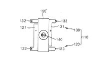
図1は、本発明の一実施形態によるチップ・パッケージの概略的な平面図であり、図2は、図1のチップ・パッケージのA−A’線に沿って切り取った概略的な側断面図である。 FIG. 1 is a schematic plan view of a chip package according to an embodiment of the present invention, and FIG. 2 is a schematic cross-sectional side view taken along line AA ′ of the chip package of FIG. It is.
図1及び図2を参照すれば、本実施形態のチップ・パッケージ100は、発光素子チップ140、発光素子チップ140を外部に電気的に連結するリードフレーム110、及び発光素子チップ140から放出される光を反射させ、外部にガイドする反射キャビティ150を含む。
Referring to FIGS. 1 and 2, the
リードフレーム110は、アルミニウム、銅のような伝導性を有した金属プレートが、プレス加工、エッチング加工などを介して形成されうる。かようなリードフレーム110は、互いに分離された第1フレーム部120と、第2フレーム部130とを含み、それら分離された第1フレーム部120と、第2フレーム部130は、絶縁性樹脂からなる反射キャビティ150によって結合固定される。
The
第1フレーム部120は、第1連結部121と、第1前端子(front terminal)122と、第1後端子(rear terminal)123とを含む。第1連結部121は、発光素子チップ140の負極に連結される。一方、第1前端子122は、第1連結部121から前端側に延設され、第1後端子123は、第1連結部121から後端側に延設される。
The
第2フレーム部130は、第2連結部131と、第2前端子132と、第2後端子133とを含む。第2連結部131は、発光素子チップ140の正極に連結される。第2前端子132は、第2連結部131から前端側に延設され、第2後端子133は、第2連結部131から後端側に延設される。第1連結部121及び第2連結部131は所定ギャップGほど離隔されている。第2連結部131には、発光素子チップ140が搭載される搭載部139が設けられる。本実施形態のチップ・パッケージ100は、リードフレーム110の搭載部139に、発光素子チップ140が直接搭載されるチップ・オン・リードフレーム(chip on lead-frame)構造のパッケージである。搭載部139には、複数の発光素子チップ140の接合を容易にするボンディング・パッド(図示せず)が付着されもする。場合によっては、搭載部139が第1連結部121側に設けられもする。
The
第1前端子122と第2前端子132は、チップ・パッケージ100の前端に位置し、負極端子及び正極端子になり、第1後端子123と第2後端子133は、チップ・パッケージ100の後端に位置し、負極端子及び正極端子になり、チップ・パッケージ100の端子部をなす。本実施形態は、説明の便宜のために、第1フレーム部120に負極が連結され、第2フレーム部130に正極が連結されると説明しているが、正極と負極は、発光素子チップ140の配線方向によって変わりうる。
The
第1前端子122と第2前端子132は、第1締結部が設けられた端子であり、第1後端子123と第2後端子133は、第2締結部が設けられた端子である。第1締結部と第2締結部は、互いに噛み合って相補的に結合することができる凹凸状を有する。すなわち、第1前端子122と第2前端子132は、凹型に入り込んだ長方形の第1締結部を有する形状端子であり、第1後端子123と第2後端子133は、凸型に突き出た長方形の第2締結部を有する形状端子である。
The
発光素子チップ140は、2電極を有する素子であり、正極と負極とを具備した発光ダイオード・チップ(light emitting diode chip)でありうる。発光ダイオード・チップは、発光ダイオード・チップをなす化合物半導体の材質によって、青色、緑色、赤色などを発光させることができる。さらに、発光ダイオード・チップの表面に蛍光コーティングを施し、白色光などの多様な色相の光を発光させることもできる。
The light emitting
例えば、青色発光ダイオード・チップは、GaNとInGaNとが交互に形成された複数の量子ウェル層構造の活性層を有することができ、かような活性層の上下部に、AlXGaYNZの化合物半導体で形成されたP型クラッド層とN型クラッド層とが形成されうる。その以外に、韓国特許出願第2010−015422号や同第2010−018259号に開示された発光ダイオード・チップが、本実施形態の発光素子チップとして使われうる。 For example, a blue light emitting diode chip may have an active layer having a plurality of quantum well layer structures in which GaN and InGaN are alternately formed, and Al X Ga Y N Z may be formed above and below the active layer. A P-type clad layer and an N-type clad layer made of the compound semiconductor can be formed. In addition, the light-emitting diode chips disclosed in Korean Patent Application Nos. 2010-015422 and 2010-018259 can be used as the light-emitting element chip of the present embodiment.
本実施形態は、発光素子チップ140が発光ダイオード・チップである場合について説明しているが、これに限定されるものではない。例えば、発光素子チップ140は、UV(ultraviolet)光ダイオード・チップ、レーザダイオード・チップ、有機発光ダイオード・チップでありうる。
In the present embodiment, the case where the light emitting
反射キャビティ150は、発光素子チップ140を取り囲んだ形態で、第1連結部121及び第2連結部131にわたって形成される。かような反射キャビティ150は、発光素子チップ140から放出される光を反射面150aで反射させ、所定の角度範囲で出射させ、発光素子チップ140から放出される光の外部への抽出効率を向上させる。反射キャビティ150は、エポキシ樹脂、シリコン樹脂、プラスチックのような絶縁性樹脂でもって射出工程を介して形成されうる。
The
反射キャビティ150の内部空間には、発光素子チップ140が実装された後、発光素子チップ140を保護するように、透光性樹脂160で充填されうる。さらに、透光性樹脂160には蛍光体が含まれ、所定の蛍光光を放出させることができる。例えば、発光素子チップ140が、青色発光ダイオード・チップや紫外線(UV)光ダイオード・チップである場合、透光性樹脂160に、黄色、赤色及び緑色の蛍光体粉末を含め、白色光を放出させることができる。かような蛍光体は、酸化物系蛍光体、窒化物系蛍光体、硫化物系蛍光体、ケイ酸塩系蛍光体、ホスフェート系蛍光体、セレン化物系蛍光体であり、それ以外に、量子点(quantum dot)を利用した蛍光体でありうる。具体的な例として、緑黄色蛍光体として、YAG系蛍光体、緑色蛍光体として、CaAAlBOCNDのような窒化物系蛍光体、赤色蛍光体として、(Ba,Sr)XSiYOZのようなシリサイド系列蛍光体などがある。
The internal space of the
一方、反射キャビティ150は、第1連結部121及び第2連結部131にわたって形成されるので、反射キャビティ150によって、第1連結部121及び第2連結部131が固設される。
Meanwhile, since the
リードフレーム110で、発光素子チップ140の電気的連結のための部分や端子部を除外した残りの部分には、絶縁性材質がコーティングされ、絶縁膜(図示せず)を形成することもできる。かような絶縁膜は、反射キャビティ150と同一材質によって形成され、反射キャビティ150の形成時に共に形成されもする。
An insulating material (not shown) may be formed on the
図3は本実施形態のチップ・パッケージを並列連結したパッケージ・モジュールを図示し、図4は、図3に図示されたパッケージ・モジュールの回路図である。 FIG. 3 illustrates a package module in which the chip packages of the present embodiment are connected in parallel. FIG. 4 is a circuit diagram of the package module illustrated in FIG.
本実施形態のパッケージ・モジュールは、第1チップ・パッケージ100Aと、第2チップ・パッケージ100Bとを含み、それら第1チップ・パッケージ100Aと第2チップ・パッケージ100Bとが、相互間に直接的に機構的及び回路的に連結された構造を有する。第1チップ・パッケージ100Aと第2チップ・パッケージ100Bは、それぞれ図1及び図2を参照して説明したチップ・パッケージである。
The package module of the present embodiment includes a first chip package 100A and a
前述のように、第1チップ・パッケージ100Aと第2チップ・パッケージ100Bは、端子部自体に締結構造が設けられ、直接的に連結するのである。すなわち、第1チップ・パッケージ100Aの第1後端子123Aの凸型の第2締結部は、第2チップ・パッケージ100Bの第1前端子123Bの凹型の第1締結部に挿入され、第1チップ・パッケージ100Aの第2後端子133Aの凸型の第2締結部は、第2チップ・パッケージ100Bの第2前端子133Bの凹型の第1締結部に挿入されることによって、第1チップ・パッケージ100Aと第2チップ・パッケージ100Bは、機構的であって電気的に連結される。このとき、第1チップ・パッケージ100Aの発光素子チップ140Aの負極は、第2チップ・パッケージ100Bの発光素子チップ140Bの負極と共通に連結され、第1チップ・パッケージ100Aの発光素子チップ140Aの正極は、第2チップ・パッケージ100Bの発光素子チップ140Bの正極と共通に連結されるので、本実施形態のパッケージ・モジュールは、図4に図示されているように、第1チップ・パッケージ100Aと第2チップ・パッケージ100Bとが並列連結された構造を有する。
As described above, the first chip package 100A and the
かような本実施形態のパッケージ・モジュールは、別途の基板に実装したり、ハンダ付けなどの固定を経なくとも、チップ・パッケージ同士直接に連結でき、両端に露出された端子部を介して、ソケットやそれ以外の多様な形式のコネクタに挿入され、直ちに照明装置の照明モジュールとして使われうる。 The package module of this embodiment can be directly connected to each other without being mounted on a separate substrate or fixed by soldering or the like, via terminal portions exposed at both ends, It can be inserted into a socket or other types of connectors and used immediately as a lighting module of a lighting device.
端子部に設けられた締結構造は、多様な変形例が可能である。図5A及び図5Bは、図1のチップ・パッケージの第1形状端子及び第2形状端子の変形例である。変形例のチップ・パッケージ100’,100”は、端子部の締結構造を除いては、前述の実施形態のチップ・パッケージ100と同一である。
Various modifications can be made to the fastening structure provided in the terminal portion. 5A and 5B are modifications of the first shape terminal and the second shape terminal of the chip package of FIG. The modified
図5Aを参照すれば、一変形例のチップ・パッケージ100’は、第1前端子122’と第2前端子132’は、それぞれ凸型の第2締結部及び凹型の第1締結部を有し、第1後端子123’と第2後端子133’は、それぞれ凹型の第1締結部及び凸型の第2締結部を有する。図1及び図2を参照しつつ説明したチップ・パッケージ100は、第1前端子122及び第2前端子132の二つとも同じ形状の締結構造(すなわち、第1締結部)を有し、第1後端子123及び第2後端子133もやはり、同じ形状の締結構造(すなわち、第2締結部)を有しているという点で、本変形例と違いがある。本変形例のチップ・パッケージ100’は、チップ・パッケージ100’の前端及び後端のそれぞれに、相補的な第1締結部及び第2締結部がいずれも設けられることによって、チップ・パッケージ100’が、前端同士あるいは後端同士で結合されうる(図23参照)。
Referring to FIG. 5A, in a modified
図5Bを参照すれば、他の変形例のチップ・パッケージ100”は、第1前端子122”と第2前端子132”は、逆三角形の形状に凹型の第1締結部を有し、第1後端子123”と第2後端子133”は、逆三角形の形状に凸型の第2締結部を有する。図1及び図2を参照しつつ説明したチップ・パッケージ100の場合、第1締結部は、長方形の形状に凹型であり、第2締結部は、長方形の形状に凸型であるという点で、本変形例と違いがある。本変形例のチップ・パッケージ100”は、逆三角形の形状の第1締結部及び第2締結部が互いに噛み合って結合された後には、長手方向に外れない。図5Bでは、第1締結部及び第2締結部が逆三角形の形状に、凹型、凸型である場合を例に挙げて図示しているが、多様な相補的形状が可能である。
Referring to FIG. 5B, in another modified
一方、図1及び図2を参照しつつ説明したチップ・パッケージ100は、発光素子チップ140が反射キャビティ150内でワイヤ・ボンディングされた場合を例に挙げて説明したが、これに限定されるものではない。
On the other hand, the
図6Aないし図6Dは、前述の実施形態の発光素子チップ実装の多様な変形例を図示している。 6A to 6D illustrate various modifications of the light emitting element chip mounting of the above-described embodiment.
図6Aを参照すれば、発光素子チップ140の収容される反射キャビティ150上には、レンズ170がさらに設けられうる。レンズ170は、発光素子チップ140から放出される光を集束させたり発散させ、配光分布を適切に設計できるようにする。かようなレンズ170は、透明樹脂やガラスなどから形成され、反射キャビティ150上に直接形成したり、別途に形成した後で付着させることができる。透光性樹脂160とレンズ170は、一体に形成されもする。レンズ170がさらに設けられるという点を除いては、前述の実施形態と実質的に同一であるので、重複する説明は省略する。
Referring to FIG. 6A, a
前述の実施形態では、反射キャビティ150が設けられた場合を例に挙げて説明しているが、これに限定されるものではない。図6Bや図6Cに図示されているように、反射キャビティが省略されもする。
In the above-described embodiment, the case where the
図6Bは、透光性樹脂161が、ワイヤ・ボンディングされた発光素子チップ140に、反射キャビティなしに直接に塗布される場合を図示する。かような透光性樹脂161には、多様な蛍光体が添加され、白色やその他の蛍光色を放出させることもできる。さらに、蛍光体を含む透光性樹脂161は、複数層に塗布されて形成されうる。例えば、透光性樹脂161の最初層には、赤色蛍光体が添加され、2番目の層には、緑色蛍光体が添加されうるのである。
FIG. 6B illustrates a case where the
さらに、図示されているように、透光性樹脂161の上には、レンズ171がさらに設けられ、発光素子チップ140から放出された光の集束または発散を調節することができるのである。透光性樹脂161とレンズ171は、一体に形成されもする。
Further, as shown in the drawing, a
図6Cは、発光素子チップ140’が、リードフレーム110にフリップチップ・ボンディングされた場合を図示している。この場合、発光素子チップ140’は、リードフレーム110に、金のような導電性材質のバンプ(bump)45,46で接合されつつ電気的に連結される。一方、かようなフリップチップ・ボンディングの場合、発光素子チップ140’は、接合された面の反対側面を介して、光が放出される。フリップチップ・ボンディングされた発光素子チップ140’の上部には、透光性樹脂162でコーティングされうる。かような透光性樹脂162には、蛍光体が分散されもする。透光性樹脂162は、フィルム状で発光素子チップ140’の上部を覆うこともできる。さらに、透光性樹脂162の上には、レンズ172がさらに設けられうる。
FIG. 6C illustrates a case where the light emitting
図6Bや図6Cに図示された場合のように反射キャビティがない場合、リードフレーム110の第1連結部121及び第2連結部131は、透光性樹脂161,162やレンズ171,172で結合され、または別途の結合部材(図示せず)を介して固設されうる。
When there is no reflective cavity as shown in FIGS. 6B and 6C, the first connecting
前述の実施形態では、発光素子チップ140,140’が搭載される搭載部139(図2)が、連結部121,131に設けられた場合を例に挙げて説明しているが、これに限定されるものではない。図6Dを参照すれば、リードフレーム110’は、所定空間を形成する折曲部110’aを有し、折曲部110’aによって設けられた空間に、折曲部110’aに離隔された状態でヒートスラッグ(heat slug)118が配されて、かようなヒートスラッグ118は、リードフレーム110’に、固定部材119を介して固設される。ヒートスラッグ118が、発光素子チップ140が搭載される搭載部になる。すなわち、発光素子チップ140は、ヒートスラッグ118に付着され、ワイヤ141,142を介して、リードフレーム110’の折曲部110’aに電気的に連結される。ヒートスラッグ118は、熱伝導性が良好な金属から形成され、発光素子チップ140で発生する熱を放出する通路となる。一方、搭載された発光素子チップ140は、透光性樹脂163でコーティングされ、かような透光性樹脂162には、蛍光体が含まれうる。さらに、反射キャビティ150’によって取り囲まれ、上部には、レンズ173が設けられうる。本変形例は、ヒートスラッグ118を利用して、放熱性を向上させているが、それ以外の多様な公知の放熱構造が採用されうるのである。
In the above-described embodiment, the mounting portion 139 (FIG. 2) on which the light emitting element chips 140 and 140 ′ are mounted is described as an example, but the present invention is not limited thereto. Is not to be done. Referring to FIG. 6D, the
図1及び図2を参照しつつ説明した実施形態のチップ・パッケージ100や、図6Bや図6Cを参照しつつ説明した変形例では、反射キャビティ150(図2)や、透光性樹脂160,161,162によって区画された領域に、1つの発光素子チップ140が実装された場合を例に挙げて説明しているが、複数の発光素子チップが共に実装されうる。たとえば、同じ色の光を放出する発光素子チップを共に実装して光量を上げたり、互いに異なる色の光を放出する発光素子チップを共に実装して、演色性を高めることもできる。このように、複数の発光素子チップが共に実装される場合であるならば、それらチップは、ウェーハレベルで相互間に配線されたり、あるいはリードフレーム110に付着された後に多様な公知の方式で、直列及び/または並列に配線されうる。一方、発光素子チップ140の保護のために、ツェナーダイオード(Zener diode)チップが共に実装されもする。
In the
図1及び図2を参照しつつ説明したチップ・パッケージ100の反射キャビティ150は、第1連結部121及び第2連結部131にわたって形成されるが、これに限定されるものではない。図7は、図1のチップ・パッケージの反射キャビティの変形例を図示している。
The
本変形例の反射キャビティ150’は、連結部121及び第2連結部131の外側を覆い包んで形成される。すなわち、反射キャビティ150’は、リードフレーム110の外郭まで形成されることによって、第1連結部121及び第2連結部131だけではなく、第1連結部121から長く延設された第1後端子123や、第2連結部131から長く延設された第2前端子132まで覆い包んで固設させることができる。さらに、反射キャビティ150’が、リードフレーム110の外側を覆うことによって、チップ・パッケージの絶縁性を向上させることができる。かような反射キャビティ150’は、リードフレーム110を覆い包んだ形態に形成されたり、リードフレーム110の上部にだけ設けられうる。
The
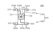
図8は、本発明の他の実施形態によるチップ・パッケージの概略的な平面図であり、図9A及び図9Bは、図8のチップ・パッケージの第1フレーム部及び第2フレーム部の概略的な側断面図である。本実施形態のチップ・パッケージ200は、リードフレーム210に設けられた締結構造を除いては、前述の実施形態のチップ・パッケージ100と実質的に同一である。発光素子チップ140の実装構造や反射キャビティ150の構造は、前述の実施形態及び変形例で説明された構造が適用されうる。
FIG. 8 is a schematic plan view of a chip package according to another embodiment of the present invention, and FIGS. 9A and 9B are schematic views of a first frame part and a second frame part of the chip package of FIG. FIG. The
図8、図9A及び図9Bを参照すれば、本実施形態のチップ・パッケージ200は、発光素子チップ140、発光素子チップ140を外部に電気的に連結するリードフレーム210、及び発光素子チップ140から放出される光を反射させ、外部にガイドする反射キャビティ150を含む。リードフレーム210は、互いに分離された第1フレーム部220と、第2フレーム部230とを含み、それら分離された第1フレーム部220と、第2フレーム部230は、絶縁性樹脂からなる反射キャビティ150によって結合固定される。
Referring to FIGS. 8, 9A, and 9B, the
第1フレーム部220は、第1連結部221と、第1前端子222と、第1後端子223とを含む。第1連結部221は、発光素子チップ140の負極に連結される。一方、第1前端子222は、第1連結部221から前端側に延設され、第1後端子223は、第1連結部221から後端側に延設される。第2フレーム部230は、第2連結部231と、第2前端子232と、第2後端子233とを含む。第2連結部231は、発光素子チップ140の正極に連結される。第2前端子232は、第2連結部231から前端側に延設され、第2後端子233は、第2連結部231から後端側に延設される。
The
第1前端子222及び第2前端子232は、それぞれ第1締結部及び第2締結部が設けられ、第1後端子223及び第2後端子233は、それぞれ第2締結部及び第1締結部が設けられた端子である。第1締結部は、少なくとも1つの突起222a,233aからなり、第2締結部は、少なくとも1つの突起222a,233aに相応する締結溝232a,223aからなる。突起222a,233aは、反射キャビティ150の形成時に、共に絶縁性樹脂で射出成形されて形成されたり、チップ・パッケージング工程中に、リードフレーム210をプレス加工し、突起状に突出させて形成させることができる。
The
かような突起222a,233aと締結溝232a,223aは、リードフレーム210を重ねつつ締結する。従って、チップ・パッケージ200の結合時、リードフレーム210の歪みを抑制するために、第1前端子222、第2前端子232、第1後端子223及び第2後端子233のうち、一部が段差がつくように曲折させることができる。例えば、図9A及び図9Bに図示されているように、締結溝232a,223aが形成される第1後端子223及び第2前端子232には、高さHほど高く段差をつけた折曲部223b,232bが設けられうる。このとき高さHは、リードフレーム210の厚みTと同じにすることができる。
The
本実施形態は、締結溝232a,223aが形成される第1後端子223及び第2前端子232を曲折させたが、これに限定されるものではない。たとえば、突起222a,233aが形成された第1前端子222及び第2後端子233を、高さHほど低く段差がつくように曲折させることもできるのである。
In the present embodiment, the first
本実施形態のチップ・パッケージ200は、突起222a,233aと締結溝232a,223aとが、チップ・パッケージ200の前端及び後端にいずれも存在する場合を図示しているが、これに限定されるものではない。たとえば、第1前端子222及び第2前端子232には、突起222a,233aのみ設けられ、第1後端子223及び第2後端子233には、締結溝232a,223aのみ設けられうるのである。
The
図10は、図8のチップ・パッケージを並列連結したパッケージ・モジュールを図示し、図11A及び11Bは、図10のパッケージ・モジュールの結合構造を図示する側断面図である。 10 illustrates a package module in which the chip packages of FIG. 8 are connected in parallel, and FIGS. 11A and 11B are side cross-sectional views illustrating the coupling structure of the package module of FIG.
本実施形態のパッケージ・モジュールは、第1チップ・パッケージ200Aと、第2チップ・パッケージ200Bとを含み、それら第1チップ・パッケージ200Aと第2チップ・パッケージ200Bとが、相互間に直接的に機構的及び回路的に連結された構造を有している。第1チップ・パッケージ200A及び第2チップ・パッケージ200Bのそれぞれは、図8、図9A及び図9Bを参照しつつ説明したチップ・パッケージ200である。
The package module of the present embodiment includes a first chip package 200A and a
第2チップ・パッケージ200Bの第1前端子223Bの突起222Baは、第1チップ・パッケージ200Aの第1後端子223Aの締結溝223Aaに挿入され、第1チップ・パッケージ200Aの第2後端子233Aの突起233Aaは、第2チップ・パッケージ200Bの第2前端子233Bの締結溝233Aaに挿入されることによって、第1チップ・パッケージ200Aと第2チップ・パッケージ200Bは、機構的であって電気的に連結される。このとき、図11A及び図11Bを参照すれば、第1チップ・パッケージ200Aの第1後端子223Aと、第2チップ・パッケージ200Bの第2前端子233Bとが高さHほど高く段差がつけられることによって、第1チップ・パッケージ200Aと第2チップ・パッケージ200Bは、歪みなしに連結されることが分かる。
The protrusion 222Ba of the
一方、第1チップ・パッケージ200Aの発光素子チップ140Aの負極は、第2チップ・パッケージ200Bの発光素子チップ140Bの負極と共通に連結され、第1チップ・パッケージ200Aの発光素子チップ140Aの正極は、第2チップ・パッケージ200Bの発光素子チップ140Bの正極と共通に連結されるので、本実施形態のパッケージ・モジュールは、図4に図示されているように、第1チップ・パッケージ200Aと第2チップ・パッケージ200Bとが並列連結された構造を有している。
Meanwhile, the negative electrode of the light emitting
図12は、本発明のさらに他の実施形態によるチップ・パッケージの概略的な平面図であり、図13は、図12のチップ・パッケージの回路図である。 FIG. 12 is a schematic plan view of a chip package according to still another embodiment of the present invention, and FIG. 13 is a circuit diagram of the chip package of FIG.
図12を参照すれば、本実施形態のチップ・パッケージ300は、複数の発光素子チップ140、複数の発光素子チップ140を外部に電気的に連結するリードフレーム310、リードフレーム310の分離された部分を固定させる結合部材350、複数の発光素子チップ140それぞれから放出される光を反射させ、外部にガイドする反射キャビティ150を含む。
Referring to FIG. 12, the
リードフレーム310は、互いに分離された第1フレーム部320と、第2フレーム部330と、中間連結部340とを含み、それら分離された第1フレーム部320と、第2フレーム部330と、中間連結部340は、絶縁性樹脂からなる結合部材350と、反射キャビティ150とによって結合固定される。
The
第1フレーム部320は、第1連結部321と、第1前端子322と、第1後端子323と、第1延長部324とを含む。第1連結部321は、一列配列された複数の発光素子チップ140のうち、最も前端に位置した発光素子チップ140の負極に連結される。一方、第1前端子322は、第1連結部321から前端側に延設され、第1後端子323は、第1連結部321から後端側に延設される。第1連結部321と第1後端子323とを連結する第1延長部324は、複数の発光素子チップ140の一列配列の一側に沿って、中間連結部340と所定距離ほど離隔されている。
The
第2フレーム部330は、第2連結部331と、第2前端子332と、第2後端子333と、第2延長部334とを含む。第2連結部331は、一列配列された複数の発光素子チップ140のうち、最も後端に位置した発光素子チップ130の正極に連結される。一方、第2前端子332は、第2連結部331から前端側に延設され、第2後端子333は、第2連結部331から後端側に延設される。第2連結部331と第2前端子332とを連結する第2延長部334は、複数の発光素子チップ140の一列配列の他側に沿って、中間連結部340と所定距離ほど離隔されている。
The
第1前端子322と第2前端子332は、チップ・パッケージ300の前端に位置して負極端子及び正極端子になり、第1後端子323と第2後端子333は、チップ・パッケージ300の後端に位置して負極端子及び正極端子になり、チップ・パッケージ300の端子部をなす。第1前端子122と第2前端子132は、第1締結部が設けられた端子であり、第1後端子123と第2後端子133は、第2締結部が設けられた端子である。一例として、第1締結部と第2締結部は、互いに噛み合って相補的に結合することができる凹凸状を有する。
The first front terminal 322 and the
中間連結部340は、第1連結部321と第2連結部331との間に位置する。複数の発光素子チップ140は、一列配列され、これによって、第1連結部321、中間連結部340及び第2連結部331も一列配列され、チップ・パッケージ300の全体的形状は、バー(bar)状を有する。
The
中間連結部340は、複数の発光素子チップ140間で、正極と負極とを連結するものであり、複数の発光素子チップ140の個数より一つ少なく設けられうる。たとえば、図12に図示されているように、複数の発光素子チップ140が6つがある場合、中間連結部340は、5つ設けられる。かような中間連結部340は、第1連結部321及び第2連結部331と共に、複数の発光素子チップ140を直列回路連結する。かような複数の発光素子チップ140の回路は、図13のような回路図で表示されうる。
The
発光素子チップ140は、同じ色の光を放出する素子であったり、互いに異なる色の光を放出する素子でありうる。例えば、本実施形態のチップ・パッケージ300が白色照明に使われる場合であるならば、発光素子チップ140は、青色発光ダイオード・チップであり、または青色発光ダイオード・チップと赤色発光ダイオード・チップとを使用して演色性を高めることもできる。また、発光素子チップ140の保護のために、ツェナーダイオード・チップ(図示せず)が共に実装されもする。このとき、ツェナーダイオード・チップは、各発光素子チップ140ごとに設けたり、あるいは一部発光素子チップ140に選択的に設けることができる。さらに、1つの反射キャビティ150中に、1つの発光素子チップ140だけではなく、複数の発光素子チップが共に実装されうる。このように、1つの反射キャビティ150中に、複数の発光素子チップが共に実装される場合であるならば、複数の発光素子チップは、ウェーハレベルで相互間に配線されたり、あるいはリードフレーム310に付着された後、多様な公知の方式で、直列及び/または並列に配線されもする。
The light emitting
本実施形態は、発光素子チップ140が6つ設けられた場合を例に挙げて説明しているが、これに限定されるものではない。発光素子チップ140の個数は、チップ・パッケージ300が利用される照明装置の電源によって、適切に選択されうる。一方、本実施形態において、リードフレーム310は、発光素子チップ140の一列配列方向に沿って反復的なパターンを有しているので、要求される発光素子チップ340の個数によって、中間連結部340の個数を容易に変更することができる。
In the present embodiment, the case where six light emitting element chips 140 are provided is described as an example, but the present invention is not limited to this. The number of the light emitting
本実施形態のチップ・パッケージ300を連結した一例について、図14及び図15を参照しつつ説明する。
An example in which the
図14は、本実施形態のチップ・パッケージを並列連結したパッケージ・モジュールを図示し、図15は、図14に図示されたパッケージ・モジュールの回路図である。 FIG. 14 illustrates a package module in which the chip packages of the present embodiment are connected in parallel. FIG. 15 is a circuit diagram of the package module illustrated in FIG.
本実施形態のパッケージ・モジュールは、第1チップ・パッケージ300Aと、第2チップ・パッケージ300Bとを含み、それら第1チップ・パッケージ300Aと第2チップ・パッケージ300Bとが、相互間に直接的に、機構的及び回路的に連結された構造を有する。第1チップ・パッケージ300A及び第2チップ・パッケージ300Bのそれぞれは、図12及び図13を参照しつつ説明したチップ・パッケージである。
The package module of the present embodiment includes a first chip package 300A and a
前述のように、第1チップ・パッケージ300Aと第2チップ・パッケージ300Bは、端子部自体に締結構造が設けられ、直接的に連結されうる。第1チップ・パッケージ300Aの第1後端子323Aと、第2チップ・パッケージ300Bの第1前端子323Bとが相補的に結合し、第1チップ・パッケージ300Aの第2後端子333Aと、第2チップ・パッケージ300Bの第2前端子333Bとが相補的に結合することによって、第1チップ・パッケージ300Aと第2チップ・パッケージ300Bは、機構的であって電気的に連結される。このとき、第1チップ・パッケージ300Aの第1後端子323Aと、第2チップ・パッケージ300Bの第1前端子333Bは、負極であり、第1チップ・パッケージ300Aの第2後端子333Aと、第2チップ・パッケージ300Bの第2前端子323Bは正極であるから、本実施形態のパッケージ・モジュールは、図15に図示されているように、第1チップ・パッケージ300Aと第2チップ・パッケージ300Bとが並列連結された構造を有する。
As described above, the
本実施形態のパッケージ・モジュールは、2個のチップ・パッケージ300A,300Bが連結された構成を例に挙げて説明しているが、3つ以上のチップ・パッケージが連続的に連結されて、長手方向に長く線光源を具現できるのである。
The package module of the present embodiment has been described by taking a configuration in which two
図16は、本発明のさらに他の実施形態によるチップ・パッケージの概略的な平面図であり、図17は、図16のチップ・パッケージを直列連結したパッケージ・モジュールを図示し、図18は、図17に図示されたパッケージ・モジュールの回路図である。 FIG. 16 is a schematic plan view of a chip package according to still another embodiment of the present invention, FIG. 17 illustrates a package module in which the chip packages of FIG. 16 are connected in series, and FIG. FIG. 18 is a circuit diagram of the package module illustrated in FIG. 17.
本実施形態のチップ・パッケージ300’は、図12を参照しつつ説明したチップ・パッケージ300に、さらなる締結構造を付け加えたものである。図16を参照すれば、チップ・パッケージ300’は、第1フレーム部320’の第1延長部324の外側に設けられた第3締結部325と、第2フレーム部330’の第2延長部334の外側に設けられた第4締結部335と、をさらに含む。第3締結部325と第4締結部335は、相補的に結合することができる形状を有したものであり、例えば、図16に図示されるように、四角形の凹型と、四角形の凸型とであるか、それ以外の多様な相補的形状を有することができる。
The
このように、バー状のリードフレーム310’の外側に、第3締結部325と第4締結部335とを設けることによって、図17に図示されているように、チップ・パッケージ300’は、長手方向に垂直方向にも結合されうる。
As described above, by providing the
図17を参照すれば、パッケージ・モジュールは、第1チップ・パッケージ300’Aと、第2チップ・パッケージ300’Bとを含み、第1チップ・パッケージ300’Aの第1延長部324Aに設けられた第3締結部325Aと、第2チップ・パッケージ300’Bの第2延長部324Bに設けられた第4締結部325Bとが相補的結合することによって、発光素子チップ140A,140Bが行列に配列されて、面照明が可能になる。一方、第1チップ・パッケージ300’Aの第1延長部324Aと、第2チップ・パッケージ300’Bの第2延長部324Bとが電気的に連結されることによって、図18に図示されているように、第1チップ・パッケージ300’Aと、第2チップ・パッケージ300’Bは、直列連結している。
Referring to FIG. 17, the package module includes a
本実施形態のパッケージ・モジュールは、2個のチップ・パッケージ300’A,300’Bが長手方向に連結された場合を例に挙げて説明しているが、3つ以上のチップ・パッケージが連続的に連結されもする。その場合、チップ・パッケージ間に縦に当接する端子のうち一部の端子は、必要によって短絡させることができる。
The package module according to the present embodiment has been described by taking as an example a case where two
図19は、本発明のさらに他の実施形態によるチップ・パッケージの概略的な平面図であり、図20は、図19のチップ・パッケージの回路図である。 FIG. 19 is a schematic plan view of a chip package according to still another embodiment of the present invention, and FIG. 20 is a circuit diagram of the chip package of FIG.
本実施形態のチップ・パッケージ400は、発光素子チップ140が並列配列された場合である。図19及び図20を参照すれば、チップ・パッケージ400は、リードフレーム410と、複数の発光素子チップ140と、反射キャビティ150とを含む。
The
リードフレーム410は、図19に図示されているように、第1フレーム部420と、第2フレーム部430とを含み、長いバー状を有する。一方、第1フレーム部420の両端は、長く延びて、第1前端子422及び第1後端子423を形成し、第2フレーム部430の両端もやはり、長く延びて、それぞれ第2前端子432及び第2後端子433を形成する。
As shown in FIG. 19, the
第1前端子422と第2前端子432は、図5Aと同様に、それぞれ凸型の第2締結部及び凹型の第1締結部を有し、第1後端子423と第2後端子433は、それぞれ凹型の第1締結部及び凸型の第2締結部を有する。
As in FIG. 5A, the
第1フレーム部420と第2フレーム部430は、所定距離ほど離隔されたまま配され、いずれか一方に、複数の搭載部139(図2)が設けられる。発光素子チップ140は、搭載部に搭載され、ワイヤ・ボンディングやフリップチップ・ボンディングのような多様な公知の接合方法で電気的配線がなされる。
The
発光素子チップ140の正極は、第1フレーム部420に共通して電気的に連結され、負極は、第2フレーム部430に共通して電気的に連結されうる。これにより、発光素子チップ140は、図15に図示されているように、第1フレーム部420と第2フレーム部430とによって並列連結している。
The positive electrode of the light emitting
図21は、図19のチップ・パッケージを並列連結したパッケージ・モジュールを図示し、図22は、図21に図示されたパッケージ・モジュールの回路図である。 21 illustrates a package module in which the chip packages of FIG. 19 are connected in parallel, and FIG. 22 is a circuit diagram of the package module illustrated in FIG.
図21を参照すれば、本実施形態のパッケージ・モジュールは、第1チップ・パッケージ400Aと、第2チップ・パッケージ400Bとを含み、それら第1チップ・パッケージ400Aと第2チップ・パッケージ400Bとが相互間に直接的に、機構的及び回路的に連結された構造を有する。第1チップ・パッケージ400A及び第2チップ・パッケージ400Bのそれぞれは、図19及び図20を参照しつつ説明したチップ・パッケージである。
Referring to FIG. 21, the package module of the present embodiment includes a first chip package 400A and a
第1チップ・パッケージ400Aの第1後端子423Aと、第2チップ・パッケージ400Bの第1前端子423Bとが相補的に結合し、第1チップ・パッケージ400Aの第2後端子433Aと、第2チップ・パッケージ400Bの第2前端子433Bとが相補的に結合することによって、第1チップ・パッケージ400Aと、第2チップ・パッケージ400Bは、機構的であって電気的に連結される。このとき、第1チップ・パッケージ400Aの第1後端子423Aと、第2チップ・パッケージ400Bの第1前端子423Bは、負極であり、第1チップ・パッケージ400Aの第2後端子433Aと、第2チップ・パッケージ400Bの第2前端子433Bは、正極であるから、本実施形態のパッケージ・モジュールは、図22に図示されているように、第1チップ・パッケージ400Aと、第2チップ・パッケージ400Bとが並列連結された構造を有する。
The first
図23は、図19のチップ・パッケージを直列連結したパッケージ・モジュールを図示し、図24は、図23に図示されたパッケージ・モジュールの回路図である。 FIG. 23 illustrates a package module in which the chip packages of FIG. 19 are connected in series, and FIG. 24 is a circuit diagram of the package module illustrated in FIG.
図23を参照すれば、本実施形態のパッケージ・モジュールは、第1チップ・パッケージ400Aと、第2チップ・パッケージ400Bとを含む。第1チップ・パッケージ400A及び第2チップ・パッケージ400Bのそれぞれは、図19及び図20を参照しつつ説明したチップ・パッケージである。
Referring to FIG. 23, the package module of the present embodiment includes a first chip package 400A and a
第1チップ・パッケージ400Aの第1後端子423Aと、第2チップ・パッケージ400Bの第2後端子433Bとが相補的に結合することによって、第1チップ・パッケージ400Aと、第2チップ・パッケージ400Bは、機構的であって電気的に連結される。このとき、第1チップ・パッケージ400Aの第2後端子433Aと、第2チップ・パッケージ400Bの第1後端子422Bとのうち少なくとも一つは、曲がるか除去されて、相互間に短絡させる。
The first
第1チップ・パッケージ400Aの第1後端子423Aは、発光素子チップ140Aの負極に連結されるが、第2チップ・パッケージ400Bの第2後端子433Bは、発光素子チップ140Bの正極に連結されるので、第1チップ・パッケージ400Aの発光素子チップ140Aと、第2チップ・パッケージ400Bの発光素子チップ140Bは、直列連結される。
The first
図25は、図19のチップ・パッケージを、直列及び並列を組み合わせて連結したパッケージ・モジュールを図示し、図26は、図25に図示されたパッケージ・モジュールの回路図である。 FIG. 25 illustrates a package module in which the chip packages of FIG. 19 are connected in a combination of serial and parallel, and FIG. 26 is a circuit diagram of the package module illustrated in FIG.
図25及び図26を参照すれば、本実施形態のパッケージ・モジュールは、図21に図示されているような並列連結と、図23に図示されているような直列連結とを組み合わせる。例えば、チップ・パッケージ400A,400B,400C,400D,400E,400F自体は、6個の発光素子チップ140が並列連結されたものでるとするとき、図21に図示されているような並列連結を介して、パッケージ・モジュールは、6の倍数に該当する発光素子チップ400A,400B;400C,400D;400E,400Fを並列連結させることができ、それらチップ・パッケージ400A,400B;400C,400D;400E,400F)を図23に図示されているように、直列連結させることができる。
Referring to FIGS. 25 and 26, the package module of the present embodiment combines a parallel connection as shown in FIG. 21 and a serial connection as shown in FIG. For example, when the chip packages 400A, 400B, 400C, 400D, 400E, and 400F are formed by connecting six light emitting
図27は、本発明のさらに他の実施形態によるチップ・パッケージの概略的な平面図であり、図28は、図27のチップ・パッケージを直列連結したパッケージ・モジュールを図示し、図29は、図28に図示されたパッケージ・モジュールの回路図である。 27 is a schematic plan view of a chip package according to still another embodiment of the present invention, FIG. 28 illustrates a package module in which the chip packages of FIG. 27 are connected in series, and FIG. FIG. 29 is a circuit diagram of the package module illustrated in FIG. 28.
本実施形態のチップ・パッケージ400’は、図19を参照しつつ説明したチップ・パッケージ400に、さらなる締結構造を付け加えたものである。図27を参照すれば、チップ・パッケージ400’は、第1フレーム部420’の第1連結部421の外側に設けられた第3締結部424と、第2フレーム部430’の第2連結部431の外側に設けられた第4締結部434とをさらに含む。第3締結部424と第4締結部434は、相補的に結合されうる形状を有したものであり、例えば、図27に図示されるように、四角形の凹型と、四角形の凸型とであるか、それ以外の多様な相補的形状を有することができる。
The
このように、バー状のリードフレーム410’の外側に、第3締結部424と第4締結部434とを設けることによって、図28に図示されているように、チップ・パッケージ400’は、長手方向に垂直方向にも結合されうる。
As described above, by providing the
図28を参照すれば、パッケージ・モジュールは、第1チップ・パッケージ400’Aと、第2チップ・パッケージ400’Bとを含み、第1チップ・パッケージ400’Aの第1連結部421Aに設けられた第3締結部424Aと、第2チップ・パッケージ400’Bの第2連結部431Bに設けられた第4締結部434Bとが相補的結合することによって、発光素子チップ140A,140Bが行列に配列されて面照明が可能となる。一方、第1チップ・パッケージ400’Aの第1連結部421Aと、第2チップ・パッケージ400’Bの第2連結部431Bとが電気的に連結されることによって、図29に図示されているように、第1チップ・パッケージ400’Aと、第2チップ・パッケージ400’Bは、直列連結される。
Referring to FIG. 28, the package module includes a
図30Aないし図30Gは、本発明の一実施形態によるチップ・パッケージの製造方法を図示し、図31Aないし図31Cは、チップ・パッケージの製造工程中のリードフレームをシート単位で図示した図面である。図30Aないし図30G及び図31Aないし図31Cに図示された製造工程によるチップ・パッケージは、図12を参照しつつ説明したチップ・パッケージに対応する。 30A to 30G illustrate a chip package manufacturing method according to an embodiment of the present invention, and FIGS. 31A to 31C illustrate a lead frame in a chip package manufacturing process in sheet units. . The chip package according to the manufacturing process illustrated in FIGS. 30A to 30G and FIGS. 31A to 31C corresponds to the chip package described with reference to FIG.
まず、図30A及び図30Bに図示されているようなリードフレーム310を設ける。図30Aは、リードフレーム310の平面図であり、図30Bは、リードフレーム310の側断面図である。リードフレーム310の材質や厚みなどは、公知のものでありうる。例えば、リードフレーム310は、サブmm厚を有するアルミニウム、銅などの金属板材が、プレス工程やエッチング工程などを介して、図30Aに図示されたパターンを形成したものでありうる。現段階でのリードフレーム310は、第1フレーム部320、第2フレーム部330及び中間連結部340は、切断部317によって連結されて支持される。一方、第1フレーム部320の両端に設けられた第1前端子322と第1後端子323には、図示されているように、相補的形状の締結構造を形成し、第2フレーム部330の両端に設けられた第2前端子332と第2後端子333にも、図示されているように、相補的形状の締結構造を形成する。
First, a
図30A及び図30Bに図示されたリードフレーム310は、1つのチップ・パッケージ単位のものである。かようなリードフレーム310は、図31Aに図示されるように、1つのリードフレーム・シートで、複数のパターンに形成されうる。リードフレーム310の端子部に設けられた相補的形状の締結構造は、リードフレーム・シートのパターンを形成するときに形成されうる。
The
次に、図30C及び図30Dに図示されているように、リードフレーム310上に、反射キャビティ350を形成する。かような反射キャビティは、シリコン樹脂やエポキシ樹脂のようなプラスチックで射出成形して形成できる。もしリードフレーム310の端子部に設けられた相補的形状の締結構造が、突起/締結溝である場合、かような突起は、反射キャビティ350の射出成形時に、共に形成することができるのである。反射キャビティ350の形成時、第1フレーム部320並びに中間連結部340、及び第2フレーム部330並びに中間連結部340を固設させる結合部材350も、共に形成することができる。場合によっては、図7に図示された場合のように、反射キャビティ150を延設し、結合部材350を削除することもできるのである。かような反射キャビティ150及び結合部材350は、図31Bに図示されるように、リードフレーム・シート単位で形成されうる。
Next, as illustrated in FIGS. 30C and 30D, a
次に、図30E及び図30Fに図示されているように、リードフレーム310に、発光素子チップ140を搭載する。発光素子チップ140は、リードフレーム310の搭載部139(図2)にダイ・アタッチング(die attaching)させることができる。次に、発光素子チップ140に、ワイヤで電気的配線を施し、反射キャビティ150の内部を透明性樹脂で充填する。場合によっては、レンズをさらに付着させることもできる。
Next, as illustrated in FIGS. 30E and 30F, the light emitting
次に、図30Gのように、リードフレーム310の切断部317を除去することによって、個別的なリードフレーム310を分離させて、チップ・パッケージ300を完成する。図30Cは、リードフレーム・シート単位で、切断部317が除去された形状を図示している。
Next, as shown in FIG. 30G, by removing the cutting
場合によっては、発光素子チップ140を搭載して電気的配線を施した後、透明性樹脂を充填する前に、直ちにチップ・パッケージ300の切断部317が除去されもする。切断部317が除去されれば、発光素子チップ140は回路連結されるので、現状態で電源を入力して、発光素子チップ140の電気配線状態や発光状態をテストすることができる。その場合、個別チップ・パッケージ300は、リードフレーム・シート内に公知の手段(例えば、タイバー(tie bar))を介して付着されもする。
In some cases, the
図32は、本発明の一実施形態によるチップ・パッケージを採用した照明装置の構成図である。 FIG. 32 is a block diagram of a lighting device employing a chip package according to an embodiment of the present invention.
図32を参照すれば、本実施形態の照明装置500は、照明モジュール590と、照明モジュール590に電源を供給する電源供給部510とを含む。
Referring to FIG. 32, the
照明モジュール590としては、図1ないし図15を参照して説明した実施形態のチップ・パッケージやパッケージ・モジュールが採用されうる。
As the
電源供給部510は、電源を入力されるインターフェース520と、照明モジュール590に供給される電源を制御する電源制御部530とを含むことができる。インターフェース520は、過電流を遮断するヒューズと、電磁波障害信号を遮蔽する電磁波遮蔽フィルタとを含むことができる。電源は、外部から供給されたり、内蔵された電池から供給されうる。電源として交流電源が入力される場合、電源制御部520は、交流を直流に変換する整流部と、照明モジュール590に適した電圧に変換させてあげる定電圧制御部とをさらに具備できる。もし電源自体が照明モジュール590に適した電圧を有する直流源(例えば、電池)であるならば、整流部や定電圧制御部を省略することができるのである。また、照明モジュール590の発光素子チップとして、AC(alternating current)−LEDのような素子を採用する場合、交流電源が直接照明モジュール590に供給され、この場合にも、整流部や定電圧制御部を省略することができるである。さらに、電源制御部590は、色温度などを制御し、人間感性による照明演出を可能にすることもできる。
The
本実施形態の照明装置500は、光源が使われる多様な形態に適用されうる。例えば、前述の実施形態のように、チップ・パッケージを長手方向に長く連結したパッケージ・モジュールは、線光源として使われうる。また、かような長手方向に長いパッケージ・モジュールを並列方向に配して面光源を構成したり、前述の実施形態のように、チップ・パッケージを長手方向及び幅方向に連結して、パッケージ・モジュール単位で面光源を構成することもできる。
The
例えば、本実施形態の照明装置500は、既存の白熱電球、蛍光灯を代替する一般照明機器;街灯、信号灯;車両、船舶、航空機に使われる照明灯;冷蔵庫、テレビ受像機、洗濯機などの家電製品で、一定波長の光を放出する光源を有する装置でありうる。例えば、本実施形態の照明装置500が、既存の白熱電球、蛍光灯を代替する一般照明機器として使われる場合であるならば、1つのチップ・パッケージ内に、複数の発光素子チップを実装することによって光量を高め、青色発光素子チップ及び赤色発光素子チップのように、互いに異なる色相の光を放出する発光素子チップを同時に実装することによって演色性を高めることができる。また、発光素子チップに蛍光体を使用し、回路的に青色、赤色、緑色光を放出させ、室内外環境に合う色相の光を放出する感性照明を具現できる。
For example, the
また、本実施形態の照明装置500は、LCD(liquid crystal display)パネルのような非自発光ディスプレイパネルや大型広告看板のバックライト・ユニットでありうる。
In addition, the
例えば、エッジ型バックライト・ユニットは、導光板の側部に線光源が設けられた構成を有するが、かようなエッジ型バックライト・ユニットに使われる線光源として、前述の実施形態のように、チップ・パッケージを長手方向に長く連結したパッケージ・モジュールを使用することができる。 For example, the edge type backlight unit has a configuration in which a line light source is provided on the side of the light guide plate, but as a line light source used in such an edge type backlight unit, as in the above-described embodiment. A package module in which chip packages are long connected in the longitudinal direction can be used.
また、直下型バックライト・ユニットは、面光源を使用するが、チップ・パッケージを長手方向に長く連結したパッケージ・モジュールを並列方向に配して、面光源として使用したり、チップ・パッケージの長手方向及び幅方向に連結したパッケージ・モジュールをそのまま面光源として使用したり、かようなパッケージ・モジュールを多数配して、面光源として使用できる。 In addition, the direct type backlight unit uses a surface light source, but a package module in which chip packages are long connected in the longitudinal direction is arranged in a parallel direction so that it can be used as a surface light source or the length of the chip package. The package module connected in the direction and the width direction can be used as a surface light source as it is, or a large number of such package modules can be arranged and used as a surface light source.
照明モジュール590は、十分な光量を確保するために、複数の発光素子チップを使用する。従来の照明モジュールでは、発光素子チップ(例えば、発光ダイオード・チップ)を蛍光体及びレンズと共に、リードフレーム上に一次パッケージングし、かような一次パッケージングされた発光素子チップを、直列及び/または並列に連結し、1つの印刷回路ボードに実装し、二次パッケージングしたものが使われた。しかし、本実施形態の照明装置500は、前述のように、複数の発光素子チップがリードフレーム上に、直列及び/または並列に連結されてパッケージングされたチップ・パッケージを照明モジュールとして使用するだけではなく、照明装置の電源容量や、設けられる空間の大きさに合うように、チップ・パッケージ同士直接的に結合して、パッケージ・モジュール化した後、これを直ちに照明モジュールとして使用できる。蛍光灯のような低価格の光源を代替し、発光ダイオードを新しい照明装置の光源として使用する実用化において、製造コストを低減させることは、非常に重要な問題であり、本実施形態の照明装置500は、パッケージング段階ですぐに発光素子チップの回路を構成すると共に、チップ・パッケージを単純に相互結合することによって、パッケージング工程を簡素化して製造コストを低減させることができる。
The
前述の実施形態でチップは、発光素子チップの場合を例に挙げて説明しているが、これに限定されるものではない。当業者であるならば、2つの電極構造を有する発光素子チップを拡張して、さらに一般的なチップについても、少なくとも2つのリードフレーム端子に相補的結合することができる締結部を設けることができ、これによって、複数のチップ・パッケージまで回路的及び機構的に結合することができる。 In the above-described embodiment, the chip is described by taking the case of a light emitting element chip as an example, but the present invention is not limited to this. A person skilled in the art can extend a light emitting device chip having a two-electrode structure, and provide a fastening portion that can be complementarily coupled to at least two lead frame terminals for a more general chip. This allows circuit and mechanical coupling to multiple chip packages.
前述の実施形態によれば、リードフレームの構造を改善することによって、チップ・パッケージを直接的に連結してモジュール化することで、かようなパッケージ・モジュールを採用する装置の製造コストを低減させることができる。 According to the above-described embodiment, by improving the structure of the lead frame, the chip package is directly connected to be modularized, thereby reducing the manufacturing cost of a device that employs such a package module. be able to.
前述の本発明のチップ・パッケージ用リードフレーム、チップ・パッケージ、パッケージ・モジュール及びパッケージ・モジュールを採用した照明装置は、理解を助けるために図面に図示された実施形態を参考にして説明したが、それは例示的なものに過ぎず、当分野で当業者であるならば、それらから多様な変形及び均等な他実施形態が可能であるという点を理解することが可能であろう。従って、本発明の真の技術的保護範囲は、特許請求の範囲によって決まるものである。 The above-described lead frame, chip package, package module, and lighting device employing the package module of the present invention have been described with reference to the embodiments illustrated in the drawings to facilitate understanding. It is exemplary only, and those skilled in the art will appreciate that various modifications and equivalent other embodiments are possible from them. Therefore, the true technical protection scope of the present invention is determined by the claims.
本発明のチップ・パッケージ用リードフレーム、チップ・パッケージ、パッケージ・モジュール及びパッケージ・モジュールを採用した照明装置は、例えば、一般の照明機器や非自発光表示装置のバックライト・ユニットなどに効果的に適用可能である。 The lighting device employing the chip package lead frame, chip package, package module, and package module of the present invention is effective for, for example, a general lighting device or a backlight unit of a non-self-luminous display device. Applicable.
100,100’,100”,200,300,300’,400,400’ チップ・パッケージ
110,110’,110”,210,310,310’,410,410’ リードフレーム
110a’ 折曲部
118 ヒートスラッグ
119 固定部材
120,220,320,420 第1フレーム部
121,221,321,421 第1連結部
122,122’,122”,222,322,422 第1前端子
123,123’,123”,223,322,422 第1後端子
130,230,330,430 第2フレーム部
131,231,331,431..第2連結部
132,132’,132”,232,332,432 第2前端子
133,133’,133”,233,333,433 第2後端子
139 搭載部
140,140’ チップ
141,142 ワイヤ
145,146 バンプ
150,150’ 反射キャビティ
150a 反射面
160,161,162,163 透光性樹脂
170,171,172,173 レンズ
317 切断部
324,424 第3締結部
334,434 第4締結部
350 結合部材
500 照明装置
510 電源供給部
520 インターフェース
530 電源制御部
590 照明モジュール
100, 100 ′, 100 ″, 200, 300, 300 ′, 400, 400 ′
140,140 ′ chip 141,142 wire 145,146 bump 150,150 ′
160, 161, 162, 163
Claims (61)
搭載されるチップを外部に電気的に連結する端子部と、
前記搭載部及び前記端子部を連結しつつ、チップが搭載された後で切断される複数の切断部と、を含み、
前記端子部は、第1締結部が設けられた第1形状端子と、前記第1締結部に相補的に結合することができる第2締結部が設けられた第2形状端子と、を含むチップ・パッケージ用リードフレーム。 A mounting portion on which the chip is mounted;
A terminal portion for electrically connecting a chip to be mounted to the outside;
A plurality of cutting parts that are cut after the chip is mounted while connecting the mounting part and the terminal part,
The terminal portion includes a first shape terminal provided with a first fastening portion and a second shape terminal provided with a second fastening portion that can be complementarily coupled to the first fastening portion.・ Lead frame for package.
前記端子部は、前記第1連結部から延設された第1端子と、前記第2連結部から延設された第2端子と、を含むことを特徴とする請求項5に記載のチップ・パッケージ用リードフレーム。 The plurality of connecting portions are electrically connected to at least one intermediate connecting portion for connecting a plurality of mounted chips in series and a first electrode of a chip located at a front end of a series circuit among the plurality of mounted chips. A first connection part that is electrically connected, and a second connection part that is electrically connected to the second electrode of the chip located at the rear end of the series circuit among the plurality of chips mounted,
6. The chip according to claim 5, wherein the terminal portion includes a first terminal extending from the first connecting portion and a second terminal extending from the second connecting portion. Lead frame for package.
前記第1端子は、前記複数の連結部の一列配列の前端側の第1前端子と、前記複数の連結部の一列配列の後端側の第1後端子と、を含み、
前記第2端子は、前記複数の連結部の一列配列の前端側の第2前端子と、前記複数の連結部の一列配列の後端側の第2後端子と、を含むことを特徴とする請求項6に記載のチップ・パッケージ用リードフレーム。 The first connection part, the intermediate connection part, and the second connection part are arranged in a row,
The first terminal includes a first front terminal on a front end side of the one row arrangement of the plurality of connecting portions, and a first rear terminal on the rear end side of the one row arrangement of the plurality of connecting portions,
The second terminal includes a second front terminal on a front end side of the one row arrangement of the plurality of connecting portions, and a second rear terminal on the rear end side of the one row arrangement of the plurality of connecting portions. The lead frame for a chip package according to claim 6.
前記チップが搭載される搭載部と、前記チップを外部に電気的に連結する端子部と、を含むリードフレームと、を含み、
前記端子部は、第1締結部が設けられた第1形状端子と、前記第1締結部と相補的に結合することができる第2締結部が設けられた第2形状端子と、を含むチップ・パッケージ。 Chips,
A lead frame including a mounting portion on which the chip is mounted and a terminal portion that electrically connects the chip to the outside;
The terminal portion includes a first shape terminal provided with a first fastening portion and a second shape terminal provided with a second fastening portion capable of being complementarily coupled to the first fastening portion. ·package.
前記搭載部は、複数の発光素子チップが搭載されるように複数個設けられ、
前記リードフレームは、前記複数の発光素子チップを回路連結する複数の連結部を含むことを特徴とする請求項11に記載のチップ・パッケージ。 The chip includes a plurality of light emitting element chips,
A plurality of the mounting portions are provided so that a plurality of light emitting element chips are mounted,
12. The chip package according to claim 11, wherein the lead frame includes a plurality of connecting portions that connect the plurality of light emitting device chips in a circuit.
前記端子部は、前記第1連結部から延設された第1端子と、前記第2連結部から延設された第2端子と、を含むことを特徴とする請求項15に記載のチップ・パッケージ。 The plurality of connecting portions include an intermediate connecting portion that electrically connects the plurality of light emitting element chips in series, and a first electrode of the light emitting element chip that is located at a front end of a series circuit among the plurality of light emitting element chips. A first connection part that is electrically connected, and a second connection part that is electrically connected to the second electrode of the light emitting element chip located at the rear end of the series circuit among the plurality of light emitting element chips,
16. The chip according to claim 15, wherein the terminal part includes a first terminal extending from the first connecting part and a second terminal extending from the second connecting part. package.
前記第2端子は、前記複数の発光素子チップの一列配列の前端側の第2前端子と、前記複数の発光素子チップの一列配列の後端側の第2後端子と、を含み、
前記連結部は、前記複数の発光素子の一列配列の一側に沿って前記第1連結部から前記第1後端子に延設された第1延長部と、前記複数の発光素子の一列配列の他側に沿って、前記第2連結部から前記第2前端子に延設された第2延長部と、を含むことを特徴とする請求項17に記載のチップ・パッケージ。 The first terminal includes a first front terminal on a front end side of the row arrangement of the plurality of light emitting element chips, and a first rear terminal on the rear end side of the row arrangement of the plurality of light emitting element chips,
The second terminal includes a second front terminal on the front end side of the row arrangement of the plurality of light emitting element chips, and a second rear terminal on the rear end side of the row arrangement of the plurality of light emitting element chips,
The connection portion includes a first extension portion extending from the first connection portion to the first rear terminal along one side of the row arrangement of the plurality of light emitting elements, and a row arrangement of the plurality of light emitting elements. The chip package of claim 17, further comprising: a second extension extending from the second connection part to the second front terminal along the other side.
前記第2延長部の外側に、前記少なくとも1つの第3締結部と相補的に結合することができる少なくとも1つの第4締結部が設けられたことを特徴とする請求項18に記載のチップ・パッケージ。 At least one third fastening part is provided outside the first extension part,
19. The chip according to claim 18, wherein at least one fourth fastening part capable of being complementarily coupled with the at least one third fastening part is provided outside the second extension part. package.
前記端子部は、前記第1連結部から延びた第1端子と、前記第2連結部から延びた第2端子と、を含むことを特徴とする請求項15に記載のチップ・パッケージ。 The plurality of connecting portions include a first connecting portion that commonly connects the first electrodes of the plurality of light emitting element chips, and a second connection that commonly connects the second electrodes of the plurality of light emitting element chips. A plurality of light emitting element chips connected in parallel,
16. The chip package of claim 15, wherein the terminal part includes a first terminal extending from the first connecting part and a second terminal extending from the second connecting part.
前記第2端子は、前記複数の発光素子チップの一列配列の前端側の第2前端子と、前記複数の発光素子チップの一列配列の後端側の第2後端子と、を含むことを特徴とする請求項27に記載のチップ・パッケージ。 The first terminal includes a first front terminal on a front end side of the row arrangement of the plurality of light emitting element chips, and a first rear terminal on the rear end side of the row arrangement of the plurality of light emitting element chips,
The second terminal includes a second front terminal on a front end side of the row arrangement of the plurality of light emitting element chips, and a second rear terminal on the rear end side of the row arrangement of the plurality of light emitting element chips. The chip package according to claim 27.
前記第2連結部の外側に、前記少なくとも1つの第3締結部と相補的に結合することができる少なくとも1つの第4締結部が設けられたことを特徴とする請求項28に記載のチップ・パッケージ。 At least one third fastening portion is provided outside the first connecting portion,
29. The chip according to claim 28, wherein at least one fourth fastening part capable of being complementarily coupled with the at least one third fastening part is provided outside the second connection part. package.
前記複数の発光素子チップは、蛍光体を含む透光性樹脂で塗布されたことを特徴とする請求項15に記載のチップ・パッケージ。 Each of the plurality of light emitting element chips is a GaN-based light emitting diode chip,
16. The chip package according to claim 15, wherein the plurality of light emitting element chips are coated with a translucent resin containing a phosphor.
前記第1チップ・パッケージ及び第2チップ・パッケージのそれぞれは、チップ;前記チップが搭載される搭載部と、前記チップを外部に電気的に連結する端子部と、を含むリードフレーム;を具備し、
前記端子部は、第1締結部が設けられた第1形状端子と、前記第1締結部と相補的に結合することができる第2締結部が設けられた第2形状端子と、を含み、前記第1チップ・パッケージの第1形状端子は、前記第2チップ・パッケージの第2形状端子に電気的に連結されつつ相補的に結合するパッケージ・モジュール。 In a package module including a first chip package and a second chip package,
Each of the first chip package and the second chip package includes a chip; a lead frame including a mounting portion on which the chip is mounted and a terminal portion that electrically connects the chip to the outside. ,
The terminal portion includes a first shape terminal provided with a first fastening portion, and a second shape terminal provided with a second fastening portion capable of being complementarily coupled to the first fastening portion, A package module in which the first shape terminals of the first chip package are complementarily coupled while being electrically connected to the second shape terminals of the second chip package.
前記搭載部は、複数の発光素子チップが搭載されうるように複数個設けられ、
前記リードフレームは、前記複数の発光素子チップを回路連結する複数の連結部を含むことを特徴とする請求項42に記載のパッケージ・モジュール。 The chip includes a plurality of light emitting element chips,
A plurality of the mounting portions are provided so that a plurality of light emitting element chips can be mounted,
43. The package module according to claim 42, wherein the lead frame includes a plurality of connecting portions that connect the plurality of light emitting device chips in a circuit.
前記端子部は、前記第1連結部から延設された第1端子と、前記第2連結部から延設された第2端子と、を含むことを特徴とする請求項45に記載のパッケージ・モジュール。 The plurality of connecting portions include an intermediate connecting portion that electrically connects the plurality of light emitting element chips in series, and a first electrode of the light emitting element chip that is located at a front end of a series circuit among the plurality of light emitting element chips. A first connection part that is electrically connected, and a second connection part that is electrically connected to the second electrode of the light emitting element chip located at the rear end of the series circuit among the plurality of light emitting element chips,
The package according to claim 45, wherein the terminal part includes a first terminal extending from the first connecting part and a second terminal extending from the second connecting part. module.
前記第1端子は、前記複数の発光素子チップの一列配列の前端側の第1前端子と、前記複数の発光素子チップの一列配列の後端側の第1後端子と、を含み、
前記第2端子は、前記複数の発光素子チップの一列配列の前端側の第2前端子と、前記複数の発光素子チップの一列配列の後端側の第2後端子と、を含み、
前記連結部は、前記複数の発光素子の一列配列の一側に沿って前記第1連結部から前記第1後端子に延設された第1延長部と、前記複数の発光素子の一列配列の他側に沿って、前記第2連結部から前記第2前端子に延設された第2延長部と、を含むことを特徴とする請求項46に記載のパッケージ・モジュール。 The plurality of light emitting element chips are arranged in a line,
The first terminal includes a first front terminal on a front end side of the row arrangement of the plurality of light emitting element chips, and a first rear terminal on the rear end side of the row arrangement of the plurality of light emitting element chips,
The second terminal includes a second front terminal on the front end side of the row arrangement of the plurality of light emitting element chips, and a second rear terminal on the rear end side of the row arrangement of the plurality of light emitting element chips,
The connection portion includes a first extension portion extending from the first connection portion to the first rear terminal along one side of the row arrangement of the plurality of light emitting elements, and a row arrangement of the plurality of light emitting elements. 47. The package module according to claim 46, further comprising: a second extension extending from the second connection part to the second front terminal along the other side.
前記第1チップ・パッケージの第1後端子は、前記第2チップ・パッケージの第1前端子に電気的に連結されつつ相補的に結合し、前記第1チップ・パッケージの第2後端子は、前記第2チップ・パッケージの第2前端子に電気的に連結されつつ相補的に結合し、前記第1チップ・パッケージと前記第2チップ・パッケージとが、前記複数の発光素子チップの一列配列方向に連結されることを特徴とする請求項47に記載のパッケージ・モジュール。 The first front terminal and the first rear terminal are a first shape terminal and a second shape terminal, respectively, and the second front terminal and the second rear terminal are a first shape terminal and a second shape terminal, respectively. Yes,
The first rear terminal of the first chip package is complementarily coupled to the first front terminal of the second chip package while being electrically connected thereto, and the second rear terminal of the first chip package is The first chip package and the second chip package are coupled in a complementary manner while being electrically connected to a second front terminal of the second chip package, and the plurality of light emitting device chips are arranged in a row. 48. The package module of claim 47, wherein the package module is coupled to the package.
前記第1チップ・パッケージの第1後端子は、前記第2チップ・パッケージの第1前端子に電気的に連結されつつ相補的に結合し、前記第1チップ・パッケージの第2後端子は、前記第2チップ・パッケージの第2前端子に電気的に連結されつつ相補的に結合し、前記第1チップ・パッケージと前記第2チップ・パッケージとが、前記複数の発光素子チップの一列配列方向に連結されることを特徴とする請求項47に記載のパッケージ・モジュール。 The first front terminal and the first rear terminal are a first shape terminal and a second shape terminal, respectively, and the second front terminal and the second rear terminal are a second shape terminal and a first shape terminal, respectively. Yes,
The first rear terminal of the first chip package is complementarily coupled to the first front terminal of the second chip package while being electrically connected thereto, and the second rear terminal of the first chip package is The first chip package and the second chip package are coupled in a complementary manner while being electrically connected to a second front terminal of the second chip package, and the plurality of light emitting device chips are arranged in a row. 48. The package module of claim 47, wherein the package module is coupled to the package.
前記第1チップ・パッケージの第4締結部が、前記第2チップ・パッケージの第3締結部に電気的に連結されつつ相補的に結合され、前記第1チップ・パッケージと前記第2チップ・パッケージとが、前記複数の発光素子チップの一列配列に垂直方向に連結されたことを特徴とする請求項47に記載のパッケージ・モジュール。 At least one third fastening part is provided outside the first extension part, and at least one third fastening part can be complementarily coupled to the at least one third fastening part outside the second extension part. 4 fastening parts are provided,
A fourth fastening portion of the first chip package is complementarily coupled while being electrically connected to a third fastening portion of the second chip package, and the first chip package and the second chip package. 48. The package module according to claim 47, wherein the package module is vertically connected to an array of the plurality of light emitting device chips.
前記端子部は、前記第1連結部から延びた第1端子と、前記第2連結部から延びた第2端子と、を含むことを特徴とする請求項45に記載のパッケージ・モジュール。 The plurality of connecting portions include a first connecting portion that commonly connects the first electrodes of the plurality of light emitting element chips, and a second connection that commonly connects the second electrodes of the plurality of light emitting element chips. A plurality of light emitting element chips connected in parallel,
46. The package module according to claim 45, wherein the terminal part includes a first terminal extending from the first connection part and a second terminal extending from the second connection part.
前記第1端子は、前記複数の発光素子チップの一列配列の前端側の第1前端子と、前記複数の発光素子チップの一列配列の後端側の第1後端子と、を含み、
前記第2端子は、前記複数の発光素子チップの一列配列の前端側の第2前端子と、前記複数の発光素子チップの一列配列の後端側の第2後端子と、を含むことを特徴とする請求項51に記載のパッケージ・モジュール。 The plurality of light emitting element chips are arranged in a line,
The first terminal includes a first front terminal on a front end side of the row arrangement of the plurality of light emitting element chips, and a first rear terminal on the rear end side of the row arrangement of the plurality of light emitting element chips,
The second terminal includes a second front terminal on a front end side of the row arrangement of the plurality of light emitting element chips, and a second rear terminal on the rear end side of the row arrangement of the plurality of light emitting element chips. 52. The package module of claim 51.
前記第1チップ・パッケージの第1後端子は、前記第2チップ・パッケージの第1前端子に電気的に連結されつつ相補的に結合し、前記第1チップ・パッケージの第2後端子は、前記第2チップ・パッケージの第2前端子に電気的に連結されつつ相補的に結合し、前記第1チップ・パッケージと前記第2チップ・パッケージとが、前記複数の発光素子チップの一列配列方向に連結されることを特徴とする請求項52に記載のパッケージ・モジュール。 The first front terminal and the first rear terminal are a first shape terminal and a second shape terminal, respectively, and the second front terminal and the second rear terminal are a first shape terminal and a second shape terminal, respectively. Yes,
The first rear terminal of the first chip package is complementarily coupled to the first front terminal of the second chip package while being electrically connected thereto, and the second rear terminal of the first chip package is The first chip package and the second chip package are coupled in a complementary manner while being electrically connected to a second front terminal of the second chip package, and the plurality of light emitting device chips are arranged in a row. 53. The package module of claim 52, wherein the package module is coupled to the module.
前記第1チップ・パッケージの第1後端子は、前記第2チップ・パッケージの第1前端子に電気的に連結されつつ相補的に結合し、前記第1チップ・パッケージの第2後端子は、前記第2チップ・パッケージの第2前端子に電気的に連結されつつ相補的に結合し、前記第1チップ・パッケージと前記第2チップ・パッケージとが、前記複数の発光素子チップの一列配列方向に連結されることを特徴とする請求項52に記載のパッケージ・モジュール。 The first front terminal and the first rear terminal are a first shape terminal and a second shape terminal, respectively, and the second front terminal and the second rear terminal are a second shape terminal and a first shape terminal, respectively. Yes,
The first rear terminal of the first chip package is complementarily coupled to the first front terminal of the second chip package while being electrically connected thereto, and the second rear terminal of the first chip package is The first chip package and the second chip package are coupled in a complementary manner while being electrically connected to a second front terminal of the second chip package, and the plurality of light emitting device chips are arranged in a row. 53. The package module of claim 52, wherein the package module is coupled to the module.
前記第2連結部の外側に、前記少なくとも1つの第3締結部と相補的に結合することができる少なくとも1つの第4締結部が設けられ、
前記第1チップ・パッケージの第4締結部が、前記第2チップ・パッケージの第3締結部に電気的に連結されつつ相補的に結合され、前記第1チップ・パッケージと前記第2チップ・パッケージとが、前記複数の発光素子チップの一列配列に垂直方向に連結されたことを特徴とする請求項52に記載のパッケージ・モジュール。 At least one third fastening portion is provided outside the first connecting portion,
At least one fourth fastening part that can be complementarily coupled to the at least one third fastening part is provided outside the second coupling part,
A fourth fastening portion of the first chip package is complementarily coupled while being electrically connected to a third fastening portion of the second chip package, and the first chip package and the second chip package. 53. The package module according to claim 52, wherein the package module is vertically connected to an array of the plurality of light emitting device chips.
前記パッケージ・モジュールに電源を供給する電源供給部と、を含み、
前記第1チップ・パッケージ及び第2チップ・パッケージのそれぞれは、チップ;前記チップが搭載される搭載部と、前記チップを外部に電気的に連結する端子部と、を含むリードフレーム;を具備し、
前記端子部は、第1締結部が設けられた第1形状端子と、前記第1締結部と相補的に結合することができる第2締結部が設けられた第2形状端子と、を含み、前記第1チップ・パッケージの第1形状端子は、前記第2チップ・パッケージの第2形状端子に電気的に連結されつつ相補的に結合する照明装置。 A package module including a first chip package and a second chip package;
A power supply unit for supplying power to the package module,
Each of the first chip package and the second chip package includes a chip; a lead frame including a mounting portion on which the chip is mounted and a terminal portion that electrically connects the chip to the outside. ,
The terminal portion includes a first shape terminal provided with a first fastening portion, and a second shape terminal provided with a second fastening portion capable of being complementarily coupled to the first fastening portion, The lighting device is configured to complementarily couple the first shape terminals of the first chip package while being electrically connected to the second shape terminals of the second chip package.
前記搭載部は、複数の発光素子チップが搭載されうるように複数個設けられ、
前記リードフレームは、前記複数の発光素子チップを回路連結する複数の連結部を含むことを特徴とする請求項56に記載の照明装置。 The chip includes a plurality of light emitting element chips,
A plurality of the mounting portions are provided so that a plurality of light emitting element chips can be mounted,
57. The lighting device of claim 56, wherein the lead frame includes a plurality of connecting portions that connect the plurality of light emitting device chips in a circuit.
電源を入力されるインターフェースと、
前記照明モジュールに供給される電源を制御する電源制御部と、を含むことを特徴とする請求項56に記載の照明装置。 The power supply unit
An interface to which power is input;
57. The lighting device according to claim 56, further comprising: a power control unit that controls power supplied to the lighting module.
Applications Claiming Priority (2)
| Application Number | Priority Date | Filing Date | Title |
|---|---|---|---|
| KR10-2010-0043171 | 2010-05-07 | ||
| KR1020100043171A KR101662038B1 (en) | 2010-05-07 | 2010-05-07 | chip package |
Publications (2)
| Publication Number | Publication Date |
|---|---|
| JP2011238928A true JP2011238928A (en) | 2011-11-24 |
| JP2011238928A5 JP2011238928A5 (en) | 2014-06-26 |
Family
ID=44318140
Family Applications (1)
| Application Number | Title | Priority Date | Filing Date |
|---|---|---|---|
| JP2011104442A Pending JP2011238928A (en) | 2010-05-07 | 2011-05-09 | Lead frame for chip package, chip package, package module, and lighting system employing chip package module |
Country Status (6)
| Country | Link |
|---|---|
| US (1) | US8455889B2 (en) |
| EP (1) | EP2385549B1 (en) |
| JP (1) | JP2011238928A (en) |
| KR (1) | KR101662038B1 (en) |
| CN (1) | CN102237485B (en) |
| TW (1) | TWI596727B (en) |
Cited By (5)
| Publication number | Priority date | Publication date | Assignee | Title |
|---|---|---|---|---|
| JP2014036225A (en) * | 2012-08-08 | 2014-02-24 | Samsung Display Co Ltd | Backlight assembly and display device having the same |
| US9343643B2 (en) | 2013-04-12 | 2016-05-17 | Nichia Corporation | Light emitting device |
| JP2016146480A (en) * | 2015-02-04 | 2016-08-12 | 億光電子工業股▲ふん▼有限公司Everlight Electronics Co.,Ltd. | Led packaging structure and method for producing the same |
| JP2017004685A (en) * | 2015-06-08 | 2017-01-05 | ウシオ電機株式会社 | Light source device |
| WO2018168473A1 (en) * | 2017-03-15 | 2018-09-20 | ミツミ電機株式会社 | Method for manufacturing optical module, and optical module |
Families Citing this family (21)
| Publication number | Priority date | Publication date | Assignee | Title |
|---|---|---|---|---|
| CN102446909B (en) * | 2010-09-30 | 2015-03-11 | 赛恩倍吉科技顾问(深圳)有限公司 | Light-emitting diode combination |
| US8878215B2 (en) * | 2011-06-22 | 2014-11-04 | Lg Innotek Co., Ltd. | Light emitting device module |
| US8853726B2 (en) * | 2011-08-25 | 2014-10-07 | Lg Innotek Co., Ltd. | Light emitting device package and lighting system having the same |
| US20150001570A1 (en) * | 2011-09-02 | 2015-01-01 | King Dragon International Inc. | LED Package and Method of the Same |
| US9117941B2 (en) * | 2011-09-02 | 2015-08-25 | King Dragon International Inc. | LED package and method of the same |
| DE102011056708A1 (en) * | 2011-12-20 | 2013-06-20 | Osram Opto Semiconductors Gmbh | Process for the production of optoelectronic semiconductor components, lead frame composite and optoelectronic semiconductor component |
| US20140208689A1 (en) | 2013-01-25 | 2014-07-31 | Renee Joyal | Hypodermic syringe assist apparatus and method |
| EP2948709B1 (en) * | 2013-01-25 | 2016-10-05 | Koninklijke Philips N.V. | Lighting assembly and method for manufacturing a lighting assembly |
| TWI511339B (en) * | 2013-02-06 | 2015-12-01 | Lite On Electronics Guangzhou | Led package and lead frame thereof |
| CN104103748B (en) * | 2013-04-10 | 2016-12-07 | 重庆市路迪机械厂 | Package structure for LED and manufacture method thereof |
| CN103208717B (en) * | 2013-04-10 | 2015-08-05 | 大族激光科技产业集团股份有限公司 | The switching device of semiconductor single-core tube |
| CN103354266B (en) * | 2013-07-11 | 2015-12-23 | 江阴长电先进封装有限公司 | Packaging structure and packaging method of thin wafer-level LED |
| US9166131B2 (en) * | 2013-07-17 | 2015-10-20 | Tai-Yin Huang | Composite LED package and its application to light tubes |
| DE102014110614A1 (en) * | 2014-07-28 | 2016-01-28 | Osram Opto Semiconductors Gmbh | Electronic component and method for producing an electronic component |
| CN104779335B (en) * | 2015-04-14 | 2018-10-19 | 武汉华星光电技术有限公司 | Light emitting device package device and lighting device |
| CN104752587B (en) * | 2015-04-14 | 2018-10-19 | 武汉华星光电技术有限公司 | Light emitting device package device and lighting device |
| TWI587548B (en) * | 2015-09-07 | 2017-06-11 | 隆達電子股份有限公司 | Light-emitting diode package |
| KR102261288B1 (en) * | 2017-03-14 | 2021-06-04 | 현대자동차 주식회사 | Light emitting diode package for automobile exterior |
| DE102018124471B3 (en) * | 2018-10-04 | 2019-12-05 | Ledvance Gmbh | Method for producing a leadframe for a tube lamp, leadframe and tube lamp |
| CN111744026B (en) * | 2019-03-29 | 2023-08-18 | 东芝照明技术株式会社 | Ultraviolet radiation device and lighting device |
| DE102020107409B4 (en) | 2020-03-18 | 2023-11-02 | OSRAM Opto Semiconductors Gesellschaft mit beschränkter Haftung | HOUSING FOR AN OPTOELECTRONIC SEMICONDUCTOR COMPONENT AND OPTOELECTRONIC SEMICONDUCTOR COMPONENT |
Citations (9)
| Publication number | Priority date | Publication date | Assignee | Title |
|---|---|---|---|---|
| JPS6153807U (en) * | 1984-09-13 | 1986-04-11 | ||
| JPS61195076U (en) * | 1985-05-27 | 1986-12-04 | ||
| JPH0715045A (en) * | 1992-05-11 | 1995-01-17 | Susumu Kurokawa | Surface light emission illuminating equipment |
| JP2000183406A (en) * | 1998-12-15 | 2000-06-30 | Matsushita Electric Works Ltd | Led |
| JP2007059674A (en) * | 2005-08-25 | 2007-03-08 | Japan Aviation Electronics Industry Ltd | Electric connector with light emitting element mounted thereon and light emitting element module using the same |
| JP2007311786A (en) * | 2006-05-18 | 2007-11-29 | Samsung Electro Mech Co Ltd | Light emitting device package, and light emitting device package array |
| JP2010007750A (en) * | 2008-06-26 | 2010-01-14 | Univance Corp | Hydraulic power transmission device |
| US20100072507A1 (en) * | 2008-09-25 | 2010-03-25 | Huang Shih-Chung | Lead frame, and light emitting diode module having the same |
| JP2011146611A (en) * | 2010-01-18 | 2011-07-28 | Stanley Electric Co Ltd | Light-emitting element package, and linear light-emitting device and planar light-emitting device each using the same |
Family Cites Families (13)
| Publication number | Priority date | Publication date | Assignee | Title |
|---|---|---|---|---|
| KR100643016B1 (en) | 2000-09-07 | 2006-11-10 | 삼성전자주식회사 | Stacked multi-chip package having contact holes through a package body and leadframe used therein |
| JP3851174B2 (en) * | 2001-01-25 | 2006-11-29 | 松下電器産業株式会社 | Light emitting unit, light emitting unit combination, and lighting device |
| JP2006186197A (en) | 2004-12-28 | 2006-07-13 | Stanley Electric Co Ltd | Light emitting device |
| JP2007036073A (en) | 2005-07-29 | 2007-02-08 | Hitachi Displays Ltd | Lighting device and display unit using it |
| KR100764432B1 (en) * | 2006-04-05 | 2007-10-05 | 삼성전기주식회사 | Led package having anodized isolations and its manufacturing method |
| US8052303B2 (en) * | 2006-09-12 | 2011-11-08 | Huizhou Light Engine Ltd. | Integrally formed single piece light emitting diode light wire and uses thereof |
| KR20080081747A (en) * | 2007-03-06 | 2008-09-10 | 삼성전기주식회사 | Surface mounting type light emitting diode device |
| GB2452236A (en) | 2007-03-09 | 2009-03-04 | Mellowgraphic Ltd | Party balloon with illumination device |
| KR101337580B1 (en) | 2007-08-21 | 2013-12-06 | 삼성전자주식회사 | A Chip On Board Type Light Emitting Diode Package Which is Easy a Repair and Repairing Method |
| US7935575B2 (en) * | 2008-04-07 | 2011-05-03 | Semiconductor Components Industries, Llc | Method of forming a semiconductor package and structure therefor |
| TWI372839B (en) * | 2008-04-11 | 2012-09-21 | Foxconn Tech Co Ltd | Led unit |
| KR20100012170A (en) | 2008-07-28 | 2010-02-08 | 삼성전기주식회사 | Led illuminating divice |
| KR101010375B1 (en) | 2008-08-06 | 2011-01-21 | 주식회사 동부하이텍 | Image Sensor and Method for Manufacturing thereof |
-
2010
- 2010-05-07 KR KR1020100043171A patent/KR101662038B1/en active IP Right Grant
-
2011
- 2011-04-28 TW TW100114810A patent/TWI596727B/en active
- 2011-05-06 EP EP11165084.2A patent/EP2385549B1/en active Active
- 2011-05-06 US US13/102,586 patent/US8455889B2/en active Active
- 2011-05-09 JP JP2011104442A patent/JP2011238928A/en active Pending
- 2011-05-09 CN CN201110117456.2A patent/CN102237485B/en active Active
Patent Citations (9)
| Publication number | Priority date | Publication date | Assignee | Title |
|---|---|---|---|---|
| JPS6153807U (en) * | 1984-09-13 | 1986-04-11 | ||
| JPS61195076U (en) * | 1985-05-27 | 1986-12-04 | ||
| JPH0715045A (en) * | 1992-05-11 | 1995-01-17 | Susumu Kurokawa | Surface light emission illuminating equipment |
| JP2000183406A (en) * | 1998-12-15 | 2000-06-30 | Matsushita Electric Works Ltd | Led |
| JP2007059674A (en) * | 2005-08-25 | 2007-03-08 | Japan Aviation Electronics Industry Ltd | Electric connector with light emitting element mounted thereon and light emitting element module using the same |
| JP2007311786A (en) * | 2006-05-18 | 2007-11-29 | Samsung Electro Mech Co Ltd | Light emitting device package, and light emitting device package array |
| JP2010007750A (en) * | 2008-06-26 | 2010-01-14 | Univance Corp | Hydraulic power transmission device |
| US20100072507A1 (en) * | 2008-09-25 | 2010-03-25 | Huang Shih-Chung | Lead frame, and light emitting diode module having the same |
| JP2011146611A (en) * | 2010-01-18 | 2011-07-28 | Stanley Electric Co Ltd | Light-emitting element package, and linear light-emitting device and planar light-emitting device each using the same |
Cited By (8)
| Publication number | Priority date | Publication date | Assignee | Title |
|---|---|---|---|---|
| JP2014036225A (en) * | 2012-08-08 | 2014-02-24 | Samsung Display Co Ltd | Backlight assembly and display device having the same |
| US9343643B2 (en) | 2013-04-12 | 2016-05-17 | Nichia Corporation | Light emitting device |
| US9484503B2 (en) | 2013-04-12 | 2016-11-01 | Nichia Corporation | Light emitting device |
| JP2016146480A (en) * | 2015-02-04 | 2016-08-12 | 億光電子工業股▲ふん▼有限公司Everlight Electronics Co.,Ltd. | Led packaging structure and method for producing the same |
| JP2017004685A (en) * | 2015-06-08 | 2017-01-05 | ウシオ電機株式会社 | Light source device |
| WO2018168473A1 (en) * | 2017-03-15 | 2018-09-20 | ミツミ電機株式会社 | Method for manufacturing optical module, and optical module |
| JP2018152536A (en) * | 2017-03-15 | 2018-09-27 | ミツミ電機株式会社 | Method of manufacturing optical module and optical module |
| US10971666B2 (en) | 2017-03-15 | 2021-04-06 | Mitsumi Electric Co., Ltd. | Method for manufacturing an optical module and optical module |
Also Published As
| Publication number | Publication date |
|---|---|
| US8455889B2 (en) | 2013-06-04 |
| EP2385549A3 (en) | 2013-10-09 |
| KR101662038B1 (en) | 2016-10-05 |
| EP2385549A2 (en) | 2011-11-09 |
| US20110272716A1 (en) | 2011-11-10 |
| EP2385549B1 (en) | 2016-08-17 |
| TW201208025A (en) | 2012-02-16 |
| KR20110123606A (en) | 2011-11-15 |
| CN102237485A (en) | 2011-11-09 |
| CN102237485B (en) | 2015-11-18 |
| TWI596727B (en) | 2017-08-21 |
Similar Documents
| Publication | Publication Date | Title |
|---|---|---|
| KR101662038B1 (en) | chip package | |
| KR101543333B1 (en) | Lead frame for light emitting device package, light emitting device package, and illumination apparatus employing the light emitting device package | |
| US8395178B2 (en) | Light emitting device package and method of fabricating the same | |
| JP4679183B2 (en) | Light emitting device and lighting device | |
| JP5768435B2 (en) | Light emitting device | |
| US8840265B2 (en) | Illumination apparatus employing light-emitting device package | |
| US6841931B2 (en) | LED lamp | |
| EP1908124B1 (en) | Light-emitting module and corresponding circuit board | |
| WO2013136389A1 (en) | Substrate, light-emitting device, and illumination device | |
| WO2011129203A1 (en) | Light-emitting device | |
| KR20080027601A (en) | Light emitting device | |
| KR100667504B1 (en) | Light emitting device package and method for fabricating the same | |
| JP2011211196A (en) | Light emitting element, and light unit including the same | |
| US20070246726A1 (en) | Package structure of light emitting device | |
| JP6192377B2 (en) | LED light source module | |
| CN205542882U (en) | Encapsulation body of LED | |
| KR101694178B1 (en) | Light Emitting Device | |
| KR101104767B1 (en) | The light emitting device | |
| KR20130106459A (en) | Lighting device package |
Legal Events
| Date | Code | Title | Description |
|---|---|---|---|
| A711 | Notification of change in applicant |
Free format text: JAPANESE INTERMEDIATE CODE: A712 Effective date: 20120810 |
|
| A521 | Request for written amendment filed |
Free format text: JAPANESE INTERMEDIATE CODE: A523 Effective date: 20140509 |
|
| A621 | Written request for application examination |
Free format text: JAPANESE INTERMEDIATE CODE: A621 Effective date: 20140509 |
|
| A977 | Report on retrieval |
Free format text: JAPANESE INTERMEDIATE CODE: A971007 Effective date: 20140918 |
|
| A131 | Notification of reasons for refusal |
Free format text: JAPANESE INTERMEDIATE CODE: A131 Effective date: 20141021 |
|
| A521 | Request for written amendment filed |
Free format text: JAPANESE INTERMEDIATE CODE: A523 Effective date: 20150115 |
|
| A02 | Decision of refusal |
Free format text: JAPANESE INTERMEDIATE CODE: A02 Effective date: 20150728 |