EP1908124B1 - Light-emitting module and corresponding circuit board - Google Patents
Light-emitting module and corresponding circuit board Download PDFInfo
- Publication number
- EP1908124B1 EP1908124B1 EP06781143.0A EP06781143A EP1908124B1 EP 1908124 B1 EP1908124 B1 EP 1908124B1 EP 06781143 A EP06781143 A EP 06781143A EP 1908124 B1 EP1908124 B1 EP 1908124B1
- Authority
- EP
- European Patent Office
- Prior art keywords
- light
- emitting
- wires
- emitting module
- mounting board
- Prior art date
- Legal status (The legal status is an assumption and is not a legal conclusion. Google has not performed a legal analysis and makes no representation as to the accuracy of the status listed.)
- Active
Links
Images


Classifications
-
- F—MECHANICAL ENGINEERING; LIGHTING; HEATING; WEAPONS; BLASTING
- F21—LIGHTING
- F21K—NON-ELECTRIC LIGHT SOURCES USING LUMINESCENCE; LIGHT SOURCES USING ELECTROCHEMILUMINESCENCE; LIGHT SOURCES USING CHARGES OF COMBUSTIBLE MATERIAL; LIGHT SOURCES USING SEMICONDUCTOR DEVICES AS LIGHT-GENERATING ELEMENTS; LIGHT SOURCES NOT OTHERWISE PROVIDED FOR
- F21K9/00—Light sources using semiconductor devices as light-generating elements, e.g. using light-emitting diodes [LED] or lasers
-
- F—MECHANICAL ENGINEERING; LIGHTING; HEATING; WEAPONS; BLASTING
- F21—LIGHTING
- F21Y—INDEXING SCHEME ASSOCIATED WITH SUBCLASSES F21K, F21L, F21S and F21V, RELATING TO THE FORM OR THE KIND OF THE LIGHT SOURCES OR OF THE COLOUR OF THE LIGHT EMITTED
- F21Y2105/00—Planar light sources
- F21Y2105/10—Planar light sources comprising a two-dimensional [2D] array of point-like light-generating elements
- F21Y2105/12—Planar light sources comprising a two-dimensional [2D] array of point-like light-generating elements characterised by the geometrical disposition of the light-generating elements, e.g. arranging light-generating elements in differing patterns or densities
-
- H—ELECTRICITY
- H10—SEMICONDUCTOR DEVICES; ELECTRIC SOLID-STATE DEVICES NOT OTHERWISE PROVIDED FOR
- H10H—INORGANIC LIGHT-EMITTING SEMICONDUCTOR DEVICES HAVING POTENTIAL BARRIERS
- H10H20/00—Individual inorganic light-emitting semiconductor devices having potential barriers, e.g. light-emitting diodes [LED]
- H10H20/80—Constructional details
- H10H20/85—Packages
- H10H20/857—Interconnections, e.g. lead-frames, bond wires or solder balls
-
- H—ELECTRICITY
- H10—SEMICONDUCTOR DEVICES; ELECTRIC SOLID-STATE DEVICES NOT OTHERWISE PROVIDED FOR
- H10W—GENERIC PACKAGES, INTERCONNECTIONS, CONNECTORS OR OTHER CONSTRUCTIONAL DETAILS OF DEVICES COVERED BY CLASS H10
- H10W72/00—Interconnections or connectors in packages
- H10W72/50—Bond wires
- H10W72/551—Materials of bond wires
- H10W72/552—Materials of bond wires comprising metals or metalloids, e.g. silver
- H10W72/5522—Materials of bond wires comprising metals or metalloids, e.g. silver comprising gold [Au]
-
- H—ELECTRICITY
- H10—SEMICONDUCTOR DEVICES; ELECTRIC SOLID-STATE DEVICES NOT OTHERWISE PROVIDED FOR
- H10W—GENERIC PACKAGES, INTERCONNECTIONS, CONNECTORS OR OTHER CONSTRUCTIONAL DETAILS OF DEVICES COVERED BY CLASS H10
- H10W72/00—Interconnections or connectors in packages
- H10W72/851—Dispositions of multiple connectors or interconnections
- H10W72/874—On different surfaces
- H10W72/884—Die-attach connectors and bond wires
-
- H—ELECTRICITY
- H10—SEMICONDUCTOR DEVICES; ELECTRIC SOLID-STATE DEVICES NOT OTHERWISE PROVIDED FOR
- H10W—GENERIC PACKAGES, INTERCONNECTIONS, CONNECTORS OR OTHER CONSTRUCTIONAL DETAILS OF DEVICES COVERED BY CLASS H10
- H10W90/00—Package configurations
-
- H—ELECTRICITY
- H10—SEMICONDUCTOR DEVICES; ELECTRIC SOLID-STATE DEVICES NOT OTHERWISE PROVIDED FOR
- H10W—GENERIC PACKAGES, INTERCONNECTIONS, CONNECTORS OR OTHER CONSTRUCTIONAL DETAILS OF DEVICES COVERED BY CLASS H10
- H10W90/00—Package configurations
- H10W90/701—Package configurations characterised by the relative positions of pads or connectors relative to package parts
- H10W90/721—Package configurations characterised by the relative positions of pads or connectors relative to package parts of bump connectors
- H10W90/722—Package configurations characterised by the relative positions of pads or connectors relative to package parts of bump connectors between stacked chips
-
- H—ELECTRICITY
- H10—SEMICONDUCTOR DEVICES; ELECTRIC SOLID-STATE DEVICES NOT OTHERWISE PROVIDED FOR
- H10W—GENERIC PACKAGES, INTERCONNECTIONS, CONNECTORS OR OTHER CONSTRUCTIONAL DETAILS OF DEVICES COVERED BY CLASS H10
- H10W90/00—Package configurations
- H10W90/701—Package configurations characterised by the relative positions of pads or connectors relative to package parts
- H10W90/731—Package configurations characterised by the relative positions of pads or connectors relative to package parts of die-attach connectors
- H10W90/734—Package configurations characterised by the relative positions of pads or connectors relative to package parts of die-attach connectors between a chip and a stacked insulating package substrate, interposer or RDL
Definitions
- the present invention relates to a light-emitting module including light-emitting elements, and a mounting board used for the light-emitting module.
- a light-emitting element such as a light emitting diode (referred to as "LED” in the following) or semiconductor laser has been used, e.g., as a light source for a liquid crystal backlight, an indicator, a display, and a read sensor.
- LED light emitting diode
- semiconductor laser e.g., as a light source for a liquid crystal backlight, an indicator, a display, and a read sensor.
- JP 10(1998)-62786 A discloses the invention that relates to a LED light source in which a plurality of LED chips are connected in series via wires.
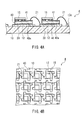
- FIG. 9A is a schematic perspective view of the LED light source of JP 10(1998)-62786 A
- FIG. 9B is a perspective plan view of the same.
- conductor patterns 102 are formed on a base material 101, and a plurality of LED chips 103 are die-bonded to the conductor patterns 102 and connected in series via wires 104.
- each of the wires 104 extends from the LED chip 103 to the conductor pattern 102 in the same direction when viewed perpendicularly to the base material 101. Therefore, shadows of the wires 104 overlap while light emitted from each of the LED chips 103 is condensed by a condenser lens. As a result, luminance nonuniformity is likely to occur on an irradiation plane.
- the document JP 2002 033522 A describes a light-emitting module, in which light-emitting elements are mounted on mount portions and are connected to a conductor pattern via a plurality of wires.
- the wires extend from contact pads to the conductor pattern.
- the light-emitting elements are rotated by 180 degrees with respect to each other around a rotation axis extending perpendicularly to the mounting board.
- Document US 6014202 A describes a light-emitting module arranged to reduce an asymmetric light drop off due to the bonding wires by providing LEDs in pairs, wherein bonding wires to the luminuous surfaces of each pair extend in opposite directions.
- the present invention provides a light-emitting module that can suppress the luminance nonuniformity caused by the shadows of wires, and a mounting board used for the light-emitting module.
- Alight-emitting module of the present invention includes a mounting board with a conductor pattern and a plurality of light-emitting elements mounted on the conductor pattern via wires.
- the extending direction of each of the wires toward the conductor pattern is oriented irregularly when viewed perpendicularly to the mounting board.
- Amounting board of the present invention is used for mounting a plurality of light-emitting elements with a substantially square or rectangular shape by wire bonding.
- the mounting board includes a conductor pattern that includes a plurality of mount portions carrying the light-emitting elements.
- the mount portion When the light-emitting element is mounted on the mount portion and viewed perpendicularly to the mounting board, the mount portion has peripheral portions that are located outside of each side of the light-emitting element.
- Alight-emitting module of the present invention includes a mounting board with a conductor pattern and a plurality of light-emitting elements mounted on the conductor pattern via wires.
- the mounting board includes, e.g., a base material and the conductor pattern formed on the base material.
- the base material is not particularly limited and may be a ceramic material such as Al 2 O 3 or AlN, a semiconductor material such as Si, or a laminated material in which an electric insulating layer is formed on a metal layer.
- As the electric insulating layer e.g., a composite material including 50 to 95 mass% of inorganic filler and 5 to 50 mass% of thermosetting resin composition can be used.
- the material of the wire also is not particularly limited, and a wire made of metal such as a gold wire can be used.
- the wire diameter is preferably 30 ⁇ m or less because the area of a shadow of the wire can be reduced to suppress the luminance nonuniformity In general, the wire diameter is 15 ⁇ m or more.
- the light-emitting element may be, e.g., a red LED chip for emitting red light with a wavelength of 590 to 650 nm, a green LED chip for emitting green light with a wavelength of 500 to 550 nm, or a blue LED chip for emitting blue light with a wavelength of 450 to 500 nm.
- the red LED chip may be made of a AlInGaP material
- the green or blue LED chip may be made of a InGaAlN material.
- the number of the light-emitting elements is not particularly limited and may be determined appropriately in accordance with the luminous energy to be required or the like.
- the light-emitting module of the present invention may include the blue LED chips as the light-emitting elements.
- the light-emitting elements may be covered with a phosphor layer that emits fluorescence by absorption of light emitted from the light-emitting elements.
- the phosphor layer can be formed by producing a paste in which a phosphor that absorbs light emitted from the light-emitting elements and emits fluorescence is dispersed in a silicone resin or the like and applying the paste to the light-emitting elements.
- the phosphor examples include a green light emitting phosphor such as Y 3 (Al, Ga) 5 O 12 : Ce 3+ with a garnet structure or silicate (Ba, Sr) 2 SiO 4 : Eu 2+ , a yellow light emitting phosphor such as SIALON Ca-Al-Si-O-N : Eu 2+ , silicate (Sr, Ca) 2 SiO 4 : Eu 2+ , or (Y, Gd) 3 Al 5 O 12 : Ce 3+ with a garnet structure, and a red light emitting phosphor such as nitridosilicate Sr 2 Si 5 N 8 : Eu 2+ , nitridoaluminosilicate CaAlSiN 3 : Eu 2+ , oxo-nitridoaluminosilicate Sr 2 Si 4 AlON 7 : Eu 2+ , or sulfide CaS : Eu 2+ .
- a green light emitting phosphor such as Y
- the extending direction of each of the wires toward the conductor pattern is oriented irregularly when viewed perpendicularly to the mounting board. This can prevent the shadows of the wires from overlapping, and thus can suppress the luminance nonuniformity
- the definition that "the extending direction is oriented irregularly" indicates that the wires extend irregularly in the light-emitting module as a whole, and some of the wires may extend regularly in a part of the light-emitting module.
- the light-emitting module of the present invention includes a plurality of light-emitting units that are arranged in parallel on the mounting board, and each of the light-emitting units includes the light-emitting elements connected in series via the wires and the conductor pattern
- the adjacent light-emitting units may differ in the extending direction of each of the wires.
- all the wires in the same light-emitting unit may extend in the same direction.
- the wires used for mounting each of the adjacent light-emitting elements may extend in different directions. This can prevent the overlapping of the shadows of the wires more effectively.
- each of the wires may extend from the edge of the light-emitting element to the conductor pattern when viewed perpendicularly to the mounting board. This reduces a region where the wire overlaps the luminous surface of the light-emitting element, so that the area of a shadow of the wire can be reduced to suppress the luminance nonuniformity
- the "edge" may range from one side of the light-emitting element to a position that is 0.4 L inward, and preferably 0.3 L inward from the side, where L represents the length of the side.
- the light-emitting module of the present invention further may include a plurality of sub-mount substrates, on each of which the light-emitting element is mounted.
- the sub-mount substrates may be mounted on the conductor pattern via the wires.
- the mounting board is suitable for the above light-emitting module of the present invention. Therefore, the explanation that overlaps with that of the light-emitting module may be omitted in the following.
- the mounting board of the present invention is used for mounting a plurality of light-emitting elements with a substantially square or rectangular shape by wire bonding.
- the mounting board includes a conductor pattern that includes a plurality of mount portions carrying the light-emitting elements.
- the mount portion When the light-emitting element is mounted on the mount portion and viewed perpendicularly to the mounting board, the mount portion has peripheral portions that are located outside of each side of the light-emitting element. Since the peripheral portions can serve as connection terminals of the wires, the wire is allowed to extend in any direction of the four sides of the light-emitting element. Thus, the mounting board can make it easier to produce the light-emitting module of the present invention.
- the area of each of the peripheral portions is 0.001 to 0.250 mm 2 . With this range, the bonding can be performed easily using the wires without reducing the packaging density of the light-emitting elements.
- FIG. 1A is a plan view of the mounting board of Embodiment 1.
- FIG. 1B is a plan view of a mount portion included in the mounting board of FIG. 1A , on which a LED chip is mounted.
- the mounting board 1 of Embodiment 1 includes a base material 10 and a conductor pattern 11 formed on the base material 10.
- the conductor pattern 11 includes a plurality of mount portions 12, a plurality of external connection terminals 13, and a plurality of lead portions 14 for connecting the mount portion 12 and the external connection terminals 13.
- the mount portion 12 has four peripheral portions 12a.
- the peripheral portions 12a are located outside of each side of the LED chip 15 (see FIG. 1B ).
- the peripheral portions 12a also can serve as connection terminals of wires 21 (see FIG. 2A ). This allows the wire 21 to extend in any direction of the four sides of the LED chip 15.
- the area of each of the peripheral portions 12a is preferably 0.001 to 0.250 mm 2 , and more preferably 0.0025 to 0.225 mm 2 . With this range, the bonding can be performed easily using the wires 21 without reducing the packaging density of the LED chips 15.
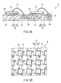
- FIG. 2A is a cross-sectional view of the light-emitting module of Embodiment 2.
- FIG. 2B is a plan view of the light-emitting module of Embodiment 2, as viewed perpendicularly to a mounting board.
- the light-emitting module of Embodiment 2 uses the mounting board 1 of Embodiment 1.
- FIGS. 2A and 2B the same components as those in FIGS. 1A and 1B are denoted by the same reference numerals, and the explanation will not be repeated.
- the light-emitting module 2 of Embodiment 2 includes the mounting board 1 and the LED chips 15.
- the LED chips 15 are die-bonded to each of the mount portions 12 of the mounting board 1 via a conductive adhesive layer 20 made of, e.g., a silver paste.
- the LED chips 15 are connected in series through the wires 21, the mount portions 12, and the conductive adhesive layers 20.
- an electrode (not shown) formed on the upper surface of the LED chip 15 and any of the peripheral portions 12a may be connected by the wire 21.
- the LED chips 15 connected in series constitute LED chip units 22 that become longer in the lateral direction of the drawing, and the LED chip units 22 are arranged in parallel on the base material 10. Moreover, the adjacent LED chip units 22 differ in the extending direction of each of the wires 21 toward the mount portions 12. This can prevent the shadows of the wires 21 from overlapping, and thus can suppress the luminance nonuniformity.
- all the wires 21 in the same LED chip unit 22 extend in the same direction. Such a configuration facilitates the mounting process of the LED chips 15 with the wires 21 during formation of the LED chip unit 22.
- the light-emitting module of an embodiment has been described, but the present invention is not limited thereto.
- all the wires in the same LED chip unit extend in the same direction in the above embodiment, at least one wire may extend in a different direction from the other wires in the same LED chip unit.
- FIG. 3 is a plan view of the light-emitting module of Embodiment 3, as viewed perpendicularly to a mounting board.
- the same components as those in FIGS. 2A and 2B are denoted by the same reference numerals, and the explanation will not be repeated.
- the light-emitting module 3 of Embodiment 3 includes the LED chip units 22 that become longer in the vertical direction of the drawing.
- the individual LED chip units 22 are composed of the LED chips 15 connected in series in the vertical direction of the drawing.
- the other configurations of the light-emitting module 3 are the same as those of the light-emitting module 2.
- the light-emitting module 3 also can have an effect comparable to that of the light-emitting module 2.
- FIG. 4A is a cross-sectional view of the light-emitting module of Embodiment 4.
- FIG. 4B is a plan view of the light-emitting module of Embodiment 4, as viewed perpendicularly to a mounting board.
- the same components as those in FIGS. 2A and 2B are denoted by the same reference numerals, and the explanation will not be repeated.
- the light-emitting module 4 of Embodiment 4 includes sub-mount substrates 40 that are die-bonded to each of the mount portions 12 via the conductive adhesive layer 20 made of, e.g., a silver paste.
- Conductor patterns 40a are formed on the sub-mount substrates 40, and the LED chips 15 are flip-chip mounted on the conductor patterns 40a via bumps 41.
- the adjacent sub-mount substrates 40 are connected electrically through the wires 21, the mount portions 12, and the conductive adhesive layers 20, as shown in FIGS. 4A and 4B .
- the electrical or optical properties of the LED chips 15 can be inspected at the time the LED chips 15 are mounted on the sub-mount substrates 40. Therefore, only non-defective LED chips 15 can be selected and mounted.
- the light-emitting module 4 can suppress the luminance nonuniformity more effectively.
- the other configurations of the light-emitting module 4 are the same as those of the light-emitting module 2.
- FIG. 5A is a cross-sectional view of the light-emitting module of Embodiment 5.
- FIG. 5B is a plan view of the light-emitting module of Embodiment 5, as viewed perpendicularly to a mounting board.
- the same components as those in FIGS. 2A and 2B are denoted by the same reference numerals, and the explanation will not be repeated.
- the light-emitting module 5 of Embodiment 5 includes wiring patterns 50 and via conductors 51 that are provided inside the base material 10.
- the peripheral portions 12a are separated from a central portion 12b on which the LED chip 15 is mounted.
- the adjacent LED chips 15 are connected electrically through the wires 21, the peripheral portions 12a of the mount portions 12, the via conductors 51, the wiring patterns 50, the via conductors 51, the central portions 12b of the mount portions 12, and the conductive adhesive layers 20. Therefore, when the LED chip 15 is mounted by the wire 21, any of the peripheral portions 12a of the mount portion 12 that carries this LED chip 15 can be used as a connection terminal.
- the length of the wires 21 can be made shorter in the light-emitting module 5 (see FIG. 5B ) than in the light-emitting module 2 (see FIG. 2B ), thereby improving the reliability of electric connection with the wires 21.
- the other configurations of the light-emitting module 5 are the same as those of the light-emitting module 2.
- the light-emitting module 5 also can have an effect comparable to that of the light-emitting module 2.
- FIG. 6 is a plan view of the light-emitting module of Embodiment 6, as viewed perpendicularly to a mounting board.
- the same components as those in FIGS. 5A and 5B are denoted by the same reference numerals, and the explanation will not be repeated.
- the light-emitting module 6 of Embodiment 6 includes the LED chips 15 that are connected in series in the vertical direction of the drawing. Moreover, each of the wires 21 extends from the edge of the LED chip 15 to the peripheral portion 12a. Consequently, the length of the wires 21 can be made shorter in the light-emitting module 6 than in the light-emitting module 5 (see FIG. 5B ).
- the light-emitting module 6 reduces a region where the wire 21 overlaps the luminous surface of the LED chip 15, so that the area of a shadow of the wire 21 can be reduced to suppress the luminance nonuniformity.
- the other configurations of the light-emitting module 6 are the same as those of the light-emitting module 5. Thus, the light-emitting module 6 also can have an effect comparable to that of the light-emitting module 5.
- FIG. 7 is a plan view of the light-emitting module of Embodiment 7, as viewed perpendicularly to a mounting board.
- the same components as those in FIGS. 5A and 5B are denoted by the same reference numerals, and the explanation will not be repeated.
- the light-emitting module 7 of Embodiment 7 includes three peripheral portions 12a for each side of the central portion 12b.
- the wires 21 used for mounting each of the adjacent LED chips 15 extend in different directions. This can prevent the overlapping of the shadows of the wires 21 more effectively.
- the other configurations of the light-emitting module 7 are the same as those of the light-emitting module 5.
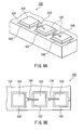
- FIG. 8A is a plan view of a mount portion included in the light-emitting module of Embodiment 8.
- FIG. 8B is a plan view of the mount portion of FIG. 8A , on which a LED chip is mounted.
- FIG. 8C is a plan view of the light-emitting module of Embodiment 8, as viewed perpendicularly to a mounting board.
- the same components as those in FIGS. 5A and 5B are denoted by the same reference numerals, and the explanation will not be repeated.
- the mount portion 12 of the light-emitting module 8 includes a first terminal 12c and a second terminal 12d. Both the first and second terminals 12c, 12d have notches 12e that correspond to predetermined portions of the outer edge of the LED chip 15. By using the notches 12e as positioning marks, the LED chip 15 can be mounted in the center of the mount portion 12, as shown in FIG. 8B . In the mount portion 12 of FIG. 8B , the portions beyond each side of the LED chip 15 can be identified as "peripheral portions".
- a first electrode 15a and a second electrode 15b are formed on the upper surface of the LED chip 15.
- the first electrode 15a is connected electrically to the first terminal 12c via the wire 21, and the second electrode 15b is connected electrically to the second terminal 12d via the wire 21, as shown in FIG. 8C .
- the extending direction of each of the wires 21 is oriented irregularly in the light-emitting module 8. Accordingly, the light-emitting module 8 also can prevent the shadows of the wires 21 from overlapping, and thus can suppress the luminance nonuniformity.
- a light-emitting module of the present invention is suitable for a lighting unit used, e.g., in general lighting applications, lighting for presentation purposes (such as a sign light), or vehicle lighting (particularly a headlight) or a display unit used, e.g., in outdoor large display screens or projectors.
Landscapes
- Engineering & Computer Science (AREA)
- Physics & Mathematics (AREA)
- Microelectronics & Electronic Packaging (AREA)
- Optics & Photonics (AREA)
- General Engineering & Computer Science (AREA)
- Led Device Packages (AREA)
Description
- The present invention relates to a light-emitting module including light-emitting elements, and a mounting board used for the light-emitting module.
- A light-emitting element such as a light emitting diode (referred to as "LED" in the following) or semiconductor laser has been used, e.g., as a light source for a liquid crystal backlight, an indicator, a display, and a read sensor.
- For example,
JP 10(1998)-62786 A FIG. 9A is a schematic perspective view of the LED light source ofJP 10(1998)-62786 A FIG. 9B is a perspective plan view of the same. - In the
LED light source 100 ofFIG. 9A ,conductor patterns 102 are formed on abase material 101, and a plurality ofLED chips 103 are die-bonded to theconductor patterns 102 and connected in series viawires 104. - However, as shown in
FIG. 9B , each of thewires 104 extends from theLED chip 103 to theconductor pattern 102 in the same direction when viewed perpendicularly to thebase material 101. Therefore, shadows of thewires 104 overlap while light emitted from each of theLED chips 103 is condensed by a condenser lens. As a result, luminance nonuniformity is likely to occur on an irradiation plane. - In the Japanese patent application
JP 2002 373 508 A - The document
JP 2002 033522 A - Document
US 6014202 A describes a light-emitting module arranged to reduce an asymmetric light drop off due to the bonding wires by providing LEDs in pairs, wherein bonding wires to the luminuous surfaces of each pair extend in opposite directions. - With the foregoing in mind, the present invention provides a light-emitting module that can suppress the luminance nonuniformity caused by the shadows of wires, and a mounting board used for the light-emitting module.
- Alight-emitting module of the present invention includes a mounting board with a conductor pattern and a plurality of light-emitting elements mounted on the conductor pattern via wires. The extending direction of each of the wires toward the conductor pattern is oriented irregularly when viewed perpendicularly to the mounting board.
- Amounting board of the present invention is used for mounting a plurality of light-emitting elements with a substantially square or rectangular shape by wire bonding. The mounting board includes a conductor pattern that includes a plurality of mount portions carrying the light-emitting elements. When the light-emitting element is mounted on the mount portion and viewed perpendicularly to the mounting board, the mount portion has peripheral portions that are located outside of each side of the light-emitting element.
-
-
FIG. 1A is a plan view of a mounting board of Embodiment 1 of the present invention.FIG. 1B is a plan view of a mount portion included in the mounting board ofFIG. 1A , on which a LED chip is mounted. -
FIG. 2A is a cross-sectional view of a light-emitting module ofEmbodiment 2 of the present invention.FIG. 2B is a plan view of the light-emitting module ofEmbodiment 2, as viewed perpendicularly to a mounting board. -
FIG. 3 is a plan view of a light-emitting module ofEmbodiment 3 of the present invention, as viewed perpendicularly to a mounting board. -
FIG. 4A is a cross-sectional view of a light-emitting module of Embodiment 4 of the present invention.FIG. 4B is a plan view of the light-emitting module of Embodiment 4, as viewed perpendicularly to a mounting board. -
FIG. 5A is a cross-sectional view of a light-emitting module ofEmbodiment 5 of the present invention.FIG. 5B is a plan view of the light-emitting module ofEmbodiment 5, as viewed perpendicularly to a mounting board. -
FIG. 6 is a plan view of a light-emitting module ofEmbodiment 6 of the present invention, as viewed perpendicularly to a mounting board. -
FIG. 7 is a plan view of a light-emitting module of Embodiment 7 of the present invention, as viewed perpendicularly to a mounting board. -
FIG. 8A is a plan view of a mount portion included in a light-emitting module ofEmbodiment 8 of the present invention.FIG. 8B is a plan view of the mount portion ofFIG. 8A , on which a LED chip is mounted.FIG. 8C is a plan view of the light-emitting module ofEmbodiment 8, as viewed perpendicularly to a mounting board. -
FIG. 9A is a schematic perspective view of a conventional LED light source.FIG. 9B is a schematic plan view of the conventional LED light source. - Alight-emitting module of the present invention includes a mounting board with a conductor pattern and a plurality of light-emitting elements mounted on the conductor pattern via wires.
- The mounting board includes, e.g., a base material and the conductor pattern formed on the base material. The base material is not particularly limited and may be a ceramic material such as Al2O3 or AlN, a semiconductor material such as Si, or a laminated material in which an electric insulating layer is formed on a metal layer. As the electric insulating layer, e.g., a composite material including 50 to 95 mass% of inorganic filler and 5 to 50 mass% of thermosetting resin composition can be used. The material of the wire also is not particularly limited, and a wire made of metal such as a gold wire can be used. The wire diameter is preferably 30 µm or less because the area of a shadow of the wire can be reduced to suppress the luminance nonuniformity In general, the wire diameter is 15 µm or more.
- The light-emitting element may be, e.g., a red LED chip for emitting red light with a wavelength of 590 to 650 nm, a green LED chip for emitting green light with a wavelength of 500 to 550 nm, or a blue LED chip for emitting blue light with a wavelength of 450 to 500 nm. The red LED chip may be made of a AlInGaP material, and the green or blue LED chip may be made of a InGaAlN material. The number of the light-emitting elements is not particularly limited and may be determined appropriately in accordance with the luminous energy to be required or the like.
- When the light-emitting module of the present invention is used as a white light source, it may include the blue LED chips as the light-emitting elements. Moreover, the light-emitting elements may be covered with a phosphor layer that emits fluorescence by absorption of light emitted from the light-emitting elements. For example, the phosphor layer can be formed by producing a paste in which a phosphor that absorbs light emitted from the light-emitting elements and emits fluorescence is dispersed in a silicone resin or the like and applying the paste to the light-emitting elements. Examples of the phosphor include a green light emitting phosphor such as Y3(Al, Ga)5O12 : Ce3+ with a garnet structure or silicate (Ba, Sr)2SiO4 : Eu2+, a yellow light emitting phosphor such as SIALON Ca-Al-Si-O-N : Eu2+, silicate (Sr, Ca)2SiO4 : Eu2+, or (Y, Gd)3Al5O12 : Ce3+ with a garnet structure, and a red light emitting phosphor such as nitridosilicate Sr2Si5N8 : Eu2+, nitridoaluminosilicate CaAlSiN3 : Eu2+, oxo-nitridoaluminosilicate Sr2Si4AlON7 : Eu2+, or sulfide CaS : Eu2+.
- In the light-emitting module of the present invention, the extending direction of each of the wires toward the conductor pattern is oriented irregularly when viewed perpendicularly to the mounting board. This can prevent the shadows of the wires from overlapping, and thus can suppress the luminance nonuniformity In the context of the present invention, the definition that "the extending direction is oriented irregularly" indicates that the wires extend irregularly in the light-emitting module as a whole, and some of the wires may extend regularly in a part of the light-emitting module. For example, when the light-emitting module of the present invention includes a plurality of light-emitting units that are arranged in parallel on the mounting board, and each of the light-emitting units includes the light-emitting elements connected in series via the wires and the conductor pattern, the adjacent light-emitting units may differ in the extending direction of each of the wires. In this case, all the wires in the same light-emitting unit may extend in the same direction. Such a configuration facilitates the mounting process of the light-emitting elements with the wires during formation of the light-emitting unit.
- In the light-emitting module of the present invention, the wires used for mounting each of the adjacent light-emitting elements may extend in different directions. This can prevent the overlapping of the shadows of the wires more effectively.
- In the light-emitting module of the present invention, each of the wires may extend from the edge of the light-emitting element to the conductor pattern when viewed perpendicularly to the mounting board. This reduces a region where the wire overlaps the luminous surface of the light-emitting element, so that the area of a shadow of the wire can be reduced to suppress the luminance nonuniformity In this case, the "edge" may range from one side of the light-emitting element to a position that is 0.4 L inward, and preferably 0.3 L inward from the side, where L represents the length of the side.
- The light-emitting module of the present invention further may include a plurality of sub-mount substrates, on each of which the light-emitting element is mounted. The sub-mount substrates may be mounted on the conductor pattern via the wires. With this configuration, the electrical or optical properties of the light-emitting elements can be inspected at the time the light-emitting elements are mounted on the sub-mount substrates. Therefore, only non-defective light-emitting elements can be selected and mounted. Thus, it is possible to avoid waste in the manufacturing process of the light-emitting module and improve yields. The material of the sub-mount substrate is not particularly limited, and the same materials as those for the mounting board can be used.
- Next, a mounting board of the present invention will be described below. The mounting board is suitable for the above light-emitting module of the present invention. Therefore, the explanation that overlaps with that of the light-emitting module may be omitted in the following.
- The mounting board of the present invention is used for mounting a plurality of light-emitting elements with a substantially square or rectangular shape by wire bonding. The mounting board includes a conductor pattern that includes a plurality of mount portions carrying the light-emitting elements. When the light-emitting element is mounted on the mount portion and viewed perpendicularly to the mounting board, the mount portion has peripheral portions that are located outside of each side of the light-emitting element. Since the peripheral portions can serve as connection terminals of the wires, the wire is allowed to extend in any direction of the four sides of the light-emitting element. Thus, the mounting board can make it easier to produce the light-emitting module of the present invention.
- In the mounting board of the present invention, it is preferable that the area of each of the peripheral portions is 0.001 to 0.250 mm2. With this range, the bonding can be performed easily using the wires without reducing the packaging density of the light-emitting elements.
- Hereinafter, embodiments of the present invention will be described in detail.
- A mounting board of
Embodiment 1 of the present invention will be described by referring to the drawings.FIG. 1A is a plan view of the mounting board ofEmbodiment 1.FIG. 1B is a plan view of a mount portion included in the mounting board ofFIG. 1A , on which a LED chip is mounted. - As shown in
FIG. 1A , the mountingboard 1 ofEmbodiment 1 includes abase material 10 and aconductor pattern 11 formed on thebase material 10. Theconductor pattern 11 includes a plurality ofmount portions 12, a plurality ofexternal connection terminals 13, and a plurality oflead portions 14 for connecting themount portion 12 and theexternal connection terminals 13. - As shown in
FIG. 1B , themount portion 12 has fourperipheral portions 12a. When a substantiallysquare LED chip 15 is mounted on themount portion 12 and viewed perpendicularly to the mountingboard 1, theperipheral portions 12a are located outside of each side of the LED chip 15 (seeFIG. 1B ). Thus, theperipheral portions 12a also can serve as connection terminals of wires 21 (seeFIG. 2A ). This allows thewire 21 to extend in any direction of the four sides of theLED chip 15. The area of each of theperipheral portions 12a is preferably 0.001 to 0.250 mm2, and more preferably 0.0025 to 0.225 mm2. With this range, the bonding can be performed easily using thewires 21 without reducing the packaging density of the LED chips 15. - A light-emitting module of
Embodiment 2 of the present invention will be described by referring to the drawings.FIG. 2A is a cross-sectional view of the light-emitting module ofEmbodiment 2.FIG. 2B is a plan view of the light-emitting module ofEmbodiment 2, as viewed perpendicularly to a mounting board. The light-emitting module ofEmbodiment 2 uses the mountingboard 1 ofEmbodiment 1. InFIGS. 2A and 2B , the same components as those inFIGS. 1A and 1B are denoted by the same reference numerals, and the explanation will not be repeated. - As shown in
FIG. 2A , the light-emittingmodule 2 ofEmbodiment 2 includes the mountingboard 1 and the LED chips 15. The LED chips 15 are die-bonded to each of themount portions 12 of the mountingboard 1 via a conductiveadhesive layer 20 made of, e.g., a silver paste. The LED chips 15 are connected in series through thewires 21, themount portions 12, and the conductive adhesive layers 20. For example, an electrode (not shown) formed on the upper surface of theLED chip 15 and any of theperipheral portions 12a may be connected by thewire 21. - As shown in
FIG. 2B , the LED chips 15 connected in series constituteLED chip units 22 that become longer in the lateral direction of the drawing, and theLED chip units 22 are arranged in parallel on thebase material 10. Moreover, the adjacentLED chip units 22 differ in the extending direction of each of thewires 21 toward themount portions 12. This can prevent the shadows of thewires 21 from overlapping, and thus can suppress the luminance nonuniformity. - In the light-emitting
module 2, all thewires 21 in the sameLED chip unit 22 extend in the same direction. Such a configuration facilitates the mounting process of the LED chips 15 with thewires 21 during formation of theLED chip unit 22. - The light-emitting module of an embodiment has been described, but the present invention is not limited thereto. For example, although all the wires in the same LED chip unit extend in the same direction in the above embodiment, at least one wire may extend in a different direction from the other wires in the same LED chip unit.
- A light-emitting module of
Embodiment 3 of the present invention will be described by referring to the drawings.FIG. 3 is a plan view of the light-emitting module ofEmbodiment 3, as viewed perpendicularly to a mounting board. InFIG. 3 , the same components as those inFIGS. 2A and 2B are denoted by the same reference numerals, and the explanation will not be repeated. - As shown in
FIG. 3 , the light-emittingmodule 3 ofEmbodiment 3 includes theLED chip units 22 that become longer in the vertical direction of the drawing. In other words, the individualLED chip units 22 are composed of the LED chips 15 connected in series in the vertical direction of the drawing. The other configurations of the light-emittingmodule 3 are the same as those of the light-emittingmodule 2. Thus, the light-emittingmodule 3 also can have an effect comparable to that of the light-emittingmodule 2. - Alight-emitting module of Embodiment 4 of the present invention will be described by referring to the drawings.
FIG. 4A is a cross-sectional view of the light-emitting module of Embodiment 4.FIG. 4B is a plan view of the light-emitting module of Embodiment 4, as viewed perpendicularly to a mounting board. InFIGS. 4A and 4B , the same components as those inFIGS. 2A and 2B are denoted by the same reference numerals, and the explanation will not be repeated. - As shown in
FIG. 4A , the light-emitting module 4 of Embodiment 4 includessub-mount substrates 40 that are die-bonded to each of themount portions 12 via the conductiveadhesive layer 20 made of, e.g., a silver paste.Conductor patterns 40a are formed on thesub-mount substrates 40, and the LED chips 15 are flip-chip mounted on theconductor patterns 40a via bumps 41. The adjacentsub-mount substrates 40 are connected electrically through thewires 21, themount portions 12, and the conductiveadhesive layers 20, as shown inFIGS. 4A and 4B . In the light-emitting module 4, the electrical or optical properties of the LED chips 15 can be inspected at the time the LED chips 15 are mounted on thesub-mount substrates 40. Therefore, only non-defective LED chips 15 can be selected and mounted. - As shown in
FIG. 4B , nowire 21 extends across the luminous surface of theLED chip 15. Thus, the light-emitting module 4 can suppress the luminance nonuniformity more effectively. The other configurations of the light-emitting module 4 are the same as those of the light-emittingmodule 2. - A light-emitting module of
Embodiment 5 of the present invention will be described by referring to the drawings.FIG. 5A is a cross-sectional view of the light-emitting module ofEmbodiment 5.FIG. 5B is a plan view of the light-emitting module ofEmbodiment 5, as viewed perpendicularly to a mounting board. InFIGS. 5A and 5B , the same components as those inFIGS. 2A and 2B are denoted by the same reference numerals, and the explanation will not be repeated. - As shown in
FIG. 5A , the light-emittingmodule 5 ofEmbodiment 5 includeswiring patterns 50 and viaconductors 51 that are provided inside thebase material 10. In each of themount portions 12 of the light-emittingmodule 5, theperipheral portions 12a are separated from acentral portion 12b on which theLED chip 15 is mounted. Theadjacent LED chips 15 are connected electrically through thewires 21, theperipheral portions 12a of themount portions 12, the viaconductors 51, thewiring patterns 50, the viaconductors 51, thecentral portions 12b of themount portions 12, and the conductive adhesive layers 20. Therefore, when theLED chip 15 is mounted by thewire 21, any of theperipheral portions 12a of themount portion 12 that carries thisLED chip 15 can be used as a connection terminal. Consequently, the length of thewires 21 can be made shorter in the light-emitting module 5 (seeFIG. 5B ) than in the light-emitting module 2 (seeFIG. 2B ), thereby improving the reliability of electric connection with thewires 21. The other configurations of the light-emittingmodule 5 are the same as those of the light-emittingmodule 2. Thus, the light-emittingmodule 5 also can have an effect comparable to that of the light-emittingmodule 2. - Alight-emitting module of
Embodiment 6 of the present invention will be described by referring to the drawings.FIG. 6 is a plan view of the light-emitting module ofEmbodiment 6, as viewed perpendicularly to a mounting board. InFIG. 6 , the same components as those inFIGS. 5A and 5B are denoted by the same reference numerals, and the explanation will not be repeated. - As shown in
FIG. 6 , the light-emittingmodule 6 ofEmbodiment 6 includes the LED chips 15 that are connected in series in the vertical direction of the drawing. Moreover, each of thewires 21 extends from the edge of theLED chip 15 to theperipheral portion 12a. Consequently, the length of thewires 21 can be made shorter in the light-emittingmodule 6 than in the light-emitting module 5 (seeFIG. 5B ). The light-emittingmodule 6 reduces a region where thewire 21 overlaps the luminous surface of theLED chip 15, so that the area of a shadow of thewire 21 can be reduced to suppress the luminance nonuniformity. The other configurations of the light-emittingmodule 6 are the same as those of the light-emittingmodule 5. Thus, the light-emittingmodule 6 also can have an effect comparable to that of the light-emittingmodule 5. - A light-emitting module of Embodiment 7 of the present invention will be described by referring to the drawings.
FIG. 7 is a plan view of the light-emitting module of Embodiment 7, as viewed perpendicularly to a mounting board. InFIG. 7 , the same components as those inFIGS. 5A and 5B are denoted by the same reference numerals, and the explanation will not be repeated. - As shown in
FIG. 7 , the light-emitting module 7 of Embodiment 7 includes threeperipheral portions 12a for each side of thecentral portion 12b. In the light-emitting module 7, thewires 21 used for mounting each of theadjacent LED chips 15 extend in different directions. This can prevent the overlapping of the shadows of thewires 21 more effectively. The other configurations of the light-emitting module 7 are the same as those of the light-emittingmodule 5. - A light-emitting module of
Embodiment 8 of the present invention will be described by referring to the drawings.FIG. 8A is a plan view of a mount portion included in the light-emitting module ofEmbodiment 8.FIG. 8B is a plan view of the mount portion ofFIG. 8A , on which a LED chip is mounted.FIG. 8C is a plan view of the light-emitting module ofEmbodiment 8, as viewed perpendicularly to a mounting board. InFIGS. 8A to 8C , the same components as those inFIGS. 5A and 5B are denoted by the same reference numerals, and the explanation will not be repeated. - As shown in
FIG. 8A , themount portion 12 of the light-emitting module 8 (seeFIG. 8C ) includes afirst terminal 12c and asecond terminal 12d. Both the first andsecond terminals notches 12e that correspond to predetermined portions of the outer edge of theLED chip 15. By using thenotches 12e as positioning marks, theLED chip 15 can be mounted in the center of themount portion 12, as shown inFIG. 8B . In themount portion 12 ofFIG. 8B , the portions beyond each side of theLED chip 15 can be identified as "peripheral portions". - As shown in
FIGS. 8B and 8C , afirst electrode 15a and asecond electrode 15b are formed on the upper surface of theLED chip 15. Thefirst electrode 15a is connected electrically to thefirst terminal 12c via thewire 21, and thesecond electrode 15b is connected electrically to thesecond terminal 12d via thewire 21, as shown inFIG. 8C . Like the light-emittingmodules 2 to 7, the extending direction of each of thewires 21 is oriented irregularly in the light-emittingmodule 8. Accordingly, the light-emittingmodule 8 also can prevent the shadows of thewires 21 from overlapping, and thus can suppress the luminance nonuniformity. - A light-emitting module of the present invention is suitable for a lighting unit used, e.g., in general lighting applications, lighting for presentation purposes (such as a sign light), or vehicle lighting (particularly a headlight) or a display unit used, e.g., in outdoor large display screens or projectors.
Claims (7)
- A light-emitting module comprising:a mounting board (1) with a conductor pattern (11) including a plurality of mount portions (12); anda plurality of light-emitting units (22), each unit comprising a plurality of light-emitting elements (15) connected in series, the plurality of light-emitting elements (15) being mounted on mount portions (12) of the conductor pattern (11) such that luminous surfaces of the light-emitting elements face away from the mounting board (1) and being connected to the conductor pattern (11) via a plurality of wires (21), with the wires (21) overlapping said luminous surfaces of the light-emitting elements (15);wherein the wires (21) extending from said luminous surfaces of the light-emitting elements (15) toward the conductor pattern (11) do not all extend in the same direction when viewed perpendicularly to the mounting board (1);characterized in thatthe light-emitting units (22) are spatially arranged in parallel on the mounting board (1); andadjacent ones of the light-emitting units (22) differ in the extending direction of each of the wires (21).
- The light-emitting module according to claim 1, wherein all the wires (21) in the same light-emitting unit (22) extend in the same direction.
- The light-emitting module according to claim 1, wherein the wires (21) connecting each of the adjacent light-emitting elements (15) to the conductor pattern extend in different directions.
- The light-emitting module according to claim 1, wherein each of the wires (21) extends from an edge of the light-emitting element (15) to the conductor pattern (11) when viewed perpendicularly to the mounting board (1).
- The light-emitting module according to any one of claims 1 to 5, wherein the wires (21) have a diameter of 30 µm or less.
- A mounting board (1) for mounting a plurality of light-emitting elements (15) with a substantially square or rectangular shape by wire bonding, comprising:a conductor pattern (11) that comprises a plurality of substantially square or rectangular shaped mount portions (12) for carrying the light-emitting elements (15),characterized in thatwhen viewed perpendicularly to the mounting board (1), each mount portion (12) has peripheral conductive pads (12a) that are located outside of each side of the mount portion for the light-emitting element (15),each of the peripheral conductive pads (12a) is separated from or integrated with the corresponding mount portion (12),in each pair of opposing sides of each mount portion for the light-emitting elements (15), the peripheral conductive pads (12a) located outside of each of the pair of opposing sides of the mount portion for the light-emitting element (15) are arranged so as not to face each other with the mount portion (12) there between,such that, when the mounting board is provided with light-emitting elements, wires (21) extending from luminous surfaces of the light-emitting elements (15) toward peripheral conductive pads of the conductor pattern (11) can be provided not all extending in the same direction when viewed perpendicularly to the mounting board (1).
- The mounting board (1) according to claim 6, wherein an area of each of the peripheral portions (12a) is 0.001 mm2 to 0.250 mm2.
Applications Claiming Priority (2)
| Application Number | Priority Date | Filing Date | Title |
|---|---|---|---|
| JP2005207352 | 2005-07-15 | ||
| PCT/JP2006/314118 WO2007010879A2 (en) | 2005-07-15 | 2006-07-10 | Light-emitting module and mounting board used therefor |
Publications (2)
| Publication Number | Publication Date |
|---|---|
| EP1908124A2 EP1908124A2 (en) | 2008-04-09 |
| EP1908124B1 true EP1908124B1 (en) | 2015-06-24 |
Family
ID=37669245
Family Applications (1)
| Application Number | Title | Priority Date | Filing Date |
|---|---|---|---|
| EP06781143.0A Active EP1908124B1 (en) | 2005-07-15 | 2006-07-10 | Light-emitting module and corresponding circuit board |
Country Status (5)
| Country | Link |
|---|---|
| US (1) | US7902568B2 (en) |
| EP (1) | EP1908124B1 (en) |
| JP (1) | JP5065057B2 (en) |
| TW (1) | TWI395342B (en) |
| WO (1) | WO2007010879A2 (en) |
Families Citing this family (24)
| Publication number | Priority date | Publication date | Assignee | Title |
|---|---|---|---|---|
| US7940673B2 (en) * | 2007-06-06 | 2011-05-10 | Veedims, Llc | System for integrating a plurality of modules using a power/data backbone network |
| US8303337B2 (en) | 2007-06-06 | 2012-11-06 | Veedims, Llc | Hybrid cable for conveying data and power |
| US8421093B2 (en) * | 2007-07-13 | 2013-04-16 | Rohm Co., Ltd. | LED module and LED dot matrix display |
| US7856158B2 (en) | 2008-03-07 | 2010-12-21 | Ballard Claudio R | Virtual electronic switch system |
| US7963559B2 (en) * | 2008-03-07 | 2011-06-21 | Claudio R. Ballard | Roll bar with integrated lighting |
| AT506709B1 (en) * | 2008-05-30 | 2009-11-15 | Kuster Martin | LAMPS |
| US8058669B2 (en) * | 2008-08-28 | 2011-11-15 | Taiwan Semiconductor Manufacturing Company, Ltd. | Light-emitting diode integration scheme |
| FR2943799B1 (en) * | 2009-03-31 | 2011-09-02 | Valeo Vision Sas | "LENS FOR LIGHTING MODULE FOR MOTOR VEHICLE". |
| JP5407993B2 (en) * | 2010-03-31 | 2014-02-05 | 豊田合成株式会社 | Vehicle headlamp |
| MX2013005202A (en) * | 2010-03-30 | 2013-11-20 | Changchn Inst Of Applied Chemistry Chinese Academy Of Sciences | ALTERNATE CURRENT DEVICE OF WHITE LED. |
| JP5528900B2 (en) * | 2010-04-30 | 2014-06-25 | ローム株式会社 | Light emitting element module |
| TWD141522S1 (en) * | 2010-06-10 | 2011-07-11 | 晶元光電股份有限公司 | Light emitting diode array |
| JP5283195B2 (en) * | 2010-09-07 | 2013-09-04 | シーシーエス株式会社 | LED wiring board and light irradiation device |
| US8696159B2 (en) | 2010-09-20 | 2014-04-15 | Cree, Inc. | Multi-chip LED devices |
| WO2012057038A1 (en) * | 2010-10-26 | 2012-05-03 | 東芝ライテック株式会社 | Light-emitting module and lighting equipment |
| JP5899476B2 (en) * | 2011-06-22 | 2016-04-06 | パナソニックIpマネジメント株式会社 | LIGHT EMITTING DEVICE AND LIGHTING DEVICE USING THE SAME |
| US8976541B2 (en) | 2011-08-31 | 2015-03-10 | Potens Ip Holdings Llc | Electrical power and data distribution apparatus |
| RU2636055C2 (en) * | 2012-04-19 | 2017-11-20 | Филипс Лайтинг Холдинг Б.В. | Led lattice device and method of manufacturing led lattice device |
| JP5999341B2 (en) * | 2012-10-05 | 2016-09-28 | 東芝ライテック株式会社 | Light emitting device and lighting device |
| JP2016096322A (en) * | 2014-11-07 | 2016-05-26 | 日亜化学工業株式会社 | Light emitting device |
| US9589940B2 (en) * | 2014-11-07 | 2017-03-07 | Nichia Corporation | Light emitting device |
| USD768584S1 (en) * | 2014-11-13 | 2016-10-11 | Mitsubishi Electric Corporation | Light source module |
| JP6842246B2 (en) * | 2016-05-26 | 2021-03-17 | ローム株式会社 | LED module |
| CN114556558A (en) * | 2019-07-23 | 2022-05-27 | 亮锐有限责任公司 | Semiconductor light emitting device |
Citations (2)
| Publication number | Priority date | Publication date | Assignee | Title |
|---|---|---|---|---|
| US6014202A (en) * | 1997-09-16 | 2000-01-11 | Polaroid Corporation | Optical system for transmitting a graphical image |
| JP2002033522A (en) * | 2000-07-14 | 2002-01-31 | Mitsubishi Cable Ind Ltd | Circuit board for surface emitting element module |
Family Cites Families (10)
| Publication number | Priority date | Publication date | Assignee | Title |
|---|---|---|---|---|
| JPS636759Y2 (en) * | 1980-08-25 | 1988-02-26 | ||
| JP3059828B2 (en) * | 1992-06-26 | 2000-07-04 | 三洋電機株式会社 | Light emitting diode display |
| FR2707222B1 (en) | 1993-07-07 | 1995-09-29 | Valeo Vision | Improved signaling light with light-emitting diodes. |
| JPH1062786A (en) * | 1996-08-22 | 1998-03-06 | Omron Corp | Light guide device, liquid crystal display device and electronic device |
| JP3399440B2 (en) * | 1999-04-26 | 2003-04-21 | 松下電器産業株式会社 | Composite light emitting element, light emitting device and method of manufacturing the same |
| BR0113923A (en) | 2000-10-10 | 2004-01-13 | Gye-Seon Lee | Led lamp for traffic signal. |
| JP2002373508A (en) | 2001-06-12 | 2002-12-26 | Koshin Denki Kk | Light emitting diode lamp |
| KR100506740B1 (en) * | 2003-12-23 | 2005-08-08 | 삼성전기주식회사 | Nitride semiconductor light emitting device and method of manufacturing the same |
| TWM272232U (en) * | 2005-02-04 | 2005-08-01 | Ya-Huei Ke | Packaging structure of diode |
| TWM281296U (en) * | 2005-06-20 | 2005-11-21 | Shr-Ling Li | Parallel LED module |
-
2006
- 2006-07-10 JP JP2007558363A patent/JP5065057B2/en active Active
- 2006-07-10 US US11/993,729 patent/US7902568B2/en active Active
- 2006-07-10 EP EP06781143.0A patent/EP1908124B1/en active Active
- 2006-07-10 WO PCT/JP2006/314118 patent/WO2007010879A2/en not_active Ceased
- 2006-07-12 TW TW095125421A patent/TWI395342B/en active
Patent Citations (2)
| Publication number | Priority date | Publication date | Assignee | Title |
|---|---|---|---|---|
| US6014202A (en) * | 1997-09-16 | 2000-01-11 | Polaroid Corporation | Optical system for transmitting a graphical image |
| JP2002033522A (en) * | 2000-07-14 | 2002-01-31 | Mitsubishi Cable Ind Ltd | Circuit board for surface emitting element module |
Also Published As
| Publication number | Publication date |
|---|---|
| WO2007010879A2 (en) | 2007-01-25 |
| US20100079997A1 (en) | 2010-04-01 |
| WO2007010879A3 (en) | 2007-06-28 |
| JP5065057B2 (en) | 2012-10-31 |
| JP2009501431A (en) | 2009-01-15 |
| EP1908124A2 (en) | 2008-04-09 |
| US7902568B2 (en) | 2011-03-08 |
| TWI395342B (en) | 2013-05-01 |
| TW200729545A (en) | 2007-08-01 |
Similar Documents
| Publication | Publication Date | Title |
|---|---|---|
| EP1908124B1 (en) | Light-emitting module and corresponding circuit board | |
| US10655801B2 (en) | Light emitting device and vehicular lamp comprising same | |
| US10141491B2 (en) | Method of manufacturing light emitting device | |
| TWI610465B (en) | Light-emitting diode assembly and manufacturing method | |
| CN102237483B (en) | Light-emitting device | |
| CN100576535C (en) | Light emitting device and lighting device using the light emitting device | |
| JP4753904B2 (en) | Light emitting device | |
| EP2669946B1 (en) | Illumination device | |
| JP5118110B2 (en) | Light emitting device | |
| WO2013168802A1 (en) | Led module | |
| US8138517B2 (en) | Light-emitting diode package | |
| US10490721B2 (en) | Light-emitting device and illuminating apparatus | |
| JP5730711B2 (en) | Light emitting device | |
| JP2007294621A (en) | LED lighting device | |
| KR100645657B1 (en) | White light emitting diode module with flip chip printed circuit board and flip chip printed circuit board | |
| JP4753419B2 (en) | Light emitting module | |
| JP5829316B2 (en) | Light emitting device and manufacturing method thereof | |
| TWI713236B (en) | Light-emitting diode assembly and manufacturing method thereof | |
| KR102142718B1 (en) | Light emitting device and light apparatus having thereof | |
| JP6242437B2 (en) | Light emitting device | |
| JP2007142051A (en) | Light emitting module | |
| JP6030193B2 (en) | Light emitting device substrate | |
| JP5980860B2 (en) | LED lamp | |
| CN120283463A (en) | LED luminous element |
Legal Events
| Date | Code | Title | Description |
|---|---|---|---|
| PUAI | Public reference made under article 153(3) epc to a published international application that has entered the european phase |
Free format text: ORIGINAL CODE: 0009012 |
|
| 17P | Request for examination filed |
Effective date: 20080215 |
|
| AK | Designated contracting states |
Kind code of ref document: A2 Designated state(s): AT BE BG CH CY CZ DE DK EE ES FI FR GB GR HU IE IS IT LI LT LU LV MC NL PL PT RO SE SI SK TR |
|
| RAP1 | Party data changed (applicant data changed or rights of an application transferred) |
Owner name: PANASONIC CORPORATION |
|
| 17Q | First examination report despatched |
Effective date: 20081117 |
|
| DAX | Request for extension of the european patent (deleted) | ||
| REG | Reference to a national code |
Ref country code: DE Ref legal event code: R079 Ref document number: 602006045781 Country of ref document: DE Free format text: PREVIOUS MAIN CLASS: H01L0033000000 Ipc: F21K0099000000 |
|
| RIC1 | Information provided on ipc code assigned before grant |
Ipc: F21K 99/00 20100101AFI20140909BHEP Ipc: H01L 25/075 20060101ALI20140909BHEP Ipc: H01L 33/62 20100101ALI20140909BHEP |
|
| GRAP | Despatch of communication of intention to grant a patent |
Free format text: ORIGINAL CODE: EPIDOSNIGR1 |
|
| INTG | Intention to grant announced |
Effective date: 20150109 |
|
| RIN1 | Information on inventor provided before grant (corrected) |
Inventor name: SHIDA, SATOSHI Inventor name: MORIKAWA, MAKOTO Inventor name: UENO, YASUHARU Inventor name: NISHIMOTO, KEIJI Inventor name: NAITO, HIROYUKI Inventor name: UEMOTO, TAKAARI |
|
| RAP1 | Party data changed (applicant data changed or rights of an application transferred) |
Owner name: PANASONIC INTELLECTUAL PROPERTY MANAGEMENT CO., LT |
|
| GRAS | Grant fee paid |
Free format text: ORIGINAL CODE: EPIDOSNIGR3 |
|
| GRAA | (expected) grant |
Free format text: ORIGINAL CODE: 0009210 |
|
| AK | Designated contracting states |
Kind code of ref document: B1 Designated state(s): AT BE BG CH CY CZ DE DK EE ES FI FR GB GR HU IE IS IT LI LT LU LV MC NL PL PT RO SE SI SK TR |
|
| REG | Reference to a national code |
Ref country code: GB Ref legal event code: FG4D |
|
| REG | Reference to a national code |
Ref country code: CH Ref legal event code: EP |
|
| REG | Reference to a national code |
Ref country code: AT Ref legal event code: REF Ref document number: 733067 Country of ref document: AT Kind code of ref document: T Effective date: 20150715 |
|
| REG | Reference to a national code |
Ref country code: IE Ref legal event code: FG4D |
|
| REG | Reference to a national code |
Ref country code: DE Ref legal event code: R096 Ref document number: 602006045781 Country of ref document: DE |
|
| PG25 | Lapsed in a contracting state [announced via postgrant information from national office to epo] |
Ref country code: FI Free format text: LAPSE BECAUSE OF FAILURE TO SUBMIT A TRANSLATION OF THE DESCRIPTION OR TO PAY THE FEE WITHIN THE PRESCRIBED TIME-LIMIT Effective date: 20150624 Ref country code: LT Free format text: LAPSE BECAUSE OF FAILURE TO SUBMIT A TRANSLATION OF THE DESCRIPTION OR TO PAY THE FEE WITHIN THE PRESCRIBED TIME-LIMIT Effective date: 20150624 |
|
| REG | Reference to a national code |
Ref country code: AT Ref legal event code: MK05 Ref document number: 733067 Country of ref document: AT Kind code of ref document: T Effective date: 20150624 |
|
| REG | Reference to a national code |
Ref country code: LT Ref legal event code: MG4D |
|
| PG25 | Lapsed in a contracting state [announced via postgrant information from national office to epo] |
Ref country code: LV Free format text: LAPSE BECAUSE OF FAILURE TO SUBMIT A TRANSLATION OF THE DESCRIPTION OR TO PAY THE FEE WITHIN THE PRESCRIBED TIME-LIMIT Effective date: 20150624 Ref country code: GR Free format text: LAPSE BECAUSE OF FAILURE TO SUBMIT A TRANSLATION OF THE DESCRIPTION OR TO PAY THE FEE WITHIN THE PRESCRIBED TIME-LIMIT Effective date: 20150925 Ref country code: BG Free format text: LAPSE BECAUSE OF FAILURE TO SUBMIT A TRANSLATION OF THE DESCRIPTION OR TO PAY THE FEE WITHIN THE PRESCRIBED TIME-LIMIT Effective date: 20150924 |
|
| REG | Reference to a national code |
Ref country code: NL Ref legal event code: MP Effective date: 20150624 |
|
| PG25 | Lapsed in a contracting state [announced via postgrant information from national office to epo] |
Ref country code: EE Free format text: LAPSE BECAUSE OF FAILURE TO SUBMIT A TRANSLATION OF THE DESCRIPTION OR TO PAY THE FEE WITHIN THE PRESCRIBED TIME-LIMIT Effective date: 20150624 |
|
| PG25 | Lapsed in a contracting state [announced via postgrant information from national office to epo] |
Ref country code: PL Free format text: LAPSE BECAUSE OF FAILURE TO SUBMIT A TRANSLATION OF THE DESCRIPTION OR TO PAY THE FEE WITHIN THE PRESCRIBED TIME-LIMIT Effective date: 20150624 Ref country code: RO Free format text: LAPSE BECAUSE OF NON-PAYMENT OF DUE FEES Effective date: 20150624 Ref country code: IS Free format text: LAPSE BECAUSE OF FAILURE TO SUBMIT A TRANSLATION OF THE DESCRIPTION OR TO PAY THE FEE WITHIN THE PRESCRIBED TIME-LIMIT Effective date: 20151024 Ref country code: PT Free format text: LAPSE BECAUSE OF FAILURE TO SUBMIT A TRANSLATION OF THE DESCRIPTION OR TO PAY THE FEE WITHIN THE PRESCRIBED TIME-LIMIT Effective date: 20151026 Ref country code: SK Free format text: LAPSE BECAUSE OF FAILURE TO SUBMIT A TRANSLATION OF THE DESCRIPTION OR TO PAY THE FEE WITHIN THE PRESCRIBED TIME-LIMIT Effective date: 20150624 Ref country code: ES Free format text: LAPSE BECAUSE OF FAILURE TO SUBMIT A TRANSLATION OF THE DESCRIPTION OR TO PAY THE FEE WITHIN THE PRESCRIBED TIME-LIMIT Effective date: 20150624 Ref country code: AT Free format text: LAPSE BECAUSE OF FAILURE TO SUBMIT A TRANSLATION OF THE DESCRIPTION OR TO PAY THE FEE WITHIN THE PRESCRIBED TIME-LIMIT Effective date: 20150624 Ref country code: CZ Free format text: LAPSE BECAUSE OF FAILURE TO SUBMIT A TRANSLATION OF THE DESCRIPTION OR TO PAY THE FEE WITHIN THE PRESCRIBED TIME-LIMIT Effective date: 20150624 |
|
| REG | Reference to a national code |
Ref country code: CH Ref legal event code: PL |
|
| REG | Reference to a national code |
Ref country code: DE Ref legal event code: R097 Ref document number: 602006045781 Country of ref document: DE |
|
| PG25 | Lapsed in a contracting state [announced via postgrant information from national office to epo] |
Ref country code: MC Free format text: LAPSE BECAUSE OF FAILURE TO SUBMIT A TRANSLATION OF THE DESCRIPTION OR TO PAY THE FEE WITHIN THE PRESCRIBED TIME-LIMIT Effective date: 20150624 |
|
| REG | Reference to a national code |
Ref country code: IE Ref legal event code: MM4A |
|
| PG25 | Lapsed in a contracting state [announced via postgrant information from national office to epo] |
Ref country code: CH Free format text: LAPSE BECAUSE OF NON-PAYMENT OF DUE FEES Effective date: 20150731 Ref country code: LI Free format text: LAPSE BECAUSE OF NON-PAYMENT OF DUE FEES Effective date: 20150731 Ref country code: IT Free format text: LAPSE BECAUSE OF FAILURE TO SUBMIT A TRANSLATION OF THE DESCRIPTION OR TO PAY THE FEE WITHIN THE PRESCRIBED TIME-LIMIT Effective date: 20150624 Ref country code: DK Free format text: LAPSE BECAUSE OF FAILURE TO SUBMIT A TRANSLATION OF THE DESCRIPTION OR TO PAY THE FEE WITHIN THE PRESCRIBED TIME-LIMIT Effective date: 20150624 |
|
| PLBE | No opposition filed within time limit |
Free format text: ORIGINAL CODE: 0009261 |
|
| REG | Reference to a national code |
Ref country code: FR Ref legal event code: ST Effective date: 20160331 |
|
| STAA | Information on the status of an ep patent application or granted ep patent |
Free format text: STATUS: NO OPPOSITION FILED WITHIN TIME LIMIT |
|
| GBPC | Gb: european patent ceased through non-payment of renewal fee |
Effective date: 20150924 |
|
| PG25 | Lapsed in a contracting state [announced via postgrant information from national office to epo] |
Ref country code: FR Free format text: LAPSE BECAUSE OF NON-PAYMENT OF DUE FEES Effective date: 20150824 |
|
| 26N | No opposition filed |
Effective date: 20160329 |
|
| PG25 | Lapsed in a contracting state [announced via postgrant information from national office to epo] |
Ref country code: IE Free format text: LAPSE BECAUSE OF NON-PAYMENT OF DUE FEES Effective date: 20150710 Ref country code: GB Free format text: LAPSE BECAUSE OF NON-PAYMENT OF DUE FEES Effective date: 20150924 |
|
| PG25 | Lapsed in a contracting state [announced via postgrant information from national office to epo] |
Ref country code: SI Free format text: LAPSE BECAUSE OF FAILURE TO SUBMIT A TRANSLATION OF THE DESCRIPTION OR TO PAY THE FEE WITHIN THE PRESCRIBED TIME-LIMIT Effective date: 20150624 |
|
| PG25 | Lapsed in a contracting state [announced via postgrant information from national office to epo] |
Ref country code: BE Free format text: LAPSE BECAUSE OF FAILURE TO SUBMIT A TRANSLATION OF THE DESCRIPTION OR TO PAY THE FEE WITHIN THE PRESCRIBED TIME-LIMIT Effective date: 20150624 |
|
| PG25 | Lapsed in a contracting state [announced via postgrant information from national office to epo] |
Ref country code: HU Free format text: LAPSE BECAUSE OF FAILURE TO SUBMIT A TRANSLATION OF THE DESCRIPTION OR TO PAY THE FEE WITHIN THE PRESCRIBED TIME-LIMIT; INVALID AB INITIO Effective date: 20060710 |
|
| PG25 | Lapsed in a contracting state [announced via postgrant information from national office to epo] |
Ref country code: CY Free format text: LAPSE BECAUSE OF FAILURE TO SUBMIT A TRANSLATION OF THE DESCRIPTION OR TO PAY THE FEE WITHIN THE PRESCRIBED TIME-LIMIT Effective date: 20150624 Ref country code: SE Free format text: LAPSE BECAUSE OF FAILURE TO SUBMIT A TRANSLATION OF THE DESCRIPTION OR TO PAY THE FEE WITHIN THE PRESCRIBED TIME-LIMIT Effective date: 20150624 Ref country code: NL Free format text: LAPSE BECAUSE OF FAILURE TO SUBMIT A TRANSLATION OF THE DESCRIPTION OR TO PAY THE FEE WITHIN THE PRESCRIBED TIME-LIMIT Effective date: 20150624 |
|
| PG25 | Lapsed in a contracting state [announced via postgrant information from national office to epo] |
Ref country code: TR Free format text: LAPSE BECAUSE OF FAILURE TO SUBMIT A TRANSLATION OF THE DESCRIPTION OR TO PAY THE FEE WITHIN THE PRESCRIBED TIME-LIMIT Effective date: 20150624 |
|
| PG25 | Lapsed in a contracting state [announced via postgrant information from national office to epo] |
Ref country code: LU Free format text: LAPSE BECAUSE OF NON-PAYMENT OF DUE FEES Effective date: 20150710 |
|
| PGFP | Annual fee paid to national office [announced via postgrant information from national office to epo] |
Ref country code: DE Payment date: 20250722 Year of fee payment: 20 |