JP5768435B2 - Light emitting device - Google Patents
Light emitting device Download PDFInfo
- Publication number
- JP5768435B2 JP5768435B2 JP2011069193A JP2011069193A JP5768435B2 JP 5768435 B2 JP5768435 B2 JP 5768435B2 JP 2011069193 A JP2011069193 A JP 2011069193A JP 2011069193 A JP2011069193 A JP 2011069193A JP 5768435 B2 JP5768435 B2 JP 5768435B2
- Authority
- JP
- Japan
- Prior art keywords
- light emitting
- light
- emitting device
- mounting region
- electrode
- Prior art date
- Legal status (The legal status is an assumption and is not a legal conclusion. Google has not performed a legal analysis and makes no representation as to the accuracy of the status listed.)
- Active
Links
- 229920005989 resin Polymers 0.000 claims description 71
- 239000011347 resin Substances 0.000 claims description 71
- 239000000758 substrate Substances 0.000 claims description 64
- 229910052751 metal Inorganic materials 0.000 claims description 49
- 239000002184 metal Substances 0.000 claims description 49
- 230000001681 protective effect Effects 0.000 claims description 30
- 239000000463 material Substances 0.000 claims description 28
- 230000002093 peripheral effect Effects 0.000 claims description 2
- 238000000034 method Methods 0.000 description 29
- 239000010931 gold Substances 0.000 description 22
- 238000007789 sealing Methods 0.000 description 20
- 238000007747 plating Methods 0.000 description 16
- 238000000605 extraction Methods 0.000 description 11
- 230000006378 damage Effects 0.000 description 10
- 230000006866 deterioration Effects 0.000 description 10
- 239000010410 layer Substances 0.000 description 8
- 239000000428 dust Substances 0.000 description 7
- 238000004519 manufacturing process Methods 0.000 description 7
- 239000004065 semiconductor Substances 0.000 description 7
- 238000009713 electroplating Methods 0.000 description 5
- 238000007772 electroless plating Methods 0.000 description 4
- 239000002356 single layer Substances 0.000 description 4
- OAICVXFJPJFONN-UHFFFAOYSA-N Phosphorus Chemical compound [P] OAICVXFJPJFONN-UHFFFAOYSA-N 0.000 description 3
- 239000004954 Polyphthalamide Substances 0.000 description 3
- 229910010413 TiO 2 Inorganic materials 0.000 description 3
- 239000003822 epoxy resin Substances 0.000 description 3
- 239000011521 glass Substances 0.000 description 3
- 229910052737 gold Inorganic materials 0.000 description 3
- 238000005304 joining Methods 0.000 description 3
- 150000004767 nitrides Chemical class 0.000 description 3
- BASFCYQUMIYNBI-UHFFFAOYSA-N platinum Substances [Pt] BASFCYQUMIYNBI-UHFFFAOYSA-N 0.000 description 3
- 229920000647 polyepoxide Polymers 0.000 description 3
- 229920006375 polyphtalamide Polymers 0.000 description 3
- 229910018072 Al 2 O 3 Inorganic materials 0.000 description 2
- XUIMIQQOPSSXEZ-UHFFFAOYSA-N Silicon Chemical compound [Si] XUIMIQQOPSSXEZ-UHFFFAOYSA-N 0.000 description 2
- 229910052782 aluminium Inorganic materials 0.000 description 2
- XAGFODPZIPBFFR-UHFFFAOYSA-N aluminium Chemical compound [Al] XAGFODPZIPBFFR-UHFFFAOYSA-N 0.000 description 2
- 230000015572 biosynthetic process Effects 0.000 description 2
- 238000009529 body temperature measurement Methods 0.000 description 2
- 229910052802 copper Inorganic materials 0.000 description 2
- 239000010949 copper Substances 0.000 description 2
- 238000005429 filling process Methods 0.000 description 2
- 238000010438 heat treatment Methods 0.000 description 2
- 239000011810 insulating material Substances 0.000 description 2
- 239000004973 liquid crystal related substance Substances 0.000 description 2
- 239000005011 phenolic resin Substances 0.000 description 2
- 229910052710 silicon Inorganic materials 0.000 description 2
- 239000010703 silicon Substances 0.000 description 2
- 229910052709 silver Inorganic materials 0.000 description 2
- 239000000126 substance Substances 0.000 description 2
- JYEUMXHLPRZUAT-UHFFFAOYSA-N 1,2,3-triazine Chemical compound C1=CN=NN=C1 JYEUMXHLPRZUAT-UHFFFAOYSA-N 0.000 description 1
- XQUPVDVFXZDTLT-UHFFFAOYSA-N 1-[4-[[4-(2,5-dioxopyrrol-1-yl)phenyl]methyl]phenyl]pyrrole-2,5-dione Chemical compound O=C1C=CC(=O)N1C(C=C1)=CC=C1CC1=CC=C(N2C(C=CC2=O)=O)C=C1 XQUPVDVFXZDTLT-UHFFFAOYSA-N 0.000 description 1
- 229910052684 Cerium Inorganic materials 0.000 description 1
- RYGMFSIKBFXOCR-UHFFFAOYSA-N Copper Chemical compound [Cu] RYGMFSIKBFXOCR-UHFFFAOYSA-N 0.000 description 1
- 229910052693 Europium Inorganic materials 0.000 description 1
- 244000248051 Schima wallichii Species 0.000 description 1
- 229920001807 Urea-formaldehyde Polymers 0.000 description 1
- GEIAQOFPUVMAGM-UHFFFAOYSA-N ZrO Inorganic materials [Zr]=O GEIAQOFPUVMAGM-UHFFFAOYSA-N 0.000 description 1
- 229910045601 alloy Inorganic materials 0.000 description 1
- 239000000956 alloy Substances 0.000 description 1
- 239000000919 ceramic Substances 0.000 description 1
- 238000006243 chemical reaction Methods 0.000 description 1
- 239000003795 chemical substances by application Substances 0.000 description 1
- 239000003086 colorant Substances 0.000 description 1
- 239000006185 dispersion Substances 0.000 description 1
- 230000005611 electricity Effects 0.000 description 1
- 238000005516 engineering process Methods 0.000 description 1
- 239000000945 filler Substances 0.000 description 1
- 239000002223 garnet Substances 0.000 description 1
- PCHJSUWPFVWCPO-UHFFFAOYSA-N gold Chemical compound [Au] PCHJSUWPFVWCPO-UHFFFAOYSA-N 0.000 description 1
- 229910052747 lanthanoid Inorganic materials 0.000 description 1
- 150000002602 lanthanoids Chemical class 0.000 description 1
- 230000031700 light absorption Effects 0.000 description 1
- 150000002739 metals Chemical class 0.000 description 1
- 238000002156 mixing Methods 0.000 description 1
- 239000000203 mixture Substances 0.000 description 1
- 238000012986 modification Methods 0.000 description 1
- 230000004048 modification Effects 0.000 description 1
- 230000003287 optical effect Effects 0.000 description 1
- 238000000059 patterning Methods 0.000 description 1
- 229910052697 platinum Inorganic materials 0.000 description 1
- 229920003192 poly(bis maleimide) Polymers 0.000 description 1
- 229920001721 polyimide Polymers 0.000 description 1
- 239000009719 polyimide resin Substances 0.000 description 1
- 239000000843 powder Substances 0.000 description 1
- 238000002360 preparation method Methods 0.000 description 1
- SBIBMFFZSBJNJF-UHFFFAOYSA-N selenium;zinc Chemical compound [Se]=[Zn] SBIBMFFZSBJNJF-UHFFFAOYSA-N 0.000 description 1
- 239000004332 silver Substances 0.000 description 1
- 229910000679 solder Inorganic materials 0.000 description 1
- 230000003068 static effect Effects 0.000 description 1
- 229920005992 thermoplastic resin Polymers 0.000 description 1
- 229920001187 thermosetting polymer Polymers 0.000 description 1
- 229910052727 yttrium Inorganic materials 0.000 description 1
- VWQVUPCCIRVNHF-UHFFFAOYSA-N yttrium atom Chemical compound [Y] VWQVUPCCIRVNHF-UHFFFAOYSA-N 0.000 description 1
Images


Classifications
-
- H—ELECTRICITY
- H01—ELECTRIC ELEMENTS
- H01L—SEMICONDUCTOR DEVICES NOT COVERED BY CLASS H10
- H01L25/00—Assemblies consisting of a plurality of individual semiconductor or other solid state devices ; Multistep manufacturing processes thereof
- H01L25/03—Assemblies consisting of a plurality of individual semiconductor or other solid state devices ; Multistep manufacturing processes thereof all the devices being of a type provided for in the same subgroup of groups H01L27/00 - H01L33/00, or in a single subclass of H10K, H10N, e.g. assemblies of rectifier diodes
- H01L25/04—Assemblies consisting of a plurality of individual semiconductor or other solid state devices ; Multistep manufacturing processes thereof all the devices being of a type provided for in the same subgroup of groups H01L27/00 - H01L33/00, or in a single subclass of H10K, H10N, e.g. assemblies of rectifier diodes the devices not having separate containers
- H01L25/075—Assemblies consisting of a plurality of individual semiconductor or other solid state devices ; Multistep manufacturing processes thereof all the devices being of a type provided for in the same subgroup of groups H01L27/00 - H01L33/00, or in a single subclass of H10K, H10N, e.g. assemblies of rectifier diodes the devices not having separate containers the devices being of a type provided for in group H01L33/00
- H01L25/0753—Assemblies consisting of a plurality of individual semiconductor or other solid state devices ; Multistep manufacturing processes thereof all the devices being of a type provided for in the same subgroup of groups H01L27/00 - H01L33/00, or in a single subclass of H10K, H10N, e.g. assemblies of rectifier diodes the devices not having separate containers the devices being of a type provided for in group H01L33/00 the devices being arranged next to each other
-
- H—ELECTRICITY
- H01—ELECTRIC ELEMENTS
- H01L—SEMICONDUCTOR DEVICES NOT COVERED BY CLASS H10
- H01L33/00—Semiconductor devices having potential barriers specially adapted for light emission; Processes or apparatus specially adapted for the manufacture or treatment thereof or of parts thereof; Details thereof
- H01L33/02—Semiconductor devices having potential barriers specially adapted for light emission; Processes or apparatus specially adapted for the manufacture or treatment thereof or of parts thereof; Details thereof characterised by the semiconductor bodies
- H01L33/26—Materials of the light emitting region
- H01L33/30—Materials of the light emitting region containing only elements of Group III and Group V of the Periodic Table
- H01L33/32—Materials of the light emitting region containing only elements of Group III and Group V of the Periodic Table containing nitrogen
-
- H—ELECTRICITY
- H01—ELECTRIC ELEMENTS
- H01L—SEMICONDUCTOR DEVICES NOT COVERED BY CLASS H10
- H01L33/00—Semiconductor devices having potential barriers specially adapted for light emission; Processes or apparatus specially adapted for the manufacture or treatment thereof or of parts thereof; Details thereof
- H01L33/48—Semiconductor devices having potential barriers specially adapted for light emission; Processes or apparatus specially adapted for the manufacture or treatment thereof or of parts thereof; Details thereof characterised by the semiconductor body packages
- H01L33/58—Optical field-shaping elements
- H01L33/60—Reflective elements
-
- H—ELECTRICITY
- H01—ELECTRIC ELEMENTS
- H01L—SEMICONDUCTOR DEVICES NOT COVERED BY CLASS H10
- H01L33/00—Semiconductor devices having potential barriers specially adapted for light emission; Processes or apparatus specially adapted for the manufacture or treatment thereof or of parts thereof; Details thereof
- H01L33/48—Semiconductor devices having potential barriers specially adapted for light emission; Processes or apparatus specially adapted for the manufacture or treatment thereof or of parts thereof; Details thereof characterised by the semiconductor body packages
- H01L33/62—Arrangements for conducting electric current to or from the semiconductor body, e.g. lead-frames, wire-bonds or solder balls
-
- H—ELECTRICITY
- H01—ELECTRIC ELEMENTS
- H01L—SEMICONDUCTOR DEVICES NOT COVERED BY CLASS H10
- H01L2224/00—Indexing scheme for arrangements for connecting or disconnecting semiconductor or solid-state bodies and methods related thereto as covered by H01L24/00
- H01L2224/01—Means for bonding being attached to, or being formed on, the surface to be connected, e.g. chip-to-package, die-attach, "first-level" interconnects; Manufacturing methods related thereto
- H01L2224/42—Wire connectors; Manufacturing methods related thereto
- H01L2224/47—Structure, shape, material or disposition of the wire connectors after the connecting process
- H01L2224/48—Structure, shape, material or disposition of the wire connectors after the connecting process of an individual wire connector
- H01L2224/481—Disposition
- H01L2224/48135—Connecting between different semiconductor or solid-state bodies, i.e. chip-to-chip
- H01L2224/48137—Connecting between different semiconductor or solid-state bodies, i.e. chip-to-chip the bodies being arranged next to each other, e.g. on a common substrate
Landscapes
- Engineering & Computer Science (AREA)
- Microelectronics & Electronic Packaging (AREA)
- Power Engineering (AREA)
- Computer Hardware Design (AREA)
- Manufacturing & Machinery (AREA)
- Physics & Mathematics (AREA)
- Condensed Matter Physics & Semiconductors (AREA)
- General Physics & Mathematics (AREA)
- Led Device Packages (AREA)
- Led Devices (AREA)
Description
本発明は、LED電球等の照明器具、表示装置、ディスプレイ、液晶ディスプレイのバックライト光源等に利用可能な発光装置に関する。 The present invention relates to a light-emitting device that can be used as a lighting source such as an LED bulb, a display device, a display, a backlight light source of a liquid crystal display, and the like.
近年、白熱電球等の照明光源よりも発熱量、消費電力が少なく、長寿命な発光ダイオード(LED:Light Emitting Diode)を発光素子として利用した発光装置が種々開発されている。 2. Description of the Related Art In recent years, various light emitting devices have been developed that use light emitting diodes (LEDs) as light emitting elements that generate less heat and consume less power than incandescent light sources such as incandescent bulbs.
例えば、特許文献1では、複数の発光ダイオード素子が実装された基台と、基台上面に配設されたプリント基板と、プリント基板上において、複数の発光ダイオード素子が実装された領域を挟むように形成されたカソードおよびアノードからなる端子電極と、を備える発光ダイオード光源ユニットが提案されている。 For example, in Patent Document 1, a base on which a plurality of light emitting diode elements are mounted, a printed circuit board disposed on the upper surface of the base, and a region on which the plurality of light emitting diode elements are mounted are sandwiched between the printed circuit boards. There has been proposed a light-emitting diode light source unit including a cathode and an anode terminal electrode.
また、特許文献2では、上部にガラス層が形成された基板と、ガラス層上に設置された複数のLEDチップと、ガラス層上において、複数のLEDチップを挟むように形成された正電極外部接続端子および負電極外部接続端子と、を備える発光装置が提案されている。
Moreover, in
また、特許文献3では、LEDチップが高電圧静電気による損傷を受けないように、アノード側のリードフレームとカソード側のリードフレームとが隣り合う領域に、ツェナーダイオード等からなるESD保護部を設けたLEDパッケージが提案されている。
Further, in
従来、発光装置の輝度向上のために、基板上に数十個の発光素子が配置された発光装置の開発が盛んに行われている。そして、このような複数の発光素子を実装した発光装置においては、基板上の発光素子に対して過大な電圧が印加された際の素子破壊や性能劣化を防止するために、前記したようなツェナーダイオード等の保護素子を基板上に配置することが推奨される。 Conventionally, in order to improve the luminance of a light emitting device, development of a light emitting device in which several tens of light emitting elements are arranged on a substrate has been actively conducted. In a light emitting device mounted with such a plurality of light emitting elements, in order to prevent element destruction and performance deterioration when an excessive voltage is applied to the light emitting elements on the substrate, a Zener as described above is used. It is recommended to place a protective element such as a diode on the substrate.
しかしながら、従来の技術においては、複数の発光素子を基板上に配置した場合における保護素子の配置位置については検討が十分になされてなかった。例えば、前記した特許文献1,2では、保護素子を用いること自体が検討されておらず、複数の発光素子に対して過大な電圧が印加された際の素子破壊や性能劣化を防止する手段がなかった。また、特許文献3では、1つの発光素子を実装した場合における保護素子の配置位置についてのみが検討され、複数の発光素子を基板上に配置した場合については、検討がなされていなかった。
However, in the conventional technology, the arrangement position of the protective element when a plurality of light emitting elements are arranged on the substrate has not been sufficiently studied. For example, in
本発明は、前記問題点に鑑みてなされたものであり、複数の発光素子を基板上に配置した発光装置において、ツェナーダイオード等の保護素子を適切な位置に配置することができる発光装置を提供することを課題とする。 The present invention has been made in view of the above problems, and provides a light-emitting device in which a protective element such as a Zener diode can be disposed at an appropriate position in a light-emitting device in which a plurality of light-emitting elements are disposed on a substrate. The task is to do.
前記課題を解決するために本発明に係る発光装置は、基板と、前記基板上の実装領域に配置された複数の発光素子からなる発光部と、それぞれがパッド部と配線部とを有し、当該配線部を介して前記発光部に電圧を印加する正極および負極と、前記正極または前記負極のいずれか一方に配置されるとともに、前記正極または前記負極のいずれか他方と電気的に接続された保護素子と、少なくとも前記配線部および前記保護素子を覆うように前記基板上に形成された光反射樹脂と、を備える発光装置であって、前記正極の配線部および前記負極の配線部が、前記実装領域の周囲に沿って形成され、かつ、その一端部が互いに隣り合うように形成され、前記実装領域は、円形状に形成され、前記正極の配線部と前記負極の配線部とは、当該円形状の実装領域の周囲において、その一端部が互いに隣り合うように形成され、前記保護素子が、前記互いに隣り合うように形成された前記正極と前記負極とのうちの一方の前記配線部の一端部に配置されワイヤで他方の前記配線部の一端部と接続された構成とする。 In order to solve the above problems, a light-emitting device according to the present invention includes a substrate, a light-emitting unit including a plurality of light-emitting elements arranged in a mounting region on the substrate, and a pad unit and a wiring unit, The positive electrode and the negative electrode for applying a voltage to the light emitting unit through the wiring unit, and the positive electrode or the negative electrode are disposed, and the positive electrode or the negative electrode is electrically connected to the other. A light emitting device comprising: a protective element; and a light reflecting resin formed on the substrate so as to cover at least the wiring part and the protective element, wherein the positive electrode wiring part and the negative electrode wiring part are It is formed along the periphery of the mounting region, and one end portions thereof are adjacent to each other , the mounting region is formed in a circular shape, and the positive electrode wiring portion and the negative electrode wiring portion are Circular shape Around the mounting region, one end portions thereof are formed adjacent to each other, and the protection element is formed on one end portion of the wiring portion of the positive electrode and the negative electrode formed so as to be adjacent to each other. It is set as the structure connected with the one end part of the other said wiring part by the wire .
このような構成によれば、正極および負極の配線部を実装領域の周囲に沿って形成し、かつ、その一端部を隣り合わせて形成することで、複数の発光素子を基板上に配置した場合であっても、保護素子を適切な位置に配置することができる。従って、正負両電極間の電圧がツェナー電圧以上となることを防止することができ、過大な電圧が印加されることによる発光素子の素子破壊や性能劣化の発生を適切に防止することができる。
また、このような構成によれば、正極および負極の配線部を円形状の実装領域の周囲に沿って形成し、かつ、その一端部を隣り合わせて形成することで、複数の発光素子を基板上における円形状の実装領域に配置した場合であっても、保護素子を適切な位置に配置することができる。従って、正負両電極間の電圧がツェナー電圧以上となることを防止することができ、過大な電圧が印加されることによる発光素子の素子破壊や性能劣化の発生を適切に防止することができる。
なお、前記した発光装置は、前記正極または前記負極の1つの電極に対し、前記1つの電極の一部は前記光反射樹脂によって覆われていなく、前記正極または前記負極のうちのいずれか一方の電極の前記配線部の少なくとも一部は前記光反射樹脂に覆われており、平面視で、前記光反射樹脂によって覆われていない前記1つの電極の前記一部は、前記光反射樹脂によって覆われた前記1つの電極の前記配線部の前記一部より前記実装領域から離れている構成としても構わない。
According to such a configuration, when the plurality of light emitting elements are arranged on the substrate by forming the positive and negative wiring portions along the periphery of the mounting region and forming one end thereof adjacent to each other. Even if it exists, a protection element can be arrange | positioned in a suitable position. Therefore, it is possible to prevent the voltage between the positive and negative electrodes from becoming equal to or higher than the Zener voltage, and it is possible to appropriately prevent element destruction and performance deterioration of the light emitting element due to application of an excessive voltage.
Further, according to such a configuration, the plurality of light emitting elements can be formed on the substrate by forming the positive and negative wiring portions along the circumference of the circular mounting region and forming one end thereof adjacent to each other. Even if it is a case where it arrange | positions in the circular-shaped mounting area | region in (1), a protection element can be arrange | positioned in an appropriate position. Therefore, it is possible to prevent the voltage between the positive and negative electrodes from becoming equal to or higher than the Zener voltage, and it is possible to appropriately prevent element destruction and performance deterioration of the light emitting element due to application of an excessive voltage.
In the light emitting device described above, a part of the one electrode is not covered with the light reflecting resin with respect to one electrode of the positive electrode or the negative electrode, and one of the positive electrode and the negative electrode is not covered. At least a part of the wiring part of the electrode is covered with the light reflecting resin, and the part of the one electrode that is not covered with the light reflecting resin in a plan view is covered with the light reflecting resin. The one electrode may be configured to be farther from the mounting region than the part of the wiring portion.
また、本発明に係る発光装置は、前記複数の発光素子が、ワイヤによって互いに直列および並列に電気的に接続されている構成とすることが好ましい。 Moreover, it is preferable that the light emitting device according to the present invention has a configuration in which the plurality of light emitting elements are electrically connected to each other in series and in parallel by wires.
このような構成によれば、複数の発光素子同士を直列のみならず並列に接続することで、仮に複数の発光素子ごとの順方向降下電圧にばらつきがある場合であっても、並列接続された発光素子の出力差を軽減することができる。これにより、発光素子間における順方向降下電圧のばらつきによる発光ムラを抑制することができる。 According to such a configuration, by connecting a plurality of light emitting elements in parallel as well as in series, even if there is a variation in the forward voltage drop for each of the plurality of light emitting elements, they are connected in parallel. The output difference of the light emitting element can be reduced. Thereby, the light emission nonuniformity by the dispersion | variation in the forward voltage drop between light emitting elements can be suppressed.
また、本発明に係る発光装置は、前記光反射樹脂が、前記実装領域の周囲を囲うように形成された構成とすることが好ましい。 Moreover, it is preferable that the light emitting device according to the present invention has a configuration in which the light reflecting resin is formed so as to surround the periphery of the mounting region.
このような構成によれば、実装領域の周囲を囲うように光反射樹脂を形成することで、基板の実装領域の周囲に向う光も光反射樹脂によって反射することができる。従って、出射光のロスを軽減することができ、発光装置の光の取り出し効率を向上させることができる。 According to such a configuration, by forming the light reflecting resin so as to surround the periphery of the mounting region, the light toward the periphery of the mounting region of the substrate can also be reflected by the light reflecting resin. Accordingly, loss of emitted light can be reduced, and light extraction efficiency of the light emitting device can be improved.
また、本発明に係る発光装置は、前記実装領域上に金属膜が形成され、当該金属膜を介して前記複数の発光素子が配置された構成とすることが好ましい。 In addition, the light emitting device according to the present invention preferably has a configuration in which a metal film is formed on the mounting region, and the plurality of light emitting elements are arranged via the metal film.
このような構成によれば、実装領域上に金属膜を形成してその上に複数の発光素子を配置することで、基板の実装領域側に向う光も金属膜によって反射することができる。従って、出射光のロスを軽減することができ、発光装置の光の取り出し効率を向上させることができる。 According to such a configuration, by forming a metal film on the mounting region and disposing a plurality of light emitting elements thereon, light directed toward the mounting region side of the substrate can also be reflected by the metal film. Accordingly, loss of emitted light can be reduced, and light extraction efficiency of the light emitting device can be improved.
また、本発明に係る発光装置は、前記光反射樹脂が、前記実装領域の周縁の一部を覆うように形成された構成とすることが好ましい。 Moreover, it is preferable that the light emitting device according to the present invention has a configuration in which the light reflecting resin is formed so as to cover a part of the periphery of the mounting region.
このような構成によれば、実装領域の周縁の一部を覆うように光反射樹脂を形成することで、配線部と実装領域上の金属膜との間に基板が露出した領域が形成されることがなくなる。従って、発光素子から出射された光を、光反射樹脂が形成された内部の領域において全て反射させることができるため、出射光のロスを最大限軽減することができ、発光装置の光の取り出し効率をより向上させることができる。
なお、前記した発光装置は、前記正極および負極のそれぞれの前記パッド部と前記配線部とは同一材料で一体的に形成されている構成としても構わない。
According to such a configuration, by forming the light reflecting resin so as to cover a part of the periphery of the mounting region, a region where the substrate is exposed is formed between the wiring portion and the metal film on the mounting region. Nothing will happen. Therefore, since all the light emitted from the light emitting element can be reflected in the inner region where the light reflecting resin is formed, the loss of the emitted light can be reduced to the maximum, and the light extraction efficiency of the light emitting device can be reduced. Can be further improved.
Note that the light emitting device described above may be configured such that the pad portions and the wiring portions of the positive electrode and the negative electrode are integrally formed of the same material.
本発明に係る発光装置によれば、複数の発光素子を基板上に配置した場合であっても、正負両電極間の電圧がツェナー電圧以上となることを防止することができ、過大な電圧が印加されることによる発光素子の素子破壊や性能劣化の発生を適切に防止することができる。 According to the light emitting device of the present invention, even when a plurality of light emitting elements are arranged on the substrate, it is possible to prevent the voltage between the positive and negative electrodes from becoming a Zener voltage or higher, and an excessive voltage is generated. It is possible to appropriately prevent the occurrence of element destruction and performance deterioration of the light emitting element due to application.
以下、本発明の実施形態に係る発光装置について、図面を参照しながら説明する。なお、各図面が示す部材のサイズや位置関係等は、説明を明確にするため誇張していることがある。さらに以下の説明において、同一の名称、符号については、原則として同一もしくは同質の部材を示しており、詳細説明を適宜省略する。また、以下の説明で参照する図2、図5〜図8において、発光素子のp電極およびn電極(図3参照)は、各発光素子の向きを示すために実装領域上の4箇所だけ図示し、実装領域上のその他の箇所では図示を省略している。 Hereinafter, light-emitting devices according to embodiments of the present invention will be described with reference to the drawings. Note that the size, positional relationship, and the like of the members shown in each drawing may be exaggerated for clarity of explanation. Further, in the following description, the same name and reference sign indicate the same or the same members in principle, and the detailed description will be omitted as appropriate. 2 and 5 to 8 referred to in the following description, the p-electrode and the n-electrode (see FIG. 3) of the light-emitting element are shown only at four places on the mounting region in order to indicate the direction of each light-emitting element. The illustration is omitted in other portions on the mounting area.
[第1実施形態]
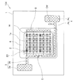
第1実施形態に係る発光装置100について、図1〜図4を参照しながら詳細に説明する。以下の説明では、まず発光装置100の全体構成について説明した後に、各構成について説明する。なお、説明の便宜上、図2における光反射樹脂6は、外形のみを線で示し、透過させた状態で図示している。他の実施形態で説明する図5〜図9についても、同様に透過させた状態で図示している。
[First Embodiment]
The
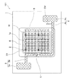
<全体構成>
発光装置100は、LED電球等の照明器具、表示装置、ディスプレイ、液晶ディスプレイのバックライト光源等に利用される装置である。発光装置100は、図1、図2および図4に示すように、基板1と、基板1の実装領域1aに複数配置された発光素子2と、基板1上に形成された正極3および負極4と、正極3に配置された保護素子5と、発光素子2や保護素子5等の電子部品と、正極3や負極4等を接続するワイヤWと、基板1上に形成された光反射樹脂6と、を主な構成として備えている。また、発光装置100は、ここでは光反射樹脂6内に封止部材7が充填された構成としている。
<Overall configuration>
The
<基板>
基板1は、発光素子2や保護素子5等の電子部品を配置するためのものである。基板1は、図1および図2に示すように、矩形平板状に形成されている。また、基板1上には、図2に示すように複数の発光素子2を配置するための実装領域1aが区画されている。なお、基板1のサイズは特に限定されず、発光素子2の数や配列間隔等、目的および用途に応じて適宜選択することができる。
<Board>
The substrate 1 is for arranging electronic components such as the
基板1の材料としては、絶縁性材料を用いることが好ましく、かつ、発光素子2から放出される光や外光等が透過しにくい材料を用いることが好ましい。また、ある程度の強度を有する材料を用いることが好ましい。具体的には、セラミックス(Al2O3、AlN等)、あるいはフェノール樹脂、エポキシ樹脂、ポリイミド樹脂、BTレジン(bismaleimide triazine resin)、ポリフタルアミド(PPA)等の樹脂が挙げられる。
As a material for the substrate 1, an insulating material is preferably used, and a material that hardly transmits light emitted from the light-emitting
<実装領域>
実装領域1aは、複数の発光素子2を配置するための領域である。実装領域1aは、図2に示すように、基板1の中央の領域に区画されている。実装領域1aは、互いに対向する辺を有する所定形状で形成されており、より具体的には、図2に示すように、角部を丸めた略矩形状に形成されている。なお、実装領域1aのサイズは特に限定されず、発光素子2の数や配列間隔等、目的および用途に応じて適宜選択することができる。
<Mounting area>
The mounting
実装領域1aの周囲には、図2を正面視した場合において、実装領域1aの左側の辺に沿って配線部3bの一部および配線部4bの一部が形成され、実装領域1aの下側の辺に沿って配線部4bの一部が形成され、実装領域1aの右側の辺に沿って中継配線部8が形成されている。なお、ここでの実装領域1aの周囲とは、図2に示すように、実装領域1aの周縁と所定の間隔を置いた周囲のことを意味している。
A part of the
実装領域1aは、複数の発光素子2を配置するために基板1上に区画した領域、すなわち基板1と同じ材料で構成された領域としてもよいが、例えば、実装領域1a上に光を反射する金属膜を形成し、当該金属膜を介して複数の発光素子2を配置することが好ましい。このように実装領域1a上に金属膜を形成してその上に複数の発光素子2を配置することで、例えば図4において、基板1の実装領域1a側に向う光も金属膜によって反射することができる。従って、出射光のロスを軽減することができ、発光装置100の光の取り出し効率を向上させることができる。
The mounting
実装領域1a上に形成する金属膜は、電解めっきまたは無電解めっきで形成することが好ましい。金属膜の材料としては、めっきができるものであれば特に限定されないが、例えば、Ag(銀)またはAu(金)を用いることが好ましく、特にAgを用いることが好ましい。Auは光を吸収しやすい特性を備えているが、例えばAuめっきの表面にTiO2膜をさらに形成することで、光反射率を高めることができる。また、AgはAuよりも光反射率が高いため、Au単独でめっきを行うよりも、発光装置100の光の取り出し効率を向上させることができる。なお、実装領域1a上に形成する金属膜の厚さは特に限定されず、目的および用途に応じて適宜選択することができる。
The metal film formed on the mounting
なお本実施形態では、図1および図4に示すように、実装領域1aの上部に後記する封止部材7が充填され、実装領域1a上の複数の発光素子2および、当該複数の発光素子2に接続されたワイヤWが塵芥、水分、外力等から保護される構成となっている。
In the present embodiment, as shown in FIGS. 1 and 4, a sealing
<発光素子>
発光素子2は、電圧を印加することで自発光する半導体素子である。発光素子2は、図2に示すように、基板1の実装領域1aに複数配置され、当該複数の発光素子2が一体となって発光装置100の発光部20を構成している。なお、発光素子2は、図示しない接合部材によって実装領域1aに接合されており、その接合方法としては、例えば接合部材として樹脂や半田ペーストを用いる接合方法を用いることができる。なお、図示された発光部20は単に発光素子2を載置させる領域を示すものであり、発光部20における発光とは、発光素子2から出される光であることはいうまでもない。
<Light emitting element>
The
発光素子2のそれぞれは、図3に示すように、矩形状に形成されている。また、発光素子2は、図3に示すように、その上面の一側にp電極2Aが設けられ、発光素子2の他側にn電極2Bが設けられたフェースアップ(FU)素子である。本実施形態では、発光素子2を載置する実装領域1a上の金属膜と、正極3および負極4を構成する金属部材と、を離間して配置するため、図3に示すように、p電極2Aとn電極2Bが同一面側に形成された発光素子2を用い、電極形成面と反対側の面を実装領域1a上の金属膜に接着することが好ましい。
Each of the
p電極2Aおよびn電極2Bは、図3に示すように、電極端子であるpパッド電極2Aaおよびnパッド電極2Baと、発光素子2に投入された電流を全体に拡散させるための補助電極である延伸導電部2Ab,2Bbと、をそれぞれ備えている。なお、発光素子2は少なくともpパッド電極2Aaとnパッド電極2Baが同一面側にあればよく、延伸導電部2Ab,2Bbを設けなくてもよい。また、図示は省略したが、発光素子2は、側面視すると、n型半導体層およびp型半導体層からなる複数の半導体層が積層された構造を有している。
As shown in FIG. 3, the
発光素子2としては、具体的には発光ダイオードを用いるのが好ましく、用途に応じて任意の波長のものを選択することができる。例えば、青色(波長430nm〜490nmの光)、緑色(波長490nm〜570nmの光)の発光素子2としては、ZnSe、窒化物系半導体(InXAlYGa1−X−YN、0≦X、0≦Y、X+Y≦1)、GaP等を用いることができる。また、赤色(波長620nm〜750nmの光)の発光素子2としては、GaAlAs、AlInGaP等を用いることができる。
Specifically, a light-emitting diode is preferably used as the light-emitting
また、後記するように、封止部材7(図1参照)に蛍光物質を導入する場合は、その蛍光物質を効率良く励起できる短波長の発光が可能な窒化物半導体(InXAlYGa1−X−YN、0≦X、0≦Y、X+Y≦1)を用いることが好ましい。ただし、発光素子2の成分組成や発光色、サイズ等は上記に限定されず、目的に応じて適宜選択することができる。また、発光素子2は、可視光領域の光だけではなく、紫外線や赤外線を出力する素子で構成することもできる。また、高出力化のためには、発光素子2の個数は、例えば10個以上、20〜150個の範囲内とすることが好ましい。
As will be described later, when a fluorescent material is introduced into the sealing member 7 (see FIG. 1), a nitride semiconductor (In X Al Y Ga 1 capable of emitting light of a short wavelength that can efficiently excite the fluorescent material). -X-YN , 0≤X, 0≤Y, X + Y≤1) are preferably used. However, the component composition, emission color, size, and the like of the
発光素子2は、図2に示すように、実装領域1a上において、縦方向および横方向にそれぞれ等間隔で配列されており、ここでは、縦8個×横5個の合計40個配置されている。また、発光素子2は、図2に示すように、実装領域1aに対して横方向に隣り合う発光素子2同士が導電性のワイヤWによって電気的に接続され、直列接続されている。なお、ここでの直列接続とは、図2に示すように、隣り合う発光素子2におけるp電極2Aとn電極2BとがワイヤWによって電気的に接続された状態を意味している。
As shown in FIG. 2, the
発光素子2は、図2に示すように、正極3の配線部3bと中継配線部8との間においては、複数の発光素子2のp電極2Aが実装領域1aの一方向である左側を向くように、あるいは、複数の発光素子2のn電極2Bが実装領域1aの他方向である右側を向くように配列されている。
As shown in FIG. 2, in the
また、発光素子2は、図2に示すように、負極4の配線部4bと中継配線部8との間においては、複数の発光素子2のp電極2Aが実装領域1aの他方向である右側を向くように、かつ、複数の発光素子2のn電極2Bが実装領域1aの一方向である左側を向くように、配列されている。すなわち、発光素子2は、図2を平面視した場合において、上方グループ(領域)と下方のグループ(領域)とにおいて、中継配線部8の中央を境に向きが反転するように配置されている。
In addition, as shown in FIG. 2, the
実施形態に係る発光装置100においては、このように実装領域1aの周囲に沿って中継配線部8を形成し、かつ、当該中継配線部8の中央を境に向きが反転するように発光素子2を配置することで、発光素子2同士を接続する配線が複雑になることなく、実装領域1aの限られた面積内において、直列接続される発光素子2の数を増加させることができる。さらには、実装領域1aの限られた面積内において、複数の発光素子2を密に配置することができ、一定の輝度に対して消費電力が向上した発光装置100を、または一定の消費電力に対して発光効率が向上した発光装置100を得ることができる。なお、実施形態に係る発光装置100においては、図2に示すように、発光素子2が10個直列接続されるとともに、当該直列接続が4列分形成されている。
In the
<正極および負極>
正極3および負極4は、基板1上の複数の発光素子2や保護素子5等の電子部品と、図示しない外部電源とを電気的に接続し、これらの電子部品に対して外部電源からの電圧を印加するためのものである。すなわち、正極3および負極4は、外部から通電させるための電極、またはその一部としての役割を担うものである。
<Positive electrode and negative electrode>
The
正極3および負極4は、図2に示すように、基板1上の金属部材で構成されている。正極3および負極4は、図2に示すように略矩形状のパッド部(給電部)3a,4aと、線状の配線部3b,4bと、を有しており、パッド部3a,4aに印加された電圧が配線部3b,4bを介して複数の発光素子2からなる発光部20へと印加されるように構成されている。なお、負極4の配線部4bには、図2に示すように、カソードであることを示すカソードマークCMが形成されている。
The
パッド部3a,4aは、外部電源からの電圧が印加されるためのものである。パッド部3a,4aは、図2に示すように、基板1上の角部における対角線の位置に、一対で形成されている。そして、パッド部3a,4aは、導電性のワイヤWによって、図示しない外部電源と電気的に接続されている。
The
配線部3b,4bは、外部電源からパッド部3a,4aに印加された電圧を、実装領域1a上の発光素子2へと伝達するためのものである。配線部3b,4bは、図2に示すように、パッド部3a,4aから延出するように形成されるとともに、実装領域1aの周囲に略L字状で形成されている。
The
配線部3bの一端部と、配線部4bの一端部とは、図2に示すように、実装領域1aの周囲において互いに隣り合うように形成されている。このように、正極3および負極4の配線部3b,4bを実装領域1aの周囲に沿って形成し、かつ、その一端部を隣り合わせて形成することで、発光装置100のように複数の発光素子2を基板1上に配置した場合であっても、後記する保護素子5を適切な位置に配置することができる。従って、正負両電極間の電圧がツェナー電圧以上となることを防止することができ、過大な電圧が印加されることによる発光素子2の素子破壊や性能劣化の発生を適切に防止することができる。
As shown in FIG. 2, one end of the
配線部3b,4bは、より具体的には、図2に示す略矩形状の実装領域1aの一辺の範囲内において、その一端部が互いに隣り合うように形成されることが好ましい。このように、実装領域1aの一辺の範囲内で隣り合うように配線部3b,4bを形成することで、配線部3b,4bと発光素子2とを電気的に接続するためのワイヤWの設置面積を確保することができる。そのため、配線部3b,4bと接続する発光素子2の数、すなわち直列接続の始点および終点となる発光素子2の数を増やすことができ、実装領域1a上における発光素子2の直列接続の列数を増加させることができる。そして、このように直列接続の列数を増加させることで、実装領域1aの限られた面積内において、複数の発光素子2を密に配置することができ、一定の輝度に対して消費電力が向上した発光装置100を、または一定の消費電力に対して発光効率が向上した発光装置100を得ることができる。
More specifically, the
なお、配線部3b,4bは、図2に示す略矩形状の実装領域1aの一辺の範囲内における中間地点において、その一端部が互いに隣り合うように形成されることがより好ましい。これにより、図2に示すように、配線部3bおよび中継配線部8間における直列接続の列数と、配線部4bと中継配線部8間における直列接続の列数を揃えることができるため、実装領域1aの限られた面積内において、複数の発光素子2を密に配置することができ、一定の輝度に対して消費電力が向上した発光装置100を、または一定の消費電力に対して発光効率が向上した発光装置100を得ることができる。
The
正極3および負極4を構成する金属部材の素材は、Auを用いることが好ましい。これは、後記するように、ワイヤWの材料として熱伝導性が向上したAuを用いた場合に、同素材であるワイヤWを強固に接合することができるためである。
It is preferable to use Au as the material of the metal member constituting the
正極3および負極4を構成する金属部材の形成方法としては、前記した実装領域1a上の金属膜の形成方法と同様に、電解めっきまたは無電解めっきで形成することが好ましい。なお、正極3および負極4を構成する金属部材の厚さは特に限定されず、ワイヤWの数等、目的および用途に応じて適宜選択することができる。
As a method for forming the metal member constituting the
ここで、配線部3b,4bの一部は、図1および図2に示すように、後記する光反射樹脂6によって覆われている。そのため、配線部3b,4bを、前記したように光を吸収しやすいAuで形成した場合であっても、発光素子2から出射された光が配線部3b,4bには到達せずに光反射樹脂6によって反射される。従って、出射光のロスを軽減することができ、発光装置100の光の取り出し効率を向上させることができる。
Here, as shown in FIGS. 1 and 2, a part of the
さらに、配線部3b,4bの一部を光反射樹脂6によって覆うことにより、当該ワイヤWを塵芥、水分、外力等から保護することができる。なお、ここでの配線部3b,4bの一部とは、図2に示すように、配線部3b,4bのうちで、実装領域1aの周囲であって、実装領域1aの辺に沿って形成された部分のことを意味している。
Furthermore, by covering a part of the
このように発光装置100は、正極3および負極4および中継配線部8を、実装領域1aの周囲に沿って設け、正極3および負極4および中継配線部8と実装領域1aとを、基板1上で離間して設ける。このように構成することで、発光装置100は、正極3、負極4、中継配線部8においてはワイヤWを強固に接合できる素材(例えばAu)を用い、実装領域1aには光反射率の高い素材(Ag)を用いることが、それぞれにおいて可能になるため、光取り出し効率の向上した信頼性の高い発光装置を得ることができる。
As described above, the
<保護素子>
保護素子5は、複数の発光素子2からなる発光部20を、過大な電圧印加による素子破壊や性能劣化から保護するための素子である。保護素子5は、図2に示すように、正極3の配線部3bの一端部に配置され、負極4の配線部4bの一端部とワイヤWで接続される。ただし、保護素子5は、負極4の配線部4bの一端部に配置され、正極3の配線部3bの一端部とワイヤWで接続されていてもよい。
<Protective element>
The
保護素子5は、具体的には、規定電圧以上の電圧が印加されると通電状態になるツェナーダイオード(Zener Diode)で構成される。保護素子5は、図示は省略したが、前記した発光素子2と同様にp電極とn電極とを有する半導体素子であり、発光素子2のp電極2Aとn電極2Bに対して逆並列となるように、ワイヤWによって負極4の配線部4bと電気的に接続される。なお、保護素子5が配置された場所の近傍には発光素子2を配置することができない。従って、保護素子5に最も近い4行1列目の発光素子2は、図2に示すように、保護素子5が配置された領域から離れた場所にワイヤWによって接続される。
Specifically, the
この保護素子5があることにより、正極3と負極4との間に過大な電圧が印加されてその電圧がツェナーダイオードのツェナー電圧を超えたとしても、発光素子2の正負両電極間がツェナー電圧に保持され、このツェナー電圧以上になることがない。従って、保護素子5を備えることによって、正負両電極間の電圧がツェナー電圧以上となることを防止することができ、過大な電圧が印加されることによる発光素子2の素子破壊や性能劣化の発生を適切に防止することができる。
Due to the presence of the
保護素子5は、図2に示すように、後記する光反射樹脂6によって覆われている。従って、保護素子5および保護素子5に接続されるワイヤWが、塵芥、水分、外力等から保護される。なお、保護素子5のサイズは特に限定されず、目的および用途に応じて適宜選択することができる。
As shown in FIG. 2, the
<光反射樹脂>
光反射樹脂6は、発光素子2から出射された光を反射させるためのものである。光反射樹脂6は、図2に示すように、配線部3b,4bの一部、中継配線部8、保護素子5およびこれらに接続されるワイヤWを覆うように形成される。そのため、配線部3b,4b、中継配線部8およびワイヤWを、前記あるいは後記したように光を吸収しやすいAuで形成した場合であっても、発光素子2から出射された光が配線部3b,4b、中継配線部8およびワイヤWには到達せずに光反射樹脂6によって反射される。従って、出射光のロスを軽減することができ、発光装置100の光の取り出し効率を向上させることができる。さらに、配線部3b,4bの一部、中継配線部8、保護素子5およびこれらに接続されるワイヤWを光反射樹脂6によって覆うことによって、これらの部材を塵芥、水分、外力等から保護することができる。
<Light reflecting resin>
The
光反射樹脂6は、図1および図2に示すように、基板1上において発光部20が形成された実装領域1aを囲うように四角枠状に形成されることが好ましい。このように実装領域1aの周囲を囲うように光反射樹脂6を形成することで、例えば図4の左右両側に配置された発光素子2から出射された光のように、基板1の実装領域1aの周囲に向う光も光反射樹脂6によって反射することができる。従って、出射光のロスを軽減することができ、発光装置100の光の取り出し効率を向上させることができる。
As shown in FIGS. 1 and 2, the
また、光反射樹脂6は、図2に示すように、実装領域1aの周縁となる領域の一部を覆うように形成することが好ましい。このように、実装領域1aの周縁の一部を覆うように光反射樹脂6を形成することで、配線部3b,4bと実装領域1a上の金属膜との間に基板1が露出した領域が形成されることがなくなる。従って、発光素子2から出射された光を、光反射樹脂6が形成された内部の領域において全て反射させることができるため、出射光のロスを最大限軽減することができ、発光装置100の光の取り出し効率をより向上させることができる。
Further, as shown in FIG. 2, the
光反射樹脂6の材料としては、絶縁材料を用いることが好ましい。また、ある程度の強度を確保するために、例えば熱硬化性樹脂、熱可塑性樹脂等を用いることができる。より具体的には、フェノール樹脂、エポキシ樹脂、BTレジンや、PPAやシリコン樹脂などが挙げられる。また、これらの母体となる樹脂に、発光素子2からの光を吸収しにくく、かつ母体となる樹脂に対する屈折率差の大きい反射部材(例えばTiO2,Al2O3,ZrO2,MgO)等の粉末を分散することで、効率よく光を反射させることができる。なお、光反射樹脂6のサイズは特に限定されず、目的および用途に応じて適宜選択することができる。また、光反射樹脂6の位置に、樹脂と異なる材料からなる光反射部材を形成することもできる。
As a material of the
<封止部材>
封止部材7は、基板1に配置された発光素子2、保護素子5およびワイヤW等を、塵芥、水分、外力等から保護するための部材である。封止部材7は、図1、図2および図4に示すように、基板1上において、光反射樹脂6で囲った実装領域1a内に樹脂を充填することで形成される。
<Sealing member>
The sealing
封止部材7の材料としては、発光素子2からの光を透過可能な透光性を有するものが好ましい。具体的な材料としては、シリコン樹脂、エポキシ樹脂、ユリア樹脂等を挙げることができる。また、このような材料に加えて、所望に応じて着色剤、光拡散剤、フィラー、蛍光部材等を含有させることもできる。
As the material of the sealing
なお、封止部材7は、単一の部材で形成することもできるし、あるいは、2層以上の複数の層として形成することもできる。また、封止部材7の充填量は、光反射樹脂6で囲った実装領域1a内に配置される発光素子2、保護素子5、ワイヤW等が被覆される量であればよい。また、封止部材7にレンズ機能をもたせる場合は、封止部材7の表面を盛り上がらせて砲弾型形状や凸レンズ形状としてもよい。
The sealing
<蛍光部材>
封止部材7中に、波長変換部材として発光素子2からの光の少なくとも一部を吸収して異なる波長を有する光を発する蛍光部材を含有させることもできる。蛍光部材としては、発光素子2からの光をより長波長に変換させるものが好ましい。また、蛍光部材は1種の蛍光物質等を単層で形成してもよいし、2種以上の蛍光物質等が混合されたものを単層として形成してもよい。あるいは、1種の蛍光物質等を含有する単層を2層以上積層させてもよいし、2種以上の蛍光物質等がそれぞれ混合された単層を2層以上積層させてもよい。
<Fluorescent member>
The sealing
蛍光部材の材料としては、例えばイットリウム、アルミニウムおよびガーネットを混合したYAG系蛍光体、Eu,Ce等のランタノイド系元素で主に賦活される、窒化物系蛍光体、酸窒化物系蛍光体を用いることができる。 As the material of the fluorescent member, for example, a YAG phosphor mixed with yttrium, aluminum and garnet, a nitride phosphor or an oxynitride phosphor mainly activated by a lanthanoid element such as Eu or Ce is used. be able to.
<中継配線部>
中継配線部8は、正極3と負極4の間における配線を中継するためのものである。中継配線部8は、図2に示すように、基板1上の金属部材で構成されている。中継配線部8は、図2に示すように、実装領域1aの周囲において、当該実装領域1aの一辺、すなわち右側の辺に沿って直線状に形成されている。
<Relay wiring section>
The
中継配線部8は、図2に示すように、光反射樹脂6によって覆われている。そのため、後記するように、中継配線部8を構成する金属部材として光を吸収しやすいAuを用いた場合であっても、発光素子2から出射された光は中継配線部8には到達せずに光反射樹脂6によって反射される。従って、出射光のロスを軽減することができ、発光装置100の光の取り出し効率を向上させることができる。さらに、中継配線部8を光反射樹脂6によって覆うことにより、当該中継配線部8を塵芥、水分、外力等から保護することができる。
As shown in FIG. 2, the
中継配線部8を構成する金属部材の素材は、正極3および負極4と同様に、Auを用いることが好ましい。これは、後記するように、ワイヤWの材料として熱伝導性が向上したAuを用いた場合に、同素材であるワイヤWを強固に接合することができるためである。
As with the
中継配線部8を構成する金属部材の形成方法としては、正極3および負極4と同様に、電解めっきまたは無電解めっきで形成することが好ましい。なお、中継配線部8を構成する金属部材の厚さは特に限定されず、ワイヤWの数等、目的および用途に応じて適宜選択することができる。
As a method for forming the metal member constituting the
実施形態に係る発光装置100においては、このように実装領域1aの周囲に沿って中継配線部8を形成し、かつ、当該中継配線部8を境に向きが反転するように発光素子2を配置することで、発光素子2同士を接続する配線が複雑になることなく、実装領域1aの限られた面積内において、直列接続される発光素子2の数を増加させることができる。さらには、実装領域1aの限られた面積内において、複数の発光素子2を密に配置することができ、一定の輝度に対して消費電力が向上した発光装置100を、または一定の消費電力に対して発光効率が向上した発光装置100を得ることができる。
In the
<ワイヤ>
ワイヤWは、発光素子2や保護素子5等の電子部品と、正極3、負極4および中継配線部8等を電気的に接続するための導電性の配線である。ワイヤWの材料としては、Au、Cu(銅)、Pt(白金)、Al(アルミニウム)等の金属、および、それらの合金を用いたものが挙げられるが、特に、熱伝導率等に優れたAuを用いるのが好ましい。なお、ワイヤWの径は特に限定されず、目的および用途に応じて適宜選択することができる。
<Wire>
The wire W is a conductive wiring for electrically connecting electronic components such as the
ここで、ワイヤWと、正極3、負極4および中継配線部8との接続部分は、図2に示すように、光反射樹脂6によって覆われている。そのため、前記したように、ワイヤWを構成する材料として光を吸収しやすいAuを用いた場合であっても、発光素子2から出射された光はワイヤWには吸収されずに光反射樹脂6によって反射される。従って、出射光のロスを軽減することができ、発光装置100の光の取り出し効率を向上させることができる。さらに、ワイヤWと、正極3、負極4および中継配線部8との接続部分を光反射樹脂6によって覆うことにより、当該ワイヤWを塵芥、水分、外力等から保護することができる。なお、発光装置100から取り出される光とは、図1または図4に示されるように、光反射樹脂6に囲まれた封止部材7の表面から取り出される光である。つまり発光装置100でみて、封止部材7の表面が発光面となる。
Here, the connection part of the wire W and the
[発光装置の動作]
以上説明した発光装置100によれば、発光装置100を駆動した時に、発光素子2からあらゆる方向に進む光のうち、上方に進む光は発光装置100の上方の外部に取り出される。また、下方や横方向等に進む光は、基板1の実装領域1aにおける底面や側面で反射して、発光装置100の上方に取り出されることになる。この時、基板1の底面、すなわち実装領域1aには好ましくは金属膜が被覆され、実装領域1aの周囲には光反射樹脂6が形成されているため、この部位による光の吸収が抑制されるとともに、金属膜や光反射樹脂6により光が反射される。これにより、発光素子2からの光が効率良く取り出される。また、発光装置100は、中継配線部8により直列接続される発光素子2の数を増加させることができるため、一定の輝度に対して消費電力を向上させる、あるいは、一定の消費電力に対して発光効率を向上させることができる。
[Operation of light emitting device]
According to the
[発光装置の製造方法]
次に、本発明の第1の実施形態に係る発光装置100の製造方法について、簡単に説明する。発光装置100の製造方法は、基板作製工程と、めっき工程と、ダイボンディング工程と、ワイヤボンディング工程と、光反射樹脂形成工程と、を含む。また、光反射樹脂形成工程の後に、封止部材充填工程を含んでもよい。さらにここでは、保護素子接合工程を含む。以下、各工程について説明する。なお、発光装置100の構成については前記説明した通りであるので、ここでは適宜、説明を省略する。
[Method for Manufacturing Light Emitting Device]
Next, a method for manufacturing the
<基板作製工程>
基板作製工程は、めっき用配線が形成された基板1を作製する工程である。基板作製工程では、基板1上の実装領域1aや、正極3および負極4となる部位を所定の形状にパターニングすることで形成する。また、基板作製工程では、電解めっきによって基板1上の実装領域1aに金属膜を形成するためのめっき用配線を形成する。
<Substrate manufacturing process>
A board | substrate preparation process is a process of producing the board | substrate 1 with which the wiring for plating was formed. In the substrate manufacturing process, the mounting
<めっき工程>
めっき工程は、前記めっき配線が形成された基板1上に、少なくとも正極3および負極4を構成する金属部材を形成する工程であり、好ましくは無電解めっきにより正極3および負極4を構成する金属部材を形成するとともに、基板1上の実装領域1a上に、電解めっきにより金属膜を形成する工程である。また、中継配線部8を設ける場合、正極3および負極4と同様の工程で金属部材が形成される。
<Plating process>
The plating step is a step of forming a metal member constituting at least the
めっきの具体的な方法としては、正極3および負極4と実装領域1a上の金属膜の両方にAuめっきを行う方法、正極3および負極4のみにAuめっきを行い、実装領域1a上の金属膜を形成しない方法、正極3および負極4にAuめっきを行い、実装領域1a上にAgめっきを行う方法、等が挙げられる。また、実装領域1a上には、AuめっきやAgめっきを行う場合はAuまたはAgの表面に、まためっきを行わない場合は直接基板1表面に、さらにTiO2膜を形成することが好ましい。
As a specific method of plating, a method of performing Au plating on both the
<ダイボンディング工程>
ダイボンディング工程は、前記金属膜上に発光素子2を載置する工程である。ダイボンディング工程は、実装領域1a上の金属膜に、接合部材を介して、発光素子2を載置する発光素子載置工程と、発光素子2を載置した後に、接合部材を加熱し、発光素子2を実装領域1a上の金属膜上に接合する加熱工程と、を行う。
<Die bonding process>
The die bonding step is a step of placing the
<保護素子接合工程>
保護素子接合工程は、前記正極3の配線部3b上に保護素子5を載置して接合する工程である。保護素子5を載置、接合する方法は、前記ダイボンディング工程と同様であるので、ここでは説明を省略する。
<Protective element bonding process>
The protective element bonding step is a step of mounting and bonding the
<ワイヤボンディング工程>
ワイヤボンディング工程は、前記ダイボンディング工程の後に、金属部材の正極3の配線部3bと、発光素子2上部にあるpパッド電極2Aaとを、ワイヤWで電気的に接続する工程である。同じく、発光素子2上部にあるnパッド電極2Baと、金属部材の負極4の配線部4bと、をワイヤWで電気的に接続する工程である。さらに、この工程では、複数の発光素子2をそれぞれpパッド電極2Aaおよびnパッド電極2Baを介して接続する。また、保護素子5と負極4との電気的な接続もこの工程で行えばよい。すなわち、保護素子5のn電極と、負極4の配線部4bとをワイヤWで接続する。なお、ワイヤWの接続方法は、特に限定されるものではなく、通常用いられる方法で行えばよい。
<Wire bonding process>
The wire bonding step is a step of electrically connecting the
<光反射樹脂形成工程>
光反射樹脂形成工程は、前記ワイヤボンディング工程の後に、前記実装領域1aの周縁に沿って、少なくとも配線部3b,4bの一部および中継配線部8を覆うように光反射樹脂6を形成する工程である。光反射樹脂6の形成は、例えば、固定された基板1の上側において、基板1に対して上下方向あるいは水平方向などに移動(可動)させることができる樹脂吐出装置を用いて行うことができる(特開2009−182307号公報参照)。
<Light reflecting resin formation process>
The light reflecting resin forming step is a step of forming the
<封止部材充填工程>
封止部材充填工程は、前記光反射樹脂6の内側に、前記発光素子2および前記金属膜を被覆する透光性の封止部材7を充填する工程である。すなわち、発光素子2、保護素子5、実装領域1a上の金属膜およびワイヤW等を被覆する封止部材7を、基板1上に形成された光反射樹脂6からなる壁部の内部に溶融樹脂を注入し、その後加熱や光照射等によって硬化する工程である。
<Sealing member filling process>
The sealing member filling step is a step of filling a light-transmitting
[第2実施形態]
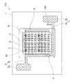
第2実施形態に係る発光装置101について、図5を参照しながら詳細に説明する。発光装置101は、図5に示すように、ワイヤWの配線状態以外は、前記した第1実施形態に係る発光装置100と同様の構成を備えている。従って、前記した発光装置100と重複する構成については、同じ符号を付して説明を省略する。また、発光装置101は、前記した発光装置100と、全体構成(図1)および発光素子の構成(図3)が同じであるため、これらについても説明を省略する。
[Second Embodiment]
The
発光装置101は、図5に示すように、実装領域1aに対して横方向および縦方向に隣り合う発光素子2同士が導電性のワイヤWによって電気的に接続され、直列接続および並列接続されている。なお、ここでの並列接続とは、図5に示すように、隣り合う発光素子2におけるp電極2A同士またはn電極2B同士がワイヤWによって電気的に接続された状態を意味している。
As shown in FIG. 5, in the
このように、複数の発光素子2同士を直列のみならず並列に接続することで、仮に複数の発光素子2ごとの順方向降下電圧(以下、Vfという)にばらつきがある場合であっても、そのVfのばらつきを解消することができる。なお、Vfとは、発光ダイオードに対して順方向に電流を流すために必要な電圧、すなわち発光ダイオードが光を照射するために必要な電圧のことをいう。
In this way, even when the plurality of
ここで、複数の発光素子2ごとのVfのばらつきがあると、Vfの低い発光素子2に電流が流れやすくなり、発光素子2間に出力の違いが生じて発光ムラが発生しやすい。そこで、前記したように、複数の発光素子2同士を並列接続することにより、並列接続された発光素子2間のVfのばらつきによる各発光素子2の出力差を軽減することができ、発光ムラを抑制することができる。
Here, if there is a variation in V f for each of the plurality of
なお、前記したように複数の発光素子2を並列接続する場合は、図5に示すように、複数の発光素子2のうち、配線部3b,4bおよび中継配線部8と直接接続される発光素子2同士は、並列接続を行わないことが好ましい。すなわち、発光装置101においては、配線部3bと直接接続される実装領域1a上の1行1列目、2行1列目の発光素子2のp電極2A、配線部4bと直接接続される実装領域1a上の7行1列目、8行1列目の発光素子2のn電極2B、中継配線部8と直接接続される1行5列目、2行5列目、3行5列目、4行5列目のn電極2B、中継配線部8と直接接続される5行5列目、6行5列目、7行5列目、8行5列目のp電極2Aは、並列接続されていない。これにより、ワイヤWによってかかる負荷を軽減することができる。
In addition, when connecting the some
[第3実施形態]
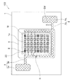
第3実施形態に係る発光装置102について、図6を参照しながら詳細に説明する。発光装置102は、図6に示すように、配線部3b,4bの形状とワイヤWの配線状態以外は、前記した第1実施形態に係る発光装置100と同様の構成を備えている。従って、前記した発光装置100と重複する構成については、同じ符号を付して説明を省略する。また、発光装置102は、前記した発光装置100と、全体構成(図1)および発光素子の構成(図3)が同じであるため、これらについても説明を省略する。
[Third Embodiment]
The
発光装置102は、図6に示すように、配線部3b,4bの一端部が、略矩形状の実装領域1aの角部において、互いに隣り合うように形成されている。すなわち、配線部3bは、パッド部3aから実装領域1aの角部まで延出するように略L字状に形成されている。また、配線部4bは、パッド部4aから実装領域1aの角部まで延出するように直線状に形成されている。
As shown in FIG. 6, the
このような構成を備える発光装置102は、実装領域1aの周囲に沿って中継配線部8を形成し、かつ、当該中継配線部8を境に向きが反転するように発光素子2を配置することで、実装領域1aの限られた面積内において、発光素子2同士を接続する配線が複雑になることなく、直列接続される発光素子2の数を増加させることができる。さらには、実装領域1aの限られた面積内において、複数の発光素子2を密に配置することができ、一定の輝度に対して消費電力が向上した発光装置100を、または一定の消費電力に対して発光効率が向上した発光装置100を得ることができる。また、複数の発光素子2同士を直列のみならず並列に接続することで、仮に複数の発光素子2ごとのVfにばらつきがある場合であっても、そのVfのばらつきを解消することができる。
In the
[第4実施形態]
第4実施形態に係る発光装置103について、図7を参照しながら詳細に説明する。発光装置103は、図7に示すように、配線部4bの形状とワイヤWの配線状態以外は、前記した第1実施形態に係る発光装置100と同様の構成を備えている。従って、前記した発光装置100と重複する構成については、同じ符号を付して説明を省略する。また、発光装置103は、前記した発光装置100と、全体構成(図1)および発光素子の構成(図3)が同じであるため、これらについても説明を省略する。
[Fourth Embodiment]
The
発光装置103は、図7に示すように、配線部3bの一端部と、配線部4bの一端部とが、実装領域1aの周囲において互いに隣り合うように形成されている。また、正極3および負極4と独立した中継配線部8がなく、実装領域1aの周囲であって、かつ、当該実装領域1aの一辺である右側の辺に沿って、負極4の配線部4bを延出させている。
As shown in FIG. 7, the
このような構成を備える発光装置103は、正極3および負極4の配線部3b,4bを実装領域1aの周囲に沿って形成し、かつ、その一端部を隣り合わせて形成することで、発光装置103のように複数の発光素子2を基板1上に配置した場合であっても、後記する保護素子5を適切な位置に配置することができる。従って、正負両電極間の電圧がツェナー電圧以上となることを防止することができ、過大な電圧が印加されることによる発光素子2の素子破壊や性能劣化の発生を適切に防止することができる。
In the
[第5実施形態]
第5実施形態に係る発光装置104について、図8を参照しながら詳細に説明する。発光装置104は、図8に示すように、ワイヤWの配線状態以外は、前記した第2実施形態に係る発光装置101と同様の構成を備えている。従って、前記した発光装置101と重複する構成については、同じ符号を付して説明を省略する。また、発光装置104は、前記した発光装置101と、全体構成(図1)および発光素子の構成(図3)が同じであるため、これらについても説明を省略する。
[Fifth Embodiment]
The
発光装置104は、図8に示すように、配線部3bおよび中継配線部8を繋ぐ配線と、配線部4bおよび中継配線部8を繋ぐ配線と、がそれぞれはしご状配線(ラダー配線)で構成されている。このような構成を備える発光装置104は、複数の発光素子2同士を直列のみならず並列に接続することで、複数の発光素子2ごとのVfのばらつきを解消することができる。
As shown in FIG. 8, the
[第6実施形態]
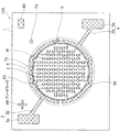
第6実施形態に係る発光装置105について、図9を参照しながら詳細に説明する。発光装置105は、図9に示すように、実装領域1aの形状および配線部3b,4bの形状以外は、前記した第1実施形態に係る発光装置100とほぼ同様の構成を備えている。従って、前記した発光装置100と重複する構成については、同じ符号を付して説明を省略する。また、発光装置105は、前記した発光装置100と、発光素子の構成(図3)が同じであるため、これらについても説明を省略する。
[Sixth Embodiment]
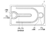
The
発光装置105は、発光装置100では略矩形状に形成された実装領域1aが、図9に示すように、円形状に形成されている。この円形状の実装領域1aには、図9に示すように、複数の発光素子2が縦方向および横方向にそれぞれ等間隔で配列されている。また、複数の発光素子2は、図9に示すように、ここでは、縦方向に最大で10個、最小で3個配置されるとともに、横方向に最大で14個、最小で6個配置され、合計110個配置されている。また、正極3および負極4の配線部3b,4bは、図9に示すように、当該円形状の実装領域の周囲に沿って形成され、それぞれの一端部が互いに隣り合うように形成されている。
In the
光反射樹脂6は、基板1上において発光部20が形成された実装領域1aを囲うように円状に形成されている。また、光反射樹脂6は、配線部3b,4bの一部、保護素子5およびこれらに接続されるワイヤWを覆うように形成されている。なお、符号AMはパッド部3aが正極3であることを示すアノードマーク、符号30は、実装領域上に形成された金属膜、符号70は、発光素子2のボンディング位置を認識するための認識マーク、符号80は発光装置104の温度計測ポイントであり、これらもめっき等により形成される。
The
このような構成を備える発光装置105は、正極3および負極4の配線部3b,4bを円形状の実装領域1aの周囲に沿って形成し、かつ、その一端部を隣り合わせて形成することで、発光装置105のように複数の発光素子2を基板1上における円形状の実装領域1aに配置した場合であっても、前記した保護素子5を適切な位置に配置することができる。従って、発光装置105は、正負両電極間の電圧がツェナー電圧以上となることを防止することができ、過大な電圧が印加されることによる発光素子2の素子破壊や性能劣化の発生を適切に防止することができる。
In the
以上、本発明に係る発光装置について、発明を実施するための形態により具体的に説明したが、本発明の趣旨はこれらの記載に限定されるものではなく、特許請求の範囲の記載に基づいて広く解釈されなければならない。また、これらの記載に基づいて種々変更、改変等したものも本発明の趣旨に含まれることはいうまでもない。 The light emitting device according to the present invention has been specifically described above with reference to embodiments for carrying out the invention. However, the gist of the present invention is not limited to these descriptions, and is based on the description of the claims. It must be interpreted widely. Needless to say, various changes and modifications based on these descriptions are also included in the spirit of the present invention.
1 基板
1a 実装領域
2 発光素子
2A p電極
2Aa pパッド電極
2Ab 延伸導電部
2B n電極
2Ba nパッド電極
2Bb 延伸導電部
3 正極
3a パッド部
3b 配線部
4 負極
4a パッド部
4b 配線部
5 保護素子
6 光反射樹脂
7 封止部材
8 中継配線部
20 発光部
30 金属膜
70 認識マーク
80 温度計測ポイント
100,101,102,103,104,105 発光装置
AM アノードマーク
CM カソードマーク
Vf 順方向降下電圧
W ワイヤ
DESCRIPTION OF SYMBOLS 1 Board |
Claims (7)
前記基板上の実装領域に配置された複数の発光素子からなる発光部と、
それぞれがパッド部と配線部とを有し、当該配線部を介して前記発光部に電圧を印加する正極および負極と、
前記正極または前記負極のいずれか一方に配置されるとともに、前記正極または前記負極のいずれか他方と電気的に接続された保護素子と、
少なくとも前記配線部および前記保護素子を覆うように前記基板上に形成された光反射樹脂と、を備える発光装置であって、
前記正極の配線部および前記負極の配線部は、前記実装領域の周囲に沿って形成され、かつ、その一端部が互いに隣り合うように形成され、
前記実装領域は、円形状に形成され、
前記正極の配線部と前記負極の配線部とは、当該円形状の実装領域の周囲において、その一端部が互いに隣り合うように形成され、
前記保護素子が、前記互いに隣り合うように形成された前記正極と前記負極とのうちの一方の前記配線部の一端部に配置されワイヤで他方の前記配線部の一端部と接続されたことを特徴とする発光装置。 A substrate,
A light-emitting portion composed of a plurality of light-emitting elements disposed in a mounting region on the substrate;
Each having a pad portion and a wiring portion, and a positive electrode and a negative electrode for applying a voltage to the light emitting portion through the wiring portion;
A protective element disposed on either the positive electrode or the negative electrode and electrically connected to either the positive electrode or the negative electrode;
A light reflecting device formed on the substrate so as to cover at least the wiring portion and the protection element,
The positive wiring portion and the negative wiring portion are formed along the periphery of the mounting region, and are formed so that one end portions thereof are adjacent to each other,
The mounting area is formed in a circular shape,
The positive electrode wiring portion and the negative electrode wiring portion are formed so that one end portions thereof are adjacent to each other around the circular mounting region,
The protective element is disposed at one end portion of the wiring portion of one of the positive electrode and the negative electrode formed so as to be adjacent to each other, and is connected to one end portion of the other wiring portion by a wire. A light emitting device characterized.
平面視で、前記光反射樹脂によって覆われていない前記1つの電極の前記一部は、前記光反射樹脂によって覆われた前記1つの電極の前記配線部の前記一部より前記実装領域から離れていることを特徴とする請求項1に記載の発光装置。 With respect to one electrode of the positive electrode or the negative electrode, a part of the one electrode is not covered with the light reflecting resin, and at least one of the wiring portions of either the positive electrode or the negative electrode. The part is covered with the light reflecting resin,
In plan view, the part of the one electrode that is not covered with the light reflecting resin is separated from the mounting region than the part of the wiring portion of the one electrode covered with the light reflecting resin. The light-emitting device according to claim 1.
Priority Applications (6)
| Application Number | Priority Date | Filing Date | Title |
|---|---|---|---|
| JP2011069193A JP5768435B2 (en) | 2010-04-16 | 2011-03-28 | Light emitting device |
| US13/087,950 US9245873B2 (en) | 2010-04-16 | 2011-04-15 | Light emitting device |
| TW100113288A TWI565099B (en) | 2010-04-16 | 2011-04-15 | Light emitting device |
| CN201110097631.6A CN102237483B (en) | 2010-04-16 | 2011-04-15 | Light-emitting device |
| US14/966,160 US9786637B2 (en) | 2010-04-16 | 2015-12-11 | Light emitting device |
| US15/699,214 US10707188B2 (en) | 2010-04-16 | 2017-09-08 | Light emitting device |
Applications Claiming Priority (3)
| Application Number | Priority Date | Filing Date | Title |
|---|---|---|---|
| JP2010094718 | 2010-04-16 | ||
| JP2010094718 | 2010-04-16 | ||
| JP2011069193A JP5768435B2 (en) | 2010-04-16 | 2011-03-28 | Light emitting device |
Publications (3)
| Publication Number | Publication Date |
|---|---|
| JP2011238902A JP2011238902A (en) | 2011-11-24 |
| JP2011238902A5 JP2011238902A5 (en) | 2014-05-08 |
| JP5768435B2 true JP5768435B2 (en) | 2015-08-26 |
Family
ID=44787584
Family Applications (1)
| Application Number | Title | Priority Date | Filing Date |
|---|---|---|---|
| JP2011069193A Active JP5768435B2 (en) | 2010-04-16 | 2011-03-28 | Light emitting device |
Country Status (4)
| Country | Link |
|---|---|
| US (3) | US9245873B2 (en) |
| JP (1) | JP5768435B2 (en) |
| CN (1) | CN102237483B (en) |
| TW (1) | TWI565099B (en) |
Families Citing this family (43)
| Publication number | Priority date | Publication date | Assignee | Title |
|---|---|---|---|---|
| JP5612991B2 (en) * | 2010-09-30 | 2014-10-22 | シャープ株式会社 | LIGHT EMITTING DEVICE AND LIGHTING DEVICE HAVING THE SAME |
| EP2448028B1 (en) * | 2010-10-29 | 2017-05-31 | Nichia Corporation | Light emitting apparatus and production method thereof |
| DE102011018921B4 (en) * | 2011-04-28 | 2023-05-11 | OSRAM Opto Semiconductors Gesellschaft mit beschränkter Haftung | Carrier, optoelectronic component with carrier and method for producing the same |
| JP5236843B1 (en) * | 2011-10-11 | 2013-07-17 | パナソニック株式会社 | LIGHT EMITTING DEVICE AND LIGHTING DEVICE USING THE SAME |
| US10043960B2 (en) * | 2011-11-15 | 2018-08-07 | Cree, Inc. | Light emitting diode (LED) packages and related methods |
| JP2013118292A (en) | 2011-12-02 | 2013-06-13 | Citizen Electronics Co Ltd | Led light-emitting device |
| KR101287544B1 (en) | 2012-01-27 | 2013-07-19 | 금호전기주식회사 | Cob type led package |
| CN104106152A (en) * | 2012-02-10 | 2014-10-15 | 克利公司 | Light emitting devices and packages and related methods with electrode marks on leads |
| CN204375793U (en) * | 2012-04-06 | 2015-06-03 | 西铁城电子株式会社 | LED light emission device |
| TWI475664B (en) * | 2012-06-04 | 2015-03-01 | Multichip package structure for generating a symmetrical and uniform light-mixing source | |
| US9484309B2 (en) * | 2012-08-06 | 2016-11-01 | Sharp Kabushiki Kaisha | Light emitting device and method for manufacturing light emitting device |
| US8872294B2 (en) * | 2012-08-21 | 2014-10-28 | Micron Technology, Inc. | Method and apparatus for reducing signal loss in a photo detector |
| US9171826B2 (en) | 2012-09-04 | 2015-10-27 | Micron Technology, Inc. | High voltage solid-state transducers and solid-state transducer arrays having electrical cross-connections and associated systems and methods |
| JP6080053B2 (en) * | 2012-09-26 | 2017-02-15 | パナソニックIpマネジメント株式会社 | Light emitting module |
| TWI482311B (en) | 2012-10-19 | 2015-04-21 | Univ Nat Sun Yat Sen | An iii-nitride quantum well structure and fabrication method thereof |
| US20140167083A1 (en) * | 2012-12-19 | 2014-06-19 | Avago Technologies General Ip (Singapore) Pte. Ltd. | Led package with integrated reflective shield on zener diode |
| JP2014187081A (en) * | 2013-03-22 | 2014-10-02 | Nichia Chem Ind Ltd | Light-emitting device |
| JP6476567B2 (en) | 2013-03-29 | 2019-03-06 | 日亜化学工業株式会社 | Light emitting device |
| CN104425694A (en) * | 2013-08-29 | 2015-03-18 | 展晶科技(深圳)有限公司 | Light emitting diode packaging structure and method for manufacturing thereof |
| JP6213428B2 (en) * | 2014-03-12 | 2017-10-18 | 豊田合成株式会社 | Light emitting device and manufacturing method thereof |
| KR102145919B1 (en) * | 2014-05-30 | 2020-08-19 | 엘지이노텍 주식회사 | A light emitting device package |
| CN109904147B (en) * | 2014-09-05 | 2023-04-11 | 光宝光电(常州)有限公司 | Substrate and light emitting device comprising same |
| JP6583764B2 (en) * | 2014-09-12 | 2019-10-02 | パナソニックIpマネジメント株式会社 | Light emitting device and lighting device |
| USD770987S1 (en) * | 2014-10-17 | 2016-11-08 | Panasonic Intellectual Property Management Co., Ltd. | Light emitting diode |
| TW201631808A (en) * | 2015-02-25 | 2016-09-01 | 隆達電子股份有限公司 | LED chip package |
| JP6646969B2 (en) * | 2015-08-03 | 2020-02-14 | シチズン電子株式会社 | Light emitting device |
| JP6610866B2 (en) | 2015-08-31 | 2019-11-27 | パナソニックIpマネジメント株式会社 | Light emitting device and lighting device |
| USD815593S1 (en) * | 2016-04-21 | 2018-04-17 | Scosche Industries, Inc. | Battery pack with magnetic attachment |
| EP3491679B1 (en) | 2016-07-26 | 2023-02-22 | CreeLED, Inc. | Light emitting diodes, components and related methods |
| CN106206669B (en) * | 2016-08-31 | 2018-12-07 | 昆山维信诺科技有限公司 | Wiring method and abnormity OLED product for special-shaped OLED product |
| US10367123B2 (en) * | 2016-11-15 | 2019-07-30 | Samsung Display Co., Ltd. | Light emitting device having a dam surrounding each light emitting region and a barrier surrounding the dam and fabricating method thereof |
| DE102017106407A1 (en) | 2017-03-24 | 2018-09-27 | Osram Opto Semiconductors Gmbh | Process for the production of optoelectronic semiconductor components |
| CN107248510A (en) * | 2017-06-14 | 2017-10-13 | 厦门煜明光电有限公司 | A kind of COB encapsulating structures protected with Zener diode |
| KR102342853B1 (en) * | 2017-07-21 | 2021-12-23 | 삼성전자주식회사 | Integrated circuit device including vertical memory device |
| US11024785B2 (en) * | 2018-05-25 | 2021-06-01 | Creeled, Inc. | Light-emitting diode packages |
| EP3582263B1 (en) * | 2018-06-15 | 2023-03-29 | Arnold & Richter Cine Technik GmbH & Co. Betriebs KG | Light generating assembly for a headlight and headlight |
| US11233183B2 (en) | 2018-08-31 | 2022-01-25 | Creeled, Inc. | Light-emitting diodes, light-emitting diode arrays and related devices |
| USD902448S1 (en) | 2018-08-31 | 2020-11-17 | Cree, Inc. | Light emitting diode package |
| US11335833B2 (en) | 2018-08-31 | 2022-05-17 | Creeled, Inc. | Light-emitting diodes, light-emitting diode arrays and related devices |
| KR102659254B1 (en) * | 2018-12-26 | 2024-04-22 | 엘지전자 주식회사 | Lamp using semiconductor light emitting device |
| US11101411B2 (en) | 2019-06-26 | 2021-08-24 | Creeled, Inc. | Solid-state light emitting devices including light emitting diodes in package structures |
| US11083059B2 (en) | 2019-10-03 | 2021-08-03 | Creeled, Inc. | Lumiphoric arrangements for light emitting diode packages |
| US20220231484A1 (en) * | 2021-01-21 | 2022-07-21 | Nichia Corporation | Light emitting device |
Family Cites Families (21)
| Publication number | Priority date | Publication date | Assignee | Title |
|---|---|---|---|---|
| JP2002261333A (en) | 2001-03-05 | 2002-09-13 | Toyoda Gosei Co Ltd | Light-emitting device |
| JP4124638B2 (en) * | 2002-12-16 | 2008-07-23 | 順一 島田 | LED lighting system |
| JP2005150692A (en) * | 2003-10-21 | 2005-06-09 | Sharp Corp | Semiconductor laser device |
| WO2005053041A1 (en) | 2003-11-25 | 2005-06-09 | Matsushita Electric Works, Ltd. | Light emitting device using light emitting diode chip |
| US7081667B2 (en) * | 2004-09-24 | 2006-07-25 | Gelcore, Llc | Power LED package |
| JP4241658B2 (en) | 2005-04-14 | 2009-03-18 | シチズン電子株式会社 | Light emitting diode light source unit and light emitting diode light source formed using the same |
| CN2814677Y (en) * | 2005-06-03 | 2006-09-06 | 明达光电(厦门)有限公司 | Light-emitting diode with groove base plate |
| JP5214128B2 (en) * | 2005-11-22 | 2013-06-19 | シャープ株式会社 | LIGHT EMITTING ELEMENT AND BACKLIGHT UNIT HAVING LIGHT EMITTING ELEMENT |
| TWI284433B (en) | 2006-02-23 | 2007-07-21 | Novalite Optronics Corp | Light emitting diode package and fabricating method thereof |
| JP4981342B2 (en) * | 2006-04-04 | 2012-07-18 | 日立協和エンジニアリング株式会社 | Submount and manufacturing method thereof |
| JP5192672B2 (en) * | 2006-08-28 | 2013-05-08 | パナソニック株式会社 | LED unit |
| TW200837925A (en) * | 2007-01-11 | 2008-09-16 | Matsushita Electric Ind Co Ltd | Light source |
| JP4879794B2 (en) * | 2007-03-27 | 2012-02-22 | シャープ株式会社 | Light emitting device |
| JP5286585B2 (en) * | 2007-10-05 | 2013-09-11 | シャープ株式会社 | Light emitting device |
| JP5119917B2 (en) * | 2007-12-28 | 2013-01-16 | 日亜化学工業株式会社 | Light emitting device |
| US8049237B2 (en) * | 2007-12-28 | 2011-11-01 | Nichia Corporation | Light emitting device |
| JP2009289810A (en) * | 2008-05-27 | 2009-12-10 | Toshiba Lighting & Technology Corp | Illuminator |
| JP5345363B2 (en) | 2008-06-24 | 2013-11-20 | シャープ株式会社 | Light emitting device |
| JP5404009B2 (en) * | 2008-11-20 | 2014-01-29 | シャープ株式会社 | Light emitting device |
| JP2010244977A (en) * | 2009-04-09 | 2010-10-28 | Renesas Electronics Corp | Semiconductor device |
| JP5623062B2 (en) * | 2009-11-13 | 2014-11-12 | シャープ株式会社 | Light emitting device and manufacturing method thereof |
-
2011
- 2011-03-28 JP JP2011069193A patent/JP5768435B2/en active Active
- 2011-04-15 US US13/087,950 patent/US9245873B2/en active Active
- 2011-04-15 CN CN201110097631.6A patent/CN102237483B/en active Active
- 2011-04-15 TW TW100113288A patent/TWI565099B/en active
-
2015
- 2015-12-11 US US14/966,160 patent/US9786637B2/en active Active
-
2017
- 2017-09-08 US US15/699,214 patent/US10707188B2/en active Active
Also Published As
| Publication number | Publication date |
|---|---|
| US10707188B2 (en) | 2020-07-07 |
| US20160111402A1 (en) | 2016-04-21 |
| CN102237483A (en) | 2011-11-09 |
| US9245873B2 (en) | 2016-01-26 |
| CN102237483B (en) | 2016-04-27 |
| US20110254022A1 (en) | 2011-10-20 |
| US9786637B2 (en) | 2017-10-10 |
| TW201205886A (en) | 2012-02-01 |
| JP2011238902A (en) | 2011-11-24 |
| TWI565099B (en) | 2017-01-01 |
| US20180012875A1 (en) | 2018-01-11 |
Similar Documents
| Publication | Publication Date | Title |
|---|---|---|
| JP5768435B2 (en) | Light emitting device | |
| JP5842813B2 (en) | Light emitting device and method for manufacturing light emitting device | |
| WO2011129203A1 (en) | Light-emitting device | |
| JP5994472B2 (en) | Light emitting device | |
| KR100851183B1 (en) | Semiconductor light emitting device package | |
| US9768228B2 (en) | Semiconductor device and method for manufacturing the same | |
| JP5598323B2 (en) | Light emitting device and method for manufacturing light emitting device | |
| JP6107415B2 (en) | Light emitting device | |
| JP5740976B2 (en) | Light emitting device and method for manufacturing light emitting device | |
| JP2014165190A (en) | Laminate body of light emitting device | |
| JP6225910B2 (en) | Light emitting device | |
| JP2014082481A (en) | Light-emitting device | |
| JP5573602B2 (en) | Light emitting device | |
| JP5703663B2 (en) | Light emitting device and method for manufacturing light emitting device | |
| JP6135199B2 (en) | Light emitting device | |
| JP2017117831A (en) | Light-emitting device and power feeding connector for the same | |
| KR20110108097A (en) | Light emitting device package and lighting system including the same | |
| KR20110131429A (en) | Light emitting device and method of manufacturing the same |
Legal Events
| Date | Code | Title | Description |
|---|---|---|---|
| A521 | Request for written amendment filed |
Free format text: JAPANESE INTERMEDIATE CODE: A523 Effective date: 20140326 |
|
| A621 | Written request for application examination |
Free format text: JAPANESE INTERMEDIATE CODE: A621 Effective date: 20140326 |
|
| A977 | Report on retrieval |
Free format text: JAPANESE INTERMEDIATE CODE: A971007 Effective date: 20141126 |
|
| A131 | Notification of reasons for refusal |
Free format text: JAPANESE INTERMEDIATE CODE: A131 Effective date: 20141202 |
|
| A521 | Request for written amendment filed |
Free format text: JAPANESE INTERMEDIATE CODE: A523 Effective date: 20150129 |
|
| A131 | Notification of reasons for refusal |
Free format text: JAPANESE INTERMEDIATE CODE: A131 Effective date: 20150317 |
|
| A521 | Request for written amendment filed |
Free format text: JAPANESE INTERMEDIATE CODE: A523 Effective date: 20150403 |
|
| TRDD | Decision of grant or rejection written | ||
| A01 | Written decision to grant a patent or to grant a registration (utility model) |
Free format text: JAPANESE INTERMEDIATE CODE: A01 Effective date: 20150526 |
|
| A61 | First payment of annual fees (during grant procedure) |
Free format text: JAPANESE INTERMEDIATE CODE: A61 Effective date: 20150608 |
|
| R150 | Certificate of patent or registration of utility model |
Ref document number: 5768435 Country of ref document: JP Free format text: JAPANESE INTERMEDIATE CODE: R150 |
|
| R250 | Receipt of annual fees |
Free format text: JAPANESE INTERMEDIATE CODE: R250 |
|
| R250 | Receipt of annual fees |
Free format text: JAPANESE INTERMEDIATE CODE: R250 |
|
| R250 | Receipt of annual fees |
Free format text: JAPANESE INTERMEDIATE CODE: R250 |
|
| R250 | Receipt of annual fees |
Free format text: JAPANESE INTERMEDIATE CODE: R250 |
|
| R250 | Receipt of annual fees |
Free format text: JAPANESE INTERMEDIATE CODE: R250 |
|
| R250 | Receipt of annual fees |
Free format text: JAPANESE INTERMEDIATE CODE: R250 |