EP2385549B1 - Chip package, package module, and illumination apparatus including chip package module - Google Patents
Chip package, package module, and illumination apparatus including chip package module Download PDFInfo
- Publication number
- EP2385549B1 EP2385549B1 EP11165084.2A EP11165084A EP2385549B1 EP 2385549 B1 EP2385549 B1 EP 2385549B1 EP 11165084 A EP11165084 A EP 11165084A EP 2385549 B1 EP2385549 B1 EP 2385549B1
- Authority
- EP
- European Patent Office
- Prior art keywords
- terminal
- chip package
- light
- chip
- emitting device
- Prior art date
- Legal status (The legal status is an assumption and is not a legal conclusion. Google has not performed a legal analysis and makes no representation as to the accuracy of the status listed.)
- Active
Links
Images


Classifications
-
- H—ELECTRICITY
- H01—ELECTRIC ELEMENTS
- H01L—SEMICONDUCTOR DEVICES NOT COVERED BY CLASS H10
- H01L33/00—Semiconductor devices with at least one potential-jump barrier or surface barrier specially adapted for light emission; Processes or apparatus specially adapted for the manufacture or treatment thereof or of parts thereof; Details thereof
- H01L33/48—Semiconductor devices with at least one potential-jump barrier or surface barrier specially adapted for light emission; Processes or apparatus specially adapted for the manufacture or treatment thereof or of parts thereof; Details thereof characterised by the semiconductor body packages
- H01L33/62—Arrangements for conducting electric current to or from the semiconductor body, e.g. lead-frames, wire-bonds or solder balls
-
- H—ELECTRICITY
- H01—ELECTRIC ELEMENTS
- H01L—SEMICONDUCTOR DEVICES NOT COVERED BY CLASS H10
- H01L33/00—Semiconductor devices with at least one potential-jump barrier or surface barrier specially adapted for light emission; Processes or apparatus specially adapted for the manufacture or treatment thereof or of parts thereof; Details thereof
- H01L33/48—Semiconductor devices with at least one potential-jump barrier or surface barrier specially adapted for light emission; Processes or apparatus specially adapted for the manufacture or treatment thereof or of parts thereof; Details thereof characterised by the semiconductor body packages
- H01L33/483—Containers
- H01L33/486—Containers adapted for surface mounting
-
- H—ELECTRICITY
- H01—ELECTRIC ELEMENTS
- H01L—SEMICONDUCTOR DEVICES NOT COVERED BY CLASS H10
- H01L2224/00—Indexing scheme for arrangements for connecting or disconnecting semiconductor or solid-state bodies and methods related thereto as covered by H01L24/00
- H01L2224/01—Means for bonding being attached to, or being formed on, the surface to be connected, e.g. chip-to-package, die-attach, "first-level" interconnects; Manufacturing methods related thereto
- H01L2224/10—Bump connectors; Manufacturing methods related thereto
- H01L2224/15—Structure, shape, material or disposition of the bump connectors after the connecting process
- H01L2224/16—Structure, shape, material or disposition of the bump connectors after the connecting process of an individual bump connector
- H01L2224/161—Disposition
- H01L2224/16151—Disposition the bump connector connecting between a semiconductor or solid-state body and an item not being a semiconductor or solid-state body, e.g. chip-to-substrate, chip-to-passive
- H01L2224/16221—Disposition the bump connector connecting between a semiconductor or solid-state body and an item not being a semiconductor or solid-state body, e.g. chip-to-substrate, chip-to-passive the body and the item being stacked
- H01L2224/16245—Disposition the bump connector connecting between a semiconductor or solid-state body and an item not being a semiconductor or solid-state body, e.g. chip-to-substrate, chip-to-passive the body and the item being stacked the item being metallic
-
- H—ELECTRICITY
- H01—ELECTRIC ELEMENTS
- H01L—SEMICONDUCTOR DEVICES NOT COVERED BY CLASS H10
- H01L2224/00—Indexing scheme for arrangements for connecting or disconnecting semiconductor or solid-state bodies and methods related thereto as covered by H01L24/00
- H01L2224/01—Means for bonding being attached to, or being formed on, the surface to be connected, e.g. chip-to-package, die-attach, "first-level" interconnects; Manufacturing methods related thereto
- H01L2224/42—Wire connectors; Manufacturing methods related thereto
- H01L2224/47—Structure, shape, material or disposition of the wire connectors after the connecting process
- H01L2224/48—Structure, shape, material or disposition of the wire connectors after the connecting process of an individual wire connector
- H01L2224/4805—Shape
- H01L2224/4809—Loop shape
- H01L2224/48091—Arched
-
- H—ELECTRICITY
- H01—ELECTRIC ELEMENTS
- H01L—SEMICONDUCTOR DEVICES NOT COVERED BY CLASS H10
- H01L2224/00—Indexing scheme for arrangements for connecting or disconnecting semiconductor or solid-state bodies and methods related thereto as covered by H01L24/00
- H01L2224/01—Means for bonding being attached to, or being formed on, the surface to be connected, e.g. chip-to-package, die-attach, "first-level" interconnects; Manufacturing methods related thereto
- H01L2224/42—Wire connectors; Manufacturing methods related thereto
- H01L2224/47—Structure, shape, material or disposition of the wire connectors after the connecting process
- H01L2224/48—Structure, shape, material or disposition of the wire connectors after the connecting process of an individual wire connector
- H01L2224/481—Disposition
- H01L2224/48151—Connecting between a semiconductor or solid-state body and an item not being a semiconductor or solid-state body, e.g. chip-to-substrate, chip-to-passive
- H01L2224/48221—Connecting between a semiconductor or solid-state body and an item not being a semiconductor or solid-state body, e.g. chip-to-substrate, chip-to-passive the body and the item being stacked
- H01L2224/48245—Connecting between a semiconductor or solid-state body and an item not being a semiconductor or solid-state body, e.g. chip-to-substrate, chip-to-passive the body and the item being stacked the item being metallic
- H01L2224/48247—Connecting between a semiconductor or solid-state body and an item not being a semiconductor or solid-state body, e.g. chip-to-substrate, chip-to-passive the body and the item being stacked the item being metallic connecting the wire to a bond pad of the item
-
- H—ELECTRICITY
- H01—ELECTRIC ELEMENTS
- H01L—SEMICONDUCTOR DEVICES NOT COVERED BY CLASS H10
- H01L2924/00—Indexing scheme for arrangements or methods for connecting or disconnecting semiconductor or solid-state bodies as covered by H01L24/00
- H01L2924/10—Details of semiconductor or other solid state devices to be connected
- H01L2924/11—Device type
- H01L2924/12—Passive devices, e.g. 2 terminal devices
- H01L2924/1204—Optical Diode
- H01L2924/12044—OLED
-
- H—ELECTRICITY
- H01—ELECTRIC ELEMENTS
- H01L—SEMICONDUCTOR DEVICES NOT COVERED BY CLASS H10
- H01L2924/00—Indexing scheme for arrangements or methods for connecting or disconnecting semiconductor or solid-state bodies as covered by H01L24/00
- H01L2924/30—Technical effects
- H01L2924/301—Electrical effects
- H01L2924/3025—Electromagnetic shielding
Definitions
- the present disclosure relates to chip packages, package modules, and illumination apparatuses including the package modules, which are used for packaging a plurality of chips.
- a primary packaging process is performed on chips in order to protect the chips and to easily electronically arrange the chips, and then a secondary packaging process is performed in order to mount the chips on a circuit board on which a circuit is formed by the chips together with other components.
- a secondary packaging process is performed in order to mount the chips on a circuit board on which a circuit is formed by the chips together with other components.
- a primary packaging process is performed in order to dispose phosphors and lenses on a lead frame, and then a secondary packaging process is performed in order to mount a plurality of light-emitting device chips on a circuit board on which a circuit is formed by these chips together with other components.
- a LED chip is a semiconductor device for emitting light having various colors by configuring a light source formed by a PN junction of a compound semiconductor, has a long lifetime, can be miniaturized and lightweight, and can be driven at a low voltage due to strong directivity of light generated from the LED.
- US2007/0267637 describes a light emitting device package which can be connected to another similar light emitting package with a protruding electrode mating with an electrode groove of another package.
- US2010/0072507 teaches a light emitting diode module with a lead frame and a plurality of LEDs.
- JP2003-168305 teachse a light emitting unit with multiple eletrodes mounted around the periphery of the shape.
- lead frames for chip packages, chip packages, package modules, and illumination apparatuses in which structures of chip packages are improved to simplify a packaging process and to easily arrange a circuit of the chip packages.
- the first coupling portion and the second coupling portion may include a protrusion, and a coupling groove into which the protrusion is inserted, respectively.
- the lead frame may further include a plurality of mounting portions so as to mount a plurality of chips thereon.
- the lead frame may further include a plurality of connection portions for electrically connecting the plurality of chips.
- Each of the plurality of connection portions may include at least one intermediate connection portion for connecting the chips in series to each other; a first connection portion that is electrically connected to a first electrode of a foremost chip of the plurality of chips; and a second connection portion that is electrically connected to a second electrode of a rearmost chip of the plurality of chips, wherein the terminal portion may include a first terminal that extends from the first connection portion, and a second terminal that extends from the second connection portion.
- the first connection portion, the intermediate portion, and the second connection portion may be arranged in a line, wherein the first terminal may include a first front terminal that is disposed at a front side of the plurality of connection portions, and a first rear terminal that is disposed at a rear side of the plurality of connection portions, and wherein the second terminal may include a second front terminal that is disposed at a front side of the plurality of connection portions, and a second rear terminal that is disposed at a rear side of the plurality of connection portions.
- the first front terminal and the first rear terminal may include a first shape terminal and a second shape terminal, respectively, and the second front terminal and the second rear terminal may include a first shape terminal and a second shape terminal, respectively.
- the first front terminal and the first rear terminal may include a first shape terminal and a second shape terminal, respectively, and the second front terminal and the second rear terminal may include a second shape terminal and a first shape terminal, respectively.
- Each of the plurality of connection portions may include a first connection portion for electrically connecting first electrodes of the plurality of chips, and a second connection portion for electrically connecting second electrodes of the plurality of chips so that the plurality of chips are connected in parallel to each other.
- the first coupling portion and the second coupling portion may include a protrusion, and a coupling groove into which the protrusion is inserted, respectively.
- Any one of the first shape terminal and the second shape terminal may be stepped by a thickness of the lead frame.
- the chip may include a plurality of light-emitting device chips, wherein the chip package may further include a plurality of mounting portions so as to mount a plurality of chips thereon, and wherein the lead frame may include a plurality of connection portions for electrically connecting the plurality of light-emitting device chips.
- Each of the plurality of connection portions may include at least one intermediate connection portion for connecting the light-emitting device chips in series to each other; a first connection portion that is electrically connected to a first electrode of a foremost chip of the plurality of light-emitting device chips; and a second connection portion that is electrically connected to a second electrode of a rearmost chip of the plurality of light-emitting device chips, wherein the terminal portion may include a first terminal that extends from the first connection portion, and a second terminal that extends from the second connection portion.
- the plurality of light-emitting device chips may be arranged in a line.
- the first terminal may include a first front terminal that is disposed at a front side of the plurality of connection portions, and a first rear terminal that is disposed at a rear side of the plurality of connection portions
- the second terminal may include a second front terminal that is disposed at a front side of the plurality of connection portions, and a second rear terminal that is disposed at a rear side of the plurality of connection portions
- the connection portion may include a first extension portion that extends from the first connection portion to the first rear terminal along one side of an arrangement line of the plurality of light-emitting device chips, and a second extension portion that extends from the second connection portion to the second front terminal along the other side of the arrangement line of the plurality of light-emitting device chips.
- the first front terminal and the first rear terminal may include a first shape terminal and a second shape terminal, respectively, and the second front terminal and the second rear terminal may include a first shape terminal and a second shape terminal, respectively.
- the first front terminal and the first rear terminal may include a first shape terminal and a second shape terminal, respectively, and the second front terminal and the second rear terminal may include a second shape terminal and a first shape terminal, respectively.
- the chip package may further include a third coupling portion formed at an edge of the first extension portion, and at least one fourth coupling portion that is formed at an edge of the second extension portion so as to be coupled to the at least one third coupling portion.
- the first extension portion and the second extension portion may each be coupled to the at least one intermediate connection portion by a coupling member formed of an insulating material.
- the coupling member may extend beyond edges of at least portions of the first extension portion and the second extension portion.
- the coupling member may be integrated with a reflective cavity for reflecting light emitted from the light-emitting device chip.
- the chip package may further include a reflective cavity for reflecting light emitted from the light-emitting device chip, wherein the reflective cavity may couple the first connection portion, the intermediate connection portion, and the second connection portion to each other.
- the plurality of connection portions may include a first connection portion for electrically connecting first electrodes of the plurality of chips, and a second connection portion for electrically connecting second electrodes of the plurality of chips so that the plurality of chips are connected in parallel to each other, and the terminal portion may include a first terminal that extends from the first connection portion, and a second terminal that extends from the second terminal.
- the plurality of light-emitting device chips may be arranged in a line.
- the first terminal may include a first front terminal that is disposed at a front side of the plurality of connection portions, and a first rear terminal that is disposed at a rear side of the plurality of connection portions
- the second terminal may include a second front terminal that is disposed at a front side of the plurality of connection portions, and a second rear terminal that is disposed at a rear side of the plurality of connection portions.
- the first front terminal and the first rear terminal may include a first shape terminal and a second shape terminal, respectively, and the second front terminal and the second rear terminal may include a first shape terminal and a second shape terminal, respectively.
- the first front terminal and the first rear terminal may include a first shape terminal and a second shape terminal, respectively, and the second front terminal and the second rear terminal may include a second shape terminal and a first shape terminal, respectively.
- the chip package may further include a third coupling portion formed at an edge of the first connection portion, and at least one fourth coupling portion that is formed at an edge of the second connection portion so as to be coupled to the at least one third coupling portion.
- the first connection portion, the intermediate connection portion, and the second connection portion may be coupled to each other by a coupling member formed of an insulating material.
- the chip package may further include a reflective cavity for reflecting light emitted from the light-emitting device chip, wherein the reflective cavity may couple the first connection portion, the intermediate connection portion, and the second connection portion to each other.
- the plurality of mounting portions are disposed on some of the plurality of connection portions.
- the plurality of mounting portions may be disposed between the plurality of connection portions, and the plurality of mounting portions and the plurality of connection portions may be coupled to each other by a coupling member formed of an insulating material.
- the plurality of mounting portions may be formed of a thermal conductive material.
- the plurality of light-emitting device chips may be connected to the plurality of connection portions by using a wire-bonding method.
- the plurality of light-emitting device chips may be connected to the plurality of connection portions by using a flip-chip bonding method.
- the chip package may further include a reflective cavity for reflecting light emitted from the plurality of light-emitting device chips.
- the chip package may further include a lens for refracting light emitted from the plurality of light-emitting device chips.
- Each of the plurality of light-emitting device chips may be a GaN-based light-emitting diode chip, and the plurality of light-emitting device chips may be coated by a transmissive resin including a phosphor.
- a package module includes a first chip package and a second chip package, wherein each of the first chip package and the second chip package includes a chip; and a lead frame including a mounting portion for mounting the chip thereon, and a terminal portion for electrically connecting the chip to an external device, wherein the terminal portion may include a first shaping terminal including a first coupling portion, and a second shape terminal including a second coupling portion that is coupled to the first coupling portion, wherein a first shape terminal of the first chip package and a second shape terminal of the second chip package may be electrically connected to each other so as to be coupled to each other.
- the first coupling portion and the second coupling portion may include concave and convex shapes so as to be coupled to each other.
- the first coupling portion and the second coupling portion may include a protrusion, and a coupling groove into which the protrusion is inserted, respectively.
- the chip may include a plurality of light-emitting device chips, wherein the chip package may further include a plurality of mounting portions so as to mount a plurality of chips thereon, and wherein the lead frame may include a plurality of connection portions for electrically connecting the plurality of light-emitting device chips.
- Each of the plurality of connection portions may include at least one intermediate connection portion for connecting the light-emitting device chips in series to each other; a first connection portion that is electrically connected to a first electrode of a foremost chip of the plurality of light-emitting device chips; and a second connection portion that is electrically connected to a second electrode of a rearmost chip of the plurality of light-emitting device chips, wherein the terminal portion may include a first terminal that extends from the first connection portion, and a second terminal that extends from the second connection portion.
- the plurality of light-emitting device chips may be arranged in a line, wherein the first terminal may include a first front terminal that is disposed at a front side of the plurality of connection portions, and a first rear terminal that is disposed at a rear side of the plurality of connection portions, wherein the second terminal may include a second front terminal that is disposed at a front side of the plurality of connection portions, and a second rear terminal that is disposed at a rear side of the plurality of connection portions, and wherein the connection portion may include a first extension portion that extends from the first connection portion to the first rear terminal along one side of an arrangement line of the plurality of light-emitting device chips, and a second extension portion that extends from the second connection portion to the second front terminal along the other side of the arrangement line of the plurality of light-emitting device chips.
- the first front terminal and the first rear terminal may include a first shape terminal and a second shape terminal, respectively, and the second front terminal and the second rear terminal may include a first shape terminal and a second shape terminal, respectively, wherein the first rear terminal of the first chip package and the first front terminal of the second chip package may be electrically connected to each other so as to be coupled to each other, wherein the second rear terminal of the first chip package and the second front terminal of the second package may be electrically connected to each other so as to be coupled to each other, and wherein the first chip package and the second chip package may be connected in a line along which the plurality of light-emitting device chips are arranged.
- the first front terminal and the first rear terminal may include a first shape terminal and a second shape terminal, respectively, and the second front terminal and the second rear terminal may include a second shape terminal and a first shape terminal, respectively, wherein the first rear terminal of the first chip package and the first front terminal of the second chip package may be electrically connected to each other so as to be coupled to each other, wherein the second rear terminal of the first chip package and the second front terminal of the second package may be electrically connected to each other so as to be coupled to each other, and wherein the first chip package and the second chip package may be connected in a line along which the plurality of light-emitting device chips are arranged.
- the package module may further include a third coupling portion formed at an edge of the first extension portion, and at least one fourth coupling portion that is formed at an edge of the second extension portion so as to be coupled to the at least one third coupling portion, wherein the at least one fourth coupling portion of the first chip package and the at least one third coupling portion of the second chip package may be electrically connected to each other so as to be coupled to each other, and wherein the first chip package and the second chip package may be perpendicularly connected in a line along which the plurality of light-emitting device chips are arranged.
- the plurality of connection portions may include a first connection portion for electrically connecting first electrodes of the plurality of chips, and a second connection portion for electrically connecting second electrodes of the plurality of chips so that the plurality of chips are connected in parallel to each other, and wherein the terminal portion may include a first terminal that extends from the first connection portion, and a second terminal that extends from the second terminal.
- the plurality of light-emitting device chips may be arranged in a line, wherein the first terminal may include a first front terminal that is disposed at a front side of the plurality of connection portions, and a first rear terminal that is disposed at a rear side of the plurality of connection portions, and wherein the second terminal may include a second front terminal that is disposed at a front side of the plurality of connection portions, and a second rear terminal that is disposed at a rear side of the plurality of connection portions.
- the first front terminal and the first rear terminal may include a first shape terminal and a second shape terminal, respectively, and the second front terminal and the second rear terminal may include a first shape terminal and a second shape terminal, respectively, wherein the first rear terminal of the first chip package and the first front terminal of the second chip package may be electrically connected to each other so as to be coupled to each other, wherein the second rear terminal of the first chip package and the second front terminal of the second package may be electrically connected to each other so as to be coupled to each other, and wherein the first chip package and the second chip package may be connected in a line along which the plurality of light-emitting device chips are arranged.
- the first front terminal and the first rear terminal may include a first shape terminal and a second shape terminal, respectively, and the second front terminal and the second rear terminal may include a second shape terminal and a first shape terminal, respectively, the first rear terminal of the first chip package and the first front terminal of the second chip package may be electrically connected to each other so as to be coupled to each other, wherein the second rear terminal of the first chip package and the second front terminal of the second package are electrically connected to each other so as to be coupled to each other, and the first chip package and the second chip package may be connected in a line along which the plurality of light-emitting device chips are arranged.
- the package module may further include a third coupling portion formed at an edge of the first extension portion, and at least one fourth coupling portion that is formed at an edge of the second extension portion so as to be coupled to the at least one third coupling portion, herein the at least one fourth coupling portion of the first chip package and the at least one third coupling portion of the second chip package are electrically connected to each other so as to be coupled to each other, and wherein the first chip package and the second chip package may be perpendicularly connected in a line along which the plurality of light-emitting device chips are arranged.
- an illumination apparatus includes the package module; and a power supplying unit for supplying power to the package module.
- the power supplying unit may include an interface for receiving power; and a power controller for controlling power supplied to the illumination module.
- the package module may include a backlight unit for emitting light to a non-self light-emitting display apparatus.
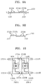
- FIG. 1 is a schematic plan view of a chip package 100 according to an embodiment of the present invention.
- FIG. 2 is a cross-sectional view of the chip package 100 of FIG. 1 taken along a line A-A'.
- the chip package 100 includes a light-emitting device chip 140, a lead frame 110 for electrically connecting the light-emitting device chip 140 to an external device, and a reflective cavity 150 for reflecting light emitted from the light-emitting device chip 140 to guide the light outwards.
- the lead frame 110 may be formed of a conductive metal such as aluminum (Al), or copper (Cu) by using a press process, an etching process, or the like.
- the lead frame 110 includes a first frame portion 120 and a second frame portion 130 that are separately formed from each other.
- the first frame portion 120 and the second frame portion 130 are fixed to each other by the reflective cavity 150 formed of an insulating resin.
- the first frame portion 120 includes a first connection portion 121, a first front terminal 122, and a first rear terminal 123.
- the first connection portion 121 is connected to a negative (-) electrode of the light-emitting device chip 140.
- the first front terminal 122 extends from the first connection portion 121 towards a front end of the chip package 100
- the first rear terminal 123 extends from the first connection portion 121 towards a rear end of the chip package 100.
- the second frame portion 130 includes a second connection portion 131, a second front end terminal 132, and a second rear terminal 133.
- the second connection portion 131 is connected to a positive (+) electrode of the light-emitting device chip 140.
- the second front end terminal 132 extends from the second connection portion 131 towards the front end of the chip package 100, and the second rear terminal 133 extends from the second connection portion 131 towards the rear end of the chip package 100.
- the first connection portion 121 and the second connection portion 131 are spaced apart from each other by a predetermined gap (G).
- the second connection portion 131 includes a mounting portion 139 for mounting the light-emitting device chip 140 thereon.
- the chip package 100 is a chip on lead-frame type package in which the light-emitting device chip 140 is mounted directly on the mounting portion 139 of the lead frame 110.
- a bonding pad (not shown) for facilitating bonding of a plurality of light-emitting device chips 140 may be attached to the mounting portion 139. If necessary, the mounting portion 139 may be formed on the first connection portion 121.
- the first front terminal 122 and the second front end terminal 132 are formed at the front end of the chip package 100, and function as a negative (-) terminal and a positive (+) terminal, respectively.
- the first rear terminal 123 and the second rear terminal 133 are formed at the rear end of the chip package 100, and function as a negative (-) terminal and a positive (+) terminal, respectively.
- the first and second front terminals 122 and 132, and the first and second rear terminals 123 and 133 constitute an end portion of the chip package 100.
- the first frame portion 120 is connected to the negative (-) electrode
- the second frame portion 130 is connected to the positive (+) electrode.
- the positive (+) electrode and the negative (-) electrode may vary according to a wiring direction of the light-emitting device chip 140.
- Each of the first front terminal 122 and the second front end terminal 132 includes a first coupling portion, and each of the first rear terminal 123 and the second rear terminal 133 includes a second coupling portion.
- the first coupling portion and the second coupling portion have concave and convex shapes so as to be coupled to each other. That is, each of the first front terminal 122 and the second front end terminal 132 includes the first coupling portion having a concave rectangular shape, and each of the first rear terminal 123 and the second rear terminal 133 includes the second coupling portion having a convex rectangular shape.
- the light-emitting device chip 140 may be a light-emitting diode (LED) chip that includes two electrodes, which are the positive (+) and negative (-) electrodes, as devices.
- the LED chip may emit blue light, green light, red light, or the like, according to a material used to form the LED chip. Furthermore, the LED chip may emit light beams with various colors, such as white light, or the like, by coating phosphors on a surface of the LED chip.
- a blue LED chip may include a plurality of quantum-well active layers that are formed by alternately forming GaN and InGaN.
- a P-type clad layer and an N-type clad layer may be formed on or below the quantum-well active layers, and may be formed of a compound semiconductor such as Al X Ga Y N Z .
- An LED chip disclosed in Korean Application No. 2010-015422 or 2010-018259 may be used as the light-emitting device chip 140.
- the light-emitting device chip 140 is an LED chip, but is not limited thereto.
- the light-emitting device chip 140 may be an ultraviolet (UV) ray diode chip, a laser diode chip, an organic light emitting diode (OLED) chip, or the like.
- UV ultraviolet
- OLED organic light emitting diode
- the reflective cavity 150 is formed on the first connection portion 121 and the second connection portion 131 so as to surround the light-emitting device chip 140. Light emitted from the light-emitting device chip 140 is reflected off a reflective surface 150a so as be emitted out of the light-emitting device chip 140 within a predetermined range of a reflection angle, thereby improving an efficiency of extracting the light, which was emitted from the light-emitting device chip 140, outwards.
- the reflective cavity 150 may be formed of an insulating resin such as an epoxy resin, a silicon resin, plastic, or the like by using an injection molding method.
- the light-emitting device chip 140 may be installed in a space surrounded by the reflective cavity 150, and then the space may be filled with a transmissive resin 160 in order to protect the light-emitting device chip 140.
- the transmissive resin 160 includes a phosphor so as to emit predetermined fluorescence.
- the transmissive resin 160 includes blue, red and green phosphor powders, thereby realizing white light.
- the phosphor may be an oxide-based phosphor, a nitride-based phosphor, a sulfide-based phosphor, a silicate-based phosphor, a phosphate-based phosphor, a selenide-based phosphor, or a phosphor using a quantum dot.
- a greenish phosphor may be a YAG-based phosphor
- a green phosphor may be a nitride-based phosphor such as Ca A Al B O C N D
- a green phosphor may be a silcide-based phosphor such as (Ba,Sr) X Si Y O Z .
- the reflective cavity 150 is formed on the first connection portion 121 and the second connection portion 131, the first connection portion 121 and the second connection portion 131 are fixed to each other by the reflective cavity 150.
- An insulating material may be coated to form an insulating layer (not shown) on the lead frame 110 except for a portion for electrical connection of the light-emitting device chip 140 or terminals.
- the insulating layer may be formed of the same material as the reflective cavity 150, and may be simultaneously formed with the reflective cavity 150.
- FIG. 3 is a plan view of a package module in which a first chip package 100A and a second chip package 100B are connected in parallel to each other, according to an embodiment of the present invention.
- FIG. 4 is a circuit diagram of the package module of FIG. 3 .
- the package module according to the present embodiment includes the first chip package 100A and the second chip package 100B.
- the first chip package 100A and the second chip package 100B are instrumentally and electrically connected to each other.
- Each of the first chip package 100A and the second chip package 100B corresponds to the chip package 100 described with reference to FIGS. 1 and 2 .
- the first chip package 100A and the second chip package 100B may be directly connected to each other. That is, a second convex coupling portion of a first rear terminal 123A of the first chip package 100A is coupled to a first concave coupling portion of a first front terminal 123B of the second chip package 100B, and a second convex coupling portion of a second rear terminal 133A of the first chip package 100A is coupled to a first concave portion of a second front terminal 133B of the second chip package 100B.
- the first chip package 100A and the second chip package 100B are instrumentally and electrically connected to each other.
- a negative (-) electrode of a light-emitting device chip 140A of the first chip package 100A is connected to a negative (-) electrode of a light-emitting device chip 140B of the second chip package 100B
- a positive (+) electrode of the light-emitting device chip 140A of the first chip package 100A is connected to a positive (+) electrode of the light-emitting device chip 140B of the second chip package 100B.
- the package module according to the present embodiment may include a structure in which the first chip package 100A and the second chip package 100B are connected in parallel to each other, as shown in FIG. 4 .
- the chip packages 100A and 100B may be directly connected without mounting the chip packages 100A and 100B on a separate substrate or soldering the chip packages 100A and 100B together.
- terminals of front and rear ends of the package module, which are exposed out of the package module may be coupled to a socket, or various connectors, and thus the package module may be directly used as an illumination module of an illumination apparatus.
- FIGS. 5A and 5B are plan views for explaining modified examples of the first and second coupling portions of the chip package 100 of FIG. 1 , according to embodiments of the present invention.
- Chip packages 100' and 100" of FIGS. 5A and 5B are each the same as the chip package 100 except for a coupling structure formed on each terminal.
- the chip package 100' includes a first front terminal 122' and a second front terminal 132' which each include a second convex coupling portion and a first concave coupling portion, and a first rear terminal 123' and a second rear terminal 133' which each include a first concave coupling portion and a second convex coupling portion.
- the chip package 100' is different from the chip package 100 described with reference to FIGS.
- the chip package 100 includes the first front terminal 122 and the second front end terminal 132 which include coupling structures having the same shape (i.e., the first coupling portion), and the first rear terminal 123 and the second rear terminal 133 which include coupling structures having the same shape (i.e., the second coupling portion). Since the chip package 100' includes the first concave coupling portion and the second convex coupling portion which are formed at front and rear ends of the chip package 100', and have complementary shapes, a front end and a rear end of the chip package 100' may also be coupled to a front end and a rear end of another chip package 100', respectively (see FIG. 23 ).
- the chip package 100" includes a first front terminal 122" and a second front terminal 132" which each include a first concave coupling portion having an inverted triangular shape, and a first rear terminal 123" and a second rear terminal 133" which each include a second convex coupling portion having an inverted triangular shape.
- the chip package 100" is different from the chip package 100 described with reference to FIGS. 1 and 2 in that the first coupling portion of the chip package 100 has a concave rectangular shape, and the second coupling portion of the chip package 100 has a convex rectangular shape.
- first coupling portion and the second coupling portion have concave and convex inverted-triangular shapes, respectively, but may have various complementary shapes.
- the light-emitting device chip 140 is bonded to the lead frame 110 by using a wire-bonding method within the reflective cavity 150, but the present embodiment is not limited thereto.
- FIGS. 6A through 6D are cross-sectional of modified examples of mounting a light-emitting device chip 140 according to embodiments of the present invention.
- a lens 170 may be disposed on the reflective cavity 150 for accommodating the light-emitting device chip 140 therein.
- the lens 170 may condense or diverge light emitted from the light-emitting device chip 140 so as to appropriately distribute the light.
- the lens 170 may be formed of a transparent resin or glass.
- the lens 170 may be formed directly on the reflective cavity 150, or alternatively, may be previously formed, and then may be attached onto the reflective cavity 150.
- the transmissive resin 160 and the lens 170 may be formed integrally with each other.
- a chip package of FIG. 6A is the same as the chip package 100 of FIG. 1 except for the lens 170, and thus, a description thereof will not be repeated here.
- the reflective cavity 150 may be omitted.
- a transmissive resin 161 is coated on the light-emitting device chip 140 that is bonded to the lead frame 110 by using a wire-bonding method without a reflective capacity.
- the transmissive resin 161 may emit white light or fluorescence.
- a plurality of layers formed of the transmissive resin 161 including the phosphors may be coated on the light-emitting device chip 140.
- a first layer of the transmissive resin 161 may include a red phosphor
- a second layer of the transmissive resin 161 may include a green phosphor.
- a lens 171 is disposed on the transmissive resin 161 so as to condense or diverge light emitted from the light-emitting device chip 140.
- the transmissive resin 161 and the lens 171 may be formed integrally with each other.
- the light-emitting device chip 140' is bonded to the lead frame 110 by using a flip-chip bonding method.
- the light-emitting device chip 140' is electrically connected to the lead frame 110 by bumps 45 and 46 formed of a conductive material such as gold (Au).
- Au gold
- the flip-chip bonding method When the flip-chip bonding method is used, light is emitted from a surface of the light-emitting device chip 140' that is opposite to a surface bonded to the lead frame 110.
- a transmissive resin 162 may be coated on the light-emitting device chip 140' that is bonded to the lead frame 100 by using the flip-chip bonding method.
- a phosphor may be sprayed on the transmissive resin 162.
- the transmissive resin 162 may be formed in a film shape, and may cover the light-emitting device chip 140'.
- a lens 172 may be formed on the transmissive resin 162.
- the first connection portion 121 and the second connection portion 131 of the lead frame 110 may be fixed to each other by the transmissive resin 161 or 162, the lens 171 or 172, or a separate coupling member (not shown).
- a lead frame 110' includes a bent portion 110'a that defines a predetermined space.
- a heat slug 118 is disposed in the space defined by the bent portion 110'a so as to be spaced apart from the bent portion 110'a.
- the heat slug 118 is fixed to the lead frame 110' by a fixation member 119.
- the heat slug 118 is used for mounting the light-emitting device chip 140 thereon.
- the light-emitting device chip 140 is bonded to the heat slug 118, and is electrically connected to the bent portion 110'a of the lead frame 110' through wires 141 and 142.
- the heat slug 118 is formed of a metal having a high thermal conductivity so as to function as a path for dissipating heat generated from the light-emitting device chip 140.
- a transmissive resin 163 may be coated on the light-emitting device chip 140, and may include a phosphor.
- the light-emitting device chip 140 may be surrounded by a reflective cavity 150'.
- a lens 174 may be disposed above the light-emitting device chip 140.
- the heat dissipation properties of a chip package of FIG. 6D may be improved by the heat slug 118.
- various known structures for dissipating heat may be used.
- a single light-emitting device chip 140 is disposed in a space defined by the reflective cavity 150 (see FIG. 2 ), or the transmissive resin 160, 161 or 162, but a plurality of light-emitting device chips may be disposed in the space.
- an amount of light may be increased by disposing light-emitting device chips for emitting light beams with the same color in the space, or color rendering properties may be increased by disposing light-emitting device chips for light beams with different colors.
- the light-emitting device chips may be connected to each other at a wafer level, or may be bond to the lead frame 110, and then may be connected in parallel and/or series to each other by using various known methods.
- a Zener diode chip may also be mounted in order to protect the light-emitting device chip 140.
- FIG. 7 is a plan view of a modified example of the reflective cavity 150 of the chip package 100 of FIG. 1 , according to an embodiment of the present invention.
- the reflective cavity 150' is formed on the first connection portion 121 and the second connection portion 131 to extend beyond outer edges of the first connection portion 121 and the second connection portion 131. That is, since the reflective cavity 150' is formed so as to extend beyond an outer edge of the lead frame 110, the first connection portion 121 and the second connection portion 131 are fixed to each other, and the first rear terminal 123 extending from the first connection portion 121, and the second front end terminal 132 extending from the second connection portion 131 may also be fixed to each other. Furthermore, since the reflective cavity 150' is formed so as to extend beyond an edge of the lead frame 110, the insulating property of the chip package 100 may be improved. The reflective cavity 150' may be formed so as to surround the lead frame 110, or may be formed only on the lead frame 110.
- FIG. 8 is a schematic plan view of a chip package 100 according to another embodiment of the present invention.
- FIGS. 9A and 9B are schematic cross-sectional views of a first frame portion 220 and a second frame portion 230 of FIG. 8 , respectively, according to embodiments of the present invention.
- the chip package 200 is materially the same as the above-described chip package 100 except for a coupling structure formed on a lead frame 210.
- the above-described embodiments may be applied to a mounting structure of the light-emitting device chip 140 and a structure of the reflective cavity 150.
- the chip package 200 includes the light-emitting device chip 140, the lead frame 210 for electrically connecting the light-emitting device chip 140 to an external device, and the reflective cavity 150 for reflecting light emitted from the light-emitting device chip 140 to guide outwards the light.
- the lead frame 210 includes the first frame portion 220 and the second frame portion 230 that are separately formed from each other. The first frame portion 220 and the second frame portion 230 are fixed to each other by the reflective cavity 150 formed of an insulating resin.
- the first frame portion 220 includes a first connection portion 221, a first front terminal 222, and a first rear terminal 223.
- the first connection portion 221 is connected to a negative (-) electrode of the light-emitting device chip 140.
- the first front terminal 222 extends from the first connection portion 221 towards a front end of the chip package 200, and the first rear terminal 223 extends from the first connection portion 221 towards a rear end of the chip package 200.
- the second frame portion 230 includes a second connection portion 231, a second front terminal 232, and a second rear terminal 233.
- the second connection portion 231 is connected to a positive (+) electrode of the light-emitting device chip 140.
- the second front terminal 232 extends from the second connection portion 231 towards the front end of the chip package 200, and the second rear terminal 233 extends from the second connection portion 231 towards the rear end of the chip package 200.
- the first front terminal 222 and the second front terminal 232 include a first coupling portion and a second coupling portion, respectively, and the first rear terminal 223 and the second rear terminal 233 include a second coupling portion and a first coupling portion, respectively.
- the first coupling portions of the first front terminal 222 and the second rear terminal 233 include at least one protrusion 222a and at least one protrusion 233a, respectively.
- the second coupling portions of the second front terminal 232 and the first rear terminal 223 include coupling grooves 232a and 223a corresponding to the protrusions 222a and 233a, respectively.
- the protrusions 222a and 233a may be formed of an insulating layer by using an injection molding method, and may be formed simultaneously with the reflective cavity 150. Alternatively, the protrusions 222a and 233a may be formed by forming protrusions from the lead frame 210 by using a press process during a chip packaging process.
- the protrusions 222a and 233a, and the coupling grooves 232a and 223a are coupled to each other by overlapping the lead frame 210 with another lead frame 210.
- some of the first front terminal 222, the second front terminal 232, the first rear terminal 223 and the second rear terminal 233 may be bent and stepped.
- the first rear terminal 223 and the second front terminal 232 including the coupling grooves 223a and 232a may include bent portions 223b and 232b, respectively, and the bent portions 223b and 232b may each be formed to have a step 'H' therebetween.
- the step 'H' may be the same as a thickness 'T' of the lead frame 210.
- the first rear terminal 223 and the second front terminal 232 including the coupling grooves 223a and 232a are bent, but the present embodiment is not limited thereto.
- the first front terminal 222 and the second rear terminal 233 including the protrusions 222a and 233a may be bent with the step 'H'.
- the protrusions 222a and 233a, and the coupling grooves 232a and 223a are formed at front and rear ends of the chip package 200, but the present embodiment is not limited thereto.
- the protrusions 222a and 233a may be formed on the first front terminal 222 and the second front terminal 232, and only the coupling grooves 232a and 223a may be formed on the first rear terminal 223 and the second rear terminal 233.
- FIG. 10 is a plan view of a package module in which a first chip package 200A and a second chip package 200B are connected in parallel to each other, according to another embodiment of the present invention.
- FIGS. 11A and 11B are cross-sectional views for explaining a coupling structure of the package module of FIG. 10 .
- the package module according to the present embodiment includes the first chip package 200A and the second chip package 200B.
- the first chip package 200A and the second chip package 200B are instrumentally and electrically connected to each other.
- Each of the first chip package 200A and the second chip package 200B corresponds to the chip package 200 described with reference to FIGS. 8 , 9A and 9B .
- a protrusion 222Ba of a first front terminal 223B of the second chip package 200B is inserted into a coupling groove 223Aa of a first rear terminal 223A of the first chip package 200A, and a protrusion 233Aa of a second rear terminal 233A of the first chip package 200A is inserted into a coupling groove 233Aa of a second front terminal 233B of the second chip package 200B.
- the first chip package 200A and the second chip package 200B are instrumentally and electrically connected to each other. In this case, referring to FIGS.
- the first rear terminal 223A of the first chip package 200A, and the second front terminal 233B of the second chip package 200B are each formed to have a step 'H' therebetween, and thus the first chip package 200A and the second chip package 200B may be coupled to each other without distortion.
- a negative (-) electrode of the light-emitting device chip 140A of the first chip package 200A is connected to a negative (-) electrode of the light-emitting device chip 140B of the second chip package 200B, and a positive (+) electrode of the light-emitting device chip 140A of the first chip package 200A is connected to a positive (+) electrode of the light-emitting device chip 140B of the second chip package 200B.
- the package module has a structure in which the first chip package 200A and the second chip package 200B are connected in parallel to each other.
- FIG. 12 is a schematic plan view of a chip package 300 according to another embodiment of the present invention.
- FIG. 13 is a circuit diagram of the chip package 300 of FIG. 12 .
- the chip package 300 includes a plurality of light-emitting device chips 140, a lead frame 310 for electrically connecting the light-emitting device chips 140 to an external device, coupling members 350 for fixing portions of the lead frame 310, and the reflective cavity 150 for reflecting light emitted from the light-emitting device chips 140 to guide the light outwards.
- the lead frame 310 includes a first frame portion 320, a second frame portion 330, and intermediate connection portions 340 that are separately formed from each other.
- the first frame portion 320, the second frame portion 330, and the intermediate connection portions 340 are fixed by the coupling members 350 formed of an insulating resin, and the reflective cavity 150.
- the first frame portion 320 includes a first connection portion 321, a first front terminal 322, a first rear terminal 323, and a first extension portion 324.
- the first connection portion 321 is connected to a negative (-) electrode of the foremost light-emitting device chip 140 of the light-emitting device chips 140 that are arranged in a line.
- the first front terminal 322 extends the first connection portion 321 towards a front end of the chip package 300, and the first rear terminal 323 extends from the first connection portion 321 towards a rear end of the chip package 300.
- the first extension portion 324 connecting the first connection portion 321 and the first rear terminal 323 to each other is spaced apart from the intermediate connection portions 340 by a predetermined distance along one side of an arrangement line of the light-emitting device chips 140.
- the second frame portion 330 includes a second connection portion 331, a second front terminal 332, a second rear terminal 333, and a second extension portion 334.
- the second connection portion 331 is connected to a positive (+) electrode of the rearmost light-emitting device chip 140 of the light-emitting device chips 140 that are arranged in a line.
- the second front terminal 332 extends from the second connection portion 331 towards the front end of the chip package 300, and the second rear terminal 333 extends from the second connection portion 331 to the rear end of the chip package 300.
- the second extension portion 334 connecting the second connection portion 331 and the second front terminal 332 to each other is spaced apart from the intermediate connection portions 340 by a predetermined distance along the other one side of the arrangement line of the light-emitting device chips 140.
- the first front terminal 322 and the second front terminal 332 are formed at the front end of the chip package 300, and function as a negative (-) terminal and a positive (+) terminal, respectively.
- the first rear terminal 323 and the second rear terminal 333 are formed at the rear end of the chip package 300, and function as a negative (-) terminal and a positive (+) terminal, respectively.
- the first and second front terminals 322 and 332, and the first and second rear terminals 323 and 333 constitute an end portion of the chip package 300.
- Each of the first front terminal 122 and the second front end terminal 132 includes a first coupling portion
- each of the first rear terminal 123 and the second rear terminal 133 includes a second coupling portion.
- the first coupling portion and the second coupling portion have concave and convex shapes so as to be coupled to each other.
- the intermediate connection portions 340 is disposed between the first connection portion 321 and the second connection portion 331.
- the light-emitting device chips 140 are arranged in a line, and thus the first connection portion 321, the intermediate connection portions 340, and the second connection portion 331 are also arranged in a line.
- an overall shape of the chip package 300 may be a bar shape.
- the intermediate connection portions 340 are disposed between the light-emitting device chips 140 so as to connect positive (+) and negative (-) electrodes of the light-emitting device chips 140to each other. There is one less intermediate connection portion 340 than light-emitting device chips 140. For example, as shown in FIG. 12 , when the number of the light-emitting device chips 140 is six, the number of the intermediate connection portions 340 is five.
- the intermediate connection portions 340 together with the first connection portion 321 and the second connection portion 331 are used to connect the light-emitting device chips 140 in series to each other.
- the light-emitting device chips 140 may be indicated by a circuit diagram of FIG. 13 .
- the light-emitting device chips 140 may emit light beams with a single color or different colors.
- the light-emitting device chips 140 may be blue LED chips, or color rendering properties may be increased by using blue and red LED chips.
- a Zener diode chip (not shown) may also be mounted in order to protect the light-emitting device chips 140. In this case, the Zener diode chip may be mounted on every light-emitting device chip 140 or may be selectively mounted on some of the light-emitting device chips 140.
- a plurality of light-emitting device chips 140 or a single light-emitting device chip 140 may be installed in a single reflective cavity 150.
- the plurality of the light-emitting device chips 140 When the plurality of the light-emitting device chips 140 are installed in the single reflective cavity 150, the plurality of the light-emitting device chips 140 may be connected to each other in a wafer level, or may be bonded to the lead frame 310 and then may be connected in parallel and/or series to each other by using various known methods.
- the number of the light-emitting device chips 140 is six, but the present embodiment is not limited thereto.
- the number of the light-emitting device chips 140 may be appropriately determined according to the power of an illumination apparatus using the chip package 300.
- the lead frame 310 since the lead frame 310 has repeated patterns formed along an arrangement line of the light-emitting device chips 140, the number of the intermediate connection portions 340 may be easily changed according to the required number of the light-emitting device chips 140.
- FIG. 14 is a plan view of a package module in which a first chip package 300A and a second chip package 300B are connected in parallel to each other, according to another embodiment of the present invention.
- FIG. 15 is a circuit diagram of the package module of FIG. 14 .
- the package module according to the present embodiment includes a first chip package 300A and a second chip package 300B.
- the first chip package 300A and the second chip package 300B are instrumentally and electrically connected to each other.
- Each of the first chip package 300A and the second chip package 300B corresponds to the chip package 300 described with reference to FIGS. 12 and 13 .
- first chip package 300A and the second chip package 300B include coupling portions formed on respective terminals, the first chip package 300A and the second chip package 300B may be directly connected to each other.
- a first rear terminal 323A of the first chip package 300A is coupled to a first front terminal 323B of the second chip package 300B
- a second rear terminal 333A of the first chip package 300A is coupled to a second front terminal 333B of the second chip package 300B.
- the first chip package 300A and the second chip package 300B are instrumentally and electrically connected to each other.
- the first rear terminal 323A of the first chip package 300A, and the first front terminal 323B of the second chip package 300B may each function as a negative (-) terminal
- the second rear terminal 333A of the first chip package 300A and the second front terminal 333B of the second chip package 300B may each function as a positive (+) electrode.
- the package module according to the present embodiment has a structure in which the first chip package 300A and the second chip package 300B are connected in parallel to each other, as shown in FIG. 15 .
- the package module includes the first and second chip packages 300A and 300B that are connected.
- three or more chip packages may be consecutively connected so as to embody a line source that extends in a longitudinal direction.
- FIG. 16 is a schematic plan view of a chip package 300' according to another embodiment of the present invention.
- FIG. 17 is a schematic plan view of a package module in which chip packages are connected in series to each other, according to another embodiment of the present invention.
- FIG. 18 is a circuit diagram of the package module of FIG. 17 .
- the chip package 300' is configured by adding a separate coupling structure to the chip package 300 described with reference to FIG. 12 .
- the chip package 300' further includes a third coupling portion 325 formed at an edge of the first extension portion 324 of a first frame portion 320', and a fourth coupling portion 335 formed at an edge of the second extension portion 334 of a second frame portion 330'.
- the third coupling portion 325 and the fourth coupling portion 335 have complementary shapes so as to be coupled to each other.
- the third coupling portion 325 and the fourth coupling portion 335 may have a square concave shape and a square convex shape, or various complementary shapes.
- a first chip package 300'A and a second chip package 300'B are connected perpendicularly to a longitudinal direction of the bar-shaped lead frame 310', as shown in FIG. 17 .
- the package module includes the first chip package 300'A and the second chip package 300'B.
- a third coupling portion 325A formed on a first extension portion 324A is coupled to a fourth coupling portion 325B formed on a second extension portion 324B of the second chip package 300'B, and thus the light-emitting device chips 140A and 140B may be arranged in a matrix so as to function as a surface illumination apparatus.
- a first extension portion 324 of the first chip package 300'A is electrically connected to the second extension portion 324B of the second chip package 300'B, and thus the first chip package 300'A and the second chip package 300'B are connected in series to each other, as shown in FIG. 18 .
- the package module includes the first and second chip packages 300'A and 300'B that are connected in a longitudinal direction.
- three or more chip packages may be consecutively connected. In this case, some terminals of the chip packages, which contact each other, may be short-circuited, if necessary.
- FIG. 19 is a schematic plan view of a chip package 400 according to another embodiment of the present invention.
- FIG. 20 is a circuit diagram of the chip package 400 of FIG. 19 .
- the chip package 400 is formed by arranging the light-emitting device chips 140 in parallel to each other. Referring to FIGS. 19 and 20 , the chip package 400 includes a lead frame 410, the light-emitting device chips 140, and the reflective cavity 150.
- the lead frame 410 includes a first frame portion 420 and a second frame portion 430, and has a long bar shape. Two ends of the first frame portion 420 extend to form a first front terminal 422 and a first rear terminal 423, and two ends of the second frame portion 430 extend to form a second front terminal 432 and a second rear terminal 433.
- first front terminal 422 and the second front terminal 432 include a second convex coupling portion and a first concave coupling portion, respectively, and the first rear terminal 423 and the second rear terminal 433 include a first concave coupling portion and a second convex coupling portion.
- the first frame portion 420 and the second frame portion 430 are spaced apart from each other by a predetermined distance, and any one of the first frame portion 420 and the second frame portion 430 includes a plurality of mounting portions (refer to the mounting portions 139 of FIG. 2 ).
- the light-emitting device chips 140 are mounted on the mounting portions, and electrical arrangement of the light-emitting device chips 140 is performed by using various known bonding methods such as a wire-bonding or flip-chip bonding method.
- Positive (+) electrodes of the light-emitting device chips 140 are commonly and electrically connected to the first frame portion 420, and negative (-) electrodes of the light-emitting device chips 140 are commonly and electrically connected to the second frame portion 430.
- the light-emitting device chips 140 are connected in parallel to each other by the first frame portion 420 and the second frame portion 430.
- FIG. 21 illustrates a package module in which a first chip package 400A and a second chip package 400B are connected in parallel to each other, according to another embodiment of the present invention.
- FIG. 22 is a circuit diagram of the package module of FIG. 21 .
- the package module includes the first chip package 400A and the second chip package 400B.
- the first chip package 400A and the second chip package 400B are instrumentally and electrically connected to each other.
- Each of the first chip package 400A and the second chip package 400B corresponds to the chip package 400 described with reference to FIGS. 19 and 20 .
- a first rear terminal 423A of the first chip package 400A is coupled to a first front terminal 423B of the second chip package 400B
- a second rear terminal 433A of the first chip package 400A is coupled to a second front terminal 433B of the second chip package 400B.
- the first chip package 400A and the second chip package 400B are instrumentally and electrically connected to each other.
- the first rear terminal 423A of the first chip package 400A and the first front terminal 423B of the second chip package 400B may each function as a negative (-) electrode
- the second rear terminal 433A of the first chip package 400A and the second front terminal 433B of the second chip package 400B may each function as a positive (+) electrode.
- the package module according to the present embodiment includes a structure in which the first chip package 400A and the second chip package 400B are connected in parallel to each other, as shown in FIG. 22 .
- FIG. 23 is a plan view of a package module in which the first chip package 400A and the second chip package 400B are connected in series to each other, according to another embodiment of the present invention.
- FIG. 24 is a circuit diagram of the package module of FIG. 23 .
- the package module includes the first chip package 400A and the second chip package 400B.
- Each of the first chip package 400A and the second chip package 400B corresponds to the chip package 400 described with reference to FIGS. 19 and 20 .
- the first rear terminal 423A of the first chip package 400A is coupled to a second rear terminal 433B of the second chip package 400B, and thus the first chip package 400A and the second chip package 400B are instrumentally and electrically connected to each other.
- at least one of the second rear terminal 433A of the first chip package 400A and a first rear terminal 422B of the second chip package 400B may be bent or removed so as to be short-circuited.
- the first rear terminal 423A of the first chip package 400A is connected to negative (-) electrodes of the light-emitting device chips 140A, but the second rear terminal 433B of the second chip package 400B is connected to positive (+) electrodes of the light-emitting device chips 140B.
- the light-emitting device chips 140A of the first chip package 400A and the light-emitting device chips 140B of the second chip package 400B are connected in series to each other.
- FIG. 25 is a structural diagram of a package module in which chip packages are connected in a combination of parallel and series to each other, according to another embodiment of the present invention.
- FIG. 26 is a circuit diagram of the package module of FIG. 25 .
- the package module according to the present embodiment includes chip packages 400A, 400B, 400C, 400D, 400E and 400F that are connected in a combination of parallel (see FIG. 21 ) and series (see FIG. 23 ).
- the chip packages 400A, 400B, 400C, 400D, 400E and 400F are obtained by connecting six light-emitting device chips 140 in parallel to each other, each pair of the chip packages (400A and 400B), (400C and 400D), and (400E and 400F) may be connected in parallel, as shown in FIG. 21 , and the chip packages (400A and 400B), (400C and 400D), and (400E and 400F) may be connected in series to each other, as shown in FIG. 23 .
- the number of the chip packages may be a multiple of six.
- FIG. 27 is a schematic plan view of a chip package 400' according to another embodiment of the present invention.
- FIG. 28 is a plan view of a package module in which a first chip package 400'A and a second chip package 400'B are connected in series to each other, according to another embodiment of the present invention.
- FIG. 29 is a circuit diagram of the package module of FIG. 28 .
- the chip package 400' is formed by adding a separate coupling structure to the chip package 400 described with reference to FIG. 19 .
- the chip package 400' further includes a third coupling portion 424 formed at an edge of a first connection portion 421 of a first frame portion 420', and a fourth coupling portion 434 formed at an edge of a second connection portion 431 of a second frame portion 430'.
- the third coupling portion 424 and the fourth coupling portion 434 have complementary shapes so as to be coupled to each other.
- the third coupling portion 424 and the fourth coupling portion 434 may have a square concave shape and a square convex shape, or various complementary shapes.
- the chip package 400' are connected perpendicularly to a longitudinal direction of the bar-shaped lead frame 410', as shown in FIG. 28 .
- the package module includes a first chip package 400'A and a second chip package 400'B.
- a third coupling portion 424A formed on a first connection portion 421A of the first chip package 400'A is coupled to a fourth coupling portion 434B formed on a second connection portion 431 B of the second chip package 400'B, and thus the light-emitting device chips 140A and 140B may be arranged in a matrix so as to function as a surface illumination apparatus.
- the first connection portion 421A of the first chip package 400'A is electrically connected to a second connection portion 431 B of the second chip package 400'B, and thus the first chip package 400'A and the second chip package 400'B are connected in series to each other, as shown in FIG. 29 .
- FIGS. 30A through 30G are diagrams for explaining a method of manufacturing the chip package 300, according to an embodiment of the present invention.
- FIGS. 31A through 31C illustrate the lead frame 310 on a sheet-by-sheet basis, during the manufacture of the chip package 300.
- the chip package 300 shown in FIGS. 30A through 30G and 31A through 31C corresponds to the chip package 300 described with reference to FIG. 12 .
- FIG. 30A is a plan view of the lead frame 310.
- FIG. 30B is a cross-sectional view of the lead frame 310.
- a material or thickness of the lead frame 310 may be known to one of ordinary skill in the art.
- the lead frame 310 may be formed of metal such as aluminum (Al), or copper (Cu) with a sub-millimeter thickness, and may have a pattern formed by using a press process, an etching process, or the like.
- the lead frame 310 is supported by the first frame portion 320, and the second frame portion 330.
- the intermediate connection portions 340 are connected and supported by cleavage portions 317.
- the first front terminal 322 and the first rear terminal 323 that are respectively formed on ends of the first frame portion 320 include coupling structures having complementary shapes, respectively, as shown in FIG. 30A .
- the second front terminal 332 and the second rear terminal 333 that are respectively formed on ends of the second frame portion 330 include coupling structures having complementary shapes, respectively, as shown in FIG. 30A .
- the lead frame 310 is included in a single chip package.
- a single lead frame 310 may have a plurality of patterns, as shown in FIG. 31A .
- the coupling structure having complementary shapes of ends of the lead frame 310 may be simultaneously formed when the patterns of the lead frame 310 are formed.
- the reflective cavity 150 is formed on the lead frame 310.
- the reflective cavity 150 may be formed of an epoxy resin, a silicon resin, plastic, or the like by using an injection molding method. If the coupling structure having complementary shapes of the ends of the lead frame 310 is a protrusion and coupling groove set, the protrusion may be simultaneously formed when the reflective cavity 150 is formed by using an injection molding method.
- the coupling members 350 for fixing the first frame portion 320 and the intermediate connection portions 340, and the second frame portion 330 and the intermediate connection portions 340 to each other may be simultaneously formed. If necessary, as shown in FIG. 7 , the reflective cavity 150 may extend, and the coupling members 350 may be omitted.
- the reflective cavity 150 and the coupling members 350 may be formed on a sheet-by-sheet basis of the lead frame 310, as shown in FIG. 31B .
- the light-emitting device chips 140 are mounted on the lead frame 310.
- the light-emitting device chips 140 may be formed on the mounting portion 139 (see FIG. 2 ) by using a die attaching method.
- wires are used to electrically arrange the light-emitting device chips 140, and a transparent resin is filled inside the reflective cavity 150. If necessary, a lens may be added.
- FIG. 30G shows the cleavage portions 317 of the lead frame 310 when the cleavage portions 317 are removed.
- the cleavage portions 317 of the chip package 300 may be immediately removed.
- the light-emitting device chips 140 are electrically connected.
- the light-emitting device chips 140 are powered on, electric arrangement states or light-emitting states of the light-emitting device chips 140 may be tested.
- the chip packages 300 may be attached to each other in the lead frames 310 by using known methods (e.g., a tie bar).
- FIG. 32 is a structural diagram of an illumination apparatus 500 including a chip package, according to an embodiment of the present invention.
- the illumination apparatus 500 includes an illumination module 590, and a power supplying unit 510 for supplying power to the illumination module 590.
- the illumination module 590 may use the chip packages or the package module, described with reference to FIGS. 1 through 15 .
- the power supplying unit 510 may include an interface 520 for receiving power, and a power controller 530 for controlling the power supplied to the illumination module 590.
- the interface 520 may include a fuse for shutting-off an excess current, and an electromagnetic wave shielding filter for preventing electromagnetic interference.
- the power may be supplied from an external source, or a battery included in the illumination apparatus 500.
- the power controller 530 may further a rectifying portion for converting alternative current (AC) to direct current (DC), and a static voltage controller for converting a voltage to a voltage that is appropriate to the illumination module 590.
- a power source is a DC source (e.g., a battery) having an appropriate voltage to the illumination module 590
- the rectifying portion or the static controller may be omitted.
- AC-LED when used as a light-emitting device chip of the illumination module 590, AC power may be supplied directly to the illumination module 590.
- the rectifying portion or the static controller may also be omitted.
- the illumination module 590 controls a color temperature, or the like so as to realize illumination according to a user's emotion.
- Various types of the illumination apparatus 500 may be used by using a light source.
- a package module including chip packages that are connected in a longitudinal direction may be used as a linear light source.
- the package modules are connected in parallel to each other in a longitudinal direction so as to embody a surface illumination apparatus, or the chip packages may be connected in longitudinal and width directions so as to embody a surface illumination apparatus.
- the illumination apparatus 500 may be a general illumination apparatus replacing a general electric bulb or fluorescent lamp, an illumination apparatus used in a vehicle, a vessel or an aircraft, or an illumination apparatus for emitting light with a predetermined wavelength, used in a home appliance product such as a refrigerator, a television, a washer, etc.
- a general illumination apparatus replacing a general electric bulb or fluorescent lamp a plurality of light-emitting device chips are included in a single chip package, and thus an amount of light may be increased.
- color rendering properties may be increased by disposing light-emitting device chips such as a blue light-emitting device chip and a red light-emitting device chip.
- a phosphor is used in a light-emitting device chip to emit blue, red and green light beams, and thus an emotionally compatible apparatus may be realized so as to realize colors that are appropriate for indoor and outdoor environments.
- the illumination apparatus 500 may be a non-self light-emitting display panel such as a liquid crystal display (LCD) panel, or a backlight unit of a large-scaled billboard.
- a non-self light-emitting display panel such as a liquid crystal display (LCD) panel, or a backlight unit of a large-scaled billboard.
- LCD liquid crystal display
- an etch-type backlight unit is configured by a linear light source at a side of a guiding plate, and thus the linear light source used in the etch-type backlight unit may be used in a package module in which chip packages are connected in a longitudinal direction, as described in the previous embodiments.
- a direct-light type backlight unit uses a surface light source.
- a package module in which chip packages are connected in parallel to each other in a longitudinal direction may function as a surface light source.
- a package module in which chip packages are connected in longitudinal and width directions may be used a surface light source.
- these package modules are arranged so as to function as a surface light source.
- the illumination module 590 uses a plurality of light-emitting device chips in order to ensure a sufficient amount of light.
- primary packaging is performed on light-emitting device chips (e.g., LED chips) together with a phosphor and a lens on a lead frame.
- the light-emitting device chips on which the primary packaging is performed are connected in parallel and/or in series, and secondary packaging is performed so that the light-emitting device chips are mounted on a printed circuit board (PCB).
- PCB printed circuit board
- the illumination apparatus 500 uses a chip package in which a plurality of light-emitting device chips are connected in parallel and/or in series on a lead frame, and packaging is performed.
- chip packages may be coupled directed to each other according to capacity of the illumination apparatus 500 or a space for installing the illumination apparatus 500, and may be immediately used as an illumination module.
- the illumination apparatus 500 immediately constitutes a circuit of light-emitting device chips during a packaging operation, and simultaneously, chip packages are simply coupled to each other, thereby simplifying a packaging operation and reducing manufacturing costs.
- a general chip apart from a light-emitting chip device including two electrode structures includes at least two coupling portions that are formed on ends of a lead frame and are coupled to each other, and thus a plurality of chip packages are electrically and instrumentally connected.
- a structure of a lead frame is improved, and chip packages are connected directly to each other to constitute a module, thereby reducing manufacturing costs.
Description
- The present disclosure relates to chip packages, package modules, and illumination apparatuses including the package modules, which are used for packaging a plurality of chips.
- In general, with regard to chips, a primary packaging process is performed on chips in order to protect the chips and to easily electronically arrange the chips, and then a secondary packaging process is performed in order to mount the chips on a circuit board on which a circuit is formed by the chips together with other components. Thus, since a multistep packaging process is required to use chips in electronic devices, manufacturing costs may be increased.
- For example, in order to use light-emitting device chips such as light-emitting diode (LED) chips in illumination apparatuses, a primary packaging process is performed in order to dispose phosphors and lenses on a lead frame, and then a secondary packaging process is performed in order to mount a plurality of light-emitting device chips on a circuit board on which a circuit is formed by these chips together with other components. A LED chip is a semiconductor device for emitting light having various colors by configuring a light source formed by a PN junction of a compound semiconductor, has a long lifetime, can be miniaturized and lightweight, and can be driven at a low voltage due to strong directivity of light generated from the LED. However, in order to use a light-emitting device chip such as the LED chip as an illustration device and to replace a general inexpensive illumination apparatus with the LED chips, manufacturing costs of the LED chips need to be reduced. Thus, a significant amount of research has been conducted into a method of reducing material costs and simplifying manufacturing processes.
-
US2007/0267637 describes a light emitting device package which can be connected to another similar light emitting package with a protruding electrode mating with an electrode groove of another package. -
US2010/0072507 teaches a light emitting diode module with a lead frame and a plurality of LEDs. -
JP2003-168305 - Provided are lead frames for chip packages, chip packages, package modules, and illumination apparatuses, in which structures of chip packages are improved to simplify a packaging process and to easily arrange a circuit of the chip packages.
- Additional aspects will be set forth in part in the description which follows and, in part, will be apparent from the description, or may be learned by practice of the presented embodiments.
- According to an aspect of the present invention, there is provided a chip package according to
claim 1. - The first coupling portion and the second coupling portion may include a protrusion, and a coupling groove into which the protrusion is inserted, respectively.
- The lead frame may further include a plurality of mounting portions so as to mount a plurality of chips thereon.
- The lead frame may further include a plurality of connection portions for electrically connecting the plurality of chips.
- Each of the plurality of connection portions may include at least one intermediate connection portion for connecting the chips in series to each other; a first connection portion that is electrically connected to a first electrode of a foremost chip of the plurality of chips; and a second connection portion that is electrically connected to a second electrode of a rearmost chip of the plurality of chips, wherein the terminal portion may include a first terminal that extends from the first connection portion, and a second terminal that extends from the second connection portion.
- The first connection portion, the intermediate portion, and the second connection portion may be arranged in a line, wherein the first terminal may include a first front terminal that is disposed at a front side of the plurality of connection portions, and a first rear terminal that is disposed at a rear side of the plurality of connection portions, and wherein the second terminal may include a second front terminal that is disposed at a front side of the plurality of connection portions, and a second rear terminal that is disposed at a rear side of the plurality of connection portions.
- The first front terminal and the first rear terminal may include a first shape terminal and a second shape terminal, respectively, and the second front terminal and the second rear terminal may include a first shape terminal and a second shape terminal, respectively.
- The first front terminal and the first rear terminal may include a first shape terminal and a second shape terminal, respectively, and the second front terminal and the second rear terminal may include a second shape terminal and a first shape terminal, respectively.
- Each of the plurality of connection portions may include a first connection portion for electrically connecting first electrodes of the plurality of chips, and a second connection portion for electrically connecting second electrodes of the plurality of chips so that the plurality of chips are connected in parallel to each other.
- The first coupling portion and the second coupling portion may include a protrusion, and a coupling groove into which the protrusion is inserted, respectively.
- Any one of the first shape terminal and the second shape terminal may be stepped by a thickness of the lead frame.
- The chip may include a plurality of light-emitting device chips, wherein the chip package may further include a plurality of mounting portions so as to mount a plurality of chips thereon, and wherein the lead frame may include a plurality of connection portions for electrically connecting the plurality of light-emitting device chips.
- Each of the plurality of connection portions may include at least one intermediate connection portion for connecting the light-emitting device chips in series to each other; a first connection portion that is electrically connected to a first electrode of a foremost chip of the plurality of light-emitting device chips; and a second connection portion that is electrically connected to a second electrode of a rearmost chip of the plurality of light-emitting device chips, wherein the terminal portion may include a first terminal that extends from the first connection portion, and a second terminal that extends from the second connection portion.
- The plurality of light-emitting device chips may be arranged in a line. In this case, the first terminal may include a first front terminal that is disposed at a front side of the plurality of connection portions, and a first rear terminal that is disposed at a rear side of the plurality of connection portions, wherein the second terminal may include a second front terminal that is disposed at a front side of the plurality of connection portions, and a second rear terminal that is disposed at a rear side of the plurality of connection portions, and wherein the connection portion may include a first extension portion that extends from the first connection portion to the first rear terminal along one side of an arrangement line of the plurality of light-emitting device chips, and a second extension portion that extends from the second connection portion to the second front terminal along the other side of the arrangement line of the plurality of light-emitting device chips.
- The first front terminal and the first rear terminal may include a first shape terminal and a second shape terminal, respectively, and the second front terminal and the second rear terminal may include a first shape terminal and a second shape terminal, respectively.
- The first front terminal and the first rear terminal may include a first shape terminal and a second shape terminal, respectively, and the second front terminal and the second rear terminal may include a second shape terminal and a first shape terminal, respectively.
- The chip package may further include a third coupling portion formed at an edge of the first extension portion, and at least one fourth coupling portion that is formed at an edge of the second extension portion so as to be coupled to the at least one third coupling portion.
- The first extension portion and the second extension portion may each be coupled to the at least one intermediate connection portion by a coupling member formed of an insulating material.
- The coupling member may extend beyond edges of at least portions of the first extension portion and the second extension portion.
- The coupling member may be integrated with a reflective cavity for reflecting light emitted from the light-emitting device chip.
- The chip package may further include a reflective cavity for reflecting light emitted from the light-emitting device chip, wherein the reflective cavity may couple the first connection portion, the intermediate connection portion, and the second connection portion to each other.
- The plurality of connection portions may include a first connection portion for electrically connecting first electrodes of the plurality of chips, and a second connection portion for electrically connecting second electrodes of the plurality of chips so that the plurality of chips are connected in parallel to each other, and the terminal portion may include a first terminal that extends from the first connection portion, and a second terminal that extends from the second terminal.
- The plurality of light-emitting device chips may be arranged in a line. In this case, the first terminal may include a first front terminal that is disposed at a front side of the plurality of connection portions, and a first rear terminal that is disposed at a rear side of the plurality of connection portions, and the second terminal may include a second front terminal that is disposed at a front side of the plurality of connection portions, and a second rear terminal that is disposed at a rear side of the plurality of connection portions.
- The first front terminal and the first rear terminal may include a first shape terminal and a second shape terminal, respectively, and the second front terminal and the second rear terminal may include a first shape terminal and a second shape terminal, respectively.
- The first front terminal and the first rear terminal may include a first shape terminal and a second shape terminal, respectively, and the second front terminal and the second rear terminal may include a second shape terminal and a first shape terminal, respectively.
- The chip package may further include a third coupling portion formed at an edge of the first connection portion, and at least one fourth coupling portion that is formed at an edge of the second connection portion so as to be coupled to the at least one third coupling portion.
- The first connection portion, the intermediate connection portion, and the second connection portion may be coupled to each other by a coupling member formed of an insulating material.
- The chip package may further include a reflective cavity for reflecting light emitted from the light-emitting device chip, wherein the reflective cavity may couple the first connection portion, the intermediate connection portion, and the second connection portion to each other.
- The plurality of mounting portions are disposed on some of the plurality of connection portions.
- The plurality of mounting portions may be disposed between the plurality of connection portions, and the plurality of mounting portions and the plurality of connection portions may be coupled to each other by a coupling member formed of an insulating material. In this case, the plurality of mounting portions may be formed of a thermal conductive material.
- The plurality of light-emitting device chips may be connected to the plurality of connection portions by using a wire-bonding method.
- The plurality of light-emitting device chips may be connected to the plurality of connection portions by using a flip-chip bonding method.
- The chip package may further include a reflective cavity for reflecting light emitted from the plurality of light-emitting device chips.
- The chip package may further include a lens for refracting light emitted from the plurality of light-emitting device chips.
- Each of the plurality of light-emitting device chips may be a GaN-based light-emitting diode chip, and the plurality of light-emitting device chips may be coated by a transmissive resin including a phosphor.
- According to another aspect of the present invention, a package module includes a first chip package and a second chip package, wherein each of the first chip package and the second chip package includes a chip; and a lead frame including a mounting portion for mounting the chip thereon, and a terminal portion for electrically connecting the chip to an external device, wherein the terminal portion may include a first shaping terminal including a first coupling portion, and a second shape terminal including a second coupling portion that is coupled to the first coupling portion, wherein a first shape terminal of the first chip package and a second shape terminal of the second chip package may be electrically connected to each other so as to be coupled to each other.
- The first coupling portion and the second coupling portion may include concave and convex shapes so as to be coupled to each other.
- The first coupling portion and the second coupling portion may include a protrusion, and a coupling groove into which the protrusion is inserted, respectively.
- The chip may include a plurality of light-emitting device chips, wherein the chip package may further include a plurality of mounting portions so as to mount a plurality of chips thereon, and wherein the lead frame may include a plurality of connection portions for electrically connecting the plurality of light-emitting device chips.
- Each of the plurality of connection portions may include at least one intermediate connection portion for connecting the light-emitting device chips in series to each other; a first connection portion that is electrically connected to a first electrode of a foremost chip of the plurality of light-emitting device chips; and a second connection portion that is electrically connected to a second electrode of a rearmost chip of the plurality of light-emitting device chips, wherein the terminal portion may include a first terminal that extends from the first connection portion, and a second terminal that extends from the second connection portion.
- The plurality of light-emitting device chips may be arranged in a line, wherein the first terminal may include a first front terminal that is disposed at a front side of the plurality of connection portions, and a first rear terminal that is disposed at a rear side of the plurality of connection portions, wherein the second terminal may include a second front terminal that is disposed at a front side of the plurality of connection portions, and a second rear terminal that is disposed at a rear side of the plurality of connection portions, and wherein the connection portion may include a first extension portion that extends from the first connection portion to the first rear terminal along one side of an arrangement line of the plurality of light-emitting device chips, and a second extension portion that extends from the second connection portion to the second front terminal along the other side of the arrangement line of the plurality of light-emitting device chips.
- The first front terminal and the first rear terminal may include a first shape terminal and a second shape terminal, respectively, and the second front terminal and the second rear terminal may include a first shape terminal and a second shape terminal, respectively, wherein the first rear terminal of the first chip package and the first front terminal of the second chip package may be electrically connected to each other so as to be coupled to each other, wherein the second rear terminal of the first chip package and the second front terminal of the second package may be electrically connected to each other so as to be coupled to each other, and wherein the first chip package and the second chip package may be connected in a line along which the plurality of light-emitting device chips are arranged.
- The first front terminal and the first rear terminal may include a first shape terminal and a second shape terminal, respectively, and the second front terminal and the second rear terminal may include a second shape terminal and a first shape terminal, respectively, wherein the first rear terminal of the first chip package and the first front terminal of the second chip package may be electrically connected to each other so as to be coupled to each other, wherein the second rear terminal of the first chip package and the second front terminal of the second package may be electrically connected to each other so as to be coupled to each other, and wherein the first chip package and the second chip package may be connected in a line along which the plurality of light-emitting device chips are arranged.
- The package module may further include a third coupling portion formed at an edge of the first extension portion, and at least one fourth coupling portion that is formed at an edge of the second extension portion so as to be coupled to the at least one third coupling portion, wherein the at least one fourth coupling portion of the first chip package and the at least one third coupling portion of the second chip package may be electrically connected to each other so as to be coupled to each other, and wherein the first chip package and the second chip package may be perpendicularly connected in a line along which the plurality of light-emitting device chips are arranged.
- The plurality of connection portions may include a first connection portion for electrically connecting first electrodes of the plurality of chips, and a second connection portion for electrically connecting second electrodes of the plurality of chips so that the plurality of chips are connected in parallel to each other, and wherein the terminal portion may include a first terminal that extends from the first connection portion, and a second terminal that extends from the second terminal.
- The plurality of light-emitting device chips may be arranged in a line, wherein the first terminal may include a first front terminal that is disposed at a front side of the plurality of connection portions, and a first rear terminal that is disposed at a rear side of the plurality of connection portions, and wherein the second terminal may include a second front terminal that is disposed at a front side of the plurality of connection portions, and a second rear terminal that is disposed at a rear side of the plurality of connection portions.
- The first front terminal and the first rear terminal may include a first shape terminal and a second shape terminal, respectively, and the second front terminal and the second rear terminal may include a first shape terminal and a second shape terminal, respectively, wherein the first rear terminal of the first chip package and the first front terminal of the second chip package may be electrically connected to each other so as to be coupled to each other, wherein the second rear terminal of the first chip package and the second front terminal of the second package may be electrically connected to each other so as to be coupled to each other, and wherein the first chip package and the second chip package may be connected in a line along which the plurality of light-emitting device chips are arranged.
- The first front terminal and the first rear terminal may include a first shape terminal and a second shape terminal, respectively, and the second front terminal and the second rear terminal may include a second shape terminal and a first shape terminal, respectively, the first rear terminal of the first chip package and the first front terminal of the second chip package may be electrically connected to each other so as to be coupled to each other, wherein the second rear terminal of the first chip package and the second front terminal of the second package are electrically connected to each other so as to be coupled to each other, and the first chip package and the second chip package may be connected in a line along which the plurality of light-emitting device chips are arranged.
- The package module may further include a third coupling portion formed at an edge of the first extension portion, and at least one fourth coupling portion that is formed at an edge of the second extension portion so as to be coupled to the at least one third coupling portion, herein the at least one fourth coupling portion of the first chip package and the at least one third coupling portion of the second chip package are electrically connected to each other so as to be coupled to each other, and wherein the first chip package and the second chip package may be perpendicularly connected in a line along which the plurality of light-emitting device chips are arranged.
- According to another aspect of the present invention, an illumination apparatus includes the package module; and a power supplying unit for supplying power to the package module.
- The power supplying unit may include an interface for receiving power; and a power controller for controlling power supplied to the illumination module.
- The package module may include a backlight unit for emitting light to a non-self light-emitting display apparatus.
- These and/or other aspects will become apparent and more readily appreciated from the following description of the embodiments, taken in conjunction with the accompanying drawings of which:
-
FIG. 1 is a schematic plan view of a chip package according to an embodiment of the present invention; -
FIG. 2 is a cross-sectional view of the chip package ofFIG. 1 taken along a line A-A'; -
FIG. 3 is a plan view of a package module in which a first chip package and a second chip package are connected in parallel to each other, according to an embodiment of the present invention; -
FIG. 4 is a circuit diagram of a package module ofFIG. 3 ; -
FIGS. 5A and 5B are plan views for explaining modified examples of first and second coupling portions of the chip package ofFIG. 1 , according to embodiments of the present invention; -
FIGS. 6A through 6D are cross-sectional of modified examples of mounting a light-emittingdevice chip 140 according to embodiments of the present invention; -
FIG. 7 is a plan view of a modified example of a reflective cavity of the chip package ofFIG. 1 , according to an embodiment of the present invention; -
FIG. 8 is a schematic plan view of a chip package according to another embodiment of the present invention; -
FIGS. 9A and 9B are schematic cross-sectional views of a first frame portion and a second frame portion ofFIG. 8 , respectively, according to embodiments of the present invention; -
FIG. 10 is a plan view of a package module in which a first chip package and a second chip package are connected in parallel to each other, according to another embodiment of the present invention; -
FIGS. 11A and 11B are cross-sectional views for explaining a coupling structure of the package module ofFIG. 10 ; -
FIG. 12 is a schematic plan view of a chip package according to another embodiment of the present invention; -
FIG. 13 is a circuit diagram of the chip package ofFIG. 12 ; -
FIG. 14 is a plan view of a package module in which a first chip package and a second chip package are connected in parallel to each other, according to another embodiment of the present invention; -
FIG. 15 is a circuit diagram of the package module ofFIG. 14 ; -
FIG. 16 is a schematic plan view of a chip package according to another embodiment of the present invention; -
FIG. 17 is a schematic plan view of a package module in which chip packages are connected in series to each other, according to another embodiment of the present invention; -
FIG. 18 is a circuit diagram of the package module ofFIG. 17 ; -
FIG. 19 is a schematic plan view of a chip package according to another embodiment of the present invention; -
FIG. 20 is a circuit diagram of the chip package ofFIG. 19 ; -
FIG. 21 illustrates a package module in which a first chip package and a second chip package are connected in parallel to each other, according to another embodiment of the present invention; -
FIG. 22 is a circuit diagram of the package module ofFIG. 21 ; -
FIG. 23 is a plan view of a package module in which a first chip package and a second chip package are connected in series to each other, according to another embodiment of the present invention; -
FIG. 24 is a circuit diagram of the package module ofFIG. 23 ; -
FIG. 25 is a structural diagram of a package module in which chip packages are connected in a combination of parallel and series to each other, according to another embodiment of the present invention; -
FIG. 26 is a circuit diagram of the package module ofFIG. 25 ; -
FIG. 27 is a schematic plan view of a chip package according to another embodiment of the present invention; -
FIG. 28 is a plan view of a package module in which a first chip package and a second chip package are connected in series to each other, according to another embodiment of the present invention; -
FIG. 29 is a circuit diagram of the package module ofFIG. 28 ; -
FIGS. 30A through 30G are diagrams for explaining a method of manufacturing a chip package, according to an embodiment of the present invention; -
FIGS. 31A through 31C illustrate a lead frame on a sheet-by-sheet basis, during the manufacture of the chip package; and -
FIG. 32 is a structural diagram of an illumination apparatus including a chip package, according to an embodiment of the present invention - Reference will now be made in detail to embodiments, examples of which are illustrated in the accompanying drawings, wherein like reference numerals refer to the like elements throughout, and the thicknesses of layers and regions are exaggerated for clarity.
-
FIG. 1 is a schematic plan view of achip package 100 according to an embodiment of the present invention.FIG. 2 is a cross-sectional view of thechip package 100 ofFIG. 1 taken along a line A-A'. - Referring to
FIGS. 1 and 2 , thechip package 100 includes a light-emittingdevice chip 140, alead frame 110 for electrically connecting the light-emittingdevice chip 140 to an external device, and areflective cavity 150 for reflecting light emitted from the light-emittingdevice chip 140 to guide the light outwards. - The
lead frame 110 may be formed of a conductive metal such as aluminum (Al), or copper (Cu) by using a press process, an etching process, or the like. Thelead frame 110 includes afirst frame portion 120 and asecond frame portion 130 that are separately formed from each other. Thefirst frame portion 120 and thesecond frame portion 130 are fixed to each other by thereflective cavity 150 formed of an insulating resin. - The
first frame portion 120 includes afirst connection portion 121, afirst front terminal 122, and a firstrear terminal 123. Thefirst connection portion 121 is connected to a negative (-) electrode of the light-emittingdevice chip 140. Thefirst front terminal 122 extends from thefirst connection portion 121 towards a front end of thechip package 100, and the firstrear terminal 123 extends from thefirst connection portion 121 towards a rear end of thechip package 100. - The
second frame portion 130 includes asecond connection portion 131, a secondfront end terminal 132, and a secondrear terminal 133. Thesecond connection portion 131 is connected to a positive (+) electrode of the light-emittingdevice chip 140. The secondfront end terminal 132 extends from thesecond connection portion 131 towards the front end of thechip package 100, and the secondrear terminal 133 extends from thesecond connection portion 131 towards the rear end of thechip package 100. Thefirst connection portion 121 and thesecond connection portion 131 are spaced apart from each other by a predetermined gap (G). Thesecond connection portion 131 includes a mountingportion 139 for mounting the light-emittingdevice chip 140 thereon. Thechip package 100 is a chip on lead-frame type package in which the light-emittingdevice chip 140 is mounted directly on the mountingportion 139 of thelead frame 110. A bonding pad (not shown) for facilitating bonding of a plurality of light-emittingdevice chips 140 may be attached to the mountingportion 139. If necessary, the mountingportion 139 may be formed on thefirst connection portion 121. - The
first front terminal 122 and the secondfront end terminal 132 are formed at the front end of thechip package 100, and function as a negative (-) terminal and a positive (+) terminal, respectively. The firstrear terminal 123 and the secondrear terminal 133 are formed at the rear end of thechip package 100, and function as a negative (-) terminal and a positive (+) terminal, respectively. In this case, the first and secondfront terminals rear terminals chip package 100. According to the present embodiment, for convenience of description, thefirst frame portion 120 is connected to the negative (-) electrode, and thesecond frame portion 130 is connected to the positive (+) electrode. However, the positive (+) electrode and the negative (-) electrode may vary according to a wiring direction of the light-emittingdevice chip 140. - Each of the
first front terminal 122 and the secondfront end terminal 132 includes a first coupling portion, and each of the firstrear terminal 123 and the secondrear terminal 133 includes a second coupling portion. The first coupling portion and the second coupling portion have concave and convex shapes so as to be coupled to each other. That is, each of thefirst front terminal 122 and the secondfront end terminal 132 includes the first coupling portion having a concave rectangular shape, and each of the firstrear terminal 123 and the secondrear terminal 133 includes the second coupling portion having a convex rectangular shape. - The light-emitting
device chip 140 may be a light-emitting diode (LED) chip that includes two electrodes, which are the positive (+) and negative (-) electrodes, as devices. The LED chip may emit blue light, green light, red light, or the like, according to a material used to form the LED chip. Furthermore, the LED chip may emit light beams with various colors, such as white light, or the like, by coating phosphors on a surface of the LED chip. - For example, a blue LED chip may include a plurality of quantum-well active layers that are formed by alternately forming GaN and InGaN. In this case, a P-type clad layer and an N-type clad layer may be formed on or below the quantum-well active layers, and may be formed of a compound semiconductor such as AlXGaYNZ. An LED chip disclosed in Korean Application No.
2010-015422 2010-018259 device chip 140. - According to the present embodiment, the light-emitting
device chip 140 is an LED chip, but is not limited thereto. For example, the light-emittingdevice chip 140 may be an ultraviolet (UV) ray diode chip, a laser diode chip, an organic light emitting diode (OLED) chip, or the like. - The
reflective cavity 150 is formed on thefirst connection portion 121 and thesecond connection portion 131 so as to surround the light-emittingdevice chip 140. Light emitted from the light-emittingdevice chip 140 is reflected off areflective surface 150a so as be emitted out of the light-emittingdevice chip 140 within a predetermined range of a reflection angle, thereby improving an efficiency of extracting the light, which was emitted from the light-emittingdevice chip 140, outwards. Thereflective cavity 150 may be formed of an insulating resin such as an epoxy resin, a silicon resin, plastic, or the like by using an injection molding method. - The light-emitting
device chip 140 may be installed in a space surrounded by thereflective cavity 150, and then the space may be filled with atransmissive resin 160 in order to protect the light-emittingdevice chip 140. In addition, thetransmissive resin 160 includes a phosphor so as to emit predetermined fluorescence. For example, when the light-emittingdevice chip 140 is a blue LED chip or a UV ray diode chip, thetransmissive resin 160 includes blue, red and green phosphor powders, thereby realizing white light. The phosphor may be an oxide-based phosphor, a nitride-based phosphor, a sulfide-based phosphor, a silicate-based phosphor, a phosphate-based phosphor, a selenide-based phosphor, or a phosphor using a quantum dot. In detail, a greenish phosphor may be a YAG-based phosphor, a green phosphor may be a nitride-based phosphor such as CaAAlBOCND, and a green phosphor may be a silcide-based phosphor such as (Ba,Sr)XSiYOZ. - Since the
reflective cavity 150 is formed on thefirst connection portion 121 and thesecond connection portion 131, thefirst connection portion 121 and thesecond connection portion 131 are fixed to each other by thereflective cavity 150. - An insulating material may be coated to form an insulating layer (not shown) on the
lead frame 110 except for a portion for electrical connection of the light-emittingdevice chip 140 or terminals. The insulating layer may be formed of the same material as thereflective cavity 150, and may be simultaneously formed with thereflective cavity 150. -
FIG. 3 is a plan view of a package module in which a first chip package 100A and asecond chip package 100B are connected in parallel to each other, according to an embodiment of the present invention.FIG. 4 is a circuit diagram of the package module ofFIG. 3 . - The package module according to the present embodiment includes the first chip package 100A and the
second chip package 100B. The first chip package 100A and thesecond chip package 100B are instrumentally and electrically connected to each other. Each of the first chip package 100A and thesecond chip package 100B corresponds to thechip package 100 described with reference toFIGS. 1 and 2 . - As described with reference to
FIGS. 1 and 2 , since the first chip package 100A and thesecond chip package 100B include coupling portions formed on respective terminals, the first chip package 100A and thesecond chip package 100B may be directly connected to each other. That is, a second convex coupling portion of a firstrear terminal 123A of the first chip package 100A is coupled to a first concave coupling portion of afirst front terminal 123B of thesecond chip package 100B, and a second convex coupling portion of a secondrear terminal 133A of the first chip package 100A is coupled to a first concave portion of asecond front terminal 133B of thesecond chip package 100B. Thus, the first chip package 100A and thesecond chip package 100B are instrumentally and electrically connected to each other. In this case, a negative (-) electrode of a light-emittingdevice chip 140A of the first chip package 100A is connected to a negative (-) electrode of a light-emittingdevice chip 140B of thesecond chip package 100B, and a positive (+) electrode of the light-emittingdevice chip 140A of the first chip package 100A is connected to a positive (+) electrode of the light-emittingdevice chip 140B of thesecond chip package 100B. Thus, the package module according to the present embodiment may include a structure in which the first chip package 100A and thesecond chip package 100B are connected in parallel to each other, as shown inFIG. 4 . - In the package module according to the present embodiment, the chip packages 100A and 100B may be directly connected without mounting the chip packages 100A and 100B on a separate substrate or soldering the chip packages 100A and 100B together. In addition, terminals of front and rear ends of the package module, which are exposed out of the package module, may be coupled to a socket, or various connectors, and thus the package module may be directly used as an illumination module of an illumination apparatus.
- The coupling portions of the terminals may be variously changed according to embodiments of the present invention.
FIGS. 5A and 5B are plan views for explaining modified examples of the first and second coupling portions of thechip package 100 ofFIG. 1 , according to embodiments of the present invention. Chip packages 100' and 100" ofFIGS. 5A and 5B are each the same as thechip package 100 except for a coupling structure formed on each terminal. - Referring to
FIG. 5A , the chip package 100' includes a first front terminal 122' and a second front terminal 132' which each include a second convex coupling portion and a first concave coupling portion, and a first rear terminal 123' and a second rear terminal 133' which each include a first concave coupling portion and a second convex coupling portion. The chip package 100' is different from thechip package 100 described with reference toFIGS. 1 and 2 in that thechip package 100 includes thefirst front terminal 122 and the secondfront end terminal 132 which include coupling structures having the same shape (i.e., the first coupling portion), and the firstrear terminal 123 and the secondrear terminal 133 which include coupling structures having the same shape (i.e., the second coupling portion). Since the chip package 100' includes the first concave coupling portion and the second convex coupling portion which are formed at front and rear ends of the chip package 100', and have complementary shapes, a front end and a rear end of the chip package 100' may also be coupled to a front end and a rear end of another chip package 100', respectively (seeFIG. 23 ). - Referring to
FIG. 5B , thechip package 100" includes afirst front terminal 122" and asecond front terminal 132" which each include a first concave coupling portion having an inverted triangular shape, and a firstrear terminal 123" and a secondrear terminal 133" which each include a second convex coupling portion having an inverted triangular shape. Thechip package 100" is different from thechip package 100 described with reference toFIGS. 1 and 2 in that the first coupling portion of thechip package 100 has a concave rectangular shape, and the second coupling portion of thechip package 100 has a convex rectangular shape. When the first coupling portion and the second coupling portion of thechip package 100" ofFIG. 5B are meshed to coupling portions of anotherchip package 100", thechip package 100" and anotherchip package 100" may not be decoupled in a longitudinal direction. InFIG. 5B , the first coupling portion and the second coupling portion have concave and convex inverted-triangular shapes, respectively, but may have various complementary shapes. - In the
chip package 100 described with reference toFIGS. 1 and 2 , the light-emittingdevice chip 140 is bonded to thelead frame 110 by using a wire-bonding method within thereflective cavity 150, but the present embodiment is not limited thereto. -
FIGS. 6A through 6D are cross-sectional of modified examples of mounting a light-emittingdevice chip 140 according to embodiments of the present invention. - Referring to
FIG. 6A , alens 170 may be disposed on thereflective cavity 150 for accommodating the light-emittingdevice chip 140 therein. Thelens 170 may condense or diverge light emitted from the light-emittingdevice chip 140 so as to appropriately distribute the light. Thelens 170 may be formed of a transparent resin or glass. In addition, thelens 170 may be formed directly on thereflective cavity 150, or alternatively, may be previously formed, and then may be attached onto thereflective cavity 150. Thetransmissive resin 160 and thelens 170 may be formed integrally with each other. A chip package ofFIG. 6A is the same as thechip package 100 ofFIG. 1 except for thelens 170, and thus, a description thereof will not be repeated here. - So far, a case where the
reflective cavity 150 is provided has been described, but embodiments of the present invention are not limited to this case. As shown inFIGS. 6B and6C , thereflective cavity 150 may be omitted. - In
FIG. 6B , atransmissive resin 161 is coated on the light-emittingdevice chip 140 that is bonded to thelead frame 110 by using a wire-bonding method without a reflective capacity. When thetransmissive resin 161 includes various phosphors, thetransmissive resin 161 may emit white light or fluorescence. Alternatively, a plurality of layers formed of thetransmissive resin 161 including the phosphors may be coated on the light-emittingdevice chip 140. For example, a first layer of thetransmissive resin 161 may include a red phosphor, and a second layer of thetransmissive resin 161 may include a green phosphor. - As shown in
FIG. 6B , alens 171 is disposed on thetransmissive resin 161 so as to condense or diverge light emitted from the light-emittingdevice chip 140. Thetransmissive resin 161 and thelens 171 may be formed integrally with each other. - In
FIG. 6C , the light-emitting device chip 140' is bonded to thelead frame 110 by using a flip-chip bonding method. In this case, the light-emitting device chip 140' is electrically connected to thelead frame 110 by bumps 45 and 46 formed of a conductive material such as gold (Au). When the flip-chip bonding method is used, light is emitted from a surface of the light-emitting device chip 140' that is opposite to a surface bonded to thelead frame 110. Atransmissive resin 162 may be coated on the light-emitting device chip 140' that is bonded to thelead frame 100 by using the flip-chip bonding method. A phosphor may be sprayed on thetransmissive resin 162. Thetransmissive resin 162 may be formed in a film shape, and may cover the light-emitting device chip 140'. Furthermore, alens 172 may be formed on thetransmissive resin 162. - When there is no reflective cavity, like in
FIGS. 6B and6C , thefirst connection portion 121 and thesecond connection portion 131 of thelead frame 110 may be fixed to each other by thetransmissive resin lens - So far, cases where the mounting
portion 139 for mounting the light-emittingdevice chip 140 or 140' is disposed on thefirst connection portion 121 or thesecond connection portion 131 have been described, but embodiments of the present invention are not limited to these cases. Referring toFIG. 6D , a lead frame 110' includes a bent portion 110'a that defines a predetermined space. Aheat slug 118 is disposed in the space defined by the bent portion 110'a so as to be spaced apart from the bent portion 110'a. Theheat slug 118 is fixed to the lead frame 110' by afixation member 119. Theheat slug 118 is used for mounting the light-emittingdevice chip 140 thereon. That is, the light-emittingdevice chip 140 is bonded to theheat slug 118, and is electrically connected to the bent portion 110'a of the lead frame 110' throughwires heat slug 118 is formed of a metal having a high thermal conductivity so as to function as a path for dissipating heat generated from the light-emittingdevice chip 140. Atransmissive resin 163 may be coated on the light-emittingdevice chip 140, and may include a phosphor. In addition, the light-emittingdevice chip 140 may be surrounded by a reflective cavity 150'. A lens 174 may be disposed above the light-emittingdevice chip 140. According to the present embodiment, the heat dissipation properties of a chip package ofFIG. 6D may be improved by theheat slug 118. Alternatively, various known structures for dissipating heat may be used. - In the
chip package 100 described with reference toFIGS. 1 and 2 , or the chip package described with reference toFIG. 6B or6C , a single light-emittingdevice chip 140 is disposed in a space defined by the reflective cavity 150 (seeFIG. 2 ), or thetransmissive resin lead frame 110, and then may be connected in parallel and/or series to each other by using various known methods. A Zener diode chip may also be mounted in order to protect the light-emittingdevice chip 140. - The described with reference to
FIGS. 1 and 2 is formed on thefirst connection portion 121 and thesecond connection portion 131, but is not limited thereto.FIG. 7 is a plan view of a modified example of thereflective cavity 150 of thechip package 100 ofFIG. 1 , according to an embodiment of the present invention. - The reflective cavity 150' is formed on the
first connection portion 121 and thesecond connection portion 131 to extend beyond outer edges of thefirst connection portion 121 and thesecond connection portion 131. That is, since the reflective cavity 150' is formed so as to extend beyond an outer edge of thelead frame 110, thefirst connection portion 121 and thesecond connection portion 131 are fixed to each other, and the firstrear terminal 123 extending from thefirst connection portion 121, and the secondfront end terminal 132 extending from thesecond connection portion 131 may also be fixed to each other. Furthermore, since the reflective cavity 150' is formed so as to extend beyond an edge of thelead frame 110, the insulating property of thechip package 100 may be improved. The reflective cavity 150' may be formed so as to surround thelead frame 110, or may be formed only on thelead frame 110. -
FIG. 8 is a schematic plan view of achip package 100 according to another embodiment of the present invention.FIGS. 9A and 9B are schematic cross-sectional views of afirst frame portion 220 and asecond frame portion 230 ofFIG. 8 , respectively, according to embodiments of the present invention. Thechip package 200 is materially the same as the above-describedchip package 100 except for a coupling structure formed on alead frame 210. The above-described embodiments may be applied to a mounting structure of the light-emittingdevice chip 140 and a structure of thereflective cavity 150. - Referring to
FIGS. 8 ,9A and 9B , thechip package 200 includes the light-emittingdevice chip 140, thelead frame 210 for electrically connecting the light-emittingdevice chip 140 to an external device, and thereflective cavity 150 for reflecting light emitted from the light-emittingdevice chip 140 to guide outwards the light. Thelead frame 210 includes thefirst frame portion 220 and thesecond frame portion 230 that are separately formed from each other. Thefirst frame portion 220 and thesecond frame portion 230 are fixed to each other by thereflective cavity 150 formed of an insulating resin. - The
first frame portion 220 includes afirst connection portion 221, afirst front terminal 222, and a firstrear terminal 223. Thefirst connection portion 221 is connected to a negative (-) electrode of the light-emittingdevice chip 140. Thefirst front terminal 222 extends from thefirst connection portion 221 towards a front end of thechip package 200, and the firstrear terminal 223 extends from thefirst connection portion 221 towards a rear end of thechip package 200. Thesecond frame portion 230 includes asecond connection portion 231, asecond front terminal 232, and a secondrear terminal 233. Thesecond connection portion 231 is connected to a positive (+) electrode of the light-emittingdevice chip 140. Thesecond front terminal 232 extends from thesecond connection portion 231 towards the front end of thechip package 200, and the secondrear terminal 233 extends from thesecond connection portion 231 towards the rear end of thechip package 200. - The
first front terminal 222 and thesecond front terminal 232 include a first coupling portion and a second coupling portion, respectively, and the firstrear terminal 223 and the secondrear terminal 233 include a second coupling portion and a first coupling portion, respectively. The first coupling portions of thefirst front terminal 222 and the secondrear terminal 233 include at least oneprotrusion 222a and at least oneprotrusion 233a, respectively. The second coupling portions of thesecond front terminal 232 and the firstrear terminal 223 includecoupling grooves protrusions protrusions reflective cavity 150. Alternatively, theprotrusions lead frame 210 by using a press process during a chip packaging process. - The
protrusions coupling grooves lead frame 210 with anotherlead frame 210. Thus, in order to prevent distortion of thelead frame 210 when thechip package 200 is coupled to anotherchip package 200, some of thefirst front terminal 222, thesecond front terminal 232, the firstrear terminal 223 and the secondrear terminal 233 may be bent and stepped. For example, as shown inFIGS. 9A and 9B , the firstrear terminal 223 and thesecond front terminal 232 including thecoupling grooves bent portions bent portions lead frame 210. - According to the present embodiment, the first
rear terminal 223 and thesecond front terminal 232 including thecoupling grooves first front terminal 222 and the secondrear terminal 233 including theprotrusions - According to the present embodiment, in the
chip package 200, theprotrusions coupling grooves chip package 200, but the present embodiment is not limited thereto. For example, only theprotrusions first front terminal 222 and thesecond front terminal 232, and only thecoupling grooves rear terminal 223 and the secondrear terminal 233. -
FIG. 10 is a plan view of a package module in which a first chip package 200A and asecond chip package 200B are connected in parallel to each other, according to another embodiment of the present invention.FIGS. 11A and 11B are cross-sectional views for explaining a coupling structure of the package module ofFIG. 10 . - The package module according to the present embodiment includes the first chip package 200A and the
second chip package 200B. The first chip package 200A and thesecond chip package 200B are instrumentally and electrically connected to each other. Each of the first chip package 200A and thesecond chip package 200B corresponds to thechip package 200 described with reference toFIGS. 8 ,9A and 9B . - A protrusion 222Ba of a
first front terminal 223B of thesecond chip package 200B is inserted into a coupling groove 223Aa of a firstrear terminal 223A of the first chip package 200A, and a protrusion 233Aa of a secondrear terminal 233A of the first chip package 200A is inserted into a coupling groove 233Aa of asecond front terminal 233B of thesecond chip package 200B. Thus, the first chip package 200A and thesecond chip package 200B are instrumentally and electrically connected to each other. In this case, referring toFIGS. 11A and 11B , the firstrear terminal 223A of the first chip package 200A, and thesecond front terminal 233B of thesecond chip package 200B are each formed to have a step 'H' therebetween, and thus the first chip package 200A and thesecond chip package 200B may be coupled to each other without distortion. - A negative (-) electrode of the light-emitting
device chip 140A of the first chip package 200A is connected to a negative (-) electrode of the light-emittingdevice chip 140B of thesecond chip package 200B, and a positive (+) electrode of the light-emittingdevice chip 140A of the first chip package 200A is connected to a positive (+) electrode of the light-emittingdevice chip 140B of thesecond chip package 200B. Thus, like inFIG. 4 , the package module has a structure in which the first chip package 200A and thesecond chip package 200B are connected in parallel to each other. -
FIG. 12 is a schematic plan view of achip package 300 according to another embodiment of the present invention.FIG. 13 is a circuit diagram of thechip package 300 ofFIG. 12 . - Referring to
FIG. 12 , thechip package 300 includes a plurality of light-emittingdevice chips 140, alead frame 310 for electrically connecting the light-emittingdevice chips 140 to an external device, couplingmembers 350 for fixing portions of thelead frame 310, and thereflective cavity 150 for reflecting light emitted from the light-emittingdevice chips 140 to guide the light outwards. - The
lead frame 310 includes afirst frame portion 320, asecond frame portion 330, andintermediate connection portions 340 that are separately formed from each other. Thefirst frame portion 320, thesecond frame portion 330, and theintermediate connection portions 340 are fixed by thecoupling members 350 formed of an insulating resin, and thereflective cavity 150. - The
first frame portion 320 includes afirst connection portion 321, afirst front terminal 322, a firstrear terminal 323, and afirst extension portion 324. Thefirst connection portion 321 is connected to a negative (-) electrode of the foremost light-emittingdevice chip 140 of the light-emittingdevice chips 140 that are arranged in a line. Thefirst front terminal 322 extends thefirst connection portion 321 towards a front end of thechip package 300, and the firstrear terminal 323 extends from thefirst connection portion 321 towards a rear end of thechip package 300. Thefirst extension portion 324 connecting thefirst connection portion 321 and the firstrear terminal 323 to each other is spaced apart from theintermediate connection portions 340 by a predetermined distance along one side of an arrangement line of the light-emitting device chips 140. - The
second frame portion 330 includes asecond connection portion 331, asecond front terminal 332, a secondrear terminal 333, and asecond extension portion 334. Thesecond connection portion 331 is connected to a positive (+) electrode of the rearmost light-emittingdevice chip 140 of the light-emittingdevice chips 140 that are arranged in a line. Thesecond front terminal 332 extends from thesecond connection portion 331 towards the front end of thechip package 300, and the secondrear terminal 333 extends from thesecond connection portion 331 to the rear end of thechip package 300. Thesecond extension portion 334 connecting thesecond connection portion 331 and thesecond front terminal 332 to each other is spaced apart from theintermediate connection portions 340 by a predetermined distance along the other one side of the arrangement line of the light-emitting device chips 140. - The
first front terminal 322 and thesecond front terminal 332 are formed at the front end of thechip package 300, and function as a negative (-) terminal and a positive (+) terminal, respectively. The firstrear terminal 323 and the secondrear terminal 333 are formed at the rear end of thechip package 300, and function as a negative (-) terminal and a positive (+) terminal, respectively. In this case, the first and secondfront terminals rear terminals chip package 300. Each of thefirst front terminal 122 and the secondfront end terminal 132 includes a first coupling portion, and each of the firstrear terminal 123 and the secondrear terminal 133 includes a second coupling portion. For example, the first coupling portion and the second coupling portion have concave and convex shapes so as to be coupled to each other. - The
intermediate connection portions 340 is disposed between thefirst connection portion 321 and thesecond connection portion 331. The light-emittingdevice chips 140 are arranged in a line, and thus thefirst connection portion 321, theintermediate connection portions 340, and thesecond connection portion 331 are also arranged in a line. Thus, an overall shape of thechip package 300 may be a bar shape. - The
intermediate connection portions 340 are disposed between the light-emittingdevice chips 140 so as to connect positive (+) and negative (-) electrodes of the light-emitting device chips 140to each other. There is one lessintermediate connection portion 340 than light-emitting device chips 140. For example, as shown inFIG. 12 , when the number of the light-emitting device chips 140 is six, the number of theintermediate connection portions 340 is five. Theintermediate connection portions 340 together with thefirst connection portion 321 and thesecond connection portion 331 are used to connect the light-emittingdevice chips 140 in series to each other. The light-emittingdevice chips 140 may be indicated by a circuit diagram ofFIG. 13 . - The light-emitting
device chips 140 may emit light beams with a single color or different colors. For example, when thechip package 300 is used as a white illumination apparatus, the light-emittingdevice chips 140 may be blue LED chips, or color rendering properties may be increased by using blue and red LED chips. A Zener diode chip (not shown) may also be mounted in order to protect the light-emitting device chips 140. In this case, the Zener diode chip may be mounted on every light-emittingdevice chip 140 or may be selectively mounted on some of the light-emitting device chips 140. Furthermore, a plurality of light-emittingdevice chips 140 or a single light-emittingdevice chip 140 may be installed in a singlereflective cavity 150. When the plurality of the light-emittingdevice chips 140 are installed in the singlereflective cavity 150, the plurality of the light-emittingdevice chips 140 may be connected to each other in a wafer level, or may be bonded to thelead frame 310 and then may be connected in parallel and/or series to each other by using various known methods. - According to the present embodiment, the number of the light-emitting device chips 140 is six, but the present embodiment is not limited thereto. The number of the light-emitting
device chips 140 may be appropriately determined according to the power of an illumination apparatus using thechip package 300. According to the present embodiment, since thelead frame 310 has repeated patterns formed along an arrangement line of the light-emittingdevice chips 140, the number of theintermediate connection portions 340 may be easily changed according to the required number of the light-emitting device chips 140. - A case where chip packages are connected to each other will be described with reference to
FIGS. 14 and15 . -
FIG. 14 is a plan view of a package module in which a first chip package 300A and asecond chip package 300B are connected in parallel to each other, according to another embodiment of the present invention.FIG. 15 is a circuit diagram of the package module ofFIG. 14 . - The package module according to the present embodiment includes a first chip package 300A and a
second chip package 300B. The first chip package 300A and thesecond chip package 300B are instrumentally and electrically connected to each other. Each of the first chip package 300A and thesecond chip package 300B corresponds to thechip package 300 described with reference toFIGS. 12 and13 . - As described with reference to
FIGS. 12 and13 , since the first chip package 300A and thesecond chip package 300B include coupling portions formed on respective terminals, the first chip package 300A and thesecond chip package 300B may be directly connected to each other. A firstrear terminal 323A of the first chip package 300A is coupled to afirst front terminal 323B of thesecond chip package 300B, and a secondrear terminal 333A of the first chip package 300A is coupled to asecond front terminal 333B of thesecond chip package 300B. Thus, the first chip package 300A and thesecond chip package 300B are instrumentally and electrically connected to each other. In this case, the firstrear terminal 323A of the first chip package 300A, and thefirst front terminal 323B of thesecond chip package 300B may each function as a negative (-) terminal, and the secondrear terminal 333A of the first chip package 300A and thesecond front terminal 333B of thesecond chip package 300B may each function as a positive (+) electrode. Thus, the package module according to the present embodiment has a structure in which the first chip package 300A and thesecond chip package 300B are connected in parallel to each other, as shown inFIG. 15 . - According to the present embodiment, the package module includes the first and
second chip packages 300A and 300B that are connected. Alternatively, three or more chip packages may be consecutively connected so as to embody a line source that extends in a longitudinal direction. -
FIG. 16 is a schematic plan view of a chip package 300' according to another embodiment of the present invention.FIG. 17 is a schematic plan view of a package module in which chip packages are connected in series to each other, according to another embodiment of the present invention.FIG. 18 is a circuit diagram of the package module ofFIG. 17 . - The chip package 300' is configured by adding a separate coupling structure to the
chip package 300 described with reference toFIG. 12 . Referring toFIG. 16 , the chip package 300' further includes athird coupling portion 325 formed at an edge of thefirst extension portion 324 of a first frame portion 320', and afourth coupling portion 335 formed at an edge of thesecond extension portion 334 of a second frame portion 330'. Thethird coupling portion 325 and thefourth coupling portion 335 have complementary shapes so as to be coupled to each other. For example, as shown inFIG. 16 , thethird coupling portion 325 and thefourth coupling portion 335 may have a square concave shape and a square convex shape, or various complementary shapes. - Likewise, by forming the
third coupling portion 325 and thefourth coupling portion 335 at edges of a bar-shaped lead frame 310', a first chip package 300'A and a second chip package 300'B are connected perpendicularly to a longitudinal direction of the bar-shaped lead frame 310', as shown inFIG. 17 . - Referring to
FIG. 17 , the package module according to the present embodiment includes the first chip package 300'A and the second chip package 300'B. In addition, athird coupling portion 325A formed on afirst extension portion 324A is coupled to a fourth coupling portion 325B formed on a second extension portion 324B of the second chip package 300'B, and thus the light-emittingdevice chips first extension portion 324 of the first chip package 300'A is electrically connected to the second extension portion 324B of the second chip package 300'B, and thus the first chip package 300'A and the second chip package 300'B are connected in series to each other, as shown inFIG. 18 . - According to the present embodiment, the package module includes the first and second chip packages 300'A and 300'B that are connected in a longitudinal direction. Alternatively, three or more chip packages may be consecutively connected. In this case, some terminals of the chip packages, which contact each other, may be short-circuited, if necessary.
-
FIG. 19 is a schematic plan view of achip package 400 according to another embodiment of the present invention.FIG. 20 is a circuit diagram of thechip package 400 ofFIG. 19 . - The
chip package 400 is formed by arranging the light-emittingdevice chips 140 in parallel to each other. Referring toFIGS. 19 and 20 , thechip package 400 includes alead frame 410, the light-emittingdevice chips 140, and thereflective cavity 150. - As shown in
FIG. 19 , thelead frame 410 includes afirst frame portion 420 and asecond frame portion 430, and has a long bar shape. Two ends of thefirst frame portion 420 extend to form afirst front terminal 422 and a firstrear terminal 423, and two ends of thesecond frame portion 430 extend to form asecond front terminal 432 and a secondrear terminal 433. - Like in
FIG. 5A , thefirst front terminal 422 and thesecond front terminal 432 include a second convex coupling portion and a first concave coupling portion, respectively, and the firstrear terminal 423 and the secondrear terminal 433 include a first concave coupling portion and a second convex coupling portion. - The
first frame portion 420 and thesecond frame portion 430 are spaced apart from each other by a predetermined distance, and any one of thefirst frame portion 420 and thesecond frame portion 430 includes a plurality of mounting portions (refer to the mountingportions 139 ofFIG. 2 ). The light-emittingdevice chips 140 are mounted on the mounting portions, and electrical arrangement of the light-emitting device chips 140 is performed by using various known bonding methods such as a wire-bonding or flip-chip bonding method. - Positive (+) electrodes of the light-emitting
device chips 140 are commonly and electrically connected to thefirst frame portion 420, and negative (-) electrodes of the light-emittingdevice chips 140 are commonly and electrically connected to thesecond frame portion 430. Thus, as shown inFIG. 15 , the light-emittingdevice chips 140 are connected in parallel to each other by thefirst frame portion 420 and thesecond frame portion 430. -
FIG. 21 illustrates a package module in which afirst chip package 400A and asecond chip package 400B are connected in parallel to each other, according to another embodiment of the present invention.FIG. 22 is a circuit diagram of the package module ofFIG. 21 . - Referring to
FIG. 21 , the package module according to the present embodiment includes thefirst chip package 400A and thesecond chip package 400B. Thefirst chip package 400A and thesecond chip package 400B are instrumentally and electrically connected to each other. Each of thefirst chip package 400A and thesecond chip package 400B corresponds to thechip package 400 described with reference toFIGS. 19 and 20 . - A first
rear terminal 423A of thefirst chip package 400A is coupled to afirst front terminal 423B of thesecond chip package 400B, and a secondrear terminal 433A of thefirst chip package 400A is coupled to asecond front terminal 433B of thesecond chip package 400B. Thus, thefirst chip package 400A and thesecond chip package 400B are instrumentally and electrically connected to each other. In this case, the firstrear terminal 423A of thefirst chip package 400A and thefirst front terminal 423B of thesecond chip package 400B may each function as a negative (-) electrode, and the secondrear terminal 433A of thefirst chip package 400A and thesecond front terminal 433B of thesecond chip package 400B may each function as a positive (+) electrode. Thus, the package module according to the present embodiment includes a structure in which thefirst chip package 400A and thesecond chip package 400B are connected in parallel to each other, as shown inFIG. 22 . -
FIG. 23 is a plan view of a package module in which thefirst chip package 400A and thesecond chip package 400B are connected in series to each other, according to another embodiment of the present invention.FIG. 24 is a circuit diagram of the package module ofFIG. 23 . - Referring to
FIG. 23 , the package module according to the present embodiment includes thefirst chip package 400A and thesecond chip package 400B. Each of thefirst chip package 400A and thesecond chip package 400B corresponds to thechip package 400 described with reference toFIGS. 19 and 20 . - The first
rear terminal 423A of thefirst chip package 400A is coupled to a secondrear terminal 433B of thesecond chip package 400B, and thus thefirst chip package 400A and thesecond chip package 400B are instrumentally and electrically connected to each other. In this case, at least one of the secondrear terminal 433A of thefirst chip package 400A and a firstrear terminal 422B of thesecond chip package 400B may be bent or removed so as to be short-circuited. - The first
rear terminal 423A of thefirst chip package 400A is connected to negative (-) electrodes of the light-emittingdevice chips 140A, but the secondrear terminal 433B of thesecond chip package 400B is connected to positive (+) electrodes of the light-emitting device chips 140B. Thus, the light-emittingdevice chips 140A of thefirst chip package 400A and the light-emittingdevice chips 140B of thesecond chip package 400B are connected in series to each other. -
FIG. 25 is a structural diagram of a package module in which chip packages are connected in a combination of parallel and series to each other, according to another embodiment of the present invention.FIG. 26 is a circuit diagram of the package module ofFIG. 25 . - Referring to
FIGS. 25 and26 , the package module according to the present embodiment includeschip packages FIG. 21 ) and series (seeFIG. 23 ). For example, when the chip packages 400A, 400B, 400C, 400D, 400E and 400F are obtained by connecting six light-emittingdevice chips 140 in parallel to each other, each pair of the chip packages (400A and 400B), (400C and 400D), and (400E and 400F) may be connected in parallel, as shown inFIG. 21 , and the chip packages (400A and 400B), (400C and 400D), and (400E and 400F) may be connected in series to each other, as shown inFIG. 23 . In this case, the number of the chip packages may be a multiple of six. -
FIG. 27 is a schematic plan view of a chip package 400' according to another embodiment of the present invention.FIG. 28 is a plan view of a package module in which a first chip package 400'A and a second chip package 400'B are connected in series to each other, according to another embodiment of the present invention.FIG. 29 is a circuit diagram of the package module ofFIG. 28 . - The chip package 400' is formed by adding a separate coupling structure to the
chip package 400 described with reference toFIG. 19 . Referring toFIG. 27 , the chip package 400' further includes athird coupling portion 424 formed at an edge of afirst connection portion 421 of a first frame portion 420', and afourth coupling portion 434 formed at an edge of asecond connection portion 431 of a second frame portion 430'. Thethird coupling portion 424 and thefourth coupling portion 434 have complementary shapes so as to be coupled to each other. For example, as shown inFIG. 27 , thethird coupling portion 424 and thefourth coupling portion 434 may have a square concave shape and a square convex shape, or various complementary shapes. - Likewise, by forming the
third coupling portion 424 and thefourth coupling portion 434 at edges of a bar-shaped lead frame 410', the chip package 400' are connected perpendicularly to a longitudinal direction of the bar-shaped lead frame 410', as shown inFIG. 28 . - Referring to
FIG. 28 , the package module according to the present embodiment includes a first chip package 400'A and a second chip package 400'B. In addition, athird coupling portion 424A formed on afirst connection portion 421A of the first chip package 400'A is coupled to afourth coupling portion 434B formed on asecond connection portion 431 B of the second chip package 400'B, and thus the light-emittingdevice chips first connection portion 421A of the first chip package 400'A is electrically connected to asecond connection portion 431 B of the second chip package 400'B, and thus the first chip package 400'A and the second chip package 400'B are connected in series to each other, as shown inFIG. 29 . -
FIGS. 30A through 30G are diagrams for explaining a method of manufacturing thechip package 300, according to an embodiment of the present invention.FIGS. 31A through 31C illustrate thelead frame 310 on a sheet-by-sheet basis, during the manufacture of thechip package 300. Thechip package 300 shown inFIGS. 30A through 30G and31A through 31C corresponds to thechip package 300 described with reference toFIG. 12 . - First, referring to
FIGS. 30A and30B , thelead frame 310 is prepared.FIG. 30A is a plan view of thelead frame 310.FIG. 30B is a cross-sectional view of thelead frame 310. A material or thickness of thelead frame 310 may be known to one of ordinary skill in the art. For example, thelead frame 310 may be formed of metal such as aluminum (Al), or copper (Cu) with a sub-millimeter thickness, and may have a pattern formed by using a press process, an etching process, or the like. In the current operation, thelead frame 310 is supported by thefirst frame portion 320, and thesecond frame portion 330. In addition, theintermediate connection portions 340 are connected and supported bycleavage portions 317. Thefirst front terminal 322 and the firstrear terminal 323 that are respectively formed on ends of thefirst frame portion 320 include coupling structures having complementary shapes, respectively, as shown inFIG. 30A . In addition, thesecond front terminal 332 and the secondrear terminal 333 that are respectively formed on ends of thesecond frame portion 330 include coupling structures having complementary shapes, respectively, as shown inFIG. 30A . - In
FIGS. 30A and30B , thelead frame 310 is included in a single chip package. Asingle lead frame 310 may have a plurality of patterns, as shown inFIG. 31A . The coupling structure having complementary shapes of ends of thelead frame 310 may be simultaneously formed when the patterns of thelead frame 310 are formed. - Then, as shown in
FIGS. 30C and30D , thereflective cavity 150 is formed on thelead frame 310. Thereflective cavity 150 may be formed of an epoxy resin, a silicon resin, plastic, or the like by using an injection molding method. If the coupling structure having complementary shapes of the ends of thelead frame 310 is a protrusion and coupling groove set, the protrusion may be simultaneously formed when thereflective cavity 150 is formed by using an injection molding method. When thereflective cavity 150 is formed, thecoupling members 350 for fixing thefirst frame portion 320 and theintermediate connection portions 340, and thesecond frame portion 330 and theintermediate connection portions 340 to each other may be simultaneously formed. If necessary, as shown inFIG. 7 , thereflective cavity 150 may extend, and thecoupling members 350 may be omitted. Thereflective cavity 150 and thecoupling members 350 may be formed on a sheet-by-sheet basis of thelead frame 310, as shown inFIG. 31B . - Then, as shown in
FIGS. 30E and30F , the light-emittingdevice chips 140 are mounted on thelead frame 310. The light-emittingdevice chips 140 may be formed on the mounting portion 139 (seeFIG. 2 ) by using a die attaching method. Then, wires are used to electrically arrange the light-emittingdevice chips 140, and a transparent resin is filled inside thereflective cavity 150. If necessary, a lens may be added. - Then, as shown in
FIG. 30G , thecleavage portions 317 of thelead frame 310 are removed to separate lead frames 310 from each other, thereby completing the manufacture of thechip package 300.FIG. 31C shows the lead frames 310 when thecleavage portions 317 are removed. - If necessary, after the light-emitting
device chips 140 are mounted on the mountingportion 139, before the transparent resin is filled inside thereflective cavity 150, thecleavage portions 317 of thechip package 300 may be immediately removed. When thecleavage portions 317 are removed, the light-emittingdevice chips 140 are electrically connected. Thus, the light-emittingdevice chips 140 are powered on, electric arrangement states or light-emitting states of the light-emittingdevice chips 140 may be tested. In this case, the chip packages 300 may be attached to each other in the lead frames 310 by using known methods (e.g., a tie bar). -
FIG. 32 is a structural diagram of anillumination apparatus 500 including a chip package, according to an embodiment of the present invention. - Referring to
FIG. 32 , theillumination apparatus 500 includes anillumination module 590, and apower supplying unit 510 for supplying power to theillumination module 590. - The
illumination module 590 may use the chip packages or the package module, described with reference toFIGS. 1 through 15 . - The
power supplying unit 510 may include aninterface 520 for receiving power, and apower controller 530 for controlling the power supplied to theillumination module 590. Theinterface 520 may include a fuse for shutting-off an excess current, and an electromagnetic wave shielding filter for preventing electromagnetic interference. The power may be supplied from an external source, or a battery included in theillumination apparatus 500. When an alternative current (AC) power is input as the power, thepower controller 530 may further a rectifying portion for converting alternative current (AC) to direct current (DC), and a static voltage controller for converting a voltage to a voltage that is appropriate to theillumination module 590. If a power source is a DC source (e.g., a battery) having an appropriate voltage to theillumination module 590, the rectifying portion or the static controller may be omitted. In addition, when an AC-LED is used as a light-emitting device chip of theillumination module 590, AC power may be supplied directly to theillumination module 590. In this case, the rectifying portion or the static controller may also be omitted. Furthermore, theillumination module 590 controls a color temperature, or the like so as to realize illumination according to a user's emotion. - Various types of the
illumination apparatus 500 may be used by using a light source. For example, as described above, a package module including chip packages that are connected in a longitudinal direction may be used as a linear light source. The package modules are connected in parallel to each other in a longitudinal direction so as to embody a surface illumination apparatus, or the chip packages may be connected in longitudinal and width directions so as to embody a surface illumination apparatus. - For example, the
illumination apparatus 500 may be a general illumination apparatus replacing a general electric bulb or fluorescent lamp, an illumination apparatus used in a vehicle, a vessel or an aircraft, or an illumination apparatus for emitting light with a predetermined wavelength, used in a home appliance product such as a refrigerator, a television, a washer, etc. For example, when theillumination apparatus 500 is used as a general illumination apparatus replacing a general electric bulb or fluorescent lamp, a plurality of light-emitting device chips are included in a single chip package, and thus an amount of light may be increased. In addition, color rendering properties may be increased by disposing light-emitting device chips such as a blue light-emitting device chip and a red light-emitting device chip. A phosphor is used in a light-emitting device chip to emit blue, red and green light beams, and thus an emotionally compatible apparatus may be realized so as to realize colors that are appropriate for indoor and outdoor environments. - The
illumination apparatus 500 may be a non-self light-emitting display panel such as a liquid crystal display (LCD) panel, or a backlight unit of a large-scaled billboard. - For example, an etch-type backlight unit is configured by a linear light source at a side of a guiding plate, and thus the linear light source used in the etch-type backlight unit may be used in a package module in which chip packages are connected in a longitudinal direction, as described in the previous embodiments.
- In addition, a direct-light type backlight unit uses a surface light source. Thus, a package module in which chip packages are connected in parallel to each other in a longitudinal direction may function as a surface light source. Alternatively, a package module in which chip packages are connected in longitudinal and width directions may be used a surface light source. In addition, these package modules are arranged so as to function as a surface light source.
- The
illumination module 590 uses a plurality of light-emitting device chips in order to ensure a sufficient amount of light. With regard to a general illumination module, primary packaging is performed on light-emitting device chips (e.g., LED chips) together with a phosphor and a lens on a lead frame. The light-emitting device chips on which the primary packaging is performed are connected in parallel and/or in series, and secondary packaging is performed so that the light-emitting device chips are mounted on a printed circuit board (PCB). However, according to the present embodiment, theillumination apparatus 500 uses a chip package in which a plurality of light-emitting device chips are connected in parallel and/or in series on a lead frame, and packaging is performed. In addition, chip packages may be coupled directed to each other according to capacity of theillumination apparatus 500 or a space for installing theillumination apparatus 500, and may be immediately used as an illumination module. When an LED for replacing inexpensive light sources such as a fluorescent lamp is used as a new illumination apparatus, it is very important to reduce manufacturing costs. Thus, according to the present embodiment, theillumination apparatus 500 immediately constitutes a circuit of light-emitting device chips during a packaging operation, and simultaneously, chip packages are simply coupled to each other, thereby simplifying a packaging operation and reducing manufacturing costs. - So far, cases of light-emitting device chips have been described, but the embodiments of the present invention are not limited thereto. It will be understood by one of ordinary skill in the art that a general chip apart from a light-emitting chip device including two electrode structures includes at least two coupling portions that are formed on ends of a lead frame and are coupled to each other, and thus a plurality of chip packages are electrically and instrumentally connected.
- As described above, according to the one or more of the above embodiments of the present invention, a structure of a lead frame is improved, and chip packages are connected directly to each other to constitute a module, thereby reducing manufacturing costs.
- It should be understood that the exemplary embodiments described herein should be considered in a descriptive sense only and not for purposes of limitation. Descriptions of features or aspects within each embodiment should typically be considered as available for other similar features or aspects in other embodiments.
Claims (14)
- A chip package (100) comprising:a light-emitting device chip (140); anda lead frame (110) comprising a mounting portion (139) for mounting the light-emitting device chip thereon, and a terminal portion for electrically connecting the chip to an external device,wherein the terminal portion comprises a first shape terminal (122,123) comprising a first coupling portion, and a second shape terminal (123, 133) comprising a second coupling portionwherein
the first coupling portion and the second coupling portion comprise complementary concave and convex shapes for coupling to each other when the first shape portion of a first said chip package is coupled to the second shape portion of a second said chip package. - The chip package of claim 1, wherein the first coupling portion and the second coupling portion comprise a protrusion (222A, 233A), and a coupling groove (232A, 223A) into which the protrusion is inserted, respectively.
- The chip package of claim 2, wherein any one of the first shape terminal and the second shape terminal is stepped by a thickness of the lead frame.
- The chip package of any one of claims 1 through 3, wherein the chip package comprises a plurality of light-emitting device chips,
wherein the chip package further comprises a plurality of mounting portions so as to mount a plurality of light-emitting device chips thereon, and
wherein the lead frame comprises a plurality of connection portions for electrically connecting the plurality of light-emitting device chips. - The chip package of claim 4, wherein the plurality of light-emitting device chips are arranged in a line, and
wherein each of the plurality of connection portions comprises:at least one intermediate connection portion (340) for connecting the light-emitting device chips in series to each other;a first connection portion that is electrically connected to a first electrode of a foremost chip of the plurality of light-emitting device chips; anda second connection portion that is electrically connected to a second electrode of a rearmost chip of the plurality of light-emitting device chips,wherein the terminal portion comprises a first terminal that extends from the first connection portion, and a second terminal that extends from the second connection portion. - The chip package of claim 5, wherein the first terminal comprises a first front terminal (322) that is disposed at a front side of the plurality of connection portions (321) and a first rear terminal (323) that is disposed at a rear side of the plurality of connection portions,
wherein the second terminal comprises a second front terminal (332) that is disposed at a front side of the plurality of connection portions, and a second rear terminal (333) that is disposed at a rear side of the plurality of connection portions, and
wherein the connection portion comprises a first extension portion (324) that extends from the first connection portion to the first rear terminal along one side of an arrangement line of the plurality of light-emitting device chips, and a second extension portion (334) that extends from the second connection portion to the second front terminal along the other side of the arrangement line of the plurality of light-emitting device chips. - The chip package of claim 4, wherein the plurality of light-emitting device chips are arranged in a line,
wherein the plurality of connection portions comprises a first connection portion (421) for electrically connecting first electrodes of the plurality of light-emitting device chips, and a second connection portion (431) for electrically connecting second electrodes of the plurality of chips so that the plurality of light-emitting device chips are connected in parallel to each other, and
wherein the terminal portion comprises a first terminal that extends from the first connection portion, and a second terminal that extends from the second terminal. - The chip package of claim 7, wherein the first terminal comprises a first front terminal (422) that is disposed at a front side of the plurality of connection portions, and a first rear terminal (423) that is disposed at a rear side of the plurality of connection portions, and
wherein the second terminal comprises a second front terminal (432) that is disposed at a front side of the plurality of connection portions, and a second rear terminal (433) that is disposed at a rear side of the plurality of connection portions. - The chip package of claim 6 or 8, wherein the first front terminal and the first rear terminal comprise a first shape terminal and a second shape terminal, respectively, and
wherein the second front terminal and the second rear terminal comprises a first shape terminal and a second shape terminal, respectively. - The chip package of claim 6 or 8, wherein the first front terminal and the first rear terminal comprise a first shape terminal and a second shape terminal, respectively, and
wherein the second front terminal and the second rear terminal comprise a second shape terminal and a first shape terminal, respectively. - The chip package of any one of claims 1 through 10, further comprising a third coupling portion (325) formed at an edge of the chip package, and at least one fourth coupling portion (335) that is formed at an edge of the chip package so as to be coupled to the at least one third coupling portion.
- The chip package of any one of claims 4 through 11, wherein each of the plurality of light-emitting device chips is a GaN-based light-emitting diode chip, and
wherein the plurality of light-emitting device chips are coated by a transmissive resin (160,161,162) comprising a phosphor. - A package module comprising a first chip package and a second chip package, wherein each of the first chip package and the second chip package is according to any one of claims 1 through 12, and
wherein a first shape terminal of the first chip package (400A) and a second shape terminal of the second chip package (400B) are electrically connected to each other so as to be coupled to each other. - An illumination apparatus (500) comprising:a package module (590) of claim 13; anda power supplying unit (510) for supplying power to the package module.
Applications Claiming Priority (1)
| Application Number | Priority Date | Filing Date | Title |
|---|---|---|---|
| KR1020100043171A KR101662038B1 (en) | 2010-05-07 | 2010-05-07 | chip package |
Publications (3)
| Publication Number | Publication Date |
|---|---|
| EP2385549A2 EP2385549A2 (en) | 2011-11-09 |
| EP2385549A3 EP2385549A3 (en) | 2013-10-09 |
| EP2385549B1 true EP2385549B1 (en) | 2016-08-17 |
Family
ID=44318140
Family Applications (1)
| Application Number | Title | Priority Date | Filing Date |
|---|---|---|---|
| EP11165084.2A Active EP2385549B1 (en) | 2010-05-07 | 2011-05-06 | Chip package, package module, and illumination apparatus including chip package module |
Country Status (6)
| Country | Link |
|---|---|
| US (1) | US8455889B2 (en) |
| EP (1) | EP2385549B1 (en) |
| JP (1) | JP2011238928A (en) |
| KR (1) | KR101662038B1 (en) |
| CN (1) | CN102237485B (en) |
| TW (1) | TWI596727B (en) |
Families Citing this family (26)
| Publication number | Priority date | Publication date | Assignee | Title |
|---|---|---|---|---|
| CN102446909B (en) * | 2010-09-30 | 2015-03-11 | 赛恩倍吉科技顾问(深圳)有限公司 | Light-emitting diode combination |
| US8878215B2 (en) * | 2011-06-22 | 2014-11-04 | Lg Innotek Co., Ltd. | Light emitting device module |
| US8853726B2 (en) * | 2011-08-25 | 2014-10-07 | Lg Innotek Co., Ltd. | Light emitting device package and lighting system having the same |
| US20150001570A1 (en) * | 2011-09-02 | 2015-01-01 | King Dragon International Inc. | LED Package and Method of the Same |
| US9117941B2 (en) * | 2011-09-02 | 2015-08-25 | King Dragon International Inc. | LED package and method of the same |
| DE102011056708A1 (en) | 2011-12-20 | 2013-06-20 | Osram Opto Semiconductors Gmbh | Process for the production of optoelectronic semiconductor components, lead frame composite and optoelectronic semiconductor component |
| KR20140020446A (en) * | 2012-08-08 | 2014-02-19 | 삼성디스플레이 주식회사 | Back light assembly and display apparatus having the same |
| US20140208689A1 (en) | 2013-01-25 | 2014-07-31 | Renee Joyal | Hypodermic syringe assist apparatus and method |
| KR102099814B1 (en) * | 2013-01-25 | 2020-04-13 | 루미리즈 홀딩 비.브이. | Lighting assembly and method for manufacturing a lighting assembly |
| TWI511339B (en) * | 2013-02-06 | 2015-12-01 | Lite On Electronics Guangzhou | Led package and lead frame thereof |
| CN103208717B (en) * | 2013-04-10 | 2015-08-05 | 大族激光科技产业集团股份有限公司 | The switching device of semiconductor single-core tube |
| CN104103748B (en) * | 2013-04-10 | 2016-12-07 | 重庆市路迪机械厂 | Package structure for LED and manufacture method thereof |
| JP6303738B2 (en) | 2013-04-12 | 2018-04-04 | 日亜化学工業株式会社 | Light emitting device |
| CN103354266B (en) * | 2013-07-11 | 2015-12-23 | 江阴长电先进封装有限公司 | The encapsulating structure of a kind of slim wafer level LED and method for packing thereof |
| US9166131B2 (en) * | 2013-07-17 | 2015-10-20 | Tai-Yin Huang | Composite LED package and its application to light tubes |
| DE102014110614A1 (en) * | 2014-07-28 | 2016-01-28 | Osram Opto Semiconductors Gmbh | Electronic component and method for producing an electronic component |
| TWI649900B (en) * | 2015-02-04 | 2019-02-01 | 億光電子工業股份有限公司 | LED package structure and manufacturing method thereof |
| CN104752587B (en) * | 2015-04-14 | 2018-10-19 | 武汉华星光电技术有限公司 | Light emitting device package device and lighting device |
| CN104779335B (en) * | 2015-04-14 | 2018-10-19 | 武汉华星光电技术有限公司 | Light emitting device package device and lighting device |
| JP6592974B2 (en) * | 2015-06-08 | 2019-10-23 | ウシオ電機株式会社 | Light source device |
| TWI587548B (en) * | 2015-09-07 | 2017-06-11 | 隆達電子股份有限公司 | Light-emitting diode package |
| KR102261288B1 (en) * | 2017-03-14 | 2021-06-04 | 현대자동차 주식회사 | Light emitting diode package for automobile exterior |
| JP6823262B2 (en) * | 2017-03-15 | 2021-02-03 | ミツミ電機株式会社 | Optical module manufacturing method and optical module |
| DE102018124471B3 (en) * | 2018-10-04 | 2019-12-05 | Ledvance Gmbh | Method for producing a leadframe for a tube lamp, leadframe and tube lamp |
| CN111744026B (en) * | 2019-03-29 | 2023-08-18 | 东芝照明技术株式会社 | Ultraviolet radiation device and lighting device |
| DE102020107409B4 (en) | 2020-03-18 | 2023-11-02 | OSRAM Opto Semiconductors Gesellschaft mit beschränkter Haftung | HOUSING FOR AN OPTOELECTRONIC SEMICONDUCTOR COMPONENT AND OPTOELECTRONIC SEMICONDUCTOR COMPONENT |
Family Cites Families (22)
| Publication number | Priority date | Publication date | Assignee | Title |
|---|---|---|---|---|
| JPS6346971Y2 (en) * | 1984-09-13 | 1988-12-05 | ||
| JPH083024Y2 (en) * | 1985-05-27 | 1996-01-29 | タキロン株式会社 | Luminous element holding block |
| JPH0715045A (en) * | 1992-05-11 | 1995-01-17 | Susumu Kurokawa | Surface light emission illuminating equipment |
| JP3743186B2 (en) * | 1998-12-15 | 2006-02-08 | 松下電工株式会社 | Light emitting diode |
| KR100643016B1 (en) | 2000-09-07 | 2006-11-10 | 삼성전자주식회사 | Stacked multi-chip package having contact holes through a package body and leadframe used therein |
| JP3851174B2 (en) * | 2001-01-25 | 2006-11-29 | 松下電器産業株式会社 | Light emitting unit, light emitting unit combination, and lighting device |
| JP2006186197A (en) | 2004-12-28 | 2006-07-13 | Stanley Electric Co Ltd | Light emitting device |
| JP2007036073A (en) | 2005-07-29 | 2007-02-08 | Hitachi Displays Ltd | Lighting device and display unit using it |
| JP2007059674A (en) * | 2005-08-25 | 2007-03-08 | Japan Aviation Electronics Industry Ltd | Electric connector with light emitting element mounted thereon and light emitting element module using the same |
| KR100764432B1 (en) * | 2006-04-05 | 2007-10-05 | 삼성전기주식회사 | Led package having anodized isolations and its manufacturing method |
| KR100735432B1 (en) * | 2006-05-18 | 2007-07-04 | 삼성전기주식회사 | Light emitting device package and light emitting device package array |
| US8052303B2 (en) * | 2006-09-12 | 2011-11-08 | Huizhou Light Engine Ltd. | Integrally formed single piece light emitting diode light wire and uses thereof |
| KR20080081747A (en) * | 2007-03-06 | 2008-09-10 | 삼성전기주식회사 | Surface mounting type light emitting diode device |
| GB2452236A (en) | 2007-03-09 | 2009-03-04 | Mellowgraphic Ltd | Party balloon with illumination device |
| KR101337580B1 (en) | 2007-08-21 | 2013-12-06 | 삼성전자주식회사 | A Chip On Board Type Light Emitting Diode Package Which is Easy a Repair and Repairing Method |
| US7935575B2 (en) * | 2008-04-07 | 2011-05-03 | Semiconductor Components Industries, Llc | Method of forming a semiconductor package and structure therefor |
| TWI372839B (en) * | 2008-04-11 | 2012-09-21 | Foxconn Tech Co Ltd | Led unit |
| JP2010007750A (en) * | 2008-06-26 | 2010-01-14 | Univance Corp | Hydraulic power transmission device |
| KR20100012170A (en) | 2008-07-28 | 2010-02-08 | 삼성전기주식회사 | Led illuminating divice |
| KR101010375B1 (en) | 2008-08-06 | 2011-01-21 | 주식회사 동부하이텍 | Image Sensor and Method for Manufacturing thereof |
| CN101364585B (en) * | 2008-09-25 | 2010-10-13 | 旭丽电子(广州)有限公司 | Chip packaging construction and manufacturing method therefor |
| JP2011146611A (en) * | 2010-01-18 | 2011-07-28 | Stanley Electric Co Ltd | Light-emitting element package, and linear light-emitting device and planar light-emitting device each using the same |
-
2010
- 2010-05-07 KR KR1020100043171A patent/KR101662038B1/en active IP Right Grant
-
2011
- 2011-04-28 TW TW100114810A patent/TWI596727B/en active
- 2011-05-06 EP EP11165084.2A patent/EP2385549B1/en active Active
- 2011-05-06 US US13/102,586 patent/US8455889B2/en active Active
- 2011-05-09 JP JP2011104442A patent/JP2011238928A/en active Pending
- 2011-05-09 CN CN201110117456.2A patent/CN102237485B/en active Active
Also Published As
| Publication number | Publication date |
|---|---|
| US20110272716A1 (en) | 2011-11-10 |
| TWI596727B (en) | 2017-08-21 |
| KR20110123606A (en) | 2011-11-15 |
| JP2011238928A (en) | 2011-11-24 |
| EP2385549A3 (en) | 2013-10-09 |
| EP2385549A2 (en) | 2011-11-09 |
| US8455889B2 (en) | 2013-06-04 |
| CN102237485B (en) | 2015-11-18 |
| KR101662038B1 (en) | 2016-10-05 |
| CN102237485A (en) | 2011-11-09 |
| TW201208025A (en) | 2012-02-16 |
Similar Documents
| Publication | Publication Date | Title |
|---|---|---|
| EP2385549B1 (en) | Chip package, package module, and illumination apparatus including chip package module | |
| EP2381474B1 (en) | Light emitting device package, and illumination apparatus employing the light emitting device package | |
| US8840265B2 (en) | Illumination apparatus employing light-emitting device package | |
| US8395178B2 (en) | Light emitting device package and method of fabricating the same | |
| KR100851183B1 (en) | Semiconductor light emitting device package | |
| US20090311811A1 (en) | High power light emitting diode package and method of producing the same | |
| US20180052275A1 (en) | Light source module and backlight assembly having the same | |
| WO2013136389A1 (en) | Substrate, light-emitting device, and illumination device | |
| CN101213675A (en) | Light-emitting device | |
| JP2011211196A (en) | Light emitting element, and light unit including the same | |
| US20070246726A1 (en) | Package structure of light emitting device | |
| KR100699161B1 (en) | Light emitting device package and method for manufacturing the same | |
| KR100645657B1 (en) | Flip-chip printed circuit board and white light-emitting diode module having the flip-chip printed circuit board | |
| KR20120051856A (en) | Light source device, backlight unit and display having the same | |
| JP2015002317A (en) | Led light source module | |
| US8882312B2 (en) | Light emitting device with light emitting diodes fixed to printed circuit | |
| US20240047623A1 (en) | Led bracket, light-emitting unit, and light-emitting assembly | |
| US20140085890A1 (en) | Light-emitting device, method for assembling same and luminaire | |
| KR101694178B1 (en) | Light Emitting Device |
Legal Events
| Date | Code | Title | Description |
|---|---|---|---|
| AK | Designated contracting states |
Kind code of ref document: A2 Designated state(s): AL AT BE BG CH CY CZ DE DK EE ES FI FR GB GR HR HU IE IS IT LI LT LU LV MC MK MT NL NO PL PT RO RS SE SI SK SM TR |
|
| AX | Request for extension of the european patent |
Extension state: BA ME |
|
| PUAI | Public reference made under article 153(3) epc to a published international application that has entered the european phase |
Free format text: ORIGINAL CODE: 0009012 |
|
| RAP1 | Party data changed (applicant data changed or rights of an application transferred) |
Owner name: SAMSUNG ELECTRONICS CO., LTD. |
|
| PUAL | Search report despatched |
Free format text: ORIGINAL CODE: 0009013 |
|
| AK | Designated contracting states |
Kind code of ref document: A3 Designated state(s): AL AT BE BG CH CY CZ DE DK EE ES FI FR GB GR HR HU IE IS IT LI LT LU LV MC MK MT NL NO PL PT RO RS SE SI SK SM TR |
|
| AX | Request for extension of the european patent |
Extension state: BA ME |
|
| RIC1 | Information provided on ipc code assigned before grant |
Ipc: H01L 23/495 20060101AFI20130902BHEP Ipc: H01L 33/62 20100101ALI20130902BHEP Ipc: F21K 99/00 20100101ALN20130902BHEP Ipc: F21S 4/00 20060101ALN20130902BHEP |
|
| 17P | Request for examination filed |
Effective date: 20140327 |
|
| RBV | Designated contracting states (corrected) |
Designated state(s): AL AT BE BG CH CY CZ DE DK EE ES FI FR GB GR HR HU IE IS IT LI LT LU LV MC MK MT NL NO PL PT RO RS SE SI SK SM TR |
|
| GRAP | Despatch of communication of intention to grant a patent |
Free format text: ORIGINAL CODE: EPIDOSNIGR1 |
|
| INTG | Intention to grant announced |
Effective date: 20160405 |
|
| RIC1 | Information provided on ipc code assigned before grant |
Ipc: F21S 4/00 20160101ALN20160322BHEP Ipc: F21K 99/00 20160101ALN20160322BHEP Ipc: H01L 23/495 20060101AFI20160322BHEP Ipc: H01L 33/62 20100101ALI20160322BHEP |
|
| GRAS | Grant fee paid |
Free format text: ORIGINAL CODE: EPIDOSNIGR3 |
|
| GRAA | (expected) grant |
Free format text: ORIGINAL CODE: 0009210 |
|
| AK | Designated contracting states |
Kind code of ref document: B1 Designated state(s): AL AT BE BG CH CY CZ DE DK EE ES FI FR GB GR HR HU IE IS IT LI LT LU LV MC MK MT NL NO PL PT RO RS SE SI SK SM TR |
|
| REG | Reference to a national code |
Ref country code: GB Ref legal event code: FG4D |
|
| REG | Reference to a national code |
Ref country code: CH Ref legal event code: EP |
|
| REG | Reference to a national code |
Ref country code: IE Ref legal event code: FG4D |
|
| REG | Reference to a national code |
Ref country code: AT Ref legal event code: REF Ref document number: 821795 Country of ref document: AT Kind code of ref document: T Effective date: 20160915 |
|
| REG | Reference to a national code |
Ref country code: DE Ref legal event code: R096 Ref document number: 602011029235 Country of ref document: DE |
|
| REG | Reference to a national code |
Ref country code: NL Ref legal event code: MP Effective date: 20160817 |
|
| REG | Reference to a national code |
Ref country code: LT Ref legal event code: MG4D |
|
| REG | Reference to a national code |
Ref country code: AT Ref legal event code: MK05 Ref document number: 821795 Country of ref document: AT Kind code of ref document: T Effective date: 20160817 |
|
| PG25 | Lapsed in a contracting state [announced via postgrant information from national office to epo] |
Ref country code: HR Free format text: LAPSE BECAUSE OF FAILURE TO SUBMIT A TRANSLATION OF THE DESCRIPTION OR TO PAY THE FEE WITHIN THE PRESCRIBED TIME-LIMIT Effective date: 20160817 Ref country code: RS Free format text: LAPSE BECAUSE OF FAILURE TO SUBMIT A TRANSLATION OF THE DESCRIPTION OR TO PAY THE FEE WITHIN THE PRESCRIBED TIME-LIMIT Effective date: 20160817 Ref country code: NL Free format text: LAPSE BECAUSE OF FAILURE TO SUBMIT A TRANSLATION OF THE DESCRIPTION OR TO PAY THE FEE WITHIN THE PRESCRIBED TIME-LIMIT Effective date: 20160817 Ref country code: IT Free format text: LAPSE BECAUSE OF FAILURE TO SUBMIT A TRANSLATION OF THE DESCRIPTION OR TO PAY THE FEE WITHIN THE PRESCRIBED TIME-LIMIT Effective date: 20160817 Ref country code: LT Free format text: LAPSE BECAUSE OF FAILURE TO SUBMIT A TRANSLATION OF THE DESCRIPTION OR TO PAY THE FEE WITHIN THE PRESCRIBED TIME-LIMIT Effective date: 20160817 Ref country code: NO Free format text: LAPSE BECAUSE OF FAILURE TO SUBMIT A TRANSLATION OF THE DESCRIPTION OR TO PAY THE FEE WITHIN THE PRESCRIBED TIME-LIMIT Effective date: 20161117 Ref country code: FI Free format text: LAPSE BECAUSE OF FAILURE TO SUBMIT A TRANSLATION OF THE DESCRIPTION OR TO PAY THE FEE WITHIN THE PRESCRIBED TIME-LIMIT Effective date: 20160817 |
|
| PG25 | Lapsed in a contracting state [announced via postgrant information from national office to epo] |
Ref country code: SE Free format text: LAPSE BECAUSE OF FAILURE TO SUBMIT A TRANSLATION OF THE DESCRIPTION OR TO PAY THE FEE WITHIN THE PRESCRIBED TIME-LIMIT Effective date: 20160817 Ref country code: AT Free format text: LAPSE BECAUSE OF FAILURE TO SUBMIT A TRANSLATION OF THE DESCRIPTION OR TO PAY THE FEE WITHIN THE PRESCRIBED TIME-LIMIT Effective date: 20160817 Ref country code: PT Free format text: LAPSE BECAUSE OF FAILURE TO SUBMIT A TRANSLATION OF THE DESCRIPTION OR TO PAY THE FEE WITHIN THE PRESCRIBED TIME-LIMIT Effective date: 20161219 Ref country code: PL Free format text: LAPSE BECAUSE OF FAILURE TO SUBMIT A TRANSLATION OF THE DESCRIPTION OR TO PAY THE FEE WITHIN THE PRESCRIBED TIME-LIMIT Effective date: 20160817 Ref country code: LV Free format text: LAPSE BECAUSE OF FAILURE TO SUBMIT A TRANSLATION OF THE DESCRIPTION OR TO PAY THE FEE WITHIN THE PRESCRIBED TIME-LIMIT Effective date: 20160817 Ref country code: GR Free format text: LAPSE BECAUSE OF FAILURE TO SUBMIT A TRANSLATION OF THE DESCRIPTION OR TO PAY THE FEE WITHIN THE PRESCRIBED TIME-LIMIT Effective date: 20161118 Ref country code: ES Free format text: LAPSE BECAUSE OF FAILURE TO SUBMIT A TRANSLATION OF THE DESCRIPTION OR TO PAY THE FEE WITHIN THE PRESCRIBED TIME-LIMIT Effective date: 20160817 |
|
| PG25 | Lapsed in a contracting state [announced via postgrant information from national office to epo] |
Ref country code: EE Free format text: LAPSE BECAUSE OF FAILURE TO SUBMIT A TRANSLATION OF THE DESCRIPTION OR TO PAY THE FEE WITHIN THE PRESCRIBED TIME-LIMIT Effective date: 20160817 Ref country code: RO Free format text: LAPSE BECAUSE OF FAILURE TO SUBMIT A TRANSLATION OF THE DESCRIPTION OR TO PAY THE FEE WITHIN THE PRESCRIBED TIME-LIMIT Effective date: 20160817 |
|
| REG | Reference to a national code |
Ref country code: DE Ref legal event code: R097 Ref document number: 602011029235 Country of ref document: DE |
|
| PG25 | Lapsed in a contracting state [announced via postgrant information from national office to epo] |
Ref country code: SK Free format text: LAPSE BECAUSE OF FAILURE TO SUBMIT A TRANSLATION OF THE DESCRIPTION OR TO PAY THE FEE WITHIN THE PRESCRIBED TIME-LIMIT Effective date: 20160817 Ref country code: SM Free format text: LAPSE BECAUSE OF FAILURE TO SUBMIT A TRANSLATION OF THE DESCRIPTION OR TO PAY THE FEE WITHIN THE PRESCRIBED TIME-LIMIT Effective date: 20160817 Ref country code: BE Free format text: LAPSE BECAUSE OF FAILURE TO SUBMIT A TRANSLATION OF THE DESCRIPTION OR TO PAY THE FEE WITHIN THE PRESCRIBED TIME-LIMIT Effective date: 20160817 Ref country code: BG Free format text: LAPSE BECAUSE OF FAILURE TO SUBMIT A TRANSLATION OF THE DESCRIPTION OR TO PAY THE FEE WITHIN THE PRESCRIBED TIME-LIMIT Effective date: 20161117 Ref country code: DK Free format text: LAPSE BECAUSE OF FAILURE TO SUBMIT A TRANSLATION OF THE DESCRIPTION OR TO PAY THE FEE WITHIN THE PRESCRIBED TIME-LIMIT Effective date: 20160817 Ref country code: CZ Free format text: LAPSE BECAUSE OF FAILURE TO SUBMIT A TRANSLATION OF THE DESCRIPTION OR TO PAY THE FEE WITHIN THE PRESCRIBED TIME-LIMIT Effective date: 20160817 |
|
| PLBE | No opposition filed within time limit |
Free format text: ORIGINAL CODE: 0009261 |
|
| STAA | Information on the status of an ep patent application or granted ep patent |
Free format text: STATUS: NO OPPOSITION FILED WITHIN TIME LIMIT |
|
| 26N | No opposition filed |
Effective date: 20170518 |
|
| PG25 | Lapsed in a contracting state [announced via postgrant information from national office to epo] |
Ref country code: LU Free format text: LAPSE BECAUSE OF NON-PAYMENT OF DUE FEES Effective date: 20170531 Ref country code: SI Free format text: LAPSE BECAUSE OF FAILURE TO SUBMIT A TRANSLATION OF THE DESCRIPTION OR TO PAY THE FEE WITHIN THE PRESCRIBED TIME-LIMIT Effective date: 20160817 |
|
| REG | Reference to a national code |
Ref country code: CH Ref legal event code: PL |
|
| GBPC | Gb: european patent ceased through non-payment of renewal fee |
Effective date: 20170506 |
|
| PG25 | Lapsed in a contracting state [announced via postgrant information from national office to epo] |
Ref country code: MC Free format text: LAPSE BECAUSE OF FAILURE TO SUBMIT A TRANSLATION OF THE DESCRIPTION OR TO PAY THE FEE WITHIN THE PRESCRIBED TIME-LIMIT Effective date: 20160817 |
|
| REG | Reference to a national code |
Ref country code: IE Ref legal event code: MM4A |
|
| PG25 | Lapsed in a contracting state [announced via postgrant information from national office to epo] |
Ref country code: CH Free format text: LAPSE BECAUSE OF NON-PAYMENT OF DUE FEES Effective date: 20170531 Ref country code: LI Free format text: LAPSE BECAUSE OF NON-PAYMENT OF DUE FEES Effective date: 20170531 |
|
| REG | Reference to a national code |
Ref country code: FR Ref legal event code: ST Effective date: 20180131 |
|
| PG25 | Lapsed in a contracting state [announced via postgrant information from national office to epo] |
Ref country code: LU Free format text: LAPSE BECAUSE OF NON-PAYMENT OF DUE FEES Effective date: 20170506 |
|
| PG25 | Lapsed in a contracting state [announced via postgrant information from national office to epo] |
Ref country code: GB Free format text: LAPSE BECAUSE OF NON-PAYMENT OF DUE FEES Effective date: 20170506 Ref country code: IE Free format text: LAPSE BECAUSE OF NON-PAYMENT OF DUE FEES Effective date: 20170506 |
|
| PG25 | Lapsed in a contracting state [announced via postgrant information from national office to epo] |
Ref country code: FR Free format text: LAPSE BECAUSE OF NON-PAYMENT OF DUE FEES Effective date: 20170531 |
|
| PG25 | Lapsed in a contracting state [announced via postgrant information from national office to epo] |
Ref country code: MT Free format text: LAPSE BECAUSE OF NON-PAYMENT OF DUE FEES Effective date: 20170506 |
|
| PG25 | Lapsed in a contracting state [announced via postgrant information from national office to epo] |
Ref country code: AL Free format text: LAPSE BECAUSE OF FAILURE TO SUBMIT A TRANSLATION OF THE DESCRIPTION OR TO PAY THE FEE WITHIN THE PRESCRIBED TIME-LIMIT Effective date: 20160817 |
|
| PG25 | Lapsed in a contracting state [announced via postgrant information from national office to epo] |
Ref country code: HU Free format text: LAPSE BECAUSE OF FAILURE TO SUBMIT A TRANSLATION OF THE DESCRIPTION OR TO PAY THE FEE WITHIN THE PRESCRIBED TIME-LIMIT; INVALID AB INITIO Effective date: 20110506 |
|
| PG25 | Lapsed in a contracting state [announced via postgrant information from national office to epo] |
Ref country code: CY Free format text: LAPSE BECAUSE OF NON-PAYMENT OF DUE FEES Effective date: 20160817 |
|
| PG25 | Lapsed in a contracting state [announced via postgrant information from national office to epo] |
Ref country code: MK Free format text: LAPSE BECAUSE OF FAILURE TO SUBMIT A TRANSLATION OF THE DESCRIPTION OR TO PAY THE FEE WITHIN THE PRESCRIBED TIME-LIMIT Effective date: 20160817 |
|
| PG25 | Lapsed in a contracting state [announced via postgrant information from national office to epo] |
Ref country code: TR Free format text: LAPSE BECAUSE OF FAILURE TO SUBMIT A TRANSLATION OF THE DESCRIPTION OR TO PAY THE FEE WITHIN THE PRESCRIBED TIME-LIMIT Effective date: 20160817 |
|
| PG25 | Lapsed in a contracting state [announced via postgrant information from national office to epo] |
Ref country code: IS Free format text: LAPSE BECAUSE OF FAILURE TO SUBMIT A TRANSLATION OF THE DESCRIPTION OR TO PAY THE FEE WITHIN THE PRESCRIBED TIME-LIMIT Effective date: 20161217 |
|
| P01 | Opt-out of the competence of the unified patent court (upc) registered |
Effective date: 20230520 |
|
| PGFP | Annual fee paid to national office [announced via postgrant information from national office to epo] |
Ref country code: DE Payment date: 20230321 Year of fee payment: 13 |