JP2010519614A - 埋め込み加工品のための半完成品及び方法 - Google Patents
埋め込み加工品のための半完成品及び方法 Download PDFInfo
- Publication number
- JP2010519614A JP2010519614A JP2009549779A JP2009549779A JP2010519614A JP 2010519614 A JP2010519614 A JP 2010519614A JP 2009549779 A JP2009549779 A JP 2009549779A JP 2009549779 A JP2009549779 A JP 2009549779A JP 2010519614 A JP2010519614 A JP 2010519614A
- Authority
- JP
- Japan
- Prior art keywords
- layer
- card
- hole
- filler
- coating layer
- Prior art date
- Legal status (The legal status is an assumption and is not a legal conclusion. Google has not performed a legal analysis and makes no representation as to the accuracy of the status listed.)
- Granted
Links
Images


Classifications
-
- G—PHYSICS
- G06—COMPUTING OR CALCULATING; COUNTING
- G06K—GRAPHICAL DATA READING; PRESENTATION OF DATA; RECORD CARRIERS; HANDLING RECORD CARRIERS
- G06K19/00—Record carriers for use with machines and with at least a part designed to carry digital markings
- G06K19/06—Record carriers for use with machines and with at least a part designed to carry digital markings characterised by the kind of the digital marking, e.g. shape, nature, code
- G06K19/067—Record carriers with conductive marks, printed circuits or semiconductor circuit elements, e.g. credit or identity cards also with resonating or responding marks without active components
- G06K19/07—Record carriers with conductive marks, printed circuits or semiconductor circuit elements, e.g. credit or identity cards also with resonating or responding marks without active components with integrated circuit chips
- G06K19/077—Constructional details, e.g. mounting of circuits in the carrier
- G06K19/07745—Mounting details of integrated circuit chips
-
- G—PHYSICS
- G06—COMPUTING OR CALCULATING; COUNTING
- G06K—GRAPHICAL DATA READING; PRESENTATION OF DATA; RECORD CARRIERS; HANDLING RECORD CARRIERS
- G06K19/00—Record carriers for use with machines and with at least a part designed to carry digital markings
- G06K19/06—Record carriers for use with machines and with at least a part designed to carry digital markings characterised by the kind of the digital marking, e.g. shape, nature, code
- G06K19/067—Record carriers with conductive marks, printed circuits or semiconductor circuit elements, e.g. credit or identity cards also with resonating or responding marks without active components
- G06K19/07—Record carriers with conductive marks, printed circuits or semiconductor circuit elements, e.g. credit or identity cards also with resonating or responding marks without active components with integrated circuit chips
- G06K19/077—Constructional details, e.g. mounting of circuits in the carrier
-
- B—PERFORMING OPERATIONS; TRANSPORTING
- B29—WORKING OF PLASTICS; WORKING OF SUBSTANCES IN A PLASTIC STATE IN GENERAL
- B29C—SHAPING OR JOINING OF PLASTICS; SHAPING OF MATERIAL IN A PLASTIC STATE, NOT OTHERWISE PROVIDED FOR; AFTER-TREATMENT OF THE SHAPED PRODUCTS, e.g. REPAIRING
- B29C39/00—Shaping by casting, i.e. introducing the moulding material into a mould or between confining surfaces without significant moulding pressure; Apparatus therefor
- B29C39/02—Shaping by casting, i.e. introducing the moulding material into a mould or between confining surfaces without significant moulding pressure; Apparatus therefor for making articles of definite length, i.e. discrete articles
- B29C39/021—Shaping by casting, i.e. introducing the moulding material into a mould or between confining surfaces without significant moulding pressure; Apparatus therefor for making articles of definite length, i.e. discrete articles by casting in several steps
- B29C39/025—Shaping by casting, i.e. introducing the moulding material into a mould or between confining surfaces without significant moulding pressure; Apparatus therefor for making articles of definite length, i.e. discrete articles by casting in several steps for making multilayered articles
-
- B—PERFORMING OPERATIONS; TRANSPORTING
- B29—WORKING OF PLASTICS; WORKING OF SUBSTANCES IN A PLASTIC STATE IN GENERAL
- B29C—SHAPING OR JOINING OF PLASTICS; SHAPING OF MATERIAL IN A PLASTIC STATE, NOT OTHERWISE PROVIDED FOR; AFTER-TREATMENT OF THE SHAPED PRODUCTS, e.g. REPAIRING
- B29C39/00—Shaping by casting, i.e. introducing the moulding material into a mould or between confining surfaces without significant moulding pressure; Apparatus therefor
- B29C39/02—Shaping by casting, i.e. introducing the moulding material into a mould or between confining surfaces without significant moulding pressure; Apparatus therefor for making articles of definite length, i.e. discrete articles
- B29C39/10—Shaping by casting, i.e. introducing the moulding material into a mould or between confining surfaces without significant moulding pressure; Apparatus therefor for making articles of definite length, i.e. discrete articles incorporating preformed parts or layers, e.g. casting around inserts or for coating articles
-
- B—PERFORMING OPERATIONS; TRANSPORTING
- B32—LAYERED PRODUCTS
- B32B—LAYERED PRODUCTS, i.e. PRODUCTS BUILT-UP OF STRATA OF FLAT OR NON-FLAT, e.g. CELLULAR OR HONEYCOMB, FORM
- B32B2425/00—Cards, e.g. identity cards, credit cards
-
- Y—GENERAL TAGGING OF NEW TECHNOLOGICAL DEVELOPMENTS; GENERAL TAGGING OF CROSS-SECTIONAL TECHNOLOGIES SPANNING OVER SEVERAL SECTIONS OF THE IPC; TECHNICAL SUBJECTS COVERED BY FORMER USPC CROSS-REFERENCE ART COLLECTIONS [XRACs] AND DIGESTS
- Y10—TECHNICAL SUBJECTS COVERED BY FORMER USPC
- Y10T—TECHNICAL SUBJECTS COVERED BY FORMER US CLASSIFICATION
- Y10T156/00—Adhesive bonding and miscellaneous chemical manufacture
- Y10T156/10—Methods of surface bonding and/or assembly therefor
Landscapes
- Engineering & Computer Science (AREA)
- Computer Hardware Design (AREA)
- Microelectronics & Electronic Packaging (AREA)
- Physics & Mathematics (AREA)
- General Physics & Mathematics (AREA)
- Theoretical Computer Science (AREA)
- Mechanical Engineering (AREA)
- Credit Cards Or The Like (AREA)
- Non-Metallic Protective Coatings For Printed Circuits (AREA)
Abstract
本発明は、少なくとも2つの電子部品を有し、特にICカード、カード型商品券、身分証明書等のための埋め込み加工品を製造するための方法及び半完成品に関するものであり、全ての電子部品を保持基板(36)上に相対的に関連づけて配置することにより、部品集合(13)が形成され、部品集合は充填材(12)中に配置される。また、本発明は、半完成品を有したカードの製造方法、及び半完成品を用いて製造したカードに関する。
【選択図】図4
Description
埋め込み加工品及び・またはカードを製造するこれらの製造方法の一連の形態は、このように先行技術により知られている。既知の方法では、例えば、位置決めを補助する第2位置決め層がカードの1つの層に積層され、この第2層は挿入しようとする電子部品の外形形状に対応した貫通孔を有している。当該電子部品と第2層とを充填材内に埋め込んだ後、この充填材が硬化する前に、第3層がカードの厚さを決定する所定の間隔で貼着される。位置決め層は、とりわけ多孔質材で構成することにより、位置決め層の内部に充填材を浸透させることができる。また、充填材によって位置決め層を実質的に完全に取り囲み、カードを安定させる要素を形成するようにしてもよい。注入された充填材及び電子部品と共に加圧下で位置決め層を圧縮することが、先行技術により知られているこの方法の本質的特徴である。この場合、ある特定の状況では、部品を損傷する圧力が電子部品上に作用する。また、充填材からなる中間層内で全ての部品を正確に位置決めすることは、このタイプの方法において困難なものとなることがある。電子部品は、充填材及び・または圧縮の適用によって水平及び垂直方向の両方に意に反して移動してしまうことがある。コイルアンテナや表示装置のような異なった外形形状を有する電子部品が同時に存在する場合には特に、この問題が生じ易く、好ましくない。
少なくとも2つの電子部品を有する埋め込み加工品を製造するための本発明の第1の方法によれば、全ての電子部品を保持基板上に相互に関連付けて配置することにより部品集合を形成し、部品集合を第1被覆層上に配置した後、貫通孔を有したスペーサー層を第1被覆層に貼着し、部品集合を貫通孔に収容し、貫通孔を少なくとも部分的に満たす充填材を貫通孔に導入し、スペーサー層に第2被覆層を貼着し、被覆層を加圧しながら充填材を固化させる。
部品集合の底面側と第1被覆層との間に実装される固定層を使用することにより第1被覆層上に部品集合を容易に固定することができる。このタイプの固定層は、例えば第1被覆層または部品集合に、全体的または部分的に貼着されてもよく、粘着材または粘着フィルムからなっていてもよい。
また、第1被覆層での部品集合の固定は、熱的方法を利用して行うことができる。例えば、固定は熱溶着法、即ち第1被覆層及び部品集合の表面を軟化させる方法によって行うことができる。ここで熱的方法は局所的に適用されることが重要であり、これにより電子部品にとって好ましくない加熱が生じない。
この方法のさらに有利な形態では、被覆層とスペーサー層とを有する積層体から埋め込み加工品が分離される前または後に、第1及び・または第2被覆層が、スペーサー層及び・または固化した充填材から取り外されるようにしてもよい。この様な方法は、全体的に光沢及び・または滑らかな表面を有するPETといった充填材に対して強い接着性を有さない材料が被覆層に用いられる場合に、容易に実現することができる。特に埋め込み加工品が比較的薄く形成される場合、あるいは被覆層がカード全体に対して邪魔になる場合には、スペーサー層のみを有する埋め込み加工品が有利である。
仕切り線が貫通孔の内側輪郭と部品集合の外側輪郭との間に設けられる場合、埋め込み加工品の特性に影響を与えるスペーサー層及び・または位置決め層を有していない埋め込み加工品が半完成品から分離されるようにしてもよい。
少なくとも半完成品の1つの被覆層が透明である場合、表示素子として実装された電子部品の監視及び・または読み取りが可能となる。例えば、ディスプレー画面が表示素子として用いられる場合、ディスプレー画面を覆う全ての層が透明であると都合がよい。
半完成品を有するカードを製造するための本発明の製造方法によれば、カード及び・または埋め込み加工品が積層体から分離される前または後に、接着材を用いて半完成品及び・または埋め込み加工品に少なくとも1つの外側層が接着され、スペーサー層の貫通孔の内側輪郭と貫通孔内に配置された部品集合の外側輪郭との間に仕切り線が設けられるようにして、カード及び・または埋め込み加工品が積層体から分離される。カードが分離される前、または埋め込み加工品が外側層と共に積層体から分離された後に、半完成品を外側層に接着するための粘着材を使用することにより、過度の温度によって電子部品を損傷するおそれのある接着方法を適用する必要がなくなる。
本方法の有益な形態では、電子部品を損傷する温度を超えないようにしながら、熱衝撃により接着材を活性化してもよい。加熱によって活性化した接着材は、比較的低温で迅速に緊密な複合層の形成を可能にする。粘着材は両外側層や半完成品及び・または埋め込み加工品に塗布してもよい。例えば、特別な形態として、積層温度を低下させたいわゆる低温加熱積層法で積層を行ってもよい。これに対応する積層用粘着材は、比較的低温で活性化させておくことができる。
本発明によるカードは、カードに貼着する前または後に印刷可能な少なくとも1つの外側層を有する半完成品を包含した積層構造を有する。
カードが表示素子を有する場合、少なくとも部分的に外側層が透明であれば、特に有益である。これにより、例えば、ディスプレー画面の大きさにほぼ適合して設けられた外側層の領域を介し、少なくとも部分的にディスプレー画面を見ることができる。
さらに有利なカードの形態は、請求項13の構成を引用する従属請求項の特徴についての記述から得られる。
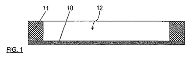
埋め込み加工品の製造方法の一実施形態を、工程の順に図1乃至図5に断面図で示す。即ち、第1被覆層10と、貫通孔12を有して第1被覆層10に貼着されたスペーサー層11とを図1に示す。スペーサー層11は第1被覆層10に積層されており、接着材を使用して第1被覆層10に恒久的に接着されている(より詳細に図示せず)。次に部品集合が貫通孔12内へ配置される。
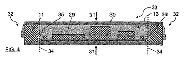
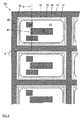
図4に示されるような次の工程では、第2被覆層30がスペーサー層11と充填材29とに貼り付けられる。それから、矢印31で示されるような平面に作用する圧力が第1被覆層10及び第2被覆層30に印加されることにより、スペーサー層11と第2被覆層30との間の過剰な充填材29が、層の縁の領域32に出る。ここではより詳細に図示しない方法の実施形態では、外面の縁を始点として第2被覆層30が傾斜してスペーサー層11に貼着されているので、充填材29が容易に排出される。第1及び第2被覆層10、30がスペーサー層に強固に密着接合される場合には、充填材29が熱衝撃によって固化され、半完成品33が形成される。次に、貫通孔12の内側輪郭35と部品集合13の外側輪郭36との間に位置する仕切り線34に沿って、半完成品33から図5に示す埋め込み加工品37が分離される。
埋め込み加工品41の更なる実施形態を図7に示しており、埋め込み加工品41は、部品集合13及び固化した充填材29によって構成されているに過ぎない。埋め込み加工品41が積層体から分離される前または後に、固化した充填材29から被覆層(図示せずが)除去される。
Claims (24)
- 少なくとも2つの電子部品(14,15,16,17)を有し、特にICカード、カード型商品券、身分証明書等のための埋め込み加工品(37,41)の製造方法において、
全ての電子部品を保持基板(18,22,27)上に相互に関連付けて配置することにより部品集合(13,21,26)を形成し、
前記部品集合を第1被覆層(10)上に配置した後、貫通孔(12)を有したスペーサー層(11)を前記第1被覆層に貼着し、
前記部品集合を前記貫通孔に収容し、
前記貫通孔を少なくとも部分的に満たす充填材(29)を前記貫通孔に導入し、
前記スペーサー層に第2被覆層(30,49)を貼着し、
前記被覆層を加圧しながら前記充填材を固化させることを特徴とする埋め込み加工品の製造方法。 - 少なくとも2つの電子部品(14,15,16,17)を有し、特にICカード、カード型商品券、身分証明書等のための埋め込み加工品(37,41)の製造方法において、
全ての電子部品を保持基板(18,22,27)上に相互に関連付けて配置することにより部品集合(13,21,26)を形成し、
貫通孔(12)を有したスペーサー層(11)を第1被覆層(10)に貼着した後、前記部品集合を該第1被覆層上に配設し、
前記部品集合を前記貫通孔に収容し、
前記貫通孔を少なくとも部分的に満たす充填材(29)を前記貫通孔に導入し、
前記スペーサー層に第2被覆層(30,49)を貼着し、
前記被覆層を加圧しながら前記充填材を固化させることを特徴とする埋め込み加工品の製造方法。 - 前記第1被覆層(10)に前記部品集合(26)を実装するため、
第1の量の充填材(57)を前記貫通孔(12)に導入し、
前記充填材中に前記電子部品(14,15,16,17)を相互に関連付けて配置し、
前記充填材を固化させて前記保持基板(27)を形成することを特徴とする、請求項1または2に記載の製造方法。 - 前記充填材(29,57)の固化は、前記部品(14,15,16,17)を損傷する温度を超えない温度の熱衝撃によって行うことを特徴とする、請求項1乃至3のいずれかに記載の製造方法。
- 前記部品集合(13,21,26)は前記第1被覆層(10)上に固定されることを特徴とする、請求項1乃至4のいずれかに記載の製造方法。
- 前記第1被覆層(10)上への部品集合(13,21,26)の固定は、前記部品集合の底面と前記第1被覆層との間に介装される固定層(20)を使用して行うことを特徴とする、請求項5に記載の製造方法。
- 前記第1被覆層上への前記部品集合(13,21,26)の固定は、超音波を使用して行うことを特徴とする、請求項5に記載の製造方法。
- 前記第1被覆層(10)上への前記部品集合(13,21,26)の固定は、熱的方法を利用して行うことを特徴とする、請求項5に記載の製造方法。
- 少なくとも1つの部品は表示素子(51)として実装され、前記表示素子と前記第2被覆層(49)との間に透明層(52)が配設されることを特徴とする、請求項1乃至8のいずれかに記載の製造方法。
- 前記被覆層(10,30,49)は、前記スペーサー層(11)に恒久的に接着されることを特徴とする、請求項1乃至9のいずれかに記載の製造方法。
- 前記埋め込み加工品(37,41)が、前記被覆層及び前記スペーサー層を有する積層体から分離される前または後に、前記第1及び・または第2被覆層(10,30)が、前記スペーサー層(11)及び・または固化した前記充填材(29,57)から除去されることを特徴とする、請求項1から10のいずれかに記載の製造方法。
- 前記埋め込み加工品は、前記貫通孔の内側輪郭(35)と前記部品集合(13,21)の外側輪郭(36)との間に仕切り線(34)が生じるようにして、前記積層体から分離されることを特徴とする、請求項1乃至11のいずれかに記載の製造方法。
- 少なくとも2つの電子部品(14,15,16,17)を有し、特にICカード、カード型商品券、身分証明書等のための埋め込み加工品(37,48)を製造するための半完成品(33)において、 全ての電子部品が、相互に関連付けられて保持基板(18,22,27)に配置されることにより部品集合(13,21,26)が形成されており、
前記部品集合はスペーサー層(11)の貫通孔(12)に収容され、
前記貫通孔は固化した充填材(29,57)によって満たされていることを特徴とする埋め込み加工品を製造するための半完成品。 - 前記貫通孔(12)を有する前記スペーサー層(11)は第1被覆層(10)に貼着され、
前記部品集合(13,21,26)は該第1被覆層上に配設されることを特徴とする、請求項13に記載の半完成品。 - 前記貫通孔の内側輪郭(35)と前記部品集合の外側輪郭(36)との間に仕切り線(34)が形成されることを特徴とする、請求項13または14に記載の半完成品。
- 前記第1被覆層(10)に対面する前記保持基板(22)の接触面に表面構造(24)が形成されることを特徴とする、請求項13乃至15のいずれかに記載の半完成品。
- 少なくとも1つの被覆層(10,30,49)は透明であることを特徴とする、請求項13乃至16のいずれかに記載の半完成品。
- 前記半完成品は板材(42)から形成され、
少なくとも1つ以上の部品集合(13,21,26)と、
1つの貫通孔(12)と、
1つの固化した充填材(29,57)と、
を有することを特徴とする、請求項13乃至17のいずれかに記載の半完成品。 - 請求項13乃至18のいずれかに記載の半完成品(33)を使用する、特にICカード、カード型商品券、身分証明書等であって、
カード(40,44,45)及び・または埋め込み加工品(37,41)を積層体から分離する前または後に接着材を用いて前記半完成品及び・または前記埋め込み加工品に少なくとも1つの外側層(38,39,45,46,54)を接着するカードの製造方法において、
前記カード及び・または前記埋め込み加工品は、スペーサー層(11)の貫通孔(12)の内側輪郭(35)と、前記貫通孔内に配設された部品集合(13,21,26)の外側輪郭(36)との間に仕切り線(34)が形成されるように前記積層体から分離されることを特徴とするカードの製造方法。 - 前記第1及び・または第2被覆層(40,44,45)は、前記外側層(38,39,45,46,54)を貼着する前に、前記スペーサー層(11)及び・または固化した前記充填材(29,57)から除去されることを特徴とする、請求項18に記載の製造方法。
- 前記接着材は、前記部品(14,15,16,17)を損傷する温度を超えない温度の熱衝撃によって活性化されることを特徴とする、請求項18または19に記載の製造方法。
- 請求項13乃至18のいずれかに記載の半完成品を含む、特にICカード、カード型商品券、身分証明書等のカード(40,44,45)において、
少なくとも1つの印刷可能な外側層(45,46,54)が、前記半完成品(33)を含む積層体に貼着されていることを特徴とするカード。 - 前記外側層(45,54)は、少なくとも一部の領域(50)において透明であることを特徴とする、請求項22に記載のカード。
- 前記外側層(54)は、前記充填材(29,57)と対面する面(56)に印刷が施されることを特徴とする、請求項23に記載のカード。
Applications Claiming Priority (3)
| Application Number | Priority Date | Filing Date | Title |
|---|---|---|---|
| DE102007008487.2 | 2007-02-19 | ||
| DE102007008487A DE102007008487A1 (de) | 2007-02-19 | 2007-02-19 | Verfahren und Halbzeug zur Herstellung eines Inlays |
| PCT/EP2007/010190 WO2008101529A1 (de) | 2007-02-19 | 2007-11-23 | Verfahren und halbzeug zur herstellung eines inlays |
Publications (2)
| Publication Number | Publication Date |
|---|---|
| JP2010519614A true JP2010519614A (ja) | 2010-06-03 |
| JP5424898B2 JP5424898B2 (ja) | 2014-02-26 |
Family
ID=39111556
Family Applications (1)
| Application Number | Title | Priority Date | Filing Date |
|---|---|---|---|
| JP2009549779A Active JP5424898B2 (ja) | 2007-02-19 | 2007-11-23 | 埋め込み加工品のための半完成品及び方法 |
Country Status (9)
| Country | Link |
|---|---|
| US (1) | US8305764B2 (ja) |
| EP (1) | EP1989667B1 (ja) |
| JP (1) | JP5424898B2 (ja) |
| KR (1) | KR20090118066A (ja) |
| AT (1) | ATE540376T1 (ja) |
| CA (1) | CA2675660C (ja) |
| DE (1) | DE102007008487A1 (ja) |
| ES (1) | ES2377150T3 (ja) |
| WO (1) | WO2008101529A1 (ja) |
Cited By (2)
| Publication number | Priority date | Publication date | Assignee | Title |
|---|---|---|---|---|
| JP2015509291A (ja) * | 2012-01-31 | 2015-03-26 | コミサリア ア レネルジー アトミック エ オ ゼネルジー アルテルナティブCommissariat Al’Energie Atomique Et Aux Energiesalternatives | マイクロ電子チップ要素をワイヤ要素に組み付けるための方法、および組み付けが行われることを可能にする設備 |
| JP2021536677A (ja) * | 2018-09-04 | 2021-12-27 | ピルキントン グループ リミテッド | 電気装置、電気装置を含む中間層プライ、および当該電気装置および中間層プライを製造するための方法 |
Families Citing this family (29)
| Publication number | Priority date | Publication date | Assignee | Title |
|---|---|---|---|---|
| FR2944121B1 (fr) * | 2009-04-03 | 2016-06-24 | Paragon Identification | Carte d'identification de radio frequence(rfid) semi-rigide, le procede de fabrication et la machine permettant sa fabrication |
| JP5766920B2 (ja) * | 2009-08-31 | 2015-08-19 | トッパン・フォームズ株式会社 | 非接触型データ受送信体の製造方法 |
| DE102009050753A1 (de) | 2009-10-27 | 2011-04-28 | Giesecke & Devrient Gmbh | Verfahren zur Herstellung von Inlays für kartenförmige Datenträger |
| DE102012001346A1 (de) * | 2012-01-24 | 2013-07-25 | Giesecke & Devrient Gmbh | Verfahren zum Herstellen eines Datenträgers |
| US8403766B2 (en) * | 2012-06-22 | 2013-03-26 | Tinsley Transfers, Inc. | Prosthetic appliance transfer kit and method |
| US10032099B2 (en) | 2012-07-20 | 2018-07-24 | CPI Card Group—Colorado, Inc. | Weighted transaction card |
| US8857722B2 (en) | 2012-07-20 | 2014-10-14 | CPI Card Group—Colorado, Inc. | Weighted transaction card |
| US20170243104A1 (en) * | 2013-03-14 | 2017-08-24 | X-Card Holdings, Llc | Information carrying card for displaying one time passcodes, and method of making the same |
| DE102013008506A1 (de) * | 2013-05-16 | 2014-11-20 | Giesecke & Devrient Gmbh | Herstellungsverfahren für tragbare Datenträger |
| WO2015061611A1 (en) | 2013-10-25 | 2015-04-30 | Cpi Card Group - Colorado, Inc. | Multi-metal layered card |
| KR101596866B1 (ko) * | 2014-06-19 | 2016-02-23 | 하이쎌(주) | 스마트 카드 및 스마트 카드 제조 방법 |
| FR3045891A1 (fr) * | 2015-12-22 | 2017-06-23 | Oberthur Technologies | Procede de fabrication par lamination a chaud d'une carte a microcircuit comportant un flex dans une cavite et carte ainsi obtenue |
| WO2017210305A1 (en) | 2016-06-01 | 2017-12-07 | Cpi Card Group - Colorado, Inc. | Ic chip card with integrated biometric sensor pads |
| EP3582973B1 (en) | 2017-02-14 | 2023-06-28 | CPI Card Group - Colorado, Inc. | Edge-to-edge metal card and production method |
| WO2019224575A1 (en) | 2018-05-22 | 2019-11-28 | Tyco Fire & Security Gmbh | Elongate flexible tag |
| EP3651068A1 (fr) | 2018-11-12 | 2020-05-13 | Thales Dis France SA | Procédé de réalisation d'un insert électronique pour support portable multi-composants et insert obtenu |
| FR3099299B1 (fr) * | 2019-07-24 | 2021-08-06 | Commissariat Energie Atomique | Moule d’assemblage pour fabriquer un dispotitif tridimensionnel comprenant plusieurs composants microelectroniques |
| US12223814B2 (en) | 2019-09-16 | 2025-02-11 | Sensormatic Electronics, LLC | Security tag for textiles using conductive thread |
| US10783424B1 (en) | 2019-09-18 | 2020-09-22 | Sensormatic Electronics, LLC | Systems and methods for providing tags adapted to be incorporated with or in items |
| US11443160B2 (en) | 2019-09-18 | 2022-09-13 | Sensormatic Electronics, LLC | Systems and methods for laser tuning and attaching RFID tags to products |
| US11055588B2 (en) | 2019-11-27 | 2021-07-06 | Sensormatic Electronics, LLC | Flexible water-resistant sensor tag |
| US12524640B2 (en) | 2019-11-27 | 2026-01-13 | Sensormatic Electronics, LLC | Flexible water-resistant sensor tag |
| US11738482B2 (en) * | 2020-11-16 | 2023-08-29 | Jack Armstrong | Method of potting electrical components into complex finished forms |
| US11755874B2 (en) | 2021-03-03 | 2023-09-12 | Sensormatic Electronics, LLC | Methods and systems for heat applied sensor tag |
| US11869324B2 (en) | 2021-12-23 | 2024-01-09 | Sensormatic Electronics, LLC | Securing a security tag into an article |
| US12536401B2 (en) | 2022-08-31 | 2026-01-27 | Sensormatic Electronics, LLC | Security tag |
| US12220897B2 (en) | 2022-10-20 | 2025-02-11 | X-Card Holdings, Llc | Core layer for information carrying card, resulting information carrying card, and methods of making the same |
| US12528279B2 (en) | 2022-10-20 | 2026-01-20 | X-Card Holdings, Llc | Core layer for information carrying card, resulting information carrying card, and methods of making the same |
| WO2025207767A1 (en) * | 2024-03-28 | 2025-10-02 | Sentrycard Technologies, Inc. | Core layer comprising system-in-package, resulting information carrying card, and methods of making the same |
Citations (7)
| Publication number | Priority date | Publication date | Assignee | Title |
|---|---|---|---|---|
| JPS60122456A (ja) * | 1984-07-31 | 1985-06-29 | Casio Comput Co Ltd | 小型電子機器 |
| JPH05246185A (ja) * | 1992-03-05 | 1993-09-24 | Ryoden Kasei Co Ltd | Icカード及びその製造方法 |
| JPH06122297A (ja) * | 1992-08-31 | 1994-05-06 | Sony Chem Corp | Icカード及びその製造方法 |
| JPH0836629A (ja) * | 1994-02-24 | 1996-02-06 | Gemplus Card Internatl Sa | 非接触式カードの製造方法 |
| JPH0880696A (ja) * | 1994-07-15 | 1996-03-26 | Shinko Name Plate Kk | メモリカード及びその製造方法 |
| JPH08235335A (ja) * | 1995-02-27 | 1996-09-13 | Toshiba Corp | 電子部品内蔵カードの製造方法 |
| JPH09275184A (ja) * | 1995-06-29 | 1997-10-21 | Hitachi Maxell Ltd | 情報担体及びその製造方法 |
Family Cites Families (19)
| Publication number | Priority date | Publication date | Assignee | Title |
|---|---|---|---|---|
| DE3248385A1 (de) * | 1982-12-28 | 1984-06-28 | GAO Gesellschaft für Automation und Organisation mbH, 8000 München | Ausweiskarte mit integriertem schaltkreis |
| JPS61273786A (ja) * | 1985-05-29 | 1986-12-04 | Pilot Pen Co Ltd:The | 可視磁気カ−ド |
| JP2602343B2 (ja) * | 1990-05-07 | 1997-04-23 | 三菱電機株式会社 | Icカード |
| US5261987A (en) * | 1992-06-05 | 1993-11-16 | Eastman Kodak Company | Method of making an identification card |
| JP2774906B2 (ja) * | 1992-09-17 | 1998-07-09 | 三菱電機株式会社 | 薄形半導体装置及びその製造方法 |
| US5612513A (en) | 1995-09-19 | 1997-03-18 | Micron Communications, Inc. | Article and method of manufacturing an enclosed electrical circuit using an encapsulant |
| US6050494A (en) * | 1997-06-09 | 2000-04-18 | Samsung Display Devices Co., Ltd. | Smart card |
| JP3652488B2 (ja) * | 1997-12-18 | 2005-05-25 | Tdk株式会社 | 樹脂パッケージの製造方法 |
| US6524517B1 (en) * | 1999-12-15 | 2003-02-25 | Nanogen, Inc. | Methods for molding and grafting highly uniform polymer layers onto electronic microchips |
| EP1152368B1 (de) * | 2000-05-05 | 2010-07-14 | Infineon Technologies AG | Chipkarte |
| JP2002279384A (ja) * | 2001-03-19 | 2002-09-27 | Toshiba Corp | 携帯可能電子媒体及びその製造方法 |
| FI111039B (fi) * | 2001-04-06 | 2003-05-15 | Rafsec Oy | Älykorttiraina ja menetelmä sen valmistamiseksi |
| DE10324043B4 (de) * | 2003-05-27 | 2006-08-31 | Giesecke & Devrient Gmbh | Kartenförmiger elektronischer Datenträger, Funktionsinlett dafür und ihre Herstellungsverfahren |
| JP2005122678A (ja) * | 2003-09-26 | 2005-05-12 | Toshiba Corp | 携帯可能電子装置 |
| DE10346474B4 (de) * | 2003-10-02 | 2014-07-10 | Infineon Technologies Ag | Sensorbauteil mit einem Sensorchip, Sensorstapel und Verfahren zum Prüfen einer biochemischen Probe |
| US7663214B2 (en) * | 2005-07-25 | 2010-02-16 | Kingston Technology Corporation | High-capacity memory card and method of making the same |
| US20090020615A1 (en) * | 2006-02-21 | 2009-01-22 | Patel Gordhanbhai N | Method of making smart cards with an excapsulant |
| US7948765B2 (en) * | 2006-08-11 | 2011-05-24 | Bunn-O-Matic Corporation | Reconfigurable control panel |
| US8028923B2 (en) * | 2007-11-14 | 2011-10-04 | Smartrac Ip B.V. | Electronic inlay structure and method of manufacture thereof |
-
2007
- 2007-02-19 DE DE102007008487A patent/DE102007008487A1/de not_active Ceased
- 2007-11-23 US US12/279,825 patent/US8305764B2/en active Active
- 2007-11-23 AT AT07846790T patent/ATE540376T1/de active
- 2007-11-23 KR KR1020097019479A patent/KR20090118066A/ko not_active Ceased
- 2007-11-23 CA CA2675660A patent/CA2675660C/en active Active
- 2007-11-23 ES ES07846790T patent/ES2377150T3/es active Active
- 2007-11-23 WO PCT/EP2007/010190 patent/WO2008101529A1/de not_active Ceased
- 2007-11-23 JP JP2009549779A patent/JP5424898B2/ja active Active
- 2007-11-23 EP EP07846790A patent/EP1989667B1/de active Active
Patent Citations (7)
| Publication number | Priority date | Publication date | Assignee | Title |
|---|---|---|---|---|
| JPS60122456A (ja) * | 1984-07-31 | 1985-06-29 | Casio Comput Co Ltd | 小型電子機器 |
| JPH05246185A (ja) * | 1992-03-05 | 1993-09-24 | Ryoden Kasei Co Ltd | Icカード及びその製造方法 |
| JPH06122297A (ja) * | 1992-08-31 | 1994-05-06 | Sony Chem Corp | Icカード及びその製造方法 |
| JPH0836629A (ja) * | 1994-02-24 | 1996-02-06 | Gemplus Card Internatl Sa | 非接触式カードの製造方法 |
| JPH0880696A (ja) * | 1994-07-15 | 1996-03-26 | Shinko Name Plate Kk | メモリカード及びその製造方法 |
| JPH08235335A (ja) * | 1995-02-27 | 1996-09-13 | Toshiba Corp | 電子部品内蔵カードの製造方法 |
| JPH09275184A (ja) * | 1995-06-29 | 1997-10-21 | Hitachi Maxell Ltd | 情報担体及びその製造方法 |
Cited By (3)
| Publication number | Priority date | Publication date | Assignee | Title |
|---|---|---|---|---|
| JP2015509291A (ja) * | 2012-01-31 | 2015-03-26 | コミサリア ア レネルジー アトミック エ オ ゼネルジー アルテルナティブCommissariat Al’Energie Atomique Et Aux Energiesalternatives | マイクロ電子チップ要素をワイヤ要素に組み付けるための方法、および組み付けが行われることを可能にする設備 |
| JP2021536677A (ja) * | 2018-09-04 | 2021-12-27 | ピルキントン グループ リミテッド | 電気装置、電気装置を含む中間層プライ、および当該電気装置および中間層プライを製造するための方法 |
| JP7604364B2 (ja) | 2018-09-04 | 2024-12-23 | ピルキントン グループ リミテッド | 電気装置、電気装置を含む中間層プライ、および当該電気装置および中間層プライを製造するための方法 |
Also Published As
| Publication number | Publication date |
|---|---|
| EP1989667B1 (de) | 2012-01-04 |
| WO2008101529A8 (de) | 2008-10-16 |
| CA2675660A1 (en) | 2008-08-28 |
| CA2675660C (en) | 2013-03-05 |
| WO2008101529A1 (de) | 2008-08-28 |
| KR20090118066A (ko) | 2009-11-17 |
| DE102007008487A1 (de) | 2008-08-21 |
| US8305764B2 (en) | 2012-11-06 |
| EP1989667A1 (de) | 2008-11-12 |
| JP5424898B2 (ja) | 2014-02-26 |
| US20100226107A1 (en) | 2010-09-09 |
| ATE540376T1 (de) | 2012-01-15 |
| ES2377150T3 (es) | 2012-03-22 |
Similar Documents
| Publication | Publication Date | Title |
|---|---|---|
| JP5424898B2 (ja) | 埋め込み加工品のための半完成品及び方法 | |
| JP5395660B2 (ja) | 少なくとも1つの電子モジュールを備えるカードを製造する方法、本方法中に製作されるアセンブリ、及び中間生成物 | |
| JP5209602B2 (ja) | 電子カードおよび電子タグ用の電子埋込物モジュール | |
| KR102481332B1 (ko) | 칩 카드 제조 방법, 및 상기 방법에 의해 획득된 칩 카드 | |
| CN101662965A (zh) | 内置rfid标签的游戏代用币及其制造方法 | |
| JP5181724B2 (ja) | Icカード及びその製造方法 | |
| US5851854A (en) | Method for producing a data carrier | |
| KR102883917B1 (ko) | 직물에 스마트 카드를 연결하기 위한 장치 및 플렉시블 스마트 카드 형식의 전자 카드 제조 방법 | |
| EP2141973A1 (en) | Method of providing conductive structures in a multi-foil system and multi-foil system comprising same | |
| JP2012044163A (ja) | 電気的構成要素を埋め込む方法 | |
| JP2000148949A (ja) | 非接触icカードおよびその製造方法 | |
| JP5369496B2 (ja) | 非接触icカードの製造方法 | |
| JP2000331138A (ja) | 非接触型icカード | |
| JP7719761B2 (ja) | 多層チップカードを製造する方法および多層チップカード | |
| JP2010128934A (ja) | Rfidインレット、rfidタグ、rfidタグを製造する方法、rfidタグを含むプリント基板、および、プリント基板にrfidタグを埋め込む方法 | |
| JP2010257416A (ja) | 情報記録媒体、非接触型ic付データキャリア、および情報記録媒体の製造方法 | |
| JP2014160327A (ja) | 積層体、積層体製造方法 | |
| JP5853509B2 (ja) | 枠体付電子部品、枠体付電子部品の製造方法、カードの製造方法、カード | |
| KR100552565B1 (ko) | 호일 적층을 통한 콤비형 ic 카드 반제품 및 그 제조방법 | |
| JP3930601B2 (ja) | Icカードおよびその製造方法 | |
| JP5870564B2 (ja) | 電子部品一体シートの製造方法、カードの製造方法、電子部品一体シート、カード | |
| JP3871762B2 (ja) | Icカードおよびその製造方法 | |
| JPH1067194A (ja) | 情報記録媒体 | |
| KR100968139B1 (ko) | 디스플레이카드의 제조방법 | |
| JP2023165242A (ja) | カバー付き非接触icインレット、冊子、カバー付き非接触icインレットの製造方法および非接触icインレット |
Legal Events
| Date | Code | Title | Description |
|---|---|---|---|
| A977 | Report on retrieval |
Free format text: JAPANESE INTERMEDIATE CODE: A971007 Effective date: 20111125 |
|
| A131 | Notification of reasons for refusal |
Free format text: JAPANESE INTERMEDIATE CODE: A131 Effective date: 20111130 |
|
| A601 | Written request for extension of time |
Free format text: JAPANESE INTERMEDIATE CODE: A601 Effective date: 20120229 |
|
| A602 | Written permission of extension of time |
Free format text: JAPANESE INTERMEDIATE CODE: A602 Effective date: 20120309 |
|
| A601 | Written request for extension of time |
Free format text: JAPANESE INTERMEDIATE CODE: A601 Effective date: 20120330 |
|
| A602 | Written permission of extension of time |
Free format text: JAPANESE INTERMEDIATE CODE: A602 Effective date: 20120406 |
|
| A521 | Request for written amendment filed |
Free format text: JAPANESE INTERMEDIATE CODE: A523 Effective date: 20120419 |
|
| A02 | Decision of refusal |
Free format text: JAPANESE INTERMEDIATE CODE: A02 Effective date: 20120912 |
|
| A521 | Request for written amendment filed |
Free format text: JAPANESE INTERMEDIATE CODE: A523 Effective date: 20130115 |
|
| A521 | Request for written amendment filed |
Free format text: JAPANESE INTERMEDIATE CODE: A821 Effective date: 20130116 |
|
| A911 | Transfer to examiner for re-examination before appeal (zenchi) |
Free format text: JAPANESE INTERMEDIATE CODE: A911 Effective date: 20130207 |
|
| A912 | Re-examination (zenchi) completed and case transferred to appeal board |
Free format text: JAPANESE INTERMEDIATE CODE: A912 Effective date: 20130412 |
|
| A61 | First payment of annual fees (during grant procedure) |
Free format text: JAPANESE INTERMEDIATE CODE: A61 Effective date: 20131126 |
|
| R150 | Certificate of patent or registration of utility model |
Free format text: JAPANESE INTERMEDIATE CODE: R150 Ref document number: 5424898 Country of ref document: JP Free format text: JAPANESE INTERMEDIATE CODE: R150 |
|
| R250 | Receipt of annual fees |
Free format text: JAPANESE INTERMEDIATE CODE: R250 |
|
| R250 | Receipt of annual fees |
Free format text: JAPANESE INTERMEDIATE CODE: R250 |
|
| R250 | Receipt of annual fees |
Free format text: JAPANESE INTERMEDIATE CODE: R250 |
|
| S111 | Request for change of ownership or part of ownership |
Free format text: JAPANESE INTERMEDIATE CODE: R313113 |
|
| S531 | Written request for registration of change of domicile |
Free format text: JAPANESE INTERMEDIATE CODE: R313531 |
|
| R350 | Written notification of registration of transfer |
Free format text: JAPANESE INTERMEDIATE CODE: R350 |
|
| R250 | Receipt of annual fees |
Free format text: JAPANESE INTERMEDIATE CODE: R250 |
|
| R250 | Receipt of annual fees |
Free format text: JAPANESE INTERMEDIATE CODE: R250 |
|
| R250 | Receipt of annual fees |
Free format text: JAPANESE INTERMEDIATE CODE: R250 |
|
| R250 | Receipt of annual fees |
Free format text: JAPANESE INTERMEDIATE CODE: R250 |
|
| R250 | Receipt of annual fees |
Free format text: JAPANESE INTERMEDIATE CODE: R250 |
|
| R250 | Receipt of annual fees |
Free format text: JAPANESE INTERMEDIATE CODE: R250 |
|
| R250 | Receipt of annual fees |
Free format text: JAPANESE INTERMEDIATE CODE: R250 |