JP2010517261A - ELECTRONIC FIELD EFFECT DEVICE AND METHOD FOR MANUFACTURING THE SAME - Google Patents
ELECTRONIC FIELD EFFECT DEVICE AND METHOD FOR MANUFACTURING THE SAME Download PDFInfo
- Publication number
- JP2010517261A JP2010517261A JP2009546060A JP2009546060A JP2010517261A JP 2010517261 A JP2010517261 A JP 2010517261A JP 2009546060 A JP2009546060 A JP 2009546060A JP 2009546060 A JP2009546060 A JP 2009546060A JP 2010517261 A JP2010517261 A JP 2010517261A
- Authority
- JP
- Japan
- Prior art keywords
- layer
- field effect
- diamond
- effect device
- interface
- Prior art date
- Legal status (The legal status is an assumption and is not a legal conclusion. Google has not performed a legal analysis and makes no representation as to the accuracy of the status listed.)
- Pending
Links
- 238000000034 method Methods 0.000 title claims abstract description 39
- 230000005669 field effect Effects 0.000 title claims abstract description 38
- 238000004519 manufacturing process Methods 0.000 title abstract description 10
- 239000010432 diamond Substances 0.000 claims abstract description 253
- 229910003460 diamond Inorganic materials 0.000 claims abstract description 249
- 239000000463 material Substances 0.000 claims abstract description 54
- 239000002800 charge carrier Substances 0.000 claims abstract description 45
- 230000010287 polarization Effects 0.000 claims description 71
- 230000005684 electric field Effects 0.000 claims description 36
- 238000005229 chemical vapour deposition Methods 0.000 claims description 26
- 239000013078 crystal Substances 0.000 claims description 21
- 230000008569 process Effects 0.000 claims description 11
- 238000005530 etching Methods 0.000 claims description 7
- 230000002301 combined effect Effects 0.000 claims description 6
- 238000000151 deposition Methods 0.000 claims description 6
- 230000008021 deposition Effects 0.000 claims description 4
- 238000001020 plasma etching Methods 0.000 claims description 3
- 238000004854 X-ray topography Methods 0.000 claims description 2
- 238000005304 joining Methods 0.000 claims description 2
- 238000006073 displacement reaction Methods 0.000 claims 1
- 239000007789 gas Substances 0.000 abstract description 8
- 239000010410 layer Substances 0.000 description 523
- 238000005036 potential barrier Methods 0.000 description 19
- 239000000969 carrier Substances 0.000 description 16
- 230000005428 wave function Effects 0.000 description 13
- 230000015572 biosynthetic process Effects 0.000 description 12
- 238000009792 diffusion process Methods 0.000 description 10
- 238000003786 synthesis reaction Methods 0.000 description 10
- ZOXJGFHDIHLPTG-UHFFFAOYSA-N Boron Chemical compound [B] ZOXJGFHDIHLPTG-UHFFFAOYSA-N 0.000 description 9
- 238000010586 diagram Methods 0.000 description 9
- 239000000758 substrate Substances 0.000 description 9
- 229910052796 boron Inorganic materials 0.000 description 8
- 230000007704 transition Effects 0.000 description 8
- 230000008901 benefit Effects 0.000 description 7
- 239000002019 doping agent Substances 0.000 description 7
- 230000000694 effects Effects 0.000 description 7
- IJGRMHOSHXDMSA-UHFFFAOYSA-N Atomic nitrogen Chemical compound N#N IJGRMHOSHXDMSA-UHFFFAOYSA-N 0.000 description 6
- 239000004065 semiconductor Substances 0.000 description 6
- 238000012546 transfer Methods 0.000 description 6
- 239000000370 acceptor Substances 0.000 description 5
- 125000004429 atom Chemical group 0.000 description 5
- 230000015556 catabolic process Effects 0.000 description 5
- 230000008859 change Effects 0.000 description 5
- 239000012159 carrier gas Substances 0.000 description 4
- 230000007547 defect Effects 0.000 description 4
- 239000004047 hole gas Substances 0.000 description 4
- 238000012545 processing Methods 0.000 description 4
- YZCKVEUIGOORGS-UHFFFAOYSA-N Hydrogen atom Chemical compound [H] YZCKVEUIGOORGS-UHFFFAOYSA-N 0.000 description 3
- 238000005275 alloying Methods 0.000 description 3
- 239000002131 composite material Substances 0.000 description 3
- 238000011065 in-situ storage Methods 0.000 description 3
- 229910052757 nitrogen Inorganic materials 0.000 description 3
- 230000005533 two-dimensional electron gas Effects 0.000 description 3
- 229910002704 AlGaN Inorganic materials 0.000 description 2
- 229910001218 Gallium arsenide Inorganic materials 0.000 description 2
- OAICVXFJPJFONN-UHFFFAOYSA-N Phosphorus Chemical compound [P] OAICVXFJPJFONN-UHFFFAOYSA-N 0.000 description 2
- 229910004298 SiO 2 Inorganic materials 0.000 description 2
- 229910052782 aluminium Inorganic materials 0.000 description 2
- 230000004888 barrier function Effects 0.000 description 2
- PMHQVHHXPFUNSP-UHFFFAOYSA-M copper(1+);methylsulfanylmethane;bromide Chemical compound Br[Cu].CSC PMHQVHHXPFUNSP-UHFFFAOYSA-M 0.000 description 2
- 238000013461 design Methods 0.000 description 2
- 230000001627 detrimental effect Effects 0.000 description 2
- 229910021480 group 4 element Inorganic materials 0.000 description 2
- 230000005525 hole transport Effects 0.000 description 2
- 229910052739 hydrogen Inorganic materials 0.000 description 2
- 238000005984 hydrogenation reaction Methods 0.000 description 2
- 238000005468 ion implantation Methods 0.000 description 2
- 238000003754 machining Methods 0.000 description 2
- 238000002488 metal-organic chemical vapour deposition Methods 0.000 description 2
- 125000004433 nitrogen atom Chemical group N* 0.000 description 2
- 229910052760 oxygen Inorganic materials 0.000 description 2
- 229910052698 phosphorus Inorganic materials 0.000 description 2
- 239000011574 phosphorus Substances 0.000 description 2
- 238000005240 physical vapour deposition Methods 0.000 description 2
- 238000005381 potential energy Methods 0.000 description 2
- 238000002360 preparation method Methods 0.000 description 2
- 230000002269 spontaneous effect Effects 0.000 description 2
- 239000000126 substance Substances 0.000 description 2
- 230000005641 tunneling Effects 0.000 description 2
- 229910018509 Al—N Inorganic materials 0.000 description 1
- 229910052582 BN Inorganic materials 0.000 description 1
- PZNSFCLAULLKQX-UHFFFAOYSA-N Boron nitride Chemical compound N#B PZNSFCLAULLKQX-UHFFFAOYSA-N 0.000 description 1
- UFHFLCQGNIYNRP-UHFFFAOYSA-N Hydrogen Chemical compound [H][H] UFHFLCQGNIYNRP-UHFFFAOYSA-N 0.000 description 1
- 208000013201 Stress fracture Diseases 0.000 description 1
- 230000004913 activation Effects 0.000 description 1
- 239000000956 alloy Substances 0.000 description 1
- 229910045601 alloy Inorganic materials 0.000 description 1
- 229910021486 amorphous silicon dioxide Inorganic materials 0.000 description 1
- 230000003321 amplification Effects 0.000 description 1
- QVGXLLKOCUKJST-UHFFFAOYSA-N atomic oxygen Chemical compound [O] QVGXLLKOCUKJST-UHFFFAOYSA-N 0.000 description 1
- 230000000903 blocking effect Effects 0.000 description 1
- 239000007767 bonding agent Substances 0.000 description 1
- -1 boron ions Chemical class 0.000 description 1
- 150000001722 carbon compounds Chemical class 0.000 description 1
- 238000003486 chemical etching Methods 0.000 description 1
- 239000013626 chemical specie Substances 0.000 description 1
- 238000007796 conventional method Methods 0.000 description 1
- 230000002708 enhancing effect Effects 0.000 description 1
- 230000001747 exhibiting effect Effects 0.000 description 1
- 229910052731 fluorine Inorganic materials 0.000 description 1
- BHEPBYXIRTUNPN-UHFFFAOYSA-N hydridophosphorus(.) (triplet) Chemical compound [PH] BHEPBYXIRTUNPN-UHFFFAOYSA-N 0.000 description 1
- 239000001257 hydrogen Substances 0.000 description 1
- 238000002513 implantation Methods 0.000 description 1
- 239000012535 impurity Substances 0.000 description 1
- 229910052738 indium Inorganic materials 0.000 description 1
- 239000011810 insulating material Substances 0.000 description 1
- 238000010884 ion-beam technique Methods 0.000 description 1
- 150000002500 ions Chemical class 0.000 description 1
- 238000000608 laser ablation Methods 0.000 description 1
- 239000011159 matrix material Substances 0.000 description 1
- 230000007246 mechanism Effects 0.000 description 1
- 229910052751 metal Inorganic materials 0.000 description 1
- 239000002184 metal Substances 0.000 description 1
- 238000003801 milling Methods 0.000 description 1
- 238000012986 modification Methods 0.000 description 1
- 230000004048 modification Effects 0.000 description 1
- 238000001451 molecular beam epitaxy Methods 0.000 description 1
- 238000003199 nucleic acid amplification method Methods 0.000 description 1
- 239000001301 oxygen Substances 0.000 description 1
- 238000005498 polishing Methods 0.000 description 1
- 238000007517 polishing process Methods 0.000 description 1
- 238000000926 separation method Methods 0.000 description 1
- 229910052710 silicon Inorganic materials 0.000 description 1
- 239000010703 silicon Substances 0.000 description 1
- 239000002356 single layer Substances 0.000 description 1
- 239000007787 solid Substances 0.000 description 1
- 230000003746 surface roughness Effects 0.000 description 1
- 229910052984 zinc sulfide Inorganic materials 0.000 description 1
Images


Classifications
-
- C—CHEMISTRY; METALLURGY
- C01—INORGANIC CHEMISTRY
- C01B—NON-METALLIC ELEMENTS; COMPOUNDS THEREOF; METALLOIDS OR COMPOUNDS THEREOF NOT COVERED BY SUBCLASS C01C
- C01B32/00—Carbon; Compounds thereof
- C01B32/25—Diamond
- C01B32/28—After-treatment, e.g. purification, irradiation, separation or recovery
-
- C—CHEMISTRY; METALLURGY
- C23—COATING METALLIC MATERIAL; COATING MATERIAL WITH METALLIC MATERIAL; CHEMICAL SURFACE TREATMENT; DIFFUSION TREATMENT OF METALLIC MATERIAL; COATING BY VACUUM EVAPORATION, BY SPUTTERING, BY ION IMPLANTATION OR BY CHEMICAL VAPOUR DEPOSITION, IN GENERAL; INHIBITING CORROSION OF METALLIC MATERIAL OR INCRUSTATION IN GENERAL
- C23C—COATING METALLIC MATERIAL; COATING MATERIAL WITH METALLIC MATERIAL; SURFACE TREATMENT OF METALLIC MATERIAL BY DIFFUSION INTO THE SURFACE, BY CHEMICAL CONVERSION OR SUBSTITUTION; COATING BY VACUUM EVAPORATION, BY SPUTTERING, BY ION IMPLANTATION OR BY CHEMICAL VAPOUR DEPOSITION, IN GENERAL
- C23C16/00—Chemical coating by decomposition of gaseous compounds, without leaving reaction products of surface material in the coating, i.e. chemical vapour deposition [CVD] processes
- C23C16/22—Chemical coating by decomposition of gaseous compounds, without leaving reaction products of surface material in the coating, i.e. chemical vapour deposition [CVD] processes characterised by the deposition of inorganic material, other than metallic material
- C23C16/26—Deposition of carbon only
- C23C16/27—Diamond only
- C23C16/274—Diamond only using microwave discharges
-
- C—CHEMISTRY; METALLURGY
- C23—COATING METALLIC MATERIAL; COATING MATERIAL WITH METALLIC MATERIAL; CHEMICAL SURFACE TREATMENT; DIFFUSION TREATMENT OF METALLIC MATERIAL; COATING BY VACUUM EVAPORATION, BY SPUTTERING, BY ION IMPLANTATION OR BY CHEMICAL VAPOUR DEPOSITION, IN GENERAL; INHIBITING CORROSION OF METALLIC MATERIAL OR INCRUSTATION IN GENERAL
- C23C—COATING METALLIC MATERIAL; COATING MATERIAL WITH METALLIC MATERIAL; SURFACE TREATMENT OF METALLIC MATERIAL BY DIFFUSION INTO THE SURFACE, BY CHEMICAL CONVERSION OR SUBSTITUTION; COATING BY VACUUM EVAPORATION, BY SPUTTERING, BY ION IMPLANTATION OR BY CHEMICAL VAPOUR DEPOSITION, IN GENERAL
- C23C16/00—Chemical coating by decomposition of gaseous compounds, without leaving reaction products of surface material in the coating, i.e. chemical vapour deposition [CVD] processes
- C23C16/22—Chemical coating by decomposition of gaseous compounds, without leaving reaction products of surface material in the coating, i.e. chemical vapour deposition [CVD] processes characterised by the deposition of inorganic material, other than metallic material
- C23C16/26—Deposition of carbon only
- C23C16/27—Diamond only
- C23C16/278—Diamond only doping or introduction of a secondary phase in the diamond
-
- C—CHEMISTRY; METALLURGY
- C30—CRYSTAL GROWTH
- C30B—SINGLE-CRYSTAL GROWTH; UNIDIRECTIONAL SOLIDIFICATION OF EUTECTIC MATERIAL OR UNIDIRECTIONAL DEMIXING OF EUTECTOID MATERIAL; REFINING BY ZONE-MELTING OF MATERIAL; PRODUCTION OF A HOMOGENEOUS POLYCRYSTALLINE MATERIAL WITH DEFINED STRUCTURE; SINGLE CRYSTALS OR HOMOGENEOUS POLYCRYSTALLINE MATERIAL WITH DEFINED STRUCTURE; AFTER-TREATMENT OF SINGLE CRYSTALS OR A HOMOGENEOUS POLYCRYSTALLINE MATERIAL WITH DEFINED STRUCTURE; APPARATUS THEREFOR
- C30B25/00—Single-crystal growth by chemical reaction of reactive gases, e.g. chemical vapour-deposition growth
- C30B25/02—Epitaxial-layer growth
- C30B25/10—Heating of the reaction chamber or the substrate
- C30B25/105—Heating of the reaction chamber or the substrate by irradiation or electric discharge
-
- C—CHEMISTRY; METALLURGY
- C30—CRYSTAL GROWTH
- C30B—SINGLE-CRYSTAL GROWTH; UNIDIRECTIONAL SOLIDIFICATION OF EUTECTIC MATERIAL OR UNIDIRECTIONAL DEMIXING OF EUTECTOID MATERIAL; REFINING BY ZONE-MELTING OF MATERIAL; PRODUCTION OF A HOMOGENEOUS POLYCRYSTALLINE MATERIAL WITH DEFINED STRUCTURE; SINGLE CRYSTALS OR HOMOGENEOUS POLYCRYSTALLINE MATERIAL WITH DEFINED STRUCTURE; AFTER-TREATMENT OF SINGLE CRYSTALS OR A HOMOGENEOUS POLYCRYSTALLINE MATERIAL WITH DEFINED STRUCTURE; APPARATUS THEREFOR
- C30B25/00—Single-crystal growth by chemical reaction of reactive gases, e.g. chemical vapour-deposition growth
- C30B25/02—Epitaxial-layer growth
- C30B25/18—Epitaxial-layer growth characterised by the substrate
- C30B25/20—Epitaxial-layer growth characterised by the substrate the substrate being of the same materials as the epitaxial layer
-
- C—CHEMISTRY; METALLURGY
- C30—CRYSTAL GROWTH
- C30B—SINGLE-CRYSTAL GROWTH; UNIDIRECTIONAL SOLIDIFICATION OF EUTECTIC MATERIAL OR UNIDIRECTIONAL DEMIXING OF EUTECTOID MATERIAL; REFINING BY ZONE-MELTING OF MATERIAL; PRODUCTION OF A HOMOGENEOUS POLYCRYSTALLINE MATERIAL WITH DEFINED STRUCTURE; SINGLE CRYSTALS OR HOMOGENEOUS POLYCRYSTALLINE MATERIAL WITH DEFINED STRUCTURE; AFTER-TREATMENT OF SINGLE CRYSTALS OR A HOMOGENEOUS POLYCRYSTALLINE MATERIAL WITH DEFINED STRUCTURE; APPARATUS THEREFOR
- C30B29/00—Single crystals or homogeneous polycrystalline material with defined structure characterised by the material or by their shape
- C30B29/02—Elements
- C30B29/04—Diamond
-
- G—PHYSICS
- G01—MEASURING; TESTING
- G01N—INVESTIGATING OR ANALYSING MATERIALS BY DETERMINING THEIR CHEMICAL OR PHYSICAL PROPERTIES
- G01N21/00—Investigating or analysing materials by the use of optical means, i.e. using sub-millimetre waves, infrared, visible or ultraviolet light
- G01N21/84—Systems specially adapted for particular applications
- G01N21/87—Investigating jewels
-
- G—PHYSICS
- G01—MEASURING; TESTING
- G01N—INVESTIGATING OR ANALYSING MATERIALS BY DETERMINING THEIR CHEMICAL OR PHYSICAL PROPERTIES
- G01N21/00—Investigating or analysing materials by the use of optical means, i.e. using sub-millimetre waves, infrared, visible or ultraviolet light
- G01N21/84—Systems specially adapted for particular applications
- G01N21/88—Investigating the presence of flaws or contamination
- G01N21/95—Investigating the presence of flaws or contamination characterised by the material or shape of the object to be examined
-
- G—PHYSICS
- G01—MEASURING; TESTING
- G01N—INVESTIGATING OR ANALYSING MATERIALS BY DETERMINING THEIR CHEMICAL OR PHYSICAL PROPERTIES
- G01N27/00—Investigating or analysing materials by the use of electric, electrochemical, or magnetic means
- G01N27/26—Investigating or analysing materials by the use of electric, electrochemical, or magnetic means by investigating electrochemical variables; by using electrolysis or electrophoresis
- G01N27/28—Electrolytic cell components
- G01N27/30—Electrodes, e.g. test electrodes; Half-cells
- G01N27/308—Electrodes, e.g. test electrodes; Half-cells at least partially made of carbon
-
- H—ELECTRICITY
- H01—ELECTRIC ELEMENTS
- H01J—ELECTRIC DISCHARGE TUBES OR DISCHARGE LAMPS
- H01J37/00—Discharge tubes with provision for introducing objects or material to be exposed to the discharge, e.g. for the purpose of examination or processing thereof
- H01J37/32—Gas-filled discharge tubes
- H01J37/32009—Arrangements for generation of plasma specially adapted for examination or treatment of objects, e.g. plasma sources
- H01J37/32082—Radio frequency generated discharge
- H01J37/321—Radio frequency generated discharge the radio frequency energy being inductively coupled to the plasma
-
- H—ELECTRICITY
- H01—ELECTRIC ELEMENTS
- H01L—SEMICONDUCTOR DEVICES NOT COVERED BY CLASS H10
- H01L21/00—Processes or apparatus adapted for the manufacture or treatment of semiconductor or solid state devices or of parts thereof
- H01L21/02—Manufacture or treatment of semiconductor devices or of parts thereof
- H01L21/02104—Forming layers
- H01L21/02365—Forming inorganic semiconducting materials on a substrate
- H01L21/02367—Substrates
- H01L21/0237—Materials
- H01L21/02373—Group 14 semiconducting materials
- H01L21/02376—Carbon, e.g. diamond-like carbon
-
- H—ELECTRICITY
- H01—ELECTRIC ELEMENTS
- H01L—SEMICONDUCTOR DEVICES NOT COVERED BY CLASS H10
- H01L21/00—Processes or apparatus adapted for the manufacture or treatment of semiconductor or solid state devices or of parts thereof
- H01L21/02—Manufacture or treatment of semiconductor devices or of parts thereof
- H01L21/02104—Forming layers
- H01L21/02365—Forming inorganic semiconducting materials on a substrate
- H01L21/02518—Deposited layers
- H01L21/02521—Materials
- H01L21/02524—Group 14 semiconducting materials
- H01L21/02527—Carbon, e.g. diamond-like carbon
-
- H—ELECTRICITY
- H01—ELECTRIC ELEMENTS
- H01L—SEMICONDUCTOR DEVICES NOT COVERED BY CLASS H10
- H01L21/00—Processes or apparatus adapted for the manufacture or treatment of semiconductor or solid state devices or of parts thereof
- H01L21/02—Manufacture or treatment of semiconductor devices or of parts thereof
- H01L21/02104—Forming layers
- H01L21/02365—Forming inorganic semiconducting materials on a substrate
- H01L21/02518—Deposited layers
- H01L21/0257—Doping during depositing
- H01L21/02573—Conductivity type
- H01L21/02579—P-type
-
- H—ELECTRICITY
- H01—ELECTRIC ELEMENTS
- H01L—SEMICONDUCTOR DEVICES NOT COVERED BY CLASS H10
- H01L21/00—Processes or apparatus adapted for the manufacture or treatment of semiconductor or solid state devices or of parts thereof
- H01L21/02—Manufacture or treatment of semiconductor devices or of parts thereof
- H01L21/02104—Forming layers
- H01L21/02365—Forming inorganic semiconducting materials on a substrate
- H01L21/02612—Formation types
- H01L21/02617—Deposition types
- H01L21/0262—Reduction or decomposition of gaseous compounds, e.g. CVD
-
- H—ELECTRICITY
- H01—ELECTRIC ELEMENTS
- H01L—SEMICONDUCTOR DEVICES NOT COVERED BY CLASS H10
- H01L21/00—Processes or apparatus adapted for the manufacture or treatment of semiconductor or solid state devices or of parts thereof
- H01L21/02—Manufacture or treatment of semiconductor devices or of parts thereof
- H01L21/02104—Forming layers
- H01L21/02365—Forming inorganic semiconducting materials on a substrate
- H01L21/02612—Formation types
- H01L21/02617—Deposition types
- H01L21/02634—Homoepitaxy
-
- H—ELECTRICITY
- H01—ELECTRIC ELEMENTS
- H01L—SEMICONDUCTOR DEVICES NOT COVERED BY CLASS H10
- H01L21/00—Processes or apparatus adapted for the manufacture or treatment of semiconductor or solid state devices or of parts thereof
- H01L21/02—Manufacture or treatment of semiconductor devices or of parts thereof
- H01L21/04—Manufacture or treatment of semiconductor devices or of parts thereof the devices having potential barriers, e.g. a PN junction, depletion layer or carrier concentration layer
- H01L21/0405—Manufacture or treatment of semiconductor devices or of parts thereof the devices having potential barriers, e.g. a PN junction, depletion layer or carrier concentration layer the devices having semiconductor bodies comprising semiconducting carbon, e.g. diamond, diamond-like carbon
- H01L21/041—Making n- or p-doped regions
-
- H—ELECTRICITY
- H01—ELECTRIC ELEMENTS
- H01L—SEMICONDUCTOR DEVICES NOT COVERED BY CLASS H10
- H01L29/00—Semiconductor devices specially adapted for rectifying, amplifying, oscillating or switching and having potential barriers; Capacitors or resistors having potential barriers, e.g. a PN-junction depletion layer or carrier concentration layer; Details of semiconductor bodies or of electrodes thereof ; Multistep manufacturing processes therefor
- H01L29/02—Semiconductor bodies ; Multistep manufacturing processes therefor
- H01L29/04—Semiconductor bodies ; Multistep manufacturing processes therefor characterised by their crystalline structure, e.g. polycrystalline, cubic or particular orientation of crystalline planes
- H01L29/045—Semiconductor bodies ; Multistep manufacturing processes therefor characterised by their crystalline structure, e.g. polycrystalline, cubic or particular orientation of crystalline planes by their particular orientation of crystalline planes
-
- H—ELECTRICITY
- H01—ELECTRIC ELEMENTS
- H01L—SEMICONDUCTOR DEVICES NOT COVERED BY CLASS H10
- H01L29/00—Semiconductor devices specially adapted for rectifying, amplifying, oscillating or switching and having potential barriers; Capacitors or resistors having potential barriers, e.g. a PN-junction depletion layer or carrier concentration layer; Details of semiconductor bodies or of electrodes thereof ; Multistep manufacturing processes therefor
- H01L29/02—Semiconductor bodies ; Multistep manufacturing processes therefor
- H01L29/12—Semiconductor bodies ; Multistep manufacturing processes therefor characterised by the materials of which they are formed
- H01L29/16—Semiconductor bodies ; Multistep manufacturing processes therefor characterised by the materials of which they are formed including, apart from doping materials or other impurities, only elements of Group IV of the Periodic Table
- H01L29/1602—Diamond
-
- H—ELECTRICITY
- H01—ELECTRIC ELEMENTS
- H01L—SEMICONDUCTOR DEVICES NOT COVERED BY CLASS H10
- H01L29/00—Semiconductor devices specially adapted for rectifying, amplifying, oscillating or switching and having potential barriers; Capacitors or resistors having potential barriers, e.g. a PN-junction depletion layer or carrier concentration layer; Details of semiconductor bodies or of electrodes thereof ; Multistep manufacturing processes therefor
- H01L29/02—Semiconductor bodies ; Multistep manufacturing processes therefor
- H01L29/12—Semiconductor bodies ; Multistep manufacturing processes therefor characterised by the materials of which they are formed
- H01L29/16—Semiconductor bodies ; Multistep manufacturing processes therefor characterised by the materials of which they are formed including, apart from doping materials or other impurities, only elements of Group IV of the Periodic Table
- H01L29/167—Semiconductor bodies ; Multistep manufacturing processes therefor characterised by the materials of which they are formed including, apart from doping materials or other impurities, only elements of Group IV of the Periodic Table further characterised by the doping material
-
- H—ELECTRICITY
- H01—ELECTRIC ELEMENTS
- H01L—SEMICONDUCTOR DEVICES NOT COVERED BY CLASS H10
- H01L29/00—Semiconductor devices specially adapted for rectifying, amplifying, oscillating or switching and having potential barriers; Capacitors or resistors having potential barriers, e.g. a PN-junction depletion layer or carrier concentration layer; Details of semiconductor bodies or of electrodes thereof ; Multistep manufacturing processes therefor
- H01L29/02—Semiconductor bodies ; Multistep manufacturing processes therefor
- H01L29/36—Semiconductor bodies ; Multistep manufacturing processes therefor characterised by the concentration or distribution of impurities in the bulk material
-
- G—PHYSICS
- G01—MEASURING; TESTING
- G01N—INVESTIGATING OR ANALYSING MATERIALS BY DETERMINING THEIR CHEMICAL OR PHYSICAL PROPERTIES
- G01N2201/00—Features of devices classified in G01N21/00
- G01N2201/06—Illumination; Optics
- G01N2201/063—Illuminating optical parts
- G01N2201/0636—Reflectors
-
- H—ELECTRICITY
- H01—ELECTRIC ELEMENTS
- H01J—ELECTRIC DISCHARGE TUBES OR DISCHARGE LAMPS
- H01J2237/00—Discharge tubes exposing object to beam, e.g. for analysis treatment, etching, imaging
- H01J2237/06—Sources
- H01J2237/08—Ion sources
-
- H—ELECTRICITY
- H01—ELECTRIC ELEMENTS
- H01J—ELECTRIC DISCHARGE TUBES OR DISCHARGE LAMPS
- H01J2237/00—Discharge tubes exposing object to beam, e.g. for analysis treatment, etching, imaging
- H01J2237/32—Processing objects by plasma generation
- H01J2237/33—Processing objects by plasma generation characterised by the type of processing
- H01J2237/334—Etching
- H01J2237/3341—Reactive etching
-
- Y—GENERAL TAGGING OF NEW TECHNOLOGICAL DEVELOPMENTS; GENERAL TAGGING OF CROSS-SECTIONAL TECHNOLOGIES SPANNING OVER SEVERAL SECTIONS OF THE IPC; TECHNICAL SUBJECTS COVERED BY FORMER USPC CROSS-REFERENCE ART COLLECTIONS [XRACs] AND DIGESTS
- Y10—TECHNICAL SUBJECTS COVERED BY FORMER USPC
- Y10T—TECHNICAL SUBJECTS COVERED BY FORMER US CLASSIFICATION
- Y10T428/00—Stock material or miscellaneous articles
- Y10T428/24—Structurally defined web or sheet [e.g., overall dimension, etc.]
- Y10T428/24355—Continuous and nonuniform or irregular surface on layer or component [e.g., roofing, etc.]
Landscapes
- Chemical & Material Sciences (AREA)
- Engineering & Computer Science (AREA)
- Microelectronics & Electronic Packaging (AREA)
- Power Engineering (AREA)
- Physics & Mathematics (AREA)
- General Physics & Mathematics (AREA)
- Condensed Matter Physics & Semiconductors (AREA)
- Computer Hardware Design (AREA)
- Organic Chemistry (AREA)
- Materials Engineering (AREA)
- Manufacturing & Machinery (AREA)
- Chemical Kinetics & Catalysis (AREA)
- Metallurgy (AREA)
- General Chemical & Material Sciences (AREA)
- Life Sciences & Earth Sciences (AREA)
- Ceramic Engineering (AREA)
- Crystallography & Structural Chemistry (AREA)
- Inorganic Chemistry (AREA)
- Health & Medical Sciences (AREA)
- Analytical Chemistry (AREA)
- Mechanical Engineering (AREA)
- Biochemistry (AREA)
- General Health & Medical Sciences (AREA)
- Immunology (AREA)
- Pathology (AREA)
- Plasma & Fusion (AREA)
- Electrochemistry (AREA)
- Molecular Biology (AREA)
- General Life Sciences & Earth Sciences (AREA)
- Geology (AREA)
- Crystals, And After-Treatments Of Crystals (AREA)
- Chemical Vapour Deposition (AREA)
- Junction Field-Effect Transistors (AREA)
- Drying Of Semiconductors (AREA)
- Carbon And Carbon Compounds (AREA)
- Electrodes Of Semiconductors (AREA)
- Conductive Materials (AREA)
- Battery Electrode And Active Subsutance (AREA)
Abstract
電子電界効果デバイス、及びこれら電子電界効果デバイスの製造方法が開示される。詳細には、極性材料と組み合わせてダイヤモンドから形成される簡単な構造内に、非常に移動性のある2次元電荷キャリアガスを形成することにより、改善された電気特性を有する電子電界効果デバイスが開示される。 Electronic field effect devices and methods of manufacturing these electronic field effect devices are disclosed. In particular, an electronic field effect device having improved electrical properties by forming a highly mobile two-dimensional charge carrier gas in a simple structure formed from diamond in combination with a polar material is disclosed. Is done.
Description
本発明は、電子電界効果デバイス及びこれら電子電界効果デバイスの製造方法に関する。 The present invention relates to an electronic field effect device and a method for manufacturing these electronic field effect devices.
高周波(HF)信号及びマイクロ波信号の生成は現在、ほとんどがSiデバイス及びGaAsデバイスに基づいている。物理的な制限により、これらのデバイスでは、数百ワットよりも高い電力レベル(増幅すべき周波数によって決まる)を簡単な固体デバイス構造で得ることができない。広バンドギャップ材料(ダイヤモンド、SiC、GaNなど)は原理的に、マイクロ波周波数において単位ゲート長当たりでより高い電力増幅を可能にする。これは、より大きなバイアス電圧、したがってマイクロ波信号のより大きな電圧振幅を、電流が変調されるトランジスタチャネル領域全体にわたってサポートすることができることによる。実際には、広バンドギャップ半導体の高い破壊電界が利用される。マイクロ波トランジスタでは、一般に、比較的高いインピーダンス(50Ω)の負荷に電力が伝達されなければならないので、高い電圧をサポートする能力は特に望ましい。 The generation of high frequency (HF) and microwave signals is currently mostly based on Si and GaAs devices. Due to physical limitations, these devices cannot achieve power levels higher than a few hundred watts (depending on the frequency to be amplified) with a simple solid state device structure. Wide bandgap materials (diamond, SiC, GaN, etc.) in principle allow higher power amplification per unit gate length at microwave frequencies. This is due to the fact that a larger bias voltage and hence a larger voltage amplitude of the microwave signal can be supported throughout the transistor channel region where the current is modulated. In practice, the high breakdown electric field of wide band gap semiconductors is used. In microwave transistors, the ability to support high voltages is particularly desirable since power must generally be transferred to a relatively high impedance (50 ohm) load.
様々な種類のトランジスタの製造にダイヤモンドを使用することが、例えば、JP−A−60246627、EP0343963B1、及びWO2006/117621Alに記載されている。 The use of diamond in the manufacture of various types of transistors is described, for example, in JP-A-60246627, EP 0343963 B1, and WO 2006/117621 Al.
WO2006/117621Alは、金属半導体電界効果トランジスタ(MESFET)を開示している。MESFETは、ダイヤモンド材料の別の層を堆積できる成長面を有する単結晶ダイヤモンド材料基板を提供し、この基板の成長面に別の複数のダイヤモンド層を堆積させ、それぞれのダイヤモンド層に適切な接点を付け、それによってトランジスタ構造を画定することにより製造される。基板上に堆積させた別のダイヤモンド層は、ホウ素ドープインターフェース層(「デルタドープ」層)を含む。このような設計ではいくつかの合成難題が生じる。主な難題は、真性層へ非常に急に移行(例えば、B濃度がcm3当たり約1015個のB原子からcm3当たり約1020個のB原子へ数nm内で変化)するナノメートル厚のホウ素層を生成する要件である。このようなホウ素層(デルタ層)を成長させることは、基板表面前処理及びダイヤモンド成長の諸条件を含むいくつかの非常に重要なプロセスに依存する。合成難題に加えて、デバイス設計のいくつかの態様は理想的なものではない。特に、ホール(電荷キャリアとして働く)は、実質的にアクセプタの付近に局在しており、これは、不純物拡散の増大及び移動度の全体的低下につながる。 WO 2006/117621 Al discloses a metal semiconductor field effect transistor (MESFET). The MESFET provides a single crystal diamond material substrate having a growth surface on which another layer of diamond material can be deposited, and deposits a plurality of other diamond layers on the growth surface of the substrate, with appropriate contacts on each diamond layer. And thereby defining a transistor structure. Another diamond layer deposited on the substrate includes a boron doped interface layer ("delta doped" layer). Such a design presents several synthesis challenges. The main challenge is very steep transition into the intrinsic layer (e.g., B concentration per cm 3 to about 10 15 change within a few nm from the B atoms to cm 3 per about 10 20 B atoms) to nanometers It is a requirement to produce a thick boron layer. Growing such a boron layer (delta layer) depends on several very important processes, including substrate surface pretreatment and diamond growth conditions. In addition to synthesis challenges, some aspects of device design are not ideal. In particular, holes (acting as charge carriers) are localized substantially in the vicinity of the acceptor, which leads to increased impurity diffusion and an overall decrease in mobility.
米国特許第5506422号は、ダイヤモンドをベースとする3端子接合型デバイスを開示しており、これは、ダイヤモンドよりも広いバンドギャップを有する材料を使用してゲート接点の阻止特性を高める。この開示によれば、ソースからドレインまでの伝導がホウ素ドープ層に制限される。ゲート接点に広バンドギャップ材料を使用することは、デバイスの動作の根本にはかかわらず、単に、逆バイアスのもとで漏洩を低減させることによってその性能を高める手段にすぎない。ホウ素ドープ層をチャネルとして使用することにより、米国特許第5506422号のデバイスは、ホウ素ドープダイヤモンドと比較して優れた真性ダイヤモンドの電荷キャリア特性を活用していない。 U.S. Pat. No. 5,506,422 discloses a diamond-based three-terminal junction device that uses a material with a wider band gap than diamond to enhance the blocking properties of the gate contact. According to this disclosure, conduction from the source to the drain is limited to the boron doped layer. The use of a wide bandgap material for the gate contact is merely a means of enhancing its performance by reducing leakage under reverse bias, regardless of the root of device operation. By using a boron doped layer as the channel, the device of US Pat. No. 5,506,422 does not take advantage of the superior charge carrier properties of intrinsic diamond compared to boron doped diamond.
Voggら(Journal of Applied Physics、vol 96 (2004)、895〜902頁)、及びNebelら(Diamond and Related Materials、vol 12 (2003)、1873〜1876頁)は、窒化アルミニウムのエピタキシャル層を備えた{100}及び{111}ダイヤモンドから作製されるpn接合ダイオードを開示している。ダイヤモンド基板表面の両方位に関して、Voggらは、顕著な格子パラメータ不整合があり({100}で−13%、{111}で+23%)、AlN層がドメイン構造を有すると報告している。Nebelらは、「逆方向の漏洩電流は、おそらく転移によって生じたpnヘテロ接合の不完全性によって引き起こされる」と報告している。記載されたデバイスのキャリア経路は、p型ドープダイヤモンド層からn型ドープAlN層への界面にまたがる。これは、ダイヤモンド基板とAlN層の間の界面の構造に、界面を越えて電荷が流れる電子デバイスの性能にとってきわめて有害な何か大きな欠陥があることを示唆する。 Vogg et al. (Journal of Applied Physics, vol 96 (2004), pages 895-902) and Nebel et al. (Diamond and Related Materials, vol 12 (2003), 1873-1876) comprise an epitaxial layer of aluminum nitride. Disclosed are pn junction diodes made from {100} and {111} diamonds. For both positions of the diamond substrate surface, Vogg et al. Report significant lattice parameter mismatch (−13% for {100}, + 23% for {111}) and the AlN layer has a domain structure. Nebel et al. Report that "the reverse leakage current is probably caused by imperfections in the pn heterojunction caused by the transition". The carrier path of the described device spans the interface from the p-type doped diamond layer to the n-type doped AlN layer. This suggests that the structure of the interface between the diamond substrate and the AlN layer has some major defect that is extremely detrimental to the performance of electronic devices in which charge flows across the interface.
したがって、本発明の一目的は、デバイスの製造及び性能の面で特定の利点を有する代替デバイス構造、及びその製造方法を提供することである。本発明の別の目的は、電荷キャリアとあらゆるイオン化アクセプタ/ドナーとが空間的に分離された代替デバイス構造、及びその製造方法を提供することである。 Accordingly, it is an object of the present invention to provide an alternative device structure that has particular advantages in device manufacture and performance, and a method of manufacturing the same. Another object of the present invention is to provide an alternative device structure in which charge carriers and any ionized acceptor / donor are spatially separated, and a method of manufacturing the same.
GaAs及びGaNなどのIII−V系では、電荷キャリアとイオン化アクセプタ又はイオン化ドナーとの空間分離は、変調ドーピングによって実施することができる。これは、合金化により、すなわち、界面にまたがって実質的に同じ結晶構造を保持しながら材料のエネルギーバンドギャップを変更するように、In又はAlなどのマトリクス中にIII族又はV族の1つ又は複数の元素を加えることによりヘテロ構造を形成できることによって容易になる。IV族元素のシリコン中では、ヘテロ構造は、Siを別のIV族元素のGeと合金化することによって形成することができる。Siによるダイヤモンドの合金化ではSiCを形成する。SiCはダイヤモンドよりも小さいバンドギャップを有するので、ダイヤモンドを用いて形成したこのようなヘテロ構造では、SiC層内に電荷キャリアを閉じ込めることになり、ダイヤモンドの優れた電子的特性が活用されない。 In III-V systems such as GaAs and GaN, the spatial separation of charge carriers and ionized acceptors or ionized donors can be performed by modulation doping. This is due to alloying, i.e. one of the III or V groups in a matrix such as In or Al so as to change the energy band gap of the material while maintaining substantially the same crystal structure across the interface. Or it becomes easy because a heterostructure can be formed by adding a plurality of elements. In group IV element silicon, heterostructures can be formed by alloying Si with another group IV element Ge. In alloying diamond with Si, SiC is formed. Since SiC has a smaller band gap than diamond, such a heterostructure formed using diamond confines charge carriers within the SiC layer and does not take advantage of the excellent electronic properties of diamond.
ヘテロ構造は、2つの別個の材料の界面間の格子整合(これは実質的に同じ格子型で、実質的に同じ格子方位であり、かつ2つの材料間で密接に整合した格子パラメータを伴う)によって特徴付けられ、通常の用法では一般に、格子連続性があり、界面が合金成分の相対濃度の明確な変化によって画定される状態を指す。これは、界面において一連の「ミスフィット転移」を引き起こしうる格子パラメータの小さな差異の可能性を排除するものではない。関連する概念は、ヘテロエピタキシャル成長についての概念であり、境界の両側の格子は異なることがあるが、界面では格子間に実質的な整合又は重ね合わせがある。 Heterostructures are lattice matched between the interfaces of two separate materials (which are substantially the same lattice type, substantially the same lattice orientation, and with closely matched lattice parameters between the two materials) In normal usage, it is generally lattice continuity and refers to a state in which the interface is defined by a distinct change in the relative concentration of the alloy components. This does not exclude the possibility of small differences in lattice parameters that can cause a series of “misfit transitions” at the interface. A related concept is that of heteroepitaxial growth, where the lattice on either side of the boundary may be different, but at the interface there is substantial alignment or superposition between the lattices.
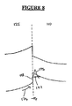
論文「ワイドギャップ半導体高出力デバイスの現在の状況及び将来の展望(Present Status and Future Prospect of Widegap Semiconductor High−Power Devices)」、Japanese Journal of Applied Physics、45(2006)、7565〜7586頁には、従来技術の有用な要約が提示されている。この論文の図6では、極性AlxGa(1−x)N層を極性GaN層上にヘテロエピタキシャル成長させて、電子を閉じ込めるためのポテンシャル井戸を生成する極性GaN−AlxGa(1−x)Nヘテロ構造を開示している。 Papers “Present Status and Future Prospect of Widegap Semiconductor High-Power Devices”, Japan Journal of Apps 6 to 75, 6: 75 A useful summary of the prior art is presented. In FIG. 6 of this paper, a polar Al x Ga (1-x) N layer is heteroepitaxially grown on the polar GaN layer to generate a potential GaN-Al x Ga (1-x) for confining electrons. N heterostructures are disclosed.
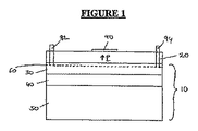
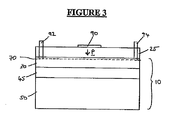
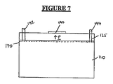
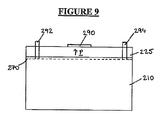
本発明は、2つの材料間に界面を含む電子電界効果デバイスを提供し、この界面は、
少なくとも第1面が結晶真性ダイヤモンドを含む第1ダイヤモンド層と、
第1層の第1面上に配置され、極性がある第2層とによって形成され、
第1層と第2層の間に分極の不連続があり、
主電荷キャリアが存在するバンド内で、第1層と第2層の間にバンドオフセットがあり、その結果、主電荷キャリアが、分極により誘導されたシート電荷と、第1層と記第2層の間の分極の不連続によって形成された電界との複合効果、及びバンドオフセットにより、第1層内のプレーナ領域及び界面の近傍に閉じ込められるようになる。
The present invention provides an electronic field effect device that includes an interface between two materials, the interface comprising:
A first diamond layer having at least a first surface comprising crystal intrinsic diamond;
Disposed on the first surface of the first layer and formed by a second layer having polarity;
There is a discontinuity of polarization between the first layer and the second layer,
Within the band where the main charge carriers are present, there is a band offset between the first layer and the second layer, and as a result, the main charge carriers are the sheet charge induced by polarization, the first layer and the second layer. Due to the combined effect with the electric field formed by the discontinuity of polarization between and the band offset, it becomes confined in the vicinity of the planar region and interface in the first layer.
主電荷キャリアは、デバイスの有用な特性をもたらす。 The main charge carriers provide useful properties of the device.
プレーナ領域は、第3の次元よりもずっと大きい2つの次元を有する領域を含む。 The planar region includes a region having two dimensions that are much larger than the third dimension.
動作中のデバイス内の電荷キャリアは、第1ダイヤモンド層内のプレーナ領域に閉じ込められ、第1層と第2層の間の界面と並行する方向に大部分が移動する。したがって、界面に隣接する第2層内にある転移など、どんな欠陥もデバイスの性能にほとんど影響を及ぼさない。 Charge carriers in the device in operation are confined in the planar region in the first diamond layer and move mostly in a direction parallel to the interface between the first and second layers. Thus, any defect, such as a transition in the second layer adjacent to the interface, has little effect on device performance.
第2層と第1層の間の分極の不連続よって形成される電界によりキャリアが極性材料の方に、したがって界面の方に引き付けられる。 The electric field formed by the polarization discontinuity between the second layer and the first layer attracts carriers towards the polar material and hence towards the interface.
主キャリアは、価電子帯又は伝導帯に存在することができる。そのバンドオフセットは、キャリアが極性材料に入ることを阻止する。 The main carrier can be in the valence band or the conduction band. The band offset prevents the carrier from entering the polar material.
第1層と第2層の少なくとも一方がドープ領域を含むことができる。その場合、ドープ領域はキャリアを供給し、このキャリアはプレーナ領域に移動し、その後そこに閉じ込められることができる。 At least one of the first layer and the second layer may include a doped region. In that case, the doped region supplies carriers which can move to the planar region and then be confined there.
好ましい一実施形態では、第1層又は第2層をドープする代わりに、第2層と第1層の間の分極の不連続によって形成される電界により、価電子帯の最大値がフェルミ準位を横切るようにすることができる。このような場合ではホールが界面で生成され、このホールは、プレーナ領域に移動後にそこに閉じ込められることができるキャリアとして働く。このような場合では、2次元電荷キャリアガスが熱生成キャリアから形成され、第1層にも第2層にもドーパントが不要である。 In one preferred embodiment, instead of doping the first layer or the second layer, the electric field formed by the polarization discontinuity between the second layer and the first layer causes the maximum value of the valence band to be Fermi level. Can be crossed. In such a case, holes are created at the interface, which serve as carriers that can be confined there after moving into the planar region. In such a case, the two-dimensional charge carrier gas is formed from thermally generated carriers and no dopant is required in either the first layer or the second layer.
別法として、第1層又は第2層をドープする代わりに、第2層と第1層の間の分極の不連続によって形成された電界により、伝導帯の最小値がフェルミ準位を横切るようにすることもできる。このような場合では電子が界面で生成され、この電子は、プレーナ領域に移動後そこに閉じ込められることができるキャリアとして働く。このような場合では、2次元電荷キャリアガスが熱生成キャリアから形成され、第1層にも第2層にもドーパントが不要である。 Alternatively, instead of doping the first layer or the second layer, the electric field formed by the polarization discontinuity between the second layer and the first layer causes the conduction band minimum to cross the Fermi level. It can also be. In such a case, electrons are generated at the interface and the electrons act as carriers that can be confined there after moving to the planar region. In such a case, the two-dimensional charge carrier gas is formed from thermally generated carriers and no dopant is required in either the first layer or the second layer.
ドーパントが第1層内に存在する場合、キャリアの移動性を著しく妨げ、それによってデバイスの性能を低下させるドーパントを回避するために、ドーパントは、界面からはプレーナ領域よりも遠く離れており、プレーナ領域から十分に遠い層内にあることが好ましい。したがって、第1層内のドープ領域は、界面から少なくとも2nmのところにあるのが好ましく、界面から少なくとも3nmのところにあるのがより好ましく、界面から少なくとも5nmのところにあるのがより好ましく、界面から少なくとも10nmのところにあるのがより好ましく、界面から少なくとも20nmのところにあるのがより好ましく、界面から少なくとも50nmのところにあるのがより好ましく、界面から少なくとも100nmのところにあるのがより好ましい。界面とドープ領域の間の距離は、2次元電荷キャリアガス中の電荷キャリアの適正な数値の密度を確保するためのドープ層内のドーパント濃度によって影響を受けることがある。ここで「2次元電荷キャリアガス」という用語の意味は、当技術分野で通常理解されているものである。 If the dopant is present in the first layer, the dopant is farther away from the planar region than the planar region to avoid dopants that significantly impede carrier mobility and thereby reduce device performance. It is preferably in a layer sufficiently far from the region. Accordingly, the doped region in the first layer is preferably at least 2 nm from the interface, more preferably at least 3 nm from the interface, and more preferably at least 5 nm from the interface. Is more preferably at least 10 nm from the interface, more preferably at least 20 nm from the interface, more preferably at least 50 nm from the interface, and more preferably at least 100 nm from the interface. . The distance between the interface and the doped region may be affected by the dopant concentration in the doped layer to ensure the proper numerical density of charge carriers in the two-dimensional charge carrier gas. Here, the meaning of the term “two-dimensional charge carrier gas” is commonly understood in the art.
好ましい一実施形態では、第1層は、極性層とドープ領域が真性ダイヤモンドチャネル層によって分離されるように、界面からある距離に配置されたドープ領域を含む真性ダイヤモンド層を含む。真性ダイヤモンド中のドープ領域は、n型領域又はp型領域を含むことができる。ドープ領域がp型領域を含む場合は、電荷キャリアはホールである。このp型ドープ領域は、ホウ素ドープ領域を含むことができる。ドープ領域がn型領域を含む場合は、電荷キャリアは電子である。このn型ドープ領域は、窒素ドープ領域又はリンドープ領域を含むことができる。 In a preferred embodiment, the first layer includes an intrinsic diamond layer that includes a doped region disposed at a distance from the interface such that the polar layer and the doped region are separated by an intrinsic diamond channel layer. The doped region in the intrinsic diamond can include an n-type region or a p-type region. If the doped region includes a p-type region, the charge carriers are holes. The p-type doped region can include a boron doped region. If the doped region includes an n-type region, the charge carriers are electrons. The n-type doped region can include a nitrogen doped region or a phosphorus doped region.
WO2006/117621Alに開示されているMESFETとは異なり、ドープ領域はデルタ層でなくてもよく、また真性ダイヤモンドチャネルに対して原子的に急変しなくてもよい。好ましくは、電荷キャリアの波動関数の二乗係数(|φ(z)|2)はドープ層と重ならないが、大部分が真性層内にある。デバイスのそれぞれの層の厚さは、トランジスタをピンチオフモードで動作できるようにドープ層をゲートで完全に空乏化できなければならないという要件によって制限されることがある。 Unlike the MESFET disclosed in WO 2006/117621 Al, the doped region may not be a delta layer and may not change atomically with respect to the intrinsic diamond channel. Preferably, the square coefficient (| φ (z) | 2 ) of the wave function of the charge carrier does not overlap with the doped layer, but is mostly in the intrinsic layer. The thickness of each layer of the device may be limited by the requirement that the doped layer must be fully depleted at the gate so that the transistor can operate in pinch-off mode.
ドープ領域は、in situドーピング技術(すなわち結晶成長プロセス中のドーピング)によって調製されることが好ましい。具体的には、ドープ領域は、好ましくはホウ素原子をドーパント種として使用して、in situドーピングによって第1ダイヤモンド層内に調製されることが好ましい。 The doped region is preferably prepared by an in situ doping technique (ie doping during the crystal growth process). Specifically, the doped region is preferably prepared in the first diamond layer by in situ doping, preferably using boron atoms as the dopant species.
別法として、ドープ領域は、イオン注入技術によって調製することもできる。具体的には、ドープ領域は、好ましくはホウ素イオン又はホウ素原子のイオン注入によって、第1ダイヤモンド層内に調製することができる。 Alternatively, the doped region can be prepared by ion implantation techniques. Specifically, the doped region can be prepared in the first diamond layer, preferably by ion implantation of boron ions or boron atoms.
界面では、2つの層は、直接接触して間に挟まれる他の材料がないようにすることができる。別法として、2つの層の間に薄いインターフェース材料を設けることもできる。このようなインターフェース材料は、5nm厚未満、より好ましくは2nm厚未満、より好ましくは1nm厚未満の層を形成することが好ましい。インターフェース材料は、0.1nmから5nmの厚さとすることができる。インターフェース材料は、第1層とも第2層とも異なる材料とすることができる。インターフェース材料は、性質が非晶質でも結晶質でもよい。インターフェース材料は、非剛性でコンプライアントな材料が好ましい。インターフェース材料は、原子状水素とすることができる。このような層は、水素化によって形成することができる。インターフェース材料は、絶縁材料であることが好ましい。インターフェース層の一例として0.5nmの非晶質二酸化シリコン(SiO2)がありうる。インターフェース材料は、界面のダングリングボンドを不動態化又は適応させるために設けられることがある。このようなダングリングボンドは、電荷キャリアを捕獲し、電荷キャリア拡散を増大させ、かつ/又は移動度及び伝導度を低減させることができる。 At the interface, the two layers can be in direct contact with no other material sandwiched between them. Alternatively, a thin interface material can be provided between the two layers. Such an interface material preferably forms a layer less than 5 nm thick, more preferably less than 2 nm thick, more preferably less than 1 nm thick. The interface material can be 0.1 nm to 5 nm thick. The interface material can be a different material from both the first layer and the second layer. The interface material may be amorphous or crystalline in nature. The interface material is preferably a non-rigid and compliant material. The interface material can be atomic hydrogen. Such a layer can be formed by hydrogenation. The interface material is preferably an insulating material. An example of the interface layer may be 0.5 nm of amorphous silicon dioxide (SiO 2 ). An interface material may be provided to passivate or adapt the interface dangling bonds. Such dangling bonds can trap charge carriers, increase charge carrier diffusion, and / or reduce mobility and conductivity.
第1ダイヤモンド層は、好ましくは非極性の、より好ましくは単結晶ダイヤモンドの、より好ましくは単結晶CVDダイヤモンドの、より好ましくはWO01/96633及びWO01/96634に開示されたものと一致する材料特性を有する単結晶CVDダイヤモンドの、広バンドギャップ半導体材料である。 The first diamond layer preferably has material properties consistent with those disclosed in non-polar, more preferably single crystal diamond, more preferably single crystal CVD diamond, more preferably WO 01/96633 and WO 01/96634. It is a wide band gap semiconductor material of single crystal CVD diamond.
第2層は、好ましくは第1層よりも広いバンドギャップを有し、より好ましくはそのウルツ鉱相中にAlNを含む。代替の第2層は、AlxGa(1−x)Nを含むことができる。ここでx≧0.8である。 The second layer preferably has a wider band gap than the first layer, and more preferably comprises AlN in its wurtzite phase. An alternative second layer can include Al x Ga (1-x) N. Here, x ≧ 0.8.
このようなデバイス中には、電子及びホールの2種類の可能な電荷キャリアがあるので、デバイスは2つの別個の形を取ることができる。 In such a device, there are two possible charge carriers, electrons and holes, so the device can take two distinct forms.
主電荷キャリアの種類がホールである場合は、ホールは、極性層によって形成される分極電界と、第1層と第2層の間の価電子帯オフセットとの複合効果によってプレーナ領域に閉じ込められ、分極電界は分極ベクトルを有し、これは、界面から離れる方向に向くとともに、界面に向かうホールを引き付けることになり、価電子帯オフセットは、ホールが極性層に入るのを阻止するポテンシャルエネルギー障壁を形成し、第2層の価電子帯の最大値は、第1層の価電子帯の最大値よりも小さい。 When the main charge carrier type is a hole, the hole is confined in the planar region by the combined effect of the polarization electric field formed by the polar layer and the valence band offset between the first and second layers, The polarization electric field has a polarization vector that points away from the interface and attracts holes toward the interface, and the valence band offset creates a potential energy barrier that prevents holes from entering the polar layer. The maximum value of the valence band of the second layer is smaller than the maximum value of the valence band of the first layer.
主電荷キャリアの種類が電子である場合は、電子は、極性層によって形成される分極電界と、第1層と第2層の間の伝導帯オフセットとの複合効果によってプレーナ領域に閉じ込められ、分極電界は分極ベクトルを有し、これは、界面の方に向くとともに、界面に向かう電子を引き付けることになり、伝導帯オフセットは、電子が極性層に入るのを阻止するポテンシャルエネルギー障壁を形成し、第2層の伝導帯の最小値は、第1層の価電子帯の最小値よりも大きい。 When the main charge carrier type is an electron, the electron is confined in the planar region by the combined effect of the polarization electric field formed by the polar layer and the conduction band offset between the first layer and the second layer. The electric field has a polarization vector, which is directed towards the interface and attracts electrons towards the interface, and the conduction band offset forms a potential energy barrier that prevents the electrons from entering the polar layer, The minimum value of the conduction band of the second layer is larger than the minimum value of the valence band of the first layer.
本発明の好ましい一実施形態では、第2層のバンドギャップは第1層よりも大きい。 In a preferred embodiment of the present invention, the band gap of the second layer is larger than that of the first layer.
別の好ましい一実施形態では、第2層のバンドギャップは第1層よりも大きく、伝導帯と価電子帯のバンドオフセットは、電子もホールも極性層に入るのを阻止するものである。すなわち、第2層の価電子帯の最大値は第1層の価電子帯の最大値よりも小さく、第2層の伝導帯の最小値は第1層の伝導帯の最小値よりも大きい。この状態は、「タイプIバンドオフセット」として知られている。 In another preferred embodiment, the band gap of the second layer is larger than that of the first layer, and the band offset between the conduction band and the valence band prevents electrons and holes from entering the polar layer. That is, the maximum value of the valence band of the second layer is smaller than the maximum value of the valence band of the first layer, and the minimum value of the conduction band of the second layer is larger than the minimum value of the conduction band of the first layer. This condition is known as “Type I Band Offset”.
主キャリアがホールである場合は、第1層から第2層まで移動する価電子帯オフセットは負であり、そのモジュラスは、好ましくは0.05eVよりも大きく、より好ましくは0.1eVよりも大きく、より好ましくは0.15eVよりも大きく、より好ましくは0.2eVよりも大きく、より好ましくは0.3eVよりも大きく、より好ましくは0.4eVよりも大きく、より好ましくは0.5eVよりも大きい。 When the main carrier is a hole, the valence band offset moving from the first layer to the second layer is negative, and its modulus is preferably greater than 0.05 eV, more preferably greater than 0.1 eV. More preferably greater than 0.15 eV, more preferably greater than 0.2 eV, more preferably greater than 0.3 eV, more preferably greater than 0.4 eV, more preferably greater than 0.5 eV. .
第1層の真性領域内にホールが保持されるようにデバイスが適切に設計されるならば、原理上は、適用可能な価電子帯オフセットのモジュラス(又は最大の負の値)に上限はない。現在の材料可用性では約2eVという実際的な限界があるが、これは本発明の範囲を限定するものではない。 In principle, there is no upper limit to the applicable valence band offset modulus (or maximum negative value) if the device is properly designed to hold holes in the intrinsic region of the first layer. . Current material availability has a practical limit of about 2 eV, but this does not limit the scope of the invention.
主キャリアが電子である場合は、第1層から第2層まで移動する伝導帯オフセットは正であり、好ましくは+0.05eVよりも大きく、より好ましくは+0.1eVよりも大きく、より好ましくは+0.15eVよりも大きく、より好ましくは+0.2eVよりも大きく、より好ましくは+0.3eVよりも大きく、より好ましくは+0.4eVよりも大きく、より好ましくは+0.5eVよりも大きい。 When the main carrier is an electron, the conduction band offset moving from the first layer to the second layer is positive, preferably greater than +0.05 eV, more preferably greater than +0.1 eV, more preferably +0. Greater than .15 eV, more preferably greater than +0.2 eV, more preferably greater than +0.3 eV, more preferably greater than +0.4 eV, and more preferably greater than +0.5 eV.
第1層の真性領域内に電子が保持されるようにデバイスが適切に設計されるならば、原理上は、適用可能な伝導帯オフセットのモジュラス(又は最大の正の値)に上限はない。現在の材料可用性では約2eVという実際的な限界があるが、これは本発明の範囲を限定するものではない。 In principle, there is no upper limit to the applicable conduction band offset modulus (or maximum positive value) if the device is properly designed to retain electrons in the intrinsic region of the first layer. Current material availability has a practical limit of about 2 eV, but this does not limit the scope of the invention.
第2層のバンドギャップが第1層のバンドギャップよりも大きい場合は、好ましくは0.1eVだけ大きく、より好ましくは0.2eVだけ大きく、より好ましくは0.3eVだけ大きく、より好ましくは0.4eVだけ大きく、より好ましくは0.6eVだけ大きく、より好ましくは0.8eVだけ大きく、より好ましくは1.0eVだけ大きく、より好ましくは1.2eVだけ大きい。本発明の目的のために、ダイヤモンドのバンドギャップは5.47eVに選ばれる。 When the band gap of the second layer is larger than the band gap of the first layer, it is preferably larger by 0.1 eV, more preferably larger by 0.2 eV, more preferably larger by 0.3 eV, more preferably 0. It is larger by 4 eV, more preferably by 0.6 eV, more preferably by 0.8 eV, more preferably by 1.0 eV, more preferably by 1.2 eV. For the purposes of the present invention, the band gap of diamond is chosen to be 5.47 eV.
第1層の真性領域内にキャリアが保持されるようにデバイスが適切に設計されるならば、原理上は、第2層のバンドギャップに上限はない。現在の材料可用性では約9eVという実際的な限界があるが、これは本発明の範囲を限定するものではない。 In principle, there is no upper limit on the band gap of the second layer if the device is properly designed to retain carriers in the intrinsic region of the first layer. Current material availability has a practical limit of about 9 eV, but this does not limit the scope of the invention.
デバイスは、3端子デバイスを含むことができる。好ましくは、デバイスは電界効果トランジスタ(FET)を含む。このデバイスでは、極性層が空間を分離することになり、またプレーナ領域内に電荷キャリアを閉じ込めることになり、これはデバイスの性能の向上につながるという事実にかんがみて、このデバイスを本明細書では「分極強化(Polarization Enhanced)FET」又はPE−FETと呼ぶものとする。PE−FETは、トランジスタ構造を画定するために適切な電気接点を含むことができる。この電気接点は、ゲート、ソース及びドレインを含むことができる。 The device can include a three terminal device. Preferably, the device comprises a field effect transistor (FET). In this device, in view of the fact that the polar layer will separate the space and will confine charge carriers in the planar region, which will lead to improved device performance, this device will be referred to herein. It shall be called “Polarization Enhanced FET” or PE-FET. The PE-FET can include appropriate electrical contacts to define the transistor structure. The electrical contacts can include a gate, a source, and a drain.
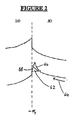
非極性真性ダイヤモンド層と第2極性層の間の分極の不連続が、分極により誘導するシート電荷σp=−(Pn)を2つの層の間の界面に生成する。ここでPnは、2つの層の間の界面に対して直角の極性層内の分極成分である。Pnは、それが2つの層の間の界面から離れる向きのときに正と定義される。このようなシート電荷は、ダイヤモンド層内でも第2極性層内でもかなりの強度の電界をもたらす。このシート電荷は、第2極性層内の、極性材料の結晶構造によって固定されている原子双極子が現れたものであるので移動性がない。バンドオフセットは、ポテンシャル障壁として働く。電界と結合したこのポテンシャル障壁は、キャリアを引き付けるのに使用できる三角形のポテンシャル井戸になり、その結果、界面に近いダイヤモンド層の領域内に高度に閉じ込められた2次元の電子ガス又はホールガスが生じる。 The polarization discontinuity between the nonpolar intrinsic diamond layer and the second polar layer generates a sheet charge σ p = − (P n ) induced by polarization at the interface between the two layers. Where P n is the polarization component in the polar layer perpendicular to the interface between the two layers. P n is defined as positive when it is oriented away from the interface between the two layers. Such sheet charge results in a strong electric field both in the diamond layer and in the second polar layer. This sheet charge is not mobile because it is the manifestation of atomic dipoles fixed by the crystal structure of the polar material in the second polar layer. The band offset acts as a potential barrier. This potential barrier combined with an electric field results in a triangular potential well that can be used to attract carriers, resulting in a two-dimensional electron or hole gas that is highly confined in the region of the diamond layer near the interface. .
閉じ込められた2次元電荷キャリアガスの広がりは、プレーナ領域と呼ばれる領域を画定する。この領域は、大きい寸法にわたって、例えば1μmよりも大きい、より好ましくは10μmよりも大きい、より好ましくは100μmよりも大きい、より好ましくは1mmよりも大きい寸法にわたって必ずしも平坦ではないが、第1層と第2層の間の界面のどんな大規模の湾曲部とも合致する。プレーナ領域内で相対的に鋭いフィーチャになるはずの、第1層と第2層の間の界面内の鋭いフィーチャは望ましくなく、電荷キャリアの拡散を引き起こすことによってデバイスの性能を低下させることがある。これは、第1層と第2層の間の界面を形成する面の慎重な調製によって制御される。具体的には、第1層の第1面は、好ましくは10nm未満の二乗平均粗度Rq、好ましくは5nm未満のRq、好ましくは3nm未満のRq、好ましくは2nm未満のRq、好ましくは1nm未満のRq、好ましくは0.5nm未満のRq、好ましくは0.3nm未満のRq、好ましくは0.2nm未満のRq、好ましくは0.1nm未満のRqを有する。さらに、第1層に面する第2層の面は、好ましくは10nm未満のRq、好ましくは5nm未満のRq、好ましくは3nm未満のRq、好ましくは2nm未満のRq、好ましくは1nm未満のRq、好ましくは0.5nm未満のRq、好ましくは0.3nm未満のRq、好ましくは0.2nm未満のRq、好ましくは0.1nm未満のRqを有する。 The spread of the confined two-dimensional charge carrier gas defines a region called the planar region. This region is not necessarily flat over a large dimension, for example greater than 1 μm, more preferably greater than 10 μm, more preferably greater than 100 μm, more preferably greater than 1 mm, but the first layer and the first layer Matches any large bend at the interface between the two layers. Sharp features in the interface between the first and second layers, which should be relatively sharp features in the planar region, are undesirable and can degrade device performance by causing charge carrier diffusion. . This is controlled by careful preparation of the surface that forms the interface between the first and second layers. Specifically, the first surface of the first layer preferably has a root mean square roughness R q of less than 10 nm, preferably R q of less than 5 nm, preferably R q of less than 3 nm, preferably R q of less than 2 nm, preferably it has less than 1 nm R q, preferably less than 0.5 nm R q, preferably less than 0.3 nm R q, preferably less than 0.2 nm R q, and preferably less than 0.1 nm R q. Furthermore, the surface of the second layer facing the first layer is preferably less than 10 nm R q , preferably less than 5 nm R q , preferably less than 3 nm R q , preferably less than 2 nm R q , preferably 1 nm having less than R q, preferably less than 0.5 nm R q, preferably less than 0.3 nm R q, preferably less than 0.2 nm R q, preferably less than 0.1 nm R q.
第1層は、その第1面の領域内の転移密度が低いことが望ましい。具体的には、第1層の第1面を破壊する転移の密度は、0.014cm2よりも大きい、好ましくは0.1cm2よりも大きい、好ましくは0.25cm2よりも大きい、好ましくは0.5cm2よりも大きい、好ましくは1cm2よりも大きい、好ましくは2cm2よりも大きい面積にわたって測定されて、400cm−2未満であり、好ましくは300cm−2未満であり、好ましくは200cm−2未満であり、好ましくは100cm−2未満であることが望ましい。 The first layer preferably has a low transition density in the region of the first surface. Specifically, the density of the transition to destroy the first surface of the first layer is greater than 0.014 cm 2, preferably greater than 0.1 cm 2, preferably greater than 0.25 cm 2, preferably greater than 0.5 cm 2, preferably greater than 1 cm 2, preferably measured over an area larger than 2 cm 2, less than 400 cm -2, preferably less than 300 cm -2, preferably 200 cm -2 It is desirable that it is less than 100 cm −2 .
転移密度が低いダイヤモンド及びダイヤモンド面を調製し特徴付ける方法が、WO01/96633、WO01/96634、WO2004/027123、及び同時係属出願PCT/IB2006/003531の従来技術に報告されている。転移密度を特徴付ける好ましい方法は、「暴露プラズマエッチング(revealing plasma etch)」を使用するもの、及びX線トポグラフィを使用するものである。 Methods for preparing and characterizing diamonds and diamond surfaces with low transition density have been reported in the prior art of WO 01/96633, WO 01/96634, WO 2004/027123, and co-pending application PCT / IB2006 / 003531. Preferred methods for characterizing the transition density are those using “revealing plasma etch” and using X-ray topography.
第1層の表面は、成長させたままの面の成長後機械加工によって生じる損傷が、少なくとも1nm、好ましくは少なくとも2nm、好ましくは少なくとも5nm、好ましくは少なくとも10nm、好ましくは少なくとも20nm、好ましくは少なくとも50nm、好ましくは少なくとも100nm、好ましくは少なくとも200nm、好ましくは少なくとも500nmの深さまで実質的にないことがさらに望ましい。微小破断並びに機械的に生成された点欠陥及び拡張欠陥を含む、このような損傷が存在することが、キャリアの拡散及び捕獲、局部電界の乱れ、及び絶縁破壊電界の低下を経て、デバイスの性能に有害な影響を及ぼしうる。 The surface of the first layer has at least 1 nm, preferably at least 2 nm, preferably at least 5 nm, preferably at least 10 nm, preferably at least 20 nm, preferably at least 50 nm in damage caused by post-growth machining of the as-grown surface. More desirably, it is substantially free to a depth of preferably at least 100 nm, preferably at least 200 nm, preferably at least 500 nm. The presence of such damage, including microfracture and mechanically generated point and extended defects, can lead to device performance via carrier diffusion and trapping, local field disturbances, and breakdown breakdown. May have detrimental effects on
ダイヤモンドの場合、特に単結晶CVDダイヤモンドの場合には、このような欠陥は、従来のラッピング技術及びポリシング技術の使用など、成長させたままの面の機械加工によって材料中に導入される可能性がある。これらの問題は、ダイヤモンドの硬くて砕けやすい性質と、利用可能な化学的及び物理的エッチング工程の数を制限するその化学的抵抗性を考えると、特にダイヤモンドに関係する。粗度を小さくするように電子面を加工する要件と、表面損傷を少なくするように電子面を加工する要件とは全く異なる。これら両方のフィーチャを示す電子面の調製は、本発明の別の一態様である。 In the case of diamond, particularly in the case of single crystal CVD diamond, such defects can be introduced into the material by machining the as-grown surface, such as using conventional lapping and polishing techniques. is there. These problems are particularly relevant for diamonds given the hard and friable nature of diamonds and their chemical resistance which limits the number of chemical and physical etching steps available. The requirement for processing the electronic surface to reduce the roughness is completely different from the requirement for processing the electronic surface to reduce surface damage. The preparation of an electronic surface exhibiting both these features is another aspect of the present invention.
一般に、成長中に生じうる非平面フィーチャが存在することにより、成長させたままの状態の単結晶CVDダイヤモンドの厚い層は、第1層として使用するのに適さず、その表面は、第1面として使用するのに適さない。反対に、電子面を上に調製すべきダイヤモンド層は、加工及び取扱いに十分なほどに剛性で堅牢である必要があり、したがって、電子デバイスの製造は通常、厚いダイヤモンド層から開始する。厚いダイヤモンド層の成長させたままの面から適切なダイヤモンド面を作製する方法がいくつかあり、成長させたままの面の加工工程はその方法に含まれる。本発明との関連では、単結晶CVD層は、その厚さが20μmを越える場合に厚いとみなす。 In general, due to the presence of non-planar features that can occur during growth, a thick layer of as-grown single crystal CVD diamond is not suitable for use as the first layer, and its surface is the first surface. Not suitable for use as. Conversely, the diamond layer to be prepared with the electronic surface up needs to be rigid and robust enough to be processed and handled, and thus the manufacture of electronic devices usually starts with a thick diamond layer. There are several methods for producing a suitable diamond surface from the as-grown surface of the thick diamond layer, and the process of processing the as-grown surface is included in the method. In the context of the present invention, a single crystal CVD layer is considered thick if its thickness exceeds 20 μm.
まず、厚いダイヤモンド層上に、例えば暴露エッチングからのフィードバックを使用して表面損傷を最小にするように最適化された機械的ラッピング加工及びポリシング加工を用いて、1つの面を調製することができる。このような技術は、例えばWO01/96633及びWO01/96634に記載されている。このような面は、低い損傷レベルを有しうるが、デバイスから十二分な性能を得るのに十分なほどには損傷がなくなりそうにない。 First, a single surface can be prepared on a thick diamond layer using a mechanical lapping and polishing process optimized to minimize surface damage, for example using feedback from exposure etching. . Such techniques are described, for example, in WO 01/96633 and WO 01/96634. Such a surface may have a low damage level, but is unlikely to be damaged enough to obtain sufficient performance from the device.
第1面は、上記の方法を用いることによって、化学エッチング、或いはイオンビームミリング、プラズマエッチング又はレーザアブレーションなどの他の形式のエッチングと、より好ましくはプラズマエッチングとを含む別の加工段階を用いることによって、加工された面から、好ましくは機械的に加工された面から、好ましくは表面損傷が最小になるようにそれ自体最適化されて機械的に調製された面から調製することができる。エッチング段階では、少なくとも10nm、好ましくは少なくとも100nm、より好ましくは少なくとも1μm、より好ましくは少なくとも2μm、より好ましくは少なくとも5μm、より好ましくは少なくとも10μmを除去するのが好ましい。このエッチング段階では、100μm未満、好ましくは50μm未満、好ましくは20μm未満を除去するのが好ましい。さらに加工されたこの面は、10nm未満のRq、好ましくは5nm未満のRq、好ましくは3nm未満のRq、好ましくは2nm未満のRq、好ましくは1nm未満のRq、好ましくは0.5nm未満のRq、好ましくは0.3nm未満のRq、好ましくは0.2nm未満のRq、好ましくは0.1nm未満のRqを有することが好ましい。 The first surface uses another process step, including chemical etching, or other types of etching such as ion beam milling, plasma etching or laser ablation, and more preferably plasma etching, by using the method described above. Can be prepared from a machined surface, preferably from a machined surface, preferably from a surface that is itself optimized and mechanically prepared to minimize surface damage. In the etching step, it is preferable to remove at least 10 nm, preferably at least 100 nm, more preferably at least 1 μm, more preferably at least 2 μm, more preferably at least 5 μm, more preferably at least 10 μm. In this etching step, it is preferable to remove less than 100 μm, preferably less than 50 μm, preferably less than 20 μm. This further processed surface is less than 10 nm R q , preferably less than 5 nm R q , preferably less than 3 nm R q , preferably less than 2 nm R q , preferably less than 1 nm R q , preferably 0. 5nm less than R q, preferably less than 0.3 nm R q, preferably less than 0.2 nm R q, preferably preferably has a R q of less than 0.1 nm.
別法として、第1面は、上記の方法を用いることによって、加工された面から、好ましくは機械的に加工された面から、好ましくは表面損傷が最小になるようにそれ自体最適化されて機械的に調製された面から調製することができ、或いは、上述したものなどエッチングされた面から、好ましくはCVDプロセスを用いて別の薄いダイヤモンドの層をその面の上に成長させることによって調製することができる。別の薄いダイヤモンド層の堆積の前に、加工された面は、10nm未満のRq、好ましくは5nm未満のRq、好ましくは3nm未満のRq、好ましくは2nm未満のRq、好ましくは1nm未満のRq、好ましくは0.5nm未満のRq、好ましくは0.3nm未満のRq、好ましくは0.2nm未満のRq、好ましくは0.1nm未満のRqを有する。 Alternatively, the first surface is itself optimized by using the method described above from a machined surface, preferably from a mechanically machined surface, preferably with minimal surface damage. Can be prepared from a mechanically prepared surface, or from an etched surface such as those described above, preferably by growing another thin diamond layer on the surface using a CVD process can do. Prior to the deposition of another thin diamond layer, processed surfaces, 10 nm less than R q, preferably less than 5 nm R q, preferably less than 3 nm R q, preferably less than 2 nm R q, preferably 1nm having less than R q, preferably less than 0.5 nm R q, preferably less than 0.3 nm R q, preferably less than 0.2 nm R q, preferably less than 0.1 nm R q.
このようなダイヤモンド層は、CVD合成によって成長させるのが好ましく、巨視的成長段階の形成を制限するために薄くする。前もって調製された面の上に成長させるこの層の厚さは、20μm未満、好ましくは10μm未満、好ましくは1μm未満、好ましくは100nm未満、好ましくは50nm未満、好ましくは20nm未満、好ましくは10nm未満である。その後、この薄い層の面は、その成長させたままの状態で第1面として使用される。 Such diamond layers are preferably grown by CVD synthesis and are thinned to limit the formation of macroscopic growth stages. The thickness of this layer grown on the previously prepared surface is less than 20 μm, preferably less than 10 μm, preferably less than 1 μm, preferably less than 100 nm, preferably less than 50 nm, preferably less than 20 nm, preferably less than 10 nm. is there. The thin layer surface is then used as the first surface in its grown state.
このような薄い層は、単層成長技術と、表面ステップの伝搬を制御するための軸外表面の使用とを含むいくつかの技術を用いて調製することができる。 Such thin layers can be prepared using a number of techniques including single layer growth techniques and the use of off-axis surfaces to control the propagation of surface steps.
この面は、その上にホモエピタキシャルCVDダイヤモンド成長が最も容易に実施される面であるので、{001}面のものに近いミラー指数を有するのが好ましい。或いは、この面は{111}面のものに近いミラー指数を有することも、このような面がAlN層の堆積に最も適していることが分かっているので、可能である。この面に対する垂線は、{001}面又は{111}面に対する垂線の、好ましくは0°と約5°の間、好ましくは約0.5°と約1°の間にある。面が{001}面に近い場合、この面に対する垂線は、{001}面の極と、隣接する{101}面の極とを通る大円の約10°以内にあるのが好ましい。 Since this surface is the surface on which homoepitaxial CVD diamond growth is most easily performed, it preferably has a Miller index close to that of the {001} surface. Alternatively, it is possible that this plane has a Miller index close to that of the {111} plane since such a plane has been found to be most suitable for the deposition of an AlN layer. The normal to this plane is preferably between 0 ° and about 5 °, preferably between about 0.5 ° and about 1 ° of the normal to the {001} or {111} plane. When the surface is close to the {001} plane, the normal to this plane is preferably within about 10 ° of a great circle passing through the pole of the {001} plane and the adjacent pole of the {101} plane.
このような層は、好ましくは高純度の真性ダイヤモンドを含み、より好ましくは、WO01/96633及びWO01/96634に開示されたものと合致する材料特性を有する高純度の真性ダイヤモンドを含む。 Such a layer preferably comprises high purity intrinsic diamond, and more preferably comprises high purity intrinsic diamond having material properties consistent with those disclosed in WO01 / 96633 and WO01 / 96634.
この成長させたままの薄い層の表面が第1面を形成し、好ましくは10nm未満のRq、好ましくは10nm未満のRq、好ましくは5nm未満のRq、好ましくは3nm未満のRq、好ましくは2nm未満のRq、好ましくは1nm未満のRq、好ましくは0.5nm未満のRq、好ましくは0.3nm未満のRq、好ましくは0.2nm未満のRq、好ましくは0.1nm未満のRqを有する。すなわち、この表面は非常に小さい表面粗度を有し、さらに加工損傷がない。 The surface of this as-grown thin layer forms the first surface, preferably less than 10 nm R q , preferably less than 10 nm R q , preferably less than 5 nm R q , preferably less than 3 nm R q , Preferably R q less than 2 nm, preferably less than 1 nm R q , preferably less than 0.5 nm R q , preferably less than 0.3 nm R q , preferably less than 0.2 nm R q , preferably 0. having a R q of less than 1 nm. That is, this surface has a very small surface roughness and is not damaged by processing.
ダイヤモンドの場合では、この層を上に成長させることができる調製された面は、どんな形のダイヤモンドでもよいが、CVD合成ダイヤモンドが好ましく、また第1層がドープ層を含む場合は、そのドープ層がすでにあるCVD合成ダイヤモンドがより好ましく、このドープ層がすでにCVD合成によって形成されているのがより好ましい。 In the case of diamond, the prepared surface on which this layer can be grown can be any form of diamond, but CVD synthetic diamond is preferred, and if the first layer includes a doped layer, the doped layer Is more preferred, and it is more preferred that this doped layer is already formed by CVD synthesis.
このドープ層は、真性半導体層の最終合成の前に加工される面を形成することができる。 This doped layer can form a surface that is processed prior to final synthesis of the intrinsic semiconductor layer.
極性層は焦電材料又は圧電材料を含むことができる。しかし、極性界の主要源は、たとえ圧電効果がまた存在しても、極性層の焦電特性によるものである。極性層はAlNを含むことができ、これは、Eg=6.2eVのバンドギャップエネルギーを有し、ダイヤモンド層とAlN層の間の界面に1MVcm−1よりもずっと大きい電界強度をもたらす。AlNは、広いバンドギャップを有し、市販で容易に入手でき、大きな自発分極、良好な熱特性並びに堅牢性を有するという利点を提供する。 The polar layer can comprise a pyroelectric material or a piezoelectric material. However, the main source of the polar field is due to the pyroelectric properties of the polar layer, even if the piezoelectric effect is also present. Polar layer can include AlN, which has a band gap energy of Eg = 6.2 eV, resulting in much greater field strength than 1 MV cm -1 at the interface between the diamond layer and the AlN layer. AlN has the advantage of having a wide band gap, readily available in the market, and having large spontaneous polarization, good thermal properties and robustness.
第2極性層は、2つ以上の極性層で形成された複合層を含むことができる。このような複合第2極性層を形成すると、2次元キャリアガスの密度をより精密に制御する代替方法が得られる。極性層は、AlN又はAlGaNなどのIII−V極性材料が好ましい。例えば、第2層は、AlGaN層が上に形成されたAlN層を含む複合層を含むことができる。 The second polar layer can include a composite layer formed of two or more polar layers. Forming such a composite second polar layer provides an alternative method for more precisely controlling the density of the two-dimensional carrier gas. The polar layer is preferably a III-V polar material such as AlN or AlGaN. For example, the second layer can include a composite layer including an AlN layer with an AlGaN layer formed thereon.
極性層とすべき材料については、その応力が加わらない状態で、結晶点群が次の、1、2、m、mm2、3、3m、4、4mm、6又は6mmのうちの1つでなければならない。ここで記号は、ヘルマン−モーガンの記号である。好ましい材料のAlNは、点群6mmを有する。 For the material to be the polar layer, the crystal point group must be one of the following 1, 2, m, mm2, 3, 3m, 4, 4mm, 6 or 6mm with no stress applied. I must. Here, the symbol is a Hermann-Morgan symbol. A preferred material, AlN, has a point group of 6 mm.
別法として、圧電結晶点群の1つを有する極性ではない材料が、応力が加えられた状態でそれを堆積させることによって極性にすることができる。該当する圧電結晶点群は、ヘルマン−モーガンの記号で

である。
Alternatively, a non-polar material having one of the piezoelectric crystal point groups can be made polar by depositing it under stress. The corresponding piezoelectric crystal point group is the Hermann-Morgan symbol.
It is.
極性材料の分極ベクトルPの方向は、その結晶構造の1つの特性である。窒化アルミニウムを一例として用いると、[0001]の結晶方向は、Al−N結合の一組と平行であり、Al原子からN原子の方に向くと定義される。Al原子はわずかに正に帯電し、窒素原子はわずかに負に帯電し、原子の空間配列により自発分極Pが形成される。A1Nでは、Pは常に
方向にある。
The direction of the polarization vector P of a polar material is one characteristic of its crystal structure. Using aluminum nitride as an example, the crystal direction of [0001] is defined to be parallel to one set of Al—N bonds and from the Al atom to the N atom. Al atoms are slightly positively charged, nitrogen atoms are slightly negatively charged, and spontaneous polarization P is formed by the spatial arrangement of the atoms. In A1N, P is always
In the direction.
バンドオフセット及びバンドギャップに対する必要な基準に適合する極性層の候補材料の特定は、特に第1層がすでにダイヤモンドのような広バンドギャップ材料である場合には、簡単なことではない。可能性がある候補材料には、
応力が加えられた状態にある水晶の形のSiO2(点群32)、及び
六方晶の窒化ホウ素(点群6mm)が含まれる。
The identification of polar layer candidate materials that meet the necessary criteria for band offset and band gap is not straightforward, especially if the first layer is already a wide band gap material such as diamond. Possible candidate materials include:
It includes SiO 2 (point group 32) in the form of crystal in a stressed state, and hexagonal boron nitride (point group 6 mm).
本発明はまた、
少なくとも第1面が結晶真性ダイヤモンドを含む第1ダイヤモンド層を設けるステップと、
極性があり、第1層の第1面上に配置される第2層を設けるステップとによって、第1層と第2層の間に界面を形成するステップを含む、電子電界効果デバイスを形成する方法であって、
第1層と第2層の間に分極の不連続があり、
主電荷キャリアが存在するバンド内で、第1層と第2層の間にバンドオフセットがあり、その結果、主電荷キャリアが、分極により誘導されたシート電荷と、第1層と第2層の間の分極の不連続によって形成された電界との複合効果、及びバンドオフセットにより、第1層内のプレーナ領域及び界面の近傍に閉じ込められるようになる方法も提供する。
The present invention also provides
Providing a first diamond layer having at least a first surface comprising crystalline intrinsic diamond;
Providing a second layer that is polar and disposed on a first surface of the first layer to form an electronic field effect device comprising forming an interface between the first layer and the second layer A method,
There is a discontinuity of polarization between the first layer and the second layer,
Within the band where the main charge carriers are present, there is a band offset between the first layer and the second layer, so that the main charge carriers are separated from the sheet charge induced by polarization, the first layer and the second layer. There is also provided a method of becoming confined in the vicinity of the planar region and interface in the first layer due to the combined effect with the electric field formed by the discontinuity of polarization between and the band offset.
概念的に、このデバイスは第1層及び第2層を含むが、これは製造の順序を制限するものではない。例えば、第2層を既存の第1層の上に、例えばPVDプロセス又はCVDプロセスによって形成することができ、或いは第1層を既存の第2層の上に、例えばPVDプロセス又はCVDプロセスによって形成することができ、或いは2つの層を完全に別々に形成し、その後で接合することもできる。 Conceptually, the device includes a first layer and a second layer, but this does not limit the order of manufacture. For example, the second layer can be formed on an existing first layer, for example by a PVD process or a CVD process, or the first layer can be formed on an existing second layer, for example by a PVD process or a CVD process. Alternatively, the two layers can be formed completely separately and then joined.
ヘテロ構造及び変調ドーピングなど、他のシステムで使用される電荷キャリア閉じ込めの従来の方法は、ダイヤモンドでは実際的ではない。すなわち、ダイヤモンドの極端な電子的諸特性を活用するデバイスの開発に対する相当な関心にもかかわらず、他の半導体システムにおいて従来技術によって教示される代替選択肢がダイヤモンドには適用可能ではないために、すべての努力が、デルタドープ層などダイヤモンド中で制御される構造に集中されてきた。しかし、本発明の方法は、簡単なダイヤモンド構造を他の極性材料と組み合わせて用い、非常に移動性のある2Dキャリアガスをダイヤモンド中に形成することを実現する。 Conventional methods of charge carrier confinement used in other systems, such as heterostructures and modulation doping, are not practical with diamond. In other words, despite the considerable interest in developing devices that take advantage of the extreme electronic properties of diamond, all alternatives taught by the prior art in other semiconductor systems are not applicable to diamond, Efforts have been focused on structures controlled in diamond, such as delta doped layers. However, the method of the present invention achieves the formation of a very mobile 2D carrier gas in diamond using a simple diamond structure in combination with other polar materials.
ダイヤモンドに関する特別な問題は、表面終端の問題である。ダイヤモンドの電子親和力は、例えば水素又は酸素でダイヤモンド表面を終端することによって、清浄なダイヤモンド表面の電子親和力に対して変更できることがよく知られている。2つの異種材料間のバンドオフセットの位置が、それらの材料の電子親和性の関数になりうるので(当技術分野で「アンダーソンの規則」として知られている)、適切に終端されたダイヤモンド表面を使用すると、2Dガス密度、及びキャリア波動関数の空間プロファイルなどのパラメータを制御することによって、デバイス性能を改善するようにバンドオフセットを制御するために使用することができる。例えば、電子親和性は、水素終端された表面が、終端されていない表面と比較して低下すると考えられる。すなわち、理想的な構造では、例えば、第1ダイヤモンド層からAlNの第2極性層に直に達することができるが、実際には、この界面は、H、O、F、OH(これらのそれぞれの様々な同位体代替物を含む)など他の化学種の部分単層、単層、又は複数の単層を含むことがある。ダイヤモンド層と極性層の間の伝導帯オフセット及び価電子帯オフセットを制御するために、ダイヤモンド層を非炭素化学種で意図的に終端する、或いは別の方法でそのような化学種を界面に挿入することが望ましいことがある。この技術は、界面全体にわたる格子連続性についての要件がないので、特に適切である。前述のように、どんなダングリングボンドも不動態化させるように、非晶質層又は原子水素層が界面層に設けられることがある。このような原子水素層は、水素化によって設けることができる。 A special problem with diamond is the problem of surface termination. It is well known that the electron affinity of diamond can be changed relative to that of a clean diamond surface, for example by terminating the diamond surface with hydrogen or oxygen. Since the position of the band offset between two dissimilar materials can be a function of the electron affinity of those materials (known in the art as the “Anderson rule”), a properly terminated diamond surface When used, it can be used to control the band offset to improve device performance by controlling parameters such as 2D gas density and the spatial profile of the carrier wave function. For example, the electron affinity is thought to be reduced for hydrogen-terminated surfaces compared to unterminated surfaces. That is, in an ideal structure, for example, it is possible to reach the second polar layer of AlN directly from the first diamond layer, but in practice, this interface is H, O, F, OH (each of these May include partial monolayers, monolayers, or multiple monolayers of other chemical species (including various isotope substitutes). In order to control the conduction band offset and valence band offset between the diamond layer and the polar layer, the diamond layer is intentionally terminated with a non-carbon species or otherwise inserted into the interface. It may be desirable to do so. This technique is particularly suitable because there is no requirement for lattice continuity across the interface. As previously mentioned, an amorphous or atomic hydrogen layer may be provided in the interfacial layer to passivate any dangling bonds. Such an atomic hydrogen layer can be provided by hydrogenation.
ある面が特定の表面終端を有する場合、その面は、特定の表面終端との面上の接合比率が好ましくは約60%以上、好ましくは約70%、好ましくは約80%、好ましくは90%以上になるように終端することができる。 When a surface has a specific surface termination, the surface preferably has a joint ratio on the surface with the specific surface termination of about 60% or more, preferably about 70%, preferably about 80%, preferably 90%. It can be terminated as described above.
第1層は天然ダイヤモンド又は合成ダイヤモンドを含むことができる。本発明で使用される合成ダイヤモンドは、高圧高温(HPHT)プロセス、又はより好ましくは化学気相成長(CVD)によって形成することができる。CVDダイヤモンド層が単結晶である場合は、AlNなどの極性層がCVDダイヤモンド層に接合されることが好ましく、或いは、それがCVDダイヤモンド層上に形成されることがより好ましい。CVDダイヤモンド層が多結晶である場合は、多結晶CVDダイヤモンド層を極性層の上に形成することが場合により好ましい。 The first layer can include natural diamond or synthetic diamond. The synthetic diamond used in the present invention can be formed by a high pressure high temperature (HPHT) process, or more preferably chemical vapor deposition (CVD). When the CVD diamond layer is a single crystal, a polar layer such as AlN is preferably bonded to the CVD diamond layer, or more preferably formed on the CVD diamond layer. When the CVD diamond layer is polycrystalline, it is more preferable to form the polycrystalline CVD diamond layer on the polar layer.
極性層は、堆積によって、例えばCVD(例えばMOCVD又はMOVPE)或いは分子線エピタキシ(MBE)による成長によってダイヤモンド層上に形成することができる。別法として、極性層は、接合によってダイヤモンド層に付けることができる。極性層は、極性を示すことができなければならないだけでなく、第1層と第2層の間の界面に分極により誘導する電界も形成しなければならないので、極性層は、極性領域がランダムに向いた非晶質又は多結晶とすることができない。極性層は、比較的均一な分極により誘導する必要な大きさ及び向きの電界を界面に形成するように所望の方向に実質的に配列された、良好な結晶質の極性領域を含むことが好ましい。この点で最も好ましい形は、単結晶極性材料である。しかし、十分に方向を合わせた多結晶材料は適切である。ダイヤモンド表面に形成される、分極により誘導する電界の著しい変化、特に、極性層内の局所反転領域によって引き起こされる変化は、キャリアの拡散機構をもたらし、デバイスの性能を低下させることになる。AINの例では、AlNの[0001]方向又は
方向(デバイスが電荷キャリアとしてホールを使用するか電子を使用するかで決まる)は、σpを調整し最大化するように真性ダイヤモンド表面に対して垂直であるのが好ましいが、両方向の主要領域の組合せは非常に望ましくない。
The polar layer can be formed on the diamond layer by deposition, for example by growth by CVD (eg MOCVD or MOVPE) or molecular beam epitaxy (MBE). Alternatively, the polar layer can be applied to the diamond layer by bonding. The polar layer not only has to be polar, but also has to form an electric field induced by polarization at the interface between the first layer and the second layer, so the polar layer has a random polar region Amorphous or polycrystalline suitable for The polar layer preferably includes a good crystalline polar region that is substantially aligned in the desired direction so as to form an electric field of the required magnitude and orientation induced at the interface by relatively uniform polarization. . The most preferred form in this regard is a single crystal polar material. However, a well-oriented polycrystalline material is appropriate. Significant changes in the electric field induced by polarization formed on the diamond surface, in particular the changes caused by local inversion regions in the polar layer, result in a carrier diffusion mechanism and degrade the performance of the device. In the AIN example, the AlN [0001] direction or
The direction (determined by whether the device uses holes or electrons as charge carriers) is preferably perpendicular to the intrinsic diamond surface to adjust and maximize σ p , but the main region in both directions This combination is highly undesirable.
極性層を真性ダイヤモンド層に接合する1つの利点は、単一極性の良質材料が容易に利用可能なことである。この極性層は良質の結晶構造を有することができる。しかし、極性層を真性ダイヤモンド層に格子整合させる必要はない。接合の手段は、デバイス性能に大きく影響を及ぼしてはならない。しかし、接合媒介物が、前述のように第1層と第2層を分離する付加的な界面層を形成する可能性がある。極性層を真性ダイヤモンド層に接合するのに使用できる1つの技術は陽極接合である。 One advantage of joining the polar layer to the intrinsic diamond layer is that a good quality material with a single polarity is readily available. This polar layer can have a good crystal structure. However, the polar layer need not be lattice matched to the intrinsic diamond layer. The means of bonding should not significantly affect device performance. However, the bonding agent may form an additional interface layer that separates the first and second layers as described above. One technique that can be used to join the polar layer to the intrinsic diamond layer is anodic bonding.
好ましい一実施形態では、真性ダイヤモンド層はドープ領域を含む。真性ダイヤモンド層は、極性層とドープ層が真性ダイヤモンドチャネル層によって分離されるように、界面からある距離に配置されたドープ層を含むことができ、このドープ層は、真性ダイヤモンドチャネル層と真性ダイヤモンド基板層との間に配置される。 In a preferred embodiment, the intrinsic diamond layer includes a doped region. The intrinsic diamond layer can include a doped layer disposed at a distance from the interface such that the polar layer and the doped layer are separated by the intrinsic diamond channel layer, the doped layer comprising the intrinsic diamond channel layer and the intrinsic diamond layer. It arrange | positions between board | substrate layers.
真性ダイヤモンド中のドープ層は、n型層又はp型層を含むことができる。ドープ層がp型層を含む場合は、電荷キャリアはホールである。p型ドープ層は、Bドープ層を含むことができる。ドープ層がn型層を含む場合は、電荷キャリアは電子である。n型ドープ層は、窒素ドープ層又はリンドープ層を含むことができる。ドープ層は、注入によって、例えばBイオンを注入することによって調製することができ、或いは、CVD合成によって、例えばジボランなどのガスを合成プロセスに追加することによって調製することが好ましい。ドープ層のCVD合成は、in situで他の層と共に行うことができ、或いは別個の合成段階で真性ダイヤモンド層に対して、特に電荷キャリアが2次元キャリアガスを形成する第1面を形成している真性ダイヤモンド層に対して行うことができる。 The doped layer in intrinsic diamond can include an n-type layer or a p-type layer. If the doped layer includes a p-type layer, the charge carriers are holes. The p-type doped layer can include a B-doped layer. If the doped layer includes an n-type layer, the charge carriers are electrons. The n-type doped layer can include a nitrogen doped layer or a phosphorus doped layer. The doped layer can be prepared by implantation, for example by implanting B ions, or preferably by CVD synthesis, for example by adding a gas such as diborane to the synthesis process. The CVD synthesis of the doped layer can be performed in situ with the other layers, or in a separate synthesis stage, especially for the intrinsic diamond layer by forming a first surface on which charge carriers form a two-dimensional carrier gas. This can be done on an intrinsic diamond layer.
ドープ領域が真性ダイヤモンド層内のp型領域である場合は(すなわちホールがキャリアとして使用される)、極性層は、その分極ベクトルPの成分が真性ダイヤモンドと極性層の間の界面から離れる方に向くように(すなわちデバイスの表面に向くように)配置される。例えば、極性層がAlNを含む場合、N極性AlNが使用される。その場合、界面に形成される分極シート電荷は負極性になり、その結果、電荷キャリアとしてのホールを極性層の方に引き付けることになる。極性層と真性ダイヤモンド層の間の価電子帯オフセットは、ホールが極性層に入らないように選ぶことができる。価電子帯オフセットはポテンシャル障壁として働く。引き付ける力と結び付いたこのポテンシャル障壁は、2次元ホールガス(2DHG)が中に形成されるほぼ三角形のポテンシャル井戸につながる。そのホール波動関数は、真性ダイヤモンドチャネル層内で最大値になる。したがって、2DHGは、真性ダイヤモンドチャネルと極性層の間の界面に近い真性ダイヤモンドチャネル内に局在化される。2DHGが界面に沿ってではなく真性ダイヤモンドチャネル層内に形成されるので、キャリアはイオン化アクセプタから空間的に分離され、ホールは非常に高い移動度を得る。 If the doped region is a p-type region in the intrinsic diamond layer (ie, holes are used as carriers), the polar layer is such that the component of its polarization vector P moves away from the interface between the intrinsic diamond and the polar layer. It is arranged so that it faces (i.e., faces the surface of the device). For example, if the polar layer contains AlN, N-polar AlN is used. In that case, the polarization sheet charge formed at the interface becomes negative, and as a result, holes as charge carriers are attracted toward the polar layer. The valence band offset between the polar layer and the intrinsic diamond layer can be chosen so that holes do not enter the polar layer. Valence band offsets act as potential barriers. This potential barrier coupled with the attractive force leads to a substantially triangular potential well in which a two-dimensional hole gas (2DHG) is formed. The Hall wave function has a maximum value in the intrinsic diamond channel layer. Thus, 2DHG is localized in the intrinsic diamond channel close to the interface between the intrinsic diamond channel and the polar layer. Since 2DHG is formed in the intrinsic diamond channel layer rather than along the interface, the carriers are spatially separated from the ionization acceptor and the holes gain very high mobility.
ドープ領域が真性ダイヤモンド層内のn型領域である場合は、極性層は、その分極ベクトルPの成分が真性ダイヤモンドと極性層の間の界面の方に向くように(すなわちデバイスの表面から離れる向きに)配置される。例えば、極性層がAlNを含む場合は、Al極性AlNが使用される。その場合、界面に形成される分極シート電荷は正極性になり、その結果、電荷キャリアとしての電子を極性層の方に引き付けることになる。極性層と真性ダイヤモンド層の間の伝導帯オフセットは、電子が極性層に入らないように選ぶことができる。伝導帯オフセットはポテンシャル障壁として働く。引き付ける力と結び付いたこのポテンシャル障壁は、2次元電子ガス(2DEG)が中に形成される三角形のポテンシャル井戸につながる。その電子波動関数は、真性ダイヤモンドチャネル層内で最大値になる。したがって、2DEGは、真性ダイヤモンドチャネルと極性層の間の界面に近い真性ダイヤモンドチャネル内に局在化される。2DEGが界面に沿ってではなく真性ダイヤモンドチャネル層内に形成されるので、キャリアはイオン化ドナーから空間的に分離され、電子は非常に高い移動度を得る。さらに、ダイヤモンド内で電子はホールよりも高い移動度を有するので、性能がさらに改善される。 If the doped region is an n-type region in the intrinsic diamond layer, the polar layer is oriented so that its polarization vector P component is towards the interface between the intrinsic diamond and the polar layer (ie away from the surface of the device). Arranged). For example, when the polar layer contains AlN, Al polar AlN is used. In that case, the polarization sheet charge formed at the interface becomes positive, and as a result, electrons as charge carriers are attracted toward the polar layer. The conduction band offset between the polar layer and the intrinsic diamond layer can be chosen so that electrons do not enter the polar layer. The conduction band offset acts as a potential barrier. This potential barrier coupled with the attractive force leads to a triangular potential well in which a two-dimensional electron gas (2DEG) is formed. The electron wave function has a maximum value in the intrinsic diamond channel layer. Thus, 2DEG is localized in the intrinsic diamond channel close to the interface between the intrinsic diamond channel and the polar layer. Since 2DEG is formed in the intrinsic diamond channel layer rather than along the interface, the carriers are spatially separated from the ionized donor and the electrons gain a very high mobility. Furthermore, the performance is further improved because the electrons have a higher mobility than the holes in the diamond.
別の好ましい実施形態では、極性層はドープ領域を含む。極性層全体をドープすることができ、或いは極性層の一部をドープすることができ、この部分が、好ましくは第1層と第2層の間の界面とほぼ平行な平面を形成する。その結果デバイスは、真性ダイヤモンド層の第1面に配置されたドープ極性層、又は非ドープ/ドープ/非ドープの積層を含むことができる。この実施形態では、高品質真性ダイヤモンド層だけが必要であるので、ダイヤモンド合成は要件の厳しさが少なくなる。これは大量生産で実現可能である。さらに、真性ダイヤモンド層内のドープ領域の空乏が不完全という、ピンチオフモードでトランジスタが動作することを妨げる潜在的な問題がない。 In another preferred embodiment, the polar layer includes a doped region. The entire polar layer can be doped, or a portion of the polar layer can be doped, which preferably forms a plane that is substantially parallel to the interface between the first and second layers. As a result, the device can include a doped polar layer disposed on the first side of the intrinsic diamond layer or an undoped / doped / undoped stack. In this embodiment, only high quality intrinsic diamond layers are required, so diamond synthesis is less demanding. This can be achieved by mass production. Furthermore, there is no potential problem that prevents the transistor from operating in pinch-off mode, such as incomplete depletion of the doped region in the intrinsic diamond layer.
ドープ極性層は、n型層又はp型層を含むことができる。ドープ極性層がp型層を含む場合は、電荷キャリアはホールになる。このドープ極性層は、MgがドープされたAlxGa1−xN(ここで、確実にEg>5.47eVとするためにx≧0.8)を含むことができる。ドープ層がn型層を含む場合は、電荷キャリアは電子になる。電荷キャリアとしての電子は、ホールよりも高い移動度を有するので好ましい。このドープ極性層は、SiがドープされたAlNを含むことができる。或いは、このドープ極性層は、SiがドープされたAlxGa1−xN(ここで、確実にEg>5.47eVとするためにx≧0.8)を含むことができる。極性層としてAlN又はAlxGa1−xN(ここでx≧0.8)を使用することの別の利点は、これらの材料の比誘電率がダイヤモンドよりもずっと大きい(ダイヤモンドの5.7と比べて>10)ことである。ガウスの法則により、2つの材料の比誘電率(εr)と垂直電界との積は、それらの界面で一定でなければならない。したがって、動作中、ピーク電界は、AlN(又はAlxGa1−xN)層内ではなく真性ダイヤモンド層内にあるはずである。これは、ダイヤモンドの絶縁破壊電界強度が他のほとんどの材料よりも著しく大きく(10MVcm−1)、したがって、代替デバイス構成と比較してより高いピーク出力電力を可能にするデバイスの絶縁破壊電圧(したがって動作電圧範囲)に関連した改善があることになるので、有利である。 The doped polar layer can include an n-type layer or a p-type layer. When the doped polar layer includes a p-type layer, the charge carriers are holes. This doped polar layer can include Mg doped Al x Ga 1-x N (where x ≧ 0.8 to ensure Eg> 5.47 eV). When the doped layer includes an n-type layer, the charge carriers are electrons. Electrons as charge carriers are preferred because they have a higher mobility than holes. The doped polar layer can include AlN doped with Si. Alternatively, the doped polar layer may include Si-doped Al x Ga 1-x N (where x ≧ 0.8 to ensure Eg> 5.47 eV). Another advantage of using AlN or Al x Ga 1-x N (where x ≧ 0.8) as the polar layer is that the relative permittivity of these materials is much greater than diamond (5.7% of diamond). > 10). According to Gauss's law, the product of the relative permittivity (ε r ) of two materials and the vertical electric field must be constant at their interface. Thus, during operation, the peak electric field should be in the intrinsic diamond layer and not in the AlN (or Al x Ga 1-x N) layer. This dielectric breakdown field strength of the diamond is significantly greater than most of the other materials (10MVcm -1), therefore, alternative device configuration as compared to the breakdown voltage of the device that allows for higher peak output power (hence This is advantageous since there will be improvements related to the operating voltage range.
ドープ極性層がn型層である場合は、極性層は、その分極ベクトルPの成分が真性ダイヤモンドと極性層の間の界面の方に(デバイスの表面から離れる方に)向くように配置される。その場合、界面に形成される分極シート電荷は正極性になり、その結果、極性層から真性ダイヤモンド層内への電子の電荷転送が起きる。極性層と真性ダイヤモンド層の間の伝導帯オフセットは、ポテンシャル障壁として働く。引き付ける力と結び付いたこのポテンシャル障壁は、2次元電子ガス(2DEG)が中に形成されるほぼ三角形のポテンシャル井戸につながる。その電子波動関数は、真性ダイヤモンド層内で最大値になる。したがって、2DEGは、真性ダイヤモンド層と極性層の間の界面に近い真性ダイヤモンド層内に局在化される。2DEGが真性ダイヤモンド層内に形成されるので、キャリアはイオン化ドナーから空間的に分離され、電子は非常に高い移動度を得る。 If the doped polar layer is an n-type layer, the polar layer is arranged so that the component of its polarization vector P faces towards the interface between the intrinsic diamond and the polar layer (away from the surface of the device). . In that case, the polarization sheet charge formed at the interface becomes positive, and as a result, charge transfer of electrons from the polar layer into the intrinsic diamond layer occurs. The conduction band offset between the polar layer and the intrinsic diamond layer acts as a potential barrier. This potential barrier coupled with the attractive force leads to a generally triangular potential well in which a two-dimensional electron gas (2DEG) is formed. The electron wave function has a maximum value in the intrinsic diamond layer. Thus, 2DEG is localized in the intrinsic diamond layer close to the interface between the intrinsic diamond layer and the polar layer. Since 2DEG is formed in the intrinsic diamond layer, the carriers are spatially separated from the ionized donor and the electrons gain a very high mobility.
SiをドープしたAlNがドープ極性層として使用される場合には、たとえ典型的な動作温度と比較してAlN中のドナー活性化エネルギーが非常に大きくても、AlN層内の>1MVcm−1の強さの電界により、ダイヤモンド層内への電子の電界支援トンネリングが保証される。SiをドープしたAlxGa1−xNがドープ極性層として(真性ダイヤモンド層内のポテンシャル井戸を確保するように選ばれたxが維持されて)使用される場合には、Siドナーをより高い濃度で取り込むことができ、ドナーをより高い割合でイオン化することができる。しかし、AlNの代わりに極性層として使用されるAlxGa1−xNでは、電界強度が低下することになり、またバンドオフセットが低くなる可能性があり、これらが合わさって2DEG密度が低くなることがある。 When the AlN doped with Si is used as the doped polar layer, even though typical operating temperature very large donor activation energy in the AlN compared, in AlN layer> 1 MV cm -1 A strong electric field ensures field assisted tunneling of electrons into the diamond layer. If Si-doped Al x Ga 1-x N is used as a doped polar layer (with x selected to ensure a potential well in the intrinsic diamond layer), a higher Si donor is used. Concentration can be incorporated and donors can be ionized at a higher rate. However, in Al x Ga 1-x N used as a polar layer instead of AlN, the electric field strength is lowered, and the band offset may be lowered, and these combine to lower the 2DEG density. Sometimes.
ドープ層がp型層である場合には、極性層は、その分極ベクトルPの成分が真性ダイヤモンド層と極性層の間の界面から離れる方に(デバイスの表面の方に)向くように配置される。その場合、界面に形成される分極シート電荷は負極性になり、その結果、極性層から真性ダイヤモンド層内へのホールの電荷転送が起きる。極性層と真性ダイヤモンド層の間の価電子帯オフセットは、ポテンシャル障壁として働く。引き付ける力と結び付いたこのポテンシャル障壁は、2次元ホールガス(2DHG)が中に形成される三角形のポテンシャル井戸につながる。その電子波動関数は、真性ダイヤモンド層内で最大値になる。したがって、2DHGは、真性ダイヤモンド層と極性層の間の界面に近い真性ダイヤモンド層内に局在化される。2DHGが真性ダイヤモンド層内に形成されるので、キャリアはイオン化アクセプタから空間的に分離され、ホールは非常に高い移動度を得る。 If the doped layer is a p-type layer, the polar layer is arranged such that the component of its polarization vector P faces away from the interface between the intrinsic diamond layer and the polar layer (towards the device surface). The In that case, the polarization sheet charge formed at the interface becomes negative, and as a result, hole charge transfer from the polar layer into the intrinsic diamond layer occurs. The valence band offset between the polar layer and the intrinsic diamond layer acts as a potential barrier. This potential barrier coupled with the attractive force leads to a triangular potential well in which a two-dimensional hole gas (2DHG) is formed. The electron wave function has a maximum value in the intrinsic diamond layer. Thus, 2DHG is localized in the intrinsic diamond layer close to the interface between the intrinsic diamond layer and the polar layer. Since 2DHG is formed in the intrinsic diamond layer, the carriers are spatially separated from the ionization acceptor and the holes gain a very high mobility.
第1層又は第2層をドープして電荷キャリアを得ることに加えて、第1層及び/又は第2層をさらにドープして反対の電荷を与えることもでき、この電荷は、分極により誘導した電界を変調し2次元キャリアガス密度を変える。 In addition to doping the first layer or the second layer to obtain charge carriers, the first layer and / or the second layer can be further doped to give the opposite charge, which charge is induced by polarization. The electric field is modulated to change the two-dimensional carrier gas density.
別の好ましい実施形態では、真性ダイヤモンド層も極性層もドープ領域を含まない。 In another preferred embodiment, neither the intrinsic diamond layer nor the polar layer contains a doped region.
極性層は、その分極ベクトルPの成分が真性ダイヤモンドと極性層の間の界面から離れる方に(すなわちデバイスの表面の方に)向くように配置することができる。第2層と第1層の間の分極の不連続によって形成される電界により、価電子帯の最大値がフェルミ準位を横切るようになる。ホールが界面の近くで生成され、キャリアとして働く。例えば、極性層がAlNを含む場合、N極性AlNが使用される。その場合、界面に形成される分極シート電荷は負極性になり、その結果、電荷キャリアとしてのホールを極性層の方に引き付けることになる。極性層と真性ダイヤモンド層の間の価電子帯オフセットは、ホールが極性層に入らないように選ばれる。価電子帯オフセットはポテンシャル障壁として働く。引き付ける力と結び付いたこのポテンシャル障壁は、2次元ホールガス(2DHG)が中に形成されるほぼ三角形のポテンシャル井戸につながる。そのホール波動関数は、真性ダイヤモンドチャネル層内で最大値になる。したがって、2DHGは、真性ダイヤモンドチャネルと極性層の間の界面に近い真性ダイヤモンドチャネル内に局在化される。 The polar layer can be arranged such that the component of its polarization vector P faces away from the interface between the intrinsic diamond and the polar layer (ie towards the surface of the device). The electric field formed by the discontinuity of polarization between the second layer and the first layer causes the maximum value of the valence band to cross the Fermi level. Holes are created near the interface and act as carriers. For example, if the polar layer contains AlN, N-polar AlN is used. In that case, the polarization sheet charge formed at the interface becomes negative, and as a result, holes as charge carriers are attracted toward the polar layer. The valence band offset between the polar layer and the intrinsic diamond layer is chosen so that holes do not enter the polar layer. Valence band offsets act as potential barriers. This potential barrier coupled with the attractive force leads to a substantially triangular potential well in which a two-dimensional hole gas (2DHG) is formed. The Hall wave function has a maximum value in the intrinsic diamond channel layer. Thus, 2DHG is localized in the intrinsic diamond channel close to the interface between the intrinsic diamond channel and the polar layer.
別法として、極性層は、その分極ベクトルPの成分が真性ダイヤモンドと極性層の間の界面の方に(すなわちデバイスの表面から離れる方に)向くように配置することができる。第2層と第1層の間の分極の不連続によって形成される電界により、伝導帯の最小値がフェルミ準位を横切るようになる。電子が界面の近くで生成され、キャリアとして働く。例えば、極性層がAlNを含む場合、Al極性AlNが使用される。その場合、界面に形成される分極シート電荷は正極性になり、その結果、電荷キャリアとしての電子を極性層の方に引き付けることになる。極性層と真性ダイヤモンド層の間の伝導帯オフセットは、電子が極性層に入らないように選ぶことができる。伝導帯オフセットはポテンシャル障壁として働く。引き付ける力と結び付いたこのポテンシャル障壁は、2次元電子ガス(2DEG)が中に形成される三角形のポテンシャル井戸につながる。その電子波動関数は、真性ダイヤモンドチャネル層内で最大値になる。したがって、2DEGは、真性ダイヤモンドチャネルと極性層の間の界面に近い真性ダイヤモンドチャネル内に局在化される。さらに、ダイヤモンド内で電子はホールよりも高い移動度を有するので、性能がさらに改善される。 Alternatively, the polar layer may be a component of its polarization vector P is arranged to face towards the interface between the intrinsic diamond and the polar layer (i.e. away from the surface of the device). The electric field formed by the polarization discontinuity between the second layer and the first layer causes the minimum value of the conduction band to cross the Fermi level. Electrons are generated near the interface and act as carriers. For example, if the polar layer contains AlN, Al polar AlN is used. In that case, the polarization sheet charge formed at the interface becomes positive, and as a result, electrons as charge carriers are attracted toward the polar layer. The conduction band offset between the polar layer and the intrinsic diamond layer can be chosen so that electrons do not enter the polar layer. The conduction band offset acts as a potential barrier. This potential barrier coupled with the attractive force leads to a triangular potential well in which a two-dimensional electron gas (2DEG) is formed. The electron wave function has a maximum value in the intrinsic diamond channel layer. Thus, 2DEG is localized in the intrinsic diamond channel close to the interface between the intrinsic diamond channel and the polar layer. Furthermore, the performance is further improved because the electrons have a higher mobility than the holes in the diamond.
次に、本発明の実施形態を以下の図面を参照して説明する。 Next, embodiments of the present invention will be described with reference to the following drawings.
図面の詳細な説明
本発明の第1の実施形態が図1に示されている。極性層20が、その分極ベクトルが極性層20と真性ダイヤモンド層10の間の界面から実質的に離れる方に向くように、真性ダイヤモンド層10の上に配置される。極性層を真性ダイヤモンド層の上に成長させ、或いはその上に接合する。極性層20は、真性ダイヤモンド層10よりも大きいバンドギャップを有する。真性ダイヤモンド層は、Egが5.47eVのバンドギャップを有する。極性層は、6.2eVのバンドギャップを有するN極性AlN層を含むことができる。真性ダイヤモンド層10は、真性ダイヤモンド層10と極性層20の間の界面から距離dに配置された厚さtのBドープ層40を含む。厚さt及び距離dは、ドープ層をゲート90によって完全に空乏化でき、ピンチオフに達することができるように選ばれる。Bドープ層は、真性ダイヤモンド層を真性ダイヤモンドチャネル30と真性ダイヤモンド基板50に分割する。ゲート接点90は極性層20の上に配置され、ソース92及びドレイン94は、真性ダイヤモンドチャネル30に接触するように配置される。
DETAILED DESCRIPTION OF THE DRAWINGS A first embodiment of the present invention is shown in FIG. The
N極性AlN層では、真性ダイヤモンド層10と極性層20の間の分極の不連続により、この2つの層の間の界面に負極性の分極シート電荷−σpが生成される。このシート電荷は、かなり大きい強度の電界をもたらす。極性層としてのAlN層では、真性ダイヤモンドチャネル30内の電界強度は約8MVcm−1になると見積もられる。
In the N-polar AlN layer, the polarization discontinuity between the
極性層と真性ダイヤモンドチャネルの間の界面のエネルギーバンド図が図2に示されている。 An energy band diagram of the interface between the polar layer and the intrinsic diamond channel is shown in FIG.
Bドープ層40はホールの供給源として働き、分極シート電荷−σpから生じた電界がホールをBドープ層40から極性層20との界面の方へ、図2に示された経路64に沿って引き付ける。ダイヤモンド層10と極性層20の間の価電子帯最大値における不連続68が、ダイヤモンド層から極性層内へのホールの転送を妨げるポテンシャル障壁として働く。ホール62は、極性層との界面に近い真性ダイヤモンドチャネル内の三角形のポテンシャル井戸に捕獲される。この結果、界面に近い真性ダイヤモンドチャネルの領域60内に高度に閉じ込められた2DHGが生じることになる。
The B-doped
ホール波動関数の二乗係数|ψ(z)|2 66は、界面ではなくダイヤモンド層内での最大値である。したがって、ホールの輸送が、そのどれも著しいキャリア拡散効果をまねくことになるドープ領域又は極性層に沿ってではなく、或いは界面自体に沿ってではなく、高純度で高結晶質の真性ダイヤモンドチャネル内で行われる。 The square coefficient of the Hall wave function | ψ (z) | 2 66 is the maximum value in the diamond layer, not the interface. Thus, the transport of holes in a high purity, high crystalline intrinsic diamond channel, not along the doped region or polar layer, any of which would lead to a significant carrier diffusion effect, or along the interface itself. Done in
本発明の第2の実施形態が図3に示されている。極性層25が、その分極ベクトルが極性層25と真性ダイヤモンド層10の間の界面の方に実質的に向くように、真性ダイヤモンド層10の上に配置される。極性層を真性ダイヤモンド層の上に成長させ、或いはその上に接合する。極性層25は、真性ダイヤモンド層10よりも大きいバンドギャップを有する。真性ダイヤモンド層は、Egが5.47eVのバンドギャップを有する。極性層は、6.2eVのバンドギャップを有するAl極性AlN層を含むことができる。真性ダイヤモンド層10は、真性ダイヤモンド層10と極性層20の間の界面から距離dに配置された厚さtの、リン又は窒素などのn型ドープ層45を含む。厚さt及び距離dは、ドープ層をゲート90によって完全に空乏化でき、ピンチオフに達することができるように選ばれる。n型ドープ層45は、真性ダイヤモンド層10を真性ダイヤモンドチャネル30と真性ダイヤモンド基板50に分割する。ゲート接点90は極性層25の上に配置され、ソース92及びドレイン94は、真性ダイヤモンドチャネル30に接触するように配置される。
A second embodiment of the invention is shown in FIG. A
Al極性AlN層では、真性ダイヤモンド層10と極性層25の間の分極の不連続により、この2つの層の間の界面に正極性の分極シート電荷+σpが生成される。このシート電荷は、かなり大きい強度の電界をもたらす。極性層としてのAlN層では、真性ダイヤモンドチャネル30内の電界強度は約8MVcm−1になると見積もられる。
The Al polarity AlN layer, the discontinuity in polarization between the
極性層と真性ダイヤモンドチャネルの間の界面のエネルギーバンド図が図4に示されている。 An energy band diagram of the interface between the polar layer and the intrinsic diamond channel is shown in FIG.
n型ドープ層45は電子の供給源として働き、分極シート電荷+σpから生じた電界が電子をn型ドープ層45から極性層25との界面の方へ、図4に示された経路74に沿って引き付ける。ダイヤモンド層10と極性層25の間の伝導帯最小値における不連続78が、ダイヤモンド層から極性層内への電子の転送を妨げるポテンシャル障壁として働く。電子72は、極性層との界面に近い真性ダイヤモンドチャネル内のほぼ三角形のポテンシャル井戸に捕獲される。この結果、界面に近い真性ダイヤモンドチャネルの領域70内に高度に閉じ込められた2DEGが生じることになる。
n-type doped
電子波動関数の二乗係数|ψ(z)|2 76は、界面ではなくダイヤモンド層内での最大値である。したがって、電子の輸送が、そのどれも著しいキャリア拡散効果をもたらすことになるドープ領域又は極性層に沿ってではなく、或いは界面自体に沿ってではなく、高純度で高結晶質の真性ダイヤモンドチャネル内で行われる。 The square coefficient | ψ (z) | 2 76 of the electron wave function is the maximum value in the diamond layer, not the interface. Thus, in the high purity, high crystalline intrinsic diamond channel, not along the doped region or polar layer, or along the interface itself, all of which electron transport will lead to significant carrier diffusion effects. Done in
本発明の第3の実施形態が図5に示されている。n型ドープ極性層120が、その分極ベクトルが極性層120と真性ダイヤモンド層110の間の界面の方に実質的に向くように、真性ダイヤモンド層110の上に配置される。n型ドープ層は、均一にドープされなくてもよく、その中にドープ層を含むだけでよい。n型ドープ極性層を真性ダイヤモンド層の上にエピタキシャルに成長させ、或いはその上に接合する。n型ドープ極性層120は、真性ダイヤモンド層110よりも大きいバンドギャップを有する。真性ダイヤモンド層は、Egが5.47eVのバンドギャップを有する。n型ドープ極性層は、SiドープAl極性AlN層を含むことができる。ドープ極性層の厚さは、トランジスタがピンチオフモードで働く必要があることによって制限されると考えられる。ゲート接点190は極性層120の上に配置され、ソース192及びドレイン194は、真性ダイヤモンド層110に接触するように配置される。
A third embodiment of the present invention is shown in FIG. An n-type doped
Al極性SiドープAlN層では、真性ダイヤモンド層110とドープ極性層120の間の分極の不連続が、この2つの層の間の界面に正極性の分極により誘導されるシート電荷+σpを生成する。このシート電荷は、かなり大きい強度の電界をもたらす。
In an Al-polar Si-doped AlN layer, the polarization discontinuity between the
ドープ極性層と真性ダイヤモンドチャネルの間の界面のエネルギーバンド図が図6に示されている。 An energy band diagram of the interface between the doped polar layer and the intrinsic diamond channel is shown in FIG.
n型ドープ極性層120は電子の供給源として働き、分極シート電荷+σpから生じた電界は、ドープ極性層120から界面を介して真性ダイヤモンド層110の中へと、図6に示された経路164に沿って、トンネリングによって可能な電子の転送をもたらす。ダイヤモンド層110と極性層120の間の伝導帯最小値における不連続168が、真性ダイヤモンド層内で電子を含むポテンシャル障壁として働く。電子162は、極性層との界面に近い真性ダイヤモンドチャネル内の三角形のポテンシャル井戸に捕獲される。この結果、界面に近い真性ダイヤモンド層110の領域160内に高度に閉じ込められた2DEGが生じることになる。
The n-type doped
電子波動関数の二乗係数|ψ(z)|2 166は、界面ではなくダイヤモンド層内での最大値である。したがって、電子の輸送が、そのどれでも著しいキャリア拡散効果をまねくことになるドープ領域又は極性層に沿ってではなく、或いは界面自体に沿ってではなく、高純度で高結晶質の真性ダイヤモンドチャネル内で行われる。 The square coefficient | ψ (z) | 2 166 of the electron wave function is the maximum value in the diamond layer, not the interface. Thus, in the high purity, high crystalline intrinsic diamond channel, not along the doped region or polar layer, or along the interface itself, any of which electron transport will lead to significant carrier diffusion effects. Done in
本発明の第4の実施形態が図7に示されている。p型ドープ極性層125が、その分極ベクトルが極性層125と真性ダイヤモンド層110の間の界面から離れる方に実質的に向くように、真性ダイヤモンド層110の上に配置される。p型ドープ層は、均一にドープされなくてもよく、その中にドープ層を含むだけでよい。p型ドープ極性層を真性ダイヤモンド層の上にエピタキシャルに成長させ、或いはその上に接合する。p型ドープ極性層125は、真性ダイヤモンド層110よりも大きいバンドギャップを有する。真性ダイヤモンド層は、Egが5.47eVのバンドギャップを有する。p型ドープ極性層は、MgドープN極性AlN層を含むことができる。ドープ極性層の厚さは、トランジスタがピンチオフモードで働く必要があることによって制限されると考えられる。ゲート接点190は極性層125の上に配置され、ソース192及びドレイン194は、真性ダイヤモンド層110に接触するように配置される。
A fourth embodiment of the invention is shown in FIG. A p-type doped
p型ドープN極性AlN層では、真性ダイヤモンド層110とドープ極性層125の間の分極の不連続が、この2つの層の間の界面に負極性の分極により誘導されるシート電荷−σpを生成する。このシート電荷は、かなり大きい強度の電界をもたらす。
In the p-type doped N-polar AlN layer, the discontinuity of polarization between the
ドープ極性層と真性ダイヤモンドチャネルの間の界面のエネルギーバンド図が図8に示されている。 An energy band diagram of the interface between the doped polar layer and the intrinsic diamond channel is shown in FIG.
n型ドープ極性層125はホールの供給源として働き、分極シート電荷−σpから生じた電界は、ドープ極性層125から界面を介して真性ダイヤモンド層110の中へと、図8に示された経路174に沿って、ホールの転送をもたらす。ダイヤモンド層110と極性層125の間の伝導帯最大値における不連続178が、真性ダイヤモンド層内のホール172を含むポテンシャル障壁として働く。ホール172は、極性層との界面に近い真性ダイヤモンドチャネル内の三角形のポテンシャル井戸に捕獲される。この結果、界面に近い真性ダイヤモンド層110の領域170内に高度に閉じ込められた2DHGが生じることになる。
The n-type doped
ホール波動関数の二乗係数|ψ(z)|2 176は、界面ではなくダイヤモンド層内での最大値である。したがって、ホールの輸送が、そのどれでも著しいキャリア拡散効果をもたらすことになるドープ領域又は極性層に沿ってではなく、或いは界面自体に沿ってではなく、高純度で高結晶質の真性ダイヤモンドチャネル内で行われる。 The square coefficient of the Hall wave function | ψ (z) | 2 176 is the maximum value in the diamond layer, not the interface. Thus, in the high purity, high crystalline intrinsic diamond channel, not along the doped region or polar layer, or along the interface itself, any hole transport will result in significant carrier diffusion effects. Done in
本発明の第5の実施形態が図9に示されている。極性層225が、その分極ベクトルが極性層225と真性ダイヤモンド層210の間の界面から実質的に離れる方に向くように、真性ダイヤモンド層210の上に配置される。極性層225は、真性ダイヤモンド層210よりも大きいバンドギャップを有する。真性ダイヤモンド層は、Egが5.47eVのバンドギャップを有する。極性層は、N極性AlN層を含むことができる。極性層の厚さは、トランジスタがピンチオフモードで働く必要があることによって制限されると考えられる。ゲート接点290は極性層225の上に配置され、ソース292及びドレイン294は、真性ダイヤモンド層210に接触するように配置される。
A fifth embodiment of the invention is shown in FIG. A
N極性AlN層では、真性ダイヤモンド層210と極性層225の間の分極の不連続が、この2つの層の間の界面に負極性の分極により誘導されるシート電荷−σpを生成する。このシート電荷は、かなり大きい強度の電界もたらし、この電界により価電子帯の最大値がフェルミ準位(EF)を横切るようにすることができる。ホールは界面近くで生成され、キャリアとして働く。
In the N-polar AlN layer, the polarization discontinuity between the
極性AlN層と真性ダイヤモンド層の間の界面のエネルギーバンド図が図10に示されている。 An energy band diagram of the interface between the polar AlN layer and the intrinsic diamond layer is shown in FIG.
図10に示されるように、分極シート電荷−ρpにより生じた電界が、界面近くのダイヤモンド層210内でのホールの発生をもたらす。ダイヤモンド層210と極性層225の間の価電子帯最大値における不連続278が、真性ダイヤモンド層内でホールを含むポテンシャル障壁として働く。ホールは、極性層との界面に近い真性ダイヤモンドチャネル内の三角形のポテンシャル井戸に捕獲される。この結果、界面に近い真性ダイヤモンド層210の領域270内に高度に閉じ込められた2DHGが生じることになる。
As shown in FIG. 10, the electric field generated by the polarization sheet charge −ρ p results in the generation of holes in the
ホール波動関数の二乗係数|ψ(z)|2 276は、界面ではなくダイヤモンド層内での最大値である。したがって、ホールの輸送が、そのどれでも著しいキャリア拡散効果をまねくことになる極性層に沿ってではなく、又は界面自体に沿ってではなく、高純度で高結晶質の真性ダイヤモンドチャネル内で行われる。 The square coefficient | φ (z) | 2 276 of the Hall wave function is the maximum value in the diamond layer, not the interface. Thus, hole transport occurs in a high purity, high crystalline intrinsic diamond channel, not along the polar layer, any of which would lead to significant carrier diffusion effects, or along the interface itself. .
以上で本発明が全く例示的に説明されたこと、並びに特許請求の範囲によって定義された本発明の範囲内で細部の改変を加えることができることは、当然ながら理解されよう。 It will of course be understood that the present invention has been described purely by way of example and that modifications of detail can be made within the scope of the invention as defined by the claims.
Claims (31)
少なくとも第1面が結晶真性ダイヤモンドを含む第1ダイヤモンド層と、
前記第1層の前記第1面上に配置され、極性がある第2層とによって形成され、
前記第1層と前記第2層の間に分極の不連続があり、
主電荷キャリアが存在するバンド内で、前記第1層と前記第2層の間にバンドオフセットがあり、その結果、前記主電荷キャリアが、分極により誘導されたシート電荷と、前記第1層と前記第2層の間の分極の前記不連続によって形成された電界との複合効果、及び前記バンドオフセットにより、前記第1層内のプレーナ領域及び前記界面の近傍に閉じ込められるようになる、上記電子電界効果デバイス。 An electronic field effect device comprising an interface between two materials, the interface comprising:
A first diamond layer having at least a first surface comprising crystal intrinsic diamond;
The second layer disposed on the first surface of the first layer and having a polarity;
There is a discontinuity of polarization between the first layer and the second layer;
Within the band in which main charge carriers exist, there is a band offset between the first layer and the second layer, so that the main charge carriers are sheet charges induced by polarization, and the first layer The electrons are confined in the vicinity of the planar region and the interface in the first layer due to the combined effect of the electric field formed by the discontinuity of polarization between the second layers and the band offset. Field effect device.
極性があり、第1層の前記第1面上に配置される第2層を設けるステップとによって、前記第1層と前記第2層の間に界面を形成するステップを含む、電子電界効果デバイスを形成する方法であって、
前記第1層と前記第2層の間に分極の不連続があり、
主電荷キャリアが存在するバンド内で、前記第1層と前記第2層の間にバンドオフセットがあり、その結果、前記主電荷キャリアが、分極により誘導されたシート電荷と、前記第1層と前記第2層の間の分極の前記不連続によって形成された電界との複合効果、及び前記バンドオフセットにより、前記第1層内のプレーナ領域及び前記界面の近傍に閉じ込められるようになる、上記方法。 Providing a first diamond layer having at least a first surface comprising crystalline intrinsic diamond;
Forming an interface between the first layer and the second layer by providing a second layer that is polar and disposed on the first surface of the first layer. A method of forming
There is a discontinuity of polarization between the first layer and the second layer;
Within the band in which main charge carriers exist, there is a band offset between the first layer and the second layer, so that the main charge carriers are sheet charges induced by polarization, and the first layer The method, wherein the combined effect of the polarization between the second layers with the electric field formed by the discontinuity and the band offset results in confinement near the planar region and the interface in the first layer. .
Applications Claiming Priority (6)
| Application Number | Priority Date | Filing Date | Title |
|---|---|---|---|
| GB0701186A GB0701186D0 (en) | 2007-01-22 | 2007-01-22 | Electronic field effect devices and methods for their manufacture |
| GB0705524A GB0705524D0 (en) | 2007-03-22 | 2007-03-22 | Plasma etching of diamond surfaces |
| GBGB0705523.9A GB0705523D0 (en) | 2007-01-22 | 2007-03-22 | Diamond electronic devices and methods for their manufacture |
| GBGB0709716.5A GB0709716D0 (en) | 2007-01-22 | 2007-05-21 | Diamond electronic devices including a surface and methods for their manufacture |
| GB0713464A GB0713464D0 (en) | 2007-07-11 | 2007-07-11 | High uniformity boron doped diamond material |
| PCT/IB2008/050216 WO2008090512A1 (en) | 2007-01-22 | 2008-01-22 | Electronic field effect devices and methods for their manufacture |
Publications (2)
| Publication Number | Publication Date |
|---|---|
| JP2010517261A true JP2010517261A (en) | 2010-05-20 |
| JP2010517261A5 JP2010517261A5 (en) | 2010-12-09 |
Family
ID=39644161
Family Applications (6)
| Application Number | Title | Priority Date | Filing Date |
|---|---|---|---|
| JP2009546060A Pending JP2010517261A (en) | 2007-01-22 | 2008-01-22 | ELECTRONIC FIELD EFFECT DEVICE AND METHOD FOR MANUFACTURING THE SAME |
| JP2009546059A Expired - Fee Related JP5341774B2 (en) | 2007-01-22 | 2008-01-22 | Plasma etching of diamond surface |
| JP2009546058A Expired - Fee Related JP5373629B2 (en) | 2007-01-22 | 2008-01-22 | Highly uniform boron doped single crystal diamond material |
| JP2009546062A Pending JP2010517263A (en) | 2007-01-22 | 2008-01-22 | Diamond electronic devices and methods of manufacturing the same |
| JP2009546061A Expired - Fee Related JP5725713B2 (en) | 2007-01-22 | 2008-01-22 | Diamond electronic devices including surfaces and methods of manufacturing the same |
| JP2013095241A Active JP5714052B2 (en) | 2007-01-22 | 2013-04-30 | Plasma etching of diamond surface |
Family Applications After (5)
| Application Number | Title | Priority Date | Filing Date |
|---|---|---|---|
| JP2009546059A Expired - Fee Related JP5341774B2 (en) | 2007-01-22 | 2008-01-22 | Plasma etching of diamond surface |
| JP2009546058A Expired - Fee Related JP5373629B2 (en) | 2007-01-22 | 2008-01-22 | Highly uniform boron doped single crystal diamond material |
| JP2009546062A Pending JP2010517263A (en) | 2007-01-22 | 2008-01-22 | Diamond electronic devices and methods of manufacturing the same |
| JP2009546061A Expired - Fee Related JP5725713B2 (en) | 2007-01-22 | 2008-01-22 | Diamond electronic devices including surfaces and methods of manufacturing the same |
| JP2013095241A Active JP5714052B2 (en) | 2007-01-22 | 2013-04-30 | Plasma etching of diamond surface |
Country Status (4)
| Country | Link |
|---|---|
| US (8) | US8193538B2 (en) |
| EP (6) | EP2719794B1 (en) |
| JP (6) | JP2010517261A (en) |
| WO (5) | WO2008090511A1 (en) |
Cited By (5)
| Publication number | Priority date | Publication date | Assignee | Title |
|---|---|---|---|---|
| JP2008186936A (en) * | 2007-01-29 | 2008-08-14 | Nec Corp | Field effect transistor |
| JP2011054728A (en) * | 2009-09-01 | 2011-03-17 | Nippon Telegr & Teleph Corp <Ntt> | Diamond field effect transistor |
| JP2012084781A (en) * | 2010-10-14 | 2012-04-26 | National Institute For Materials Science | Field-effect transistor and method of manufacturing the same |
| JP2013172023A (en) * | 2012-02-21 | 2013-09-02 | Nippon Telegr & Teleph Corp <Ntt> | Diamond field effect transistor and manufacturing method of the same |
| JP2014508943A (en) * | 2011-03-18 | 2014-04-10 | エレメント シックス リミテッド | Diamond-based electrochemical sensor |
Families Citing this family (62)
| Publication number | Priority date | Publication date | Assignee | Title |
|---|---|---|---|---|
| EP2719794B1 (en) | 2007-01-22 | 2018-08-22 | Element Six Technologies Limited | Plasma etching of diamond surfaces |
| GB0813491D0 (en) | 2008-07-23 | 2008-08-27 | Element Six Ltd | Diamond Material |
| GB0813490D0 (en) | 2008-07-23 | 2008-08-27 | Element Six Ltd | Solid state material |
| GB0816769D0 (en) * | 2008-09-12 | 2008-10-22 | Warwick Ventures | Boron-doped diamond |
| GB0819001D0 (en) | 2008-10-16 | 2008-11-26 | Diamond Detectors Ltd | Contacts on diamond |
| JP5521132B2 (en) * | 2008-10-20 | 2014-06-11 | 住友電気工業株式会社 | Diamond electronic element |
| US20100101010A1 (en) * | 2008-10-24 | 2010-04-29 | Watkins Manufacturing Corporation | Chlorinator for portable spas |
| JP2010161330A (en) * | 2008-12-08 | 2010-07-22 | Hitachi Cable Ltd | Piezoelectric thin film element |
| US8384129B2 (en) * | 2009-06-25 | 2013-02-26 | The United States Of America, As Represented By The Secretary Of The Navy | Transistor with enhanced channel charge inducing material layer and threshold voltage control |
| US8266736B2 (en) * | 2009-07-16 | 2012-09-18 | Watkins Manufacturing Corporation | Drop-in chlorinator for portable spas |
| GB2479587A (en) | 2010-04-16 | 2011-10-19 | Diamond Detectors Ltd | Diamond microelectrode |
| FR2959657B1 (en) * | 2010-05-06 | 2012-06-22 | Commissariat Energie Atomique | TIME TEMPERATURE VARIATION TRANSDUCER, ELECTRONIC CHIP INCORPORATING THE TRANSDUCER, AND METHOD OF MANUFACTURING THE SAME |
| GB201015270D0 (en) * | 2010-09-14 | 2010-10-27 | Element Six Ltd | Diamond electrodes for electrochemical devices |
| GB201021913D0 (en) | 2010-12-23 | 2011-02-02 | Element Six Ltd | Microwave plasma reactors and substrates for synthetic diamond manufacture |
| GB201021865D0 (en) | 2010-12-23 | 2011-02-02 | Element Six Ltd | A microwave plasma reactor for manufacturing synthetic diamond material |
| GB201021855D0 (en) | 2010-12-23 | 2011-02-02 | Element Six Ltd | Microwave power delivery system for plasma reactors |
| MY173889A (en) * | 2010-12-23 | 2020-02-26 | Element Six Ltd | Controlling doping of synthetic diamond material |
| GB201021870D0 (en) | 2010-12-23 | 2011-02-02 | Element Six Ltd | A microwave plasma reactor for manufacturing synthetic diamond material |
| GB201021860D0 (en) | 2010-12-23 | 2011-02-02 | Element Six Ltd | A microwave plasma reactor for diamond synthesis |
| GB201021853D0 (en) | 2010-12-23 | 2011-02-02 | Element Six Ltd | A microwave plasma reactor for manufacturing synthetic diamond material |
| EP2511229B1 (en) * | 2011-04-12 | 2017-03-08 | GFD Gesellschaft für Diamantprodukte mbH | Micromechanical component with reinforced flanks |
| US8624667B2 (en) * | 2011-12-05 | 2014-01-07 | Mitsubishi Electric Research Laboratories, Inc. | High electron mobility transistors with multiple channels |
| GB201204388D0 (en) | 2012-03-13 | 2012-04-25 | Element Six Ltd | Synthetic diamond materials for electrochemical sensing applications |
| US9359213B2 (en) * | 2012-06-11 | 2016-06-07 | The Board Of Regents Of The Nevada System Of Higher Education On Behalf Of The University Of Nevada, Las Vegas | Plasma treatment to strengthen diamonds |
| EP2888596B1 (en) * | 2012-08-22 | 2022-07-20 | President and Fellows of Harvard College | Nanoscale scanning sensors |
| WO2014040650A1 (en) | 2012-09-17 | 2014-03-20 | Element Six Limited | Diamond microelectrode |
| GB201310212D0 (en) | 2013-06-07 | 2013-07-24 | Element Six Ltd | Post-synthesis processing of diamond and related super-hard materials |
| GB201322837D0 (en) | 2013-12-23 | 2014-02-12 | Element Six Ltd | Polycrystalline chemical vapour deposited diamond tool parts and methods of fabricating mounting and using the same |
| CN106574393B (en) * | 2014-07-22 | 2019-10-08 | 住友电气工业株式会社 | Single-crystal diamond and its manufacturing method, the tool comprising single-crystal diamond and the component comprising single-crystal diamond |
| CN104233216B (en) * | 2014-10-09 | 2016-04-20 | 南京航空航天大学 | A kind of surface has the preparation method of nano-structure array titanium base boron-doped diamond electrode |
| CN108883407A (en) | 2015-12-16 | 2018-11-23 | 阿马斯坦技术有限责任公司 | Spherical dehydrogenation metal and metal alloy particle |
| KR102496037B1 (en) * | 2016-01-20 | 2023-02-06 | 삼성전자주식회사 | method and apparatus for plasma etching |
| US9922791B2 (en) | 2016-05-05 | 2018-03-20 | Arizona Board Of Regents On Behalf Of Arizona State University | Phosphorus doped diamond electrode with tunable low work function for emitter and collector applications |
| US10121657B2 (en) | 2016-05-10 | 2018-11-06 | Arizona Board Of Regents On Behalf Of Arizona State University | Phosphorus incorporation for n-type doping of diamond with (100) and related surface orientation |
| US10704160B2 (en) | 2016-05-10 | 2020-07-07 | Arizona Board Of Regents On Behalf Of Arizona State University | Sample stage/holder for improved thermal and gas flow control at elevated growth temperatures |
| JP7161158B2 (en) * | 2016-07-14 | 2022-10-26 | アダマンド並木精密宝石株式会社 | Method for manufacturing diamond substrate layer |
| JP6201025B1 (en) * | 2016-10-14 | 2017-09-20 | 住友化学株式会社 | Polarizer, polarizing plate and image display device |
| US10418475B2 (en) | 2016-11-28 | 2019-09-17 | Arizona Board Of Regents On Behalf Of Arizona State University | Diamond based current aperture vertical transistor and methods of making and using the same |
| US11183390B2 (en) * | 2017-08-15 | 2021-11-23 | Nokomis, Inc. | Method of enhancing a DLC coated surface for enhanced multipaction resistance |
| JP6755223B2 (en) * | 2017-08-25 | 2020-09-16 | 住友化学株式会社 | Polarizer, polarizing plate and image display device |
| CN107731915B (en) * | 2017-10-12 | 2024-01-30 | 中国电子科技集团公司第十三研究所 | Semiconductor device and method for forming diamond p-type conductive channel by utilizing abrupt heterojunction |
| DE102018208692A1 (en) | 2018-06-01 | 2019-12-05 | Fraunhofer-Gesellschaft zur Förderung der angewandten Forschung e.V. | Method for producing homoepitaxial diamond layers |
| EP3830321A1 (en) * | 2018-07-27 | 2021-06-09 | Ecole Polytechnique Federale De Lausanne (Epfl) | Non-contact polishing of a crystalline layer or substrate by ion beam etching |
| GB2582942A (en) * | 2019-04-09 | 2020-10-14 | Element Six Uk Ltd | Boron doped synthetic diamond material |
| AU2020264446A1 (en) | 2019-04-30 | 2021-11-18 | 6K Inc. | Mechanically alloyed powder feedstock |
| WO2020230317A1 (en) * | 2019-05-16 | 2020-11-19 | 日本電信電話株式会社 | Semiconductor layered structure |
| KR102272513B1 (en) * | 2019-08-22 | 2021-07-05 | 한국산업기술대학교산학협력단 | Diamond-Semiconductor Junction Device Using High Mobility 2D Charge of Junction Interface By Polarization |
| US11315951B2 (en) * | 2019-11-11 | 2022-04-26 | Electronics And Telecommunications Research Institute | Semiconductor device and method of fabricating the same |
| AU2020400980A1 (en) | 2019-11-18 | 2022-03-31 | 6K Inc. | Unique feedstocks for spherical powders and methods of manufacturing |
| US11590568B2 (en) | 2019-12-19 | 2023-02-28 | 6K Inc. | Process for producing spheroidized powder from feedstock materials |
| CN111646633B (en) * | 2020-05-11 | 2022-11-04 | 南京岱蒙特科技有限公司 | Efficient energy-saving three-dimensional electrode organic water treatment system and water treatment method thereof |
| CN111647874B (en) * | 2020-05-11 | 2022-06-21 | 南京岱蒙特科技有限公司 | High-specific-surface-area boron-doped diamond electrode of ceramic substrate and preparation method and application thereof |
| CN111681958A (en) * | 2020-05-29 | 2020-09-18 | 华南理工大学 | Method for preparing normally-off HEMT device by novel heterostructure magnesium diffusion |
| CA3180426A1 (en) | 2020-06-25 | 2021-12-30 | Richard K. Holman | Microcomposite alloy structure |
| US11963287B2 (en) | 2020-09-24 | 2024-04-16 | 6K Inc. | Systems, devices, and methods for starting plasma |
| AU2021371051A1 (en) | 2020-10-30 | 2023-03-30 | 6K Inc. | Systems and methods for synthesis of spheroidized metal powders |
| CN112795945B (en) * | 2020-12-10 | 2022-03-08 | 深圳先进技术研究院 | High ozone catalytic activity diamond electrode and preparation method and application thereof |
| AU2022246797A1 (en) | 2021-03-31 | 2023-10-05 | 6K Inc. | Systems and methods for additive manufacturing of metal nitride ceramics |
| US12040162B2 (en) | 2022-06-09 | 2024-07-16 | 6K Inc. | Plasma apparatus and methods for processing feed material utilizing an upstream swirl module and composite gas flows |
| US12094688B2 (en) | 2022-08-25 | 2024-09-17 | 6K Inc. | Plasma apparatus and methods for processing feed material utilizing a powder ingress preventor (PIP) |
| GB202219497D0 (en) | 2022-12-22 | 2023-02-08 | Element Six Tech Ltd | Single crystal diamond |
| GB202404485D0 (en) | 2024-03-05 | 2024-05-15 | Element Six Tech Ltd | Erbium doped single crystal diamond |
Citations (5)
| Publication number | Priority date | Publication date | Assignee | Title |
|---|---|---|---|---|
| JP2002324812A (en) * | 2001-04-25 | 2002-11-08 | Nippon Telegr & Teleph Corp <Ntt> | Electronic element |
| JP2006269534A (en) * | 2005-03-22 | 2006-10-05 | Eudyna Devices Inc | Semiconductor device and its manufacturing method, substrate for manufacturing semiconductor device and its manufacturing method, and substrate for semiconductor growth |
| WO2006114999A1 (en) * | 2005-04-18 | 2006-11-02 | Kyoto University | Compound semiconductor device and method for fabricating compound semiconductor device |
| WO2006117621A1 (en) * | 2005-04-29 | 2006-11-09 | Element Six Limited | Diamond transistor and method of manufacture thereof |
| JP2006324465A (en) * | 2005-05-19 | 2006-11-30 | Matsushita Electric Ind Co Ltd | Semiconductor device and its manufacturing method |
Family Cites Families (69)
| Publication number | Priority date | Publication date | Assignee | Title |
|---|---|---|---|---|
| JPS60246627A (en) | 1984-05-21 | 1985-12-06 | Sumitomo Electric Ind Ltd | Diamond semiconductor element |
| JP2542608B2 (en) | 1987-03-09 | 1996-10-09 | 住友電気工業株式会社 | Diamond semiconductor etching method |
| GB8812216D0 (en) | 1988-05-24 | 1988-06-29 | Jones B L | Diamond transistor method of manufacture thereof |
| JPH03205339A (en) | 1989-12-30 | 1991-09-06 | Kawasaki Refract Co Ltd | Carbon-containing refractory |
| JP2633968B2 (en) * | 1989-12-30 | 1997-07-23 | キヤノン株式会社 | Diamond coating material and its manufacturing method |
| JP2913765B2 (en) | 1990-05-21 | 1999-06-28 | 住友電気工業株式会社 | Method of forming shot key junction |
| JPH04240725A (en) | 1991-01-24 | 1992-08-28 | Sumitomo Electric Ind Ltd | Etching method |
| US5173761A (en) | 1991-01-28 | 1992-12-22 | Kobe Steel Usa Inc., Electronic Materials Center | Semiconducting polycrystalline diamond electronic devices employing an insulating diamond layer |
| JPH05139889A (en) * | 1991-11-21 | 1993-06-08 | Canon Inc | Diamond crystal |
| JPH05299635A (en) * | 1992-04-23 | 1993-11-12 | Kobe Steel Ltd | Diamond thin-film with heat-resistant ohmic electrode and manufacture thereof |
| US5276338A (en) | 1992-05-15 | 1994-01-04 | International Business Machines Corporation | Bonded wafer structure having a buried insulation layer |
| US5500077A (en) * | 1993-03-10 | 1996-03-19 | Sumitomo Electric Industries, Ltd. | Method of polishing/flattening diamond |
| US5371383A (en) * | 1993-05-14 | 1994-12-06 | Kobe Steel Usa Inc. | Highly oriented diamond film field-effect transistor |
| JPH0786311A (en) * | 1993-05-14 | 1995-03-31 | Kobe Steel Ltd | Highly oriented diamond thin film field-effect transistor |
| GB2281254B (en) | 1993-08-23 | 1996-11-27 | Northern Telecom Ltd | Polishing polycrystalline films |
| US5609926A (en) | 1994-03-21 | 1997-03-11 | Prins; Johan F. | Diamond doping |
| JP3309887B2 (en) | 1994-08-17 | 2002-07-29 | 住友電気工業株式会社 | Semiconductor device |
| US5814194A (en) * | 1994-10-20 | 1998-09-29 | Matsushita Electric Industrial Co., Ltd | Substrate surface treatment method |
| US5711698A (en) | 1995-05-05 | 1998-01-27 | Saint-Gobain/Norton Industrial Ceramics Corp | Method of synthetic diamond ablation with an oxygen plasma and synthetic diamonds etched accordingly |
| US5803967A (en) * | 1995-05-31 | 1998-09-08 | Kobe Steel Usa Inc. | Method of forming diamond devices having textured and highly oriented diamond layers therein |
| JPH111399A (en) * | 1996-12-05 | 1999-01-06 | Lg Electron Inc | Production of gallium nitride semiconductor single crystal substrate and gallium nitride diode produced by using the substrate |
| US6013191A (en) | 1997-10-27 | 2000-01-11 | Advanced Refractory Technologies, Inc. | Method of polishing CVD diamond films by oxygen plasma |
| US6582513B1 (en) * | 1998-05-15 | 2003-06-24 | Apollo Diamond, Inc. | System and method for producing synthetic diamond |
| US6074888A (en) * | 1998-08-18 | 2000-06-13 | Trw Inc. | Method for fabricating semiconductor micro epi-optical components |
| DE19842396A1 (en) | 1998-09-16 | 2000-04-13 | Fraunhofer Ges Forschung | Electrically-conductive diamond layer forming electrode for electrochemical generation of ozone and ultra-pure water |
| KR100305660B1 (en) * | 1999-02-09 | 2001-09-26 | 김희용 | Gas sensors for sulfur compound gas detection, and their fabrication method with CuO addition by dual lon beam sputtering |
| US6508911B1 (en) | 1999-08-16 | 2003-01-21 | Applied Materials Inc. | Diamond coated parts in a plasma reactor |
| US8696875B2 (en) * | 1999-10-08 | 2014-04-15 | Applied Materials, Inc. | Self-ionized and inductively-coupled plasma for sputtering and resputtering |
| US6605352B1 (en) * | 2000-01-06 | 2003-08-12 | Saint-Gobain Ceramics & Plastics, Inc. | Corrosion and erosion resistant thin film diamond coating and applications therefor |
| US6652763B1 (en) | 2000-04-03 | 2003-11-25 | Hrl Laboratories, Llc | Method and apparatus for large-scale diamond polishing |
| KR100839707B1 (en) | 2000-06-15 | 2008-06-19 | 엘리먼트 씩스 (프티) 리미티드 | Thick single crystal diamond layer, method for making it and gemstones produced from the layer |
| CA2412853C (en) | 2000-06-15 | 2009-08-25 | Geoffrey Alan Scarsbrook | Single crystal diamond prepared by cvd |
| JP2002057167A (en) | 2000-08-10 | 2002-02-22 | Kobe Steel Ltd | Semiconductor element and manufacturing method thereof |
| JP3908898B2 (en) | 2000-08-25 | 2007-04-25 | 株式会社神戸製鋼所 | Etching method of carbon-based material |
| JP2002118257A (en) * | 2000-10-06 | 2002-04-19 | Kobe Steel Ltd | Diamond semiconductor device |
| US7132309B2 (en) * | 2003-04-22 | 2006-11-07 | Chien-Min Sung | Semiconductor-on-diamond devices and methods of forming |
| JP2002226290A (en) * | 2000-11-29 | 2002-08-14 | Japan Fine Ceramics Center | Method for manufacturing diamond work piece and diamond work piece |
| CA2456847C (en) | 2001-08-08 | 2013-04-23 | Apollo Diamond, Inc. | System and method for producing synthetic diamond |
| TW525863U (en) * | 2001-10-24 | 2003-03-21 | Polytronics Technology Corp | Electric current overflow protection device |
| GB0130005D0 (en) * | 2001-12-14 | 2002-02-06 | Diamanx Products Ltd | Boron doped diamond |
| CA2472271A1 (en) * | 2002-01-03 | 2003-07-17 | Gary M. Hieftje | Simultaneous acquisation of chemical information |
| JP2003347580A (en) | 2002-05-28 | 2003-12-05 | Tokyo Gas Co Ltd | Diamond ultraviolet light emitting element |
| AU2003242456A1 (en) | 2002-06-18 | 2003-12-31 | Sumitomo Electric Industries, Ltd. | N-type semiconductor diamond producing method and semiconductor diamond |
| GB0221949D0 (en) | 2002-09-20 | 2002-10-30 | Diamanx Products Ltd | Single crystal diamond |
| GB0227261D0 (en) * | 2002-11-21 | 2002-12-31 | Element Six Ltd | Optical quality diamond material |
| JP2004292172A (en) * | 2003-02-04 | 2004-10-21 | Mitsubishi Materials Corp | Diamond single crystal base material and its manufacturing method |
| JP4076889B2 (en) * | 2003-03-26 | 2008-04-16 | Tdk株式会社 | Method for manufacturing magnetic recording medium |
| JP4683836B2 (en) * | 2003-12-12 | 2011-05-18 | 株式会社神戸製鋼所 | Diamond semiconductor device and manufacturing method thereof |
| US7481879B2 (en) * | 2004-01-16 | 2009-01-27 | Sumitomo Electric Industries, Ltd. | Diamond single crystal substrate manufacturing method and diamond single crystal substrate |
| JP4525897B2 (en) | 2004-03-22 | 2010-08-18 | 住友電気工業株式会社 | Diamond single crystal substrate |
| US7033912B2 (en) | 2004-01-22 | 2006-04-25 | Cree, Inc. | Silicon carbide on diamond substrates and related devices and methods |
| EP1571241A1 (en) | 2004-03-01 | 2005-09-07 | S.O.I.T.E.C. Silicon on Insulator Technologies | Method of manufacturing a wafer |
| US20080117509A1 (en) * | 2004-06-30 | 2008-05-22 | Zeon Corporation | Electromagnetic Wave Shielding Grid Polarizer and Its Manufacturing Method and Grid Polarizer Manufacturing Method |
| WO2006013430A1 (en) | 2004-07-27 | 2006-02-09 | Element Six Limited | Diamond electrodes |
| JP4911743B2 (en) * | 2004-09-10 | 2012-04-04 | 独立行政法人物質・材料研究機構 | Electrochemical element and manufacturing method thereof |
| JP4487035B2 (en) | 2004-09-10 | 2010-06-23 | 凸版印刷株式会社 | Diamond film pattern formation method |
| JP2008513225A (en) * | 2004-09-23 | 2008-05-01 | コムコン・アーゲー | Cutting tool and method of manufacturing the same |
| US7455883B2 (en) * | 2004-10-19 | 2008-11-25 | Guardian Industries Corp. | Hydrophilic DLC on substrate with flame pyrolysis treatment |
| EP1848526B1 (en) | 2004-12-09 | 2021-03-17 | Element Six Technologies Limited | A method of improving the crystalline perfection of diamond crystals |
| CN101203939B (en) * | 2005-01-11 | 2010-06-16 | 阿波罗钻石公司 | Method for processing diamond and appliance utilizing diamond semiconductor |
| JP4582542B2 (en) | 2005-02-02 | 2010-11-17 | 株式会社神戸製鋼所 | Diamond field effect transistor and manufacturing method thereof |
| JP5002982B2 (en) | 2005-04-15 | 2012-08-15 | 住友電気工業株式会社 | Method for producing single crystal diamond |
| EP1920080B1 (en) | 2005-06-22 | 2011-11-30 | Element Six Limited | High colour diamond |
| JP4500745B2 (en) * | 2005-08-03 | 2010-07-14 | ペルメレック電極株式会社 | Method for producing electrode for electrolysis |
| EP1957689B1 (en) | 2005-12-09 | 2011-04-20 | Element Six Technologies (PTY) LTD | High crystalline quality synthetic diamond |
| KR100779078B1 (en) * | 2005-12-09 | 2007-11-27 | 한국전자통신연구원 | Silicon-based light emitting diode for enhancing light extraction efficiency and fabrication method thereof |
| US7557378B2 (en) * | 2006-11-08 | 2009-07-07 | Raytheon Company | Boron aluminum nitride diamond heterostructure |
| GB0700984D0 (en) * | 2007-01-18 | 2007-02-28 | Element Six Ltd | Polycrystalline diamond elements having convex surfaces |
| EP2719794B1 (en) | 2007-01-22 | 2018-08-22 | Element Six Technologies Limited | Plasma etching of diamond surfaces |
-
2008
- 2008-01-22 EP EP13174114.2A patent/EP2719794B1/en active Active
- 2008-01-22 US US12/523,960 patent/US8193538B2/en not_active Expired - Fee Related
- 2008-01-22 EP EP08702488A patent/EP2108063A2/en not_active Withdrawn
- 2008-01-22 JP JP2009546060A patent/JP2010517261A/en active Pending
- 2008-01-22 WO PCT/IB2008/050215 patent/WO2008090511A1/en active Application Filing
- 2008-01-22 US US12/523,949 patent/US8277622B2/en not_active Expired - Fee Related
- 2008-01-22 US US12/523,956 patent/US9034200B2/en active Active
- 2008-01-22 EP EP08702487A patent/EP2108062A2/en not_active Withdrawn
- 2008-01-22 WO PCT/IB2008/050214 patent/WO2008090510A1/en active Application Filing
- 2008-01-22 JP JP2009546059A patent/JP5341774B2/en not_active Expired - Fee Related
- 2008-01-22 WO PCT/IB2008/050219 patent/WO2008090514A2/en active Application Filing
- 2008-01-22 JP JP2009546058A patent/JP5373629B2/en not_active Expired - Fee Related
- 2008-01-22 JP JP2009546062A patent/JP2010517263A/en active Pending
- 2008-01-22 US US12/523,968 patent/US20100038653A1/en not_active Abandoned
- 2008-01-22 EP EP08702485.7A patent/EP2108054B1/en active Active
- 2008-01-22 JP JP2009546061A patent/JP5725713B2/en not_active Expired - Fee Related
- 2008-01-22 US US12/523,963 patent/US20100078652A1/en not_active Abandoned
- 2008-01-22 WO PCT/IB2008/050216 patent/WO2008090512A1/en active Application Filing
- 2008-01-22 EP EP08702486.5A patent/EP2108195B1/en not_active Not-in-force
- 2008-01-22 WO PCT/IB2008/050218 patent/WO2008090513A2/en active Application Filing
- 2008-01-22 EP EP08702484A patent/EP2118335A1/en not_active Withdrawn
-
2012
- 2012-05-08 US US13/466,730 patent/US8362492B2/en active Active
- 2012-12-20 US US13/722,857 patent/US8648354B2/en not_active Expired - Fee Related
-
2013
- 2013-04-30 JP JP2013095241A patent/JP5714052B2/en active Active
-
2015
- 2015-04-13 US US14/685,553 patent/US10011491B2/en active Active
Patent Citations (5)
| Publication number | Priority date | Publication date | Assignee | Title |
|---|---|---|---|---|
| JP2002324812A (en) * | 2001-04-25 | 2002-11-08 | Nippon Telegr & Teleph Corp <Ntt> | Electronic element |
| JP2006269534A (en) * | 2005-03-22 | 2006-10-05 | Eudyna Devices Inc | Semiconductor device and its manufacturing method, substrate for manufacturing semiconductor device and its manufacturing method, and substrate for semiconductor growth |
| WO2006114999A1 (en) * | 2005-04-18 | 2006-11-02 | Kyoto University | Compound semiconductor device and method for fabricating compound semiconductor device |
| WO2006117621A1 (en) * | 2005-04-29 | 2006-11-09 | Element Six Limited | Diamond transistor and method of manufacture thereof |
| JP2006324465A (en) * | 2005-05-19 | 2006-11-30 | Matsushita Electric Ind Co Ltd | Semiconductor device and its manufacturing method |
Cited By (5)
| Publication number | Priority date | Publication date | Assignee | Title |
|---|---|---|---|---|
| JP2008186936A (en) * | 2007-01-29 | 2008-08-14 | Nec Corp | Field effect transistor |
| JP2011054728A (en) * | 2009-09-01 | 2011-03-17 | Nippon Telegr & Teleph Corp <Ntt> | Diamond field effect transistor |
| JP2012084781A (en) * | 2010-10-14 | 2012-04-26 | National Institute For Materials Science | Field-effect transistor and method of manufacturing the same |
| JP2014508943A (en) * | 2011-03-18 | 2014-04-10 | エレメント シックス リミテッド | Diamond-based electrochemical sensor |
| JP2013172023A (en) * | 2012-02-21 | 2013-09-02 | Nippon Telegr & Teleph Corp <Ntt> | Diamond field effect transistor and manufacturing method of the same |
Also Published As
Similar Documents
| Publication | Publication Date | Title |
|---|---|---|
| US8648354B2 (en) | Electronic field effect devices and methods for their manufacture | |
| US9362389B2 (en) | Polarization induced doped transistor | |
| JP5406452B2 (en) | Nitride-based transistors and cap and / or inert layers of transistor structures and methods for their manufacture | |
| US7709859B2 (en) | Cap layers including aluminum nitride for nitride-based transistors | |
| EP3311414B1 (en) | Doped barrier layers in epitaxial group iii nitrides | |
| JP2007165431A (en) | Field effect transistor, and method of fabrication same | |
| JP2010183026A (en) | Epitaxial wafer, method of fabricating gallium nitride-based semiconductor device, gallium nitride-based semiconductor device, and gallium oxide wafer | |
| TWI663635B (en) | Semiconductor material growth of a high resistivity nitride buffer layer using ion implantation | |
| JP2007134607A (en) | Semiconductor element | |
| US11430875B2 (en) | Method for manufacturing transistor | |
| US20060054929A1 (en) | Semiconductor device | |
| US20150357182A1 (en) | Fabrication of III-Nitride Power Semiconductor Device | |
| JP6213520B2 (en) | Heterojunction semiconductor device and manufacturing method thereof | |
| JP2005285869A (en) | Epitaxial substrate and semiconductor device using the same | |
| JP4748501B2 (en) | High electron mobility transistor | |
| JP2008186936A (en) | Field effect transistor | |
| JP2011108712A (en) | Nitride semiconductor device | |
| CN106910770B (en) | Gallium nitride-based phase inverter chip and forming method thereof | |
| JP2009246307A (en) | Semiconductor device and method of manufacturing the same | |
| US20240213327A1 (en) | Superlattice buffer structure and semiconductor device having the same | |
| US9059327B2 (en) | Nitride semiconductor Schottky diode and method for manufacturing same | |
| US20240153766A1 (en) | Method of manufacturing nitrogen-face nitride semiconductor and nitrogen-face nitride semiconductor device manufactured using the same | |
| JP2005203721A (en) | Semiconductor device | |
| Khan et al. | Strain energy band engineering approach to AlN/GaN/InN heterojunction devices | |
| JP2009231302A (en) | Nitride semiconductor crystal thin film and its deposition method, semiconductor device, and its fabrication process |
Legal Events
| Date | Code | Title | Description |
|---|---|---|---|
| A521 | Request for written amendment filed |
Free format text: JAPANESE INTERMEDIATE CODE: A523 Effective date: 20101020 |
|
| A621 | Written request for application examination |
Free format text: JAPANESE INTERMEDIATE CODE: A621 Effective date: 20101020 |
|
| A711 | Notification of change in applicant |
Free format text: JAPANESE INTERMEDIATE CODE: A711 Effective date: 20120814 |
|
| A521 | Request for written amendment filed |
Free format text: JAPANESE INTERMEDIATE CODE: A821 Effective date: 20120814 |
|
| A131 | Notification of reasons for refusal |
Free format text: JAPANESE INTERMEDIATE CODE: A131 Effective date: 20130402 |
|
| A601 | Written request for extension of time |
Free format text: JAPANESE INTERMEDIATE CODE: A601 Effective date: 20130702 |
|
| A602 | Written permission of extension of time |
Free format text: JAPANESE INTERMEDIATE CODE: A602 Effective date: 20130709 |
|
| A02 | Decision of refusal |
Free format text: JAPANESE INTERMEDIATE CODE: A02 Effective date: 20131115 |