JP2010511162A - Beam detector with adjustable spectral sensitivity - Google Patents
Beam detector with adjustable spectral sensitivity Download PDFInfo
- Publication number
- JP2010511162A JP2010511162A JP2009538716A JP2009538716A JP2010511162A JP 2010511162 A JP2010511162 A JP 2010511162A JP 2009538716 A JP2009538716 A JP 2009538716A JP 2009538716 A JP2009538716 A JP 2009538716A JP 2010511162 A JP2010511162 A JP 2010511162A
- Authority
- JP
- Japan
- Prior art keywords
- detector
- sensitivity
- beam detector
- channel
- members
- Prior art date
- Legal status (The legal status is an assumption and is not a legal conclusion. Google has not performed a legal analysis and makes no representation as to the accuracy of the status listed.)
- Pending
Links
- 230000035945 sensitivity Effects 0.000 title claims abstract description 174
- 230000003595 spectral effect Effects 0.000 title claims abstract description 106
- 238000009826 distribution Methods 0.000 claims abstract description 97
- 239000004065 semiconductor Substances 0.000 claims abstract description 68
- 238000001514 detection method Methods 0.000 claims abstract description 65
- 239000000463 material Substances 0.000 claims abstract description 36
- 150000001875 compounds Chemical class 0.000 claims abstract description 20
- 230000015572 biosynthetic process Effects 0.000 claims abstract description 12
- 229910052782 aluminium Inorganic materials 0.000 claims description 4
- 239000003086 colorant Substances 0.000 claims description 4
- 229910052733 gallium Inorganic materials 0.000 claims description 4
- 229910052738 indium Inorganic materials 0.000 claims description 4
- 239000010410 layer Substances 0.000 description 44
- 238000001914 filtration Methods 0.000 description 21
- 230000003321 amplification Effects 0.000 description 12
- 238000003199 nucleic acid amplification method Methods 0.000 description 12
- 239000000758 substrate Substances 0.000 description 10
- XUIMIQQOPSSXEZ-UHFFFAOYSA-N Silicon Chemical compound [Si] XUIMIQQOPSSXEZ-UHFFFAOYSA-N 0.000 description 5
- 229910052710 silicon Inorganic materials 0.000 description 5
- 239000010703 silicon Substances 0.000 description 5
- 229910001218 Gallium arsenide Inorganic materials 0.000 description 3
- 239000008186 active pharmaceutical agent Substances 0.000 description 3
- 239000002346 layers by function Substances 0.000 description 3
- 238000004519 manufacturing process Methods 0.000 description 3
- 230000004044 response Effects 0.000 description 3
- 238000001228 spectrum Methods 0.000 description 3
- 230000004888 barrier function Effects 0.000 description 2
- 230000003750 conditioning effect Effects 0.000 description 2
- 230000008878 coupling Effects 0.000 description 2
- 238000010168 coupling process Methods 0.000 description 2
- 238000005859 coupling reaction Methods 0.000 description 2
- 230000001419 dependent effect Effects 0.000 description 2
- 238000010586 diagram Methods 0.000 description 2
- 230000000694 effects Effects 0.000 description 2
- 238000001465 metallisation Methods 0.000 description 2
- 238000000034 method Methods 0.000 description 2
- 230000008569 process Effects 0.000 description 2
- 238000004088 simulation Methods 0.000 description 2
- 230000009471 action Effects 0.000 description 1
- 239000012790 adhesive layer Substances 0.000 description 1
- 230000002238 attenuated effect Effects 0.000 description 1
- 238000011161 development Methods 0.000 description 1
- 230000018109 developmental process Effects 0.000 description 1
- 230000007274 generation of a signal involved in cell-cell signaling Effects 0.000 description 1
- 238000005286 illumination Methods 0.000 description 1
- 230000003278 mimic effect Effects 0.000 description 1
- 230000004043 responsiveness Effects 0.000 description 1
- 229910052709 silver Inorganic materials 0.000 description 1
- 239000004332 silver Substances 0.000 description 1
- 230000001629 suppression Effects 0.000 description 1
- 238000012795 verification Methods 0.000 description 1
- 230000003313 weakening effect Effects 0.000 description 1
Images


Classifications
-
- G—PHYSICS
- G01—MEASURING; TESTING
- G01J—MEASUREMENT OF INTENSITY, VELOCITY, SPECTRAL CONTENT, POLARISATION, PHASE OR PULSE CHARACTERISTICS OF INFRARED, VISIBLE OR ULTRAVIOLET LIGHT; COLORIMETRY; RADIATION PYROMETRY
- G01J1/00—Photometry, e.g. photographic exposure meter
- G01J1/42—Photometry, e.g. photographic exposure meter using electric radiation detectors
- G01J1/4228—Photometry, e.g. photographic exposure meter using electric radiation detectors arrangements with two or more detectors, e.g. for sensitivity compensation
-
- H—ELECTRICITY
- H01—ELECTRIC ELEMENTS
- H01L—SEMICONDUCTOR DEVICES NOT COVERED BY CLASS H10
- H01L31/00—Semiconductor devices sensitive to infrared radiation, light, electromagnetic radiation of shorter wavelength or corpuscular radiation and specially adapted either for the conversion of the energy of such radiation into electrical energy or for the control of electrical energy by such radiation; Processes or apparatus specially adapted for the manufacture or treatment thereof or of parts thereof; Details thereof
-
- G—PHYSICS
- G01—MEASURING; TESTING
- G01J—MEASUREMENT OF INTENSITY, VELOCITY, SPECTRAL CONTENT, POLARISATION, PHASE OR PULSE CHARACTERISTICS OF INFRARED, VISIBLE OR ULTRAVIOLET LIGHT; COLORIMETRY; RADIATION PYROMETRY
- G01J1/00—Photometry, e.g. photographic exposure meter
- G01J1/42—Photometry, e.g. photographic exposure meter using electric radiation detectors
-
- G—PHYSICS
- G01—MEASURING; TESTING
- G01J—MEASUREMENT OF INTENSITY, VELOCITY, SPECTRAL CONTENT, POLARISATION, PHASE OR PULSE CHARACTERISTICS OF INFRARED, VISIBLE OR ULTRAVIOLET LIGHT; COLORIMETRY; RADIATION PYROMETRY
- G01J3/00—Spectrometry; Spectrophotometry; Monochromators; Measuring colours
- G01J3/28—Investigating the spectrum
- G01J3/30—Measuring the intensity of spectral lines directly on the spectrum itself
- G01J3/36—Investigating two or more bands of a spectrum by separate detectors
-
- G—PHYSICS
- G01—MEASURING; TESTING
- G01J—MEASUREMENT OF INTENSITY, VELOCITY, SPECTRAL CONTENT, POLARISATION, PHASE OR PULSE CHARACTERISTICS OF INFRARED, VISIBLE OR ULTRAVIOLET LIGHT; COLORIMETRY; RADIATION PYROMETRY
- G01J3/00—Spectrometry; Spectrophotometry; Monochromators; Measuring colours
- G01J3/46—Measurement of colour; Colour measuring devices, e.g. colorimeters
- G01J3/465—Measurement of colour; Colour measuring devices, e.g. colorimeters taking into account the colour perception of the eye; using tristimulus detection
-
- G—PHYSICS
- G01—MEASURING; TESTING
- G01J—MEASUREMENT OF INTENSITY, VELOCITY, SPECTRAL CONTENT, POLARISATION, PHASE OR PULSE CHARACTERISTICS OF INFRARED, VISIBLE OR ULTRAVIOLET LIGHT; COLORIMETRY; RADIATION PYROMETRY
- G01J3/00—Spectrometry; Spectrophotometry; Monochromators; Measuring colours
- G01J3/46—Measurement of colour; Colour measuring devices, e.g. colorimeters
- G01J3/50—Measurement of colour; Colour measuring devices, e.g. colorimeters using electric radiation detectors
- G01J3/51—Measurement of colour; Colour measuring devices, e.g. colorimeters using electric radiation detectors using colour filters
- G01J3/513—Measurement of colour; Colour measuring devices, e.g. colorimeters using electric radiation detectors using colour filters having fixed filter-detector pairs
-
- H—ELECTRICITY
- H01—ELECTRIC ELEMENTS
- H01L—SEMICONDUCTOR DEVICES NOT COVERED BY CLASS H10
- H01L31/00—Semiconductor devices sensitive to infrared radiation, light, electromagnetic radiation of shorter wavelength or corpuscular radiation and specially adapted either for the conversion of the energy of such radiation into electrical energy or for the control of electrical energy by such radiation; Processes or apparatus specially adapted for the manufacture or treatment thereof or of parts thereof; Details thereof
- H01L31/08—Semiconductor devices sensitive to infrared radiation, light, electromagnetic radiation of shorter wavelength or corpuscular radiation and specially adapted either for the conversion of the energy of such radiation into electrical energy or for the control of electrical energy by such radiation; Processes or apparatus specially adapted for the manufacture or treatment thereof or of parts thereof; Details thereof in which radiation controls flow of current through the device, e.g. photoresistors
- H01L31/10—Semiconductor devices sensitive to infrared radiation, light, electromagnetic radiation of shorter wavelength or corpuscular radiation and specially adapted either for the conversion of the energy of such radiation into electrical energy or for the control of electrical energy by such radiation; Processes or apparatus specially adapted for the manufacture or treatment thereof or of parts thereof; Details thereof in which radiation controls flow of current through the device, e.g. photoresistors characterised by at least one potential-jump barrier or surface barrier, e.g. phototransistors
- H01L31/101—Devices sensitive to infrared, visible or ultraviolet radiation
- H01L31/102—Devices sensitive to infrared, visible or ultraviolet radiation characterised by only one potential barrier or surface barrier
- H01L31/105—Devices sensitive to infrared, visible or ultraviolet radiation characterised by only one potential barrier or surface barrier the potential barrier being of the PIN type
-
- G—PHYSICS
- G01—MEASURING; TESTING
- G01J—MEASUREMENT OF INTENSITY, VELOCITY, SPECTRAL CONTENT, POLARISATION, PHASE OR PULSE CHARACTERISTICS OF INFRARED, VISIBLE OR ULTRAVIOLET LIGHT; COLORIMETRY; RADIATION PYROMETRY
- G01J1/00—Photometry, e.g. photographic exposure meter
- G01J1/02—Details
- G01J1/04—Optical or mechanical part supplementary adjustable parts
- G01J1/0488—Optical or mechanical part supplementary adjustable parts with spectral filtering
-
- G—PHYSICS
- G01—MEASURING; TESTING
- G01J—MEASUREMENT OF INTENSITY, VELOCITY, SPECTRAL CONTENT, POLARISATION, PHASE OR PULSE CHARACTERISTICS OF INFRARED, VISIBLE OR ULTRAVIOLET LIGHT; COLORIMETRY; RADIATION PYROMETRY
- G01J3/00—Spectrometry; Spectrophotometry; Monochromators; Measuring colours
- G01J3/46—Measurement of colour; Colour measuring devices, e.g. colorimeters
- G01J3/50—Measurement of colour; Colour measuring devices, e.g. colorimeters using electric radiation detectors
- G01J2003/507—Measurement of colour; Colour measuring devices, e.g. colorimeters using electric radiation detectors the detectors being physically selective
Abstract
検出装置(2)と調整装置(3)を備えたビーム検出器(1)を提示する。この検出装置は多数の検出器部材(4、5、6)を有しており、ビーム検出器の作動時に当該検出器部材によって検出器信号(DS)が得られる。ここでこの、検出器部材はそれぞれ1つのスペクトル感度分布(400、500、600)を有しており、信号形成(S4、S5、S6)に適しており、少なくとも1つの検出器部材は化合物半導体材料を含んでおり、かつ当該検出器部材は可視スペクトル領域におけるビームを検出するために構成されており、前記検出器部材の感度分布によって、ビーム検出器の種々異なるスペクトル感度チャネル(420、520、620)が形成されるように、前記ビーム検出器が構成されている。この感度チャネルにおいて、前記検出器部材によって、各感度チャネルに割り当てられたチャネル信号(K4、K5、K6)が形成され、種々異なるチャネル信号の、ビーム検出器の検出信号に対する関与が異なって調整されるように、調整装置が構成されている。A beam detector (1) with a detection device (2) and an adjustment device (3) is presented. This detection device has a number of detector members (4, 5, 6), and when the beam detector is activated, a detector signal (DS) is obtained by the detector member. Here, each detector member has one spectral sensitivity distribution (400, 500, 600) and is suitable for signal formation (S 4 , S 5 , S 6 ), and at least one detector member. Includes a compound semiconductor material, and the detector member is configured to detect a beam in the visible spectral region, and the sensitivity distribution of the detector member varies the different spectral sensitivity channels (420) of the beam detector. 520, 620) is formed in the beam detector. In this sensitivity channel, channel members (K 4 , K 5 , K 6 ) assigned to each sensitivity channel are formed by the detector member, and the involvement of various channel signals with respect to the detection signal of the beam detector is different. The adjusting device is configured so as to be adjusted.
Description
本発明は、ビーム検出器に関する。 The present invention relates to a beam detector.
本発明の課題は、多様に使用可能なビーム検出器を提供することである。 The subject of this invention is providing the beam detector which can be used variously.
上述の課題は、請求項1に記載された特徴部分の構成によって解決される。有利な構成および発展形態は、従属請求項に記載されている。 The above-described problem is solved by the configuration of the characterizing portion described in claim 1. Advantageous configurations and developments are described in the dependent claims.
本発明のビーム検出器は、検出装置を有している。この検出装置は、多数の検出部材を有しており、これらの検出部材によって、ビーム検出器の作動中に検出信号が得られる。さらにこのビーム検出器は、調整装置を有している。検出部材はそれぞれスペクトル感度分布(Empfindlichkeitsverteilung)を有しており、信号生成に適している。ここで少なくとも1つの検出部材は化合物半導体材料を含んでおり、このような検出部材は、可視スペクトル領域におけるビームを検出するために構成されている。さらにこのビーム検出器は次のように構成されている。すなわち、検出部材の感度分布によって、ビーム検出器の異なるスペクトル感度チャネルが形成されるように構成されている。感度チャネルでは、検出部材によって、各感度チャネルに割り当てられたチャネル信号が形成される。調整装置はさらに次のように構成されている。すなわち、ビーム検出器の検出信号への種々異なるチャネル信号の関与が異なって調整可能であり、有利には異なって調整されるように構成されている。 The beam detector of the present invention has a detection device. This detection device has a large number of detection members, by which detection signals are obtained during operation of the beam detector. Furthermore, this beam detector has an adjusting device. Each detection member has a spectral sensitivity distribution (Empfindlichkeitsverteilung) and is suitable for signal generation. Here, the at least one detection member comprises a compound semiconductor material, such a detection member being configured for detecting a beam in the visible spectral region. Further, the beam detector is configured as follows. In other words, different spectral sensitivity channels of the beam detector are formed by the sensitivity distribution of the detection member. In the sensitivity channel, a channel signal assigned to each sensitivity channel is formed by the detection member. The adjusting device is further configured as follows. That is, the involvement of the different channel signals in the detection signal of the beam detector can be adjusted differently and is advantageously adjusted differently.
調整装置は、検出装置と、有利には導電性に接続されている。従って検出装置内で生成された信号は調整装置へ容易に供給される。 The adjusting device is connected to the detection device, preferably conductively. Therefore, the signal generated in the detection device is easily supplied to the adjustment device.
化合物半導体は、可視スペクトル領域におけるビームを検出するのに特に適している。殊にこれは、元素半導体材料であるケイ素と比べるとわかる。ケイ素は赤外スペクトル領域において特に高い感度を有している。ケイ素が可視ビームの検出のために使用されるべき場合には、赤外ビーム成分は、検出器に入射するビームから、外部のフィルタによって手間をかけてフィルタリングされなければならない。これによって、赤外ビーム成分が検出信号に影響を与えることが阻止される。 Compound semiconductors are particularly suitable for detecting beams in the visible spectral region. In particular, this can be seen in comparison with silicon, which is an elemental semiconductor material. Silicon has a particularly high sensitivity in the infrared spectral region. If silicon is to be used for visible beam detection, the infrared beam component must be cumbersomely filtered from the beam incident on the detector by an external filter. This prevents the infrared beam component from affecting the detection signal.
これに対して、化合物半導体材料が検出に使用される場合には、化合物半導体材料は容易に次のように選択される。すなわち、赤外スペクトル領域において比較的低感度であるように選択される。従って、長波長の赤外ビームに対してコストのかかる外部フィルタを使用することが回避される。一方では、このようにして必要な場所が低減され、他方では、製造コストが低減される。なぜなら外部フィルタ、例えば干渉フィルタはビーム検出器の総コストを格段に高くし得るからである。 On the other hand, when a compound semiconductor material is used for detection, the compound semiconductor material is easily selected as follows. That is, it is selected so as to have a relatively low sensitivity in the infrared spectral region. Thus, the use of costly external filters for long wavelength infrared beams is avoided. On the one hand, the required space is reduced in this way and on the other hand the production costs are reduced. This is because an external filter, such as an interference filter, can significantly increase the total cost of the beam detector.
III−V−族化合物半導体材料は、例えば420nmから700nmまでの間の波長を有する可視ビームを検出するのに特に良好に適している。なぜならこれは、可視スペクトル領域において特に高い効果を有しているからである。III−V−族化合物半導体材料のうち、材料系InyAlxGa1−x−yPからの化合物半導体材料が特に良好に適している。ここで0≦x≦1および0≦y≦1であり、有利にはx≠0、y≠0、x≠1および/またはy≠1である。材料系(In,Al,Ga)Pからの化合物半導体材料によって、全ての可視スペクトル領域にわたってビームが検出される。組成、殊にAl含量の選択を介して、この材料系から成る層の禁制帯を調整することができる。InGaAlPは赤外スペクトル領域においてそれ程感度が高くないので、既に禁制帯を介して、各検出部材のスペクトル感度分布の長波長の境界波長、殊に可視スペクトル領域における境界波長が調整される。外部フィルタはこのために必要ではない。 III-V-group compound semiconductor materials are particularly well-suited for detecting visible beams having a wavelength between 420 nm and 700 nm, for example. This is because it has a particularly high effect in the visible spectral region. Of the III-V-group compound semiconductor materials, compound semiconductor materials from the material system In y Al x Ga 1-xy P are particularly well suited. Here 0 ≦ x ≦ 1 and 0 ≦ y ≦ 1, and preferably x ≠ 0, y ≠ 0, x ≠ 1 and / or y ≠ 1. The compound semiconductor material from the material system (In, Al, Ga) P detects the beam over the entire visible spectral range. Through selection of the composition, in particular the Al content, the forbidden band of the layer consisting of this material system can be adjusted. Since InGaAlP is not so sensitive in the infrared spectral region, the boundary wavelength of the long wavelength of the spectral sensitivity distribution of each detection member, especially the boundary wavelength in the visible spectral region, is already adjusted through the forbidden band. An external filter is not necessary for this purpose.
検出部材のスペクトル感度分布は、検出部材上に入射するビームの波長への、各検出部材内で生成された信号の強度の依存性、例えばフォト電流またはフォト電流に依存する量の依存性によって定められる。 The spectral sensitivity distribution of the detection member is determined by the dependence of the intensity of the signal generated in each detection member on the wavelength of the beam incident on the detection member, for example, the dependence of the photocurrent or the amount dependent on the photocurrent. It is done.
調整装置によって、検出感度の所定のスペクトル分布、すなわちビーム検出器全体のスペクトル感度分布の所定のスペクトル分布が調整される。ビーム検出器全体の感度分布は、例えば、入射ビームの波長に対するビーム検出器の出力信号の依存性から得られる。ここでこの出力信号は調整装置を通過した後に得られる。従って全検出信号に対する、種々異なるチャネル信号の関与を異なって調整することを介して、調整装置を介してビーム検出器の所定の感度分布を調整することができる。 The adjustment device adjusts the predetermined spectral distribution of the detection sensitivity, that is, the predetermined spectral distribution of the spectral sensitivity distribution of the entire beam detector. The sensitivity distribution of the entire beam detector is obtained, for example, from the dependence of the output signal of the beam detector on the wavelength of the incident beam. Here, this output signal is obtained after passing through the adjusting device. Accordingly, the predetermined sensitivity distribution of the beam detector can be adjusted via the adjustment device by adjusting the involvement of different channel signals differently with respect to the total detection signal.
有利には、ビーム検出器の検出器信号に対する種々異なるチャネル信号の関与の相対的な重み付けは、調整装置によって調整される。殊に、調整装置は検出器信号に対するチャネル信号の関与を相対的に相互に異なって重み付けすることができる。全体的な検出器信号に対するチャネル信号の関与を種々異なって重み付けすることによって、ビーム検出器の所定の感度分布を調整することができる。この場合には各チャネル信号は有利には、感度チャネルの相応するスペクトル分布を調整装置によって所期のように弱める、ないしは強めることができる。 Advantageously, the relative weighting of the involvement of the different channel signals with respect to the detector signal of the beam detector is adjusted by the adjusting device. In particular, the adjusting device can weight the involvement of the channel signal relative to the detector signal relatively differently. By preferentially weighting the contribution of the channel signal to the overall detector signal, the predetermined sensitivity distribution of the beam detector can be adjusted. In this case, each channel signal can advantageously reduce or enhance the corresponding spectral distribution of the sensitivity channel as desired by the adjusting device.
これに続いて、異なって重み付けされたチャネル信号が重畳され、検出器信号は検出器感度の所定の分布に従った特性を有する。ビーム検出器の検出器信号は殊に、有利には異なって重み付けされた複数のチャネル信号の重畳、例えば加算によって形成される。ビーム検出器の検出器信号に対して、多数のチャネル信号が関与する。有利には、チャネル信号は調整装置内で重畳される。所望の検出器感度に必要ではないチャネル信号はここで考慮されないままである。例えばこのために、検出器信号に対するチャネル信号の関与を調整装置内で抑圧することができる。 Following this, differently weighted channel signals are superimposed, and the detector signal has a characteristic according to a predetermined distribution of detector sensitivity. The detector signal of the beam detector is in particular formed by superposition, for example addition, of a plurality of channel signals which are preferably differently weighted. A number of channel signals are involved in the detector signal of the beam detector. Advantageously, the channel signal is superimposed in the conditioning device. Channel signals that are not necessary for the desired detector sensitivity remain to be considered here. For this purpose, for example, the involvement of the channel signal in the detector signal can be suppressed in the adjusting device.
調整装置を介して、すなわち事前に製造されている検出装置を用いて、ビーム検出器の種々異なる感度分布を実現することができる。結果として生じる検出器感度分布はこの場合には、個々の受信チャネルの種々異なる重み付けから得られる。 Different sensitivity distributions of the beam detector can be realized via the adjustment device, ie using a pre-manufactured detection device. The resulting detector sensitivity distribution is in this case obtained from different weightings of the individual receiving channels.
特に有利には、ビーム検出器の種々異なる受信チャネルの数は、検出器部材の数に相当する。 Particularly advantageously, the number of different receiving channels of the beam detector corresponds to the number of detector elements.
種々異なる受信チャネルは、有利には種々異なる波長でそれぞれ自身の最大感度を有している。 Different receiving channels preferably have their own maximum sensitivity at different wavelengths.
有利な構成では調整装置は複数の入力側を有しており、これらの入力側を解して、検出部材内で形成された信号が調整装置に供給される。有利には、種々の検出器部材ないしは種々の受信チャネルには、殊に、それぞれ異なる入力側が割り当てられている。特に有利には、検出器部材ないしは感度チャネルにそれぞれ1つの固有の入力側が割り当てられる。 In an advantageous configuration, the adjusting device has a plurality of inputs, through which the signals formed in the detection member are supplied to the adjusting device. Advantageously, different detector elements or different receiving channels are assigned in particular to different inputs. Particularly advantageously, each detector element or sensitivity channel is assigned a unique input.
別の有利な構成では、調整装置は複数の調整端子を有しており、これらの調整端子によって、検出器信号に対するチャネル信号の関与が調整される。有利には、感度チャネルの数は、調整端子の数に相当する。個々のチャネル信号の関与は、調整端子を介して有利には相互に依存しないで調整される。 In another advantageous configuration, the adjustment device has a plurality of adjustment terminals, which adjust the contribution of the channel signal to the detector signal. Advantageously, the number of sensitivity channels corresponds to the number of adjustment terminals. The contributions of the individual channel signals are preferably adjusted independently of one another via the adjustment terminals.
調整端子を介して例えばチャネル信号に対する増幅ファクタが種々異なって調整される。この調整ファクタによってチャネル信号は相対的に相互にこれに相応して増大される、または減衰される。有利には調整装置はこのために、殊に調整可能な増幅器を有している。 For example, the amplification factor for the channel signal is adjusted differently via the adjustment terminal. This adjustment factor causes the channel signals to be increased or attenuated correspondingly relative to one another. The adjustment device preferably has a particularly adjustable amplifier for this purpose.
有利には調整装置は次のように構成されている。すなわち、検出器信号に対するチャネル信号の関与が外部から調整可能であるように構成されている。このために調整端子は有利には外部から駆動制御可能に構成されている。 The adjusting device is preferably constructed as follows. That is, it is configured such that the participation of the channel signal with respect to the detector signal can be adjusted from the outside. For this purpose, the adjusting terminal is advantageously constructed so that it can be driven and controlled from the outside.
別の有利な構成では、検出器感度のスペクトル分布は作動中に、調整装置によって調整可能である。従って使用者は、ビーム検出器の所望の感度分布を調整端子を介して調整することができる。 In another advantageous configuration, the spectral distribution of the detector sensitivity can be adjusted by the adjusting device during operation. Therefore, the user can adjust the desired sensitivity distribution of the beam detector via the adjustment terminal.
別の有利な構成では複数の感度チャネルはスペクトルにおいてオーバーラップする。有利には感度チャネルは次のようにスペクトルにおいてオーバーラップする。すなわちオーバーラップしているチャネルによって、有利には可視スペクトル領域の、ビーム検出器のスペクトル検出領域がカバーされるようにオーバーラップする。有利にはビーム検出器はこのために多数の感度チャネルを可視スペクトル領域において有している。 In another advantageous configuration, the plurality of sensitivity channels overlap in the spectrum. Advantageously, the sensitivity channels overlap in the spectrum as follows. That is, the overlapping channels preferably overlap so as to cover the spectral detection region of the beam detector, preferably in the visible spectral region. The beam detector preferably has a number of sensitivity channels for this purpose in the visible spectral region.
例えばビーム検出器は複数のスペクトル感度チャネルを含んでおり、これらは最大スペクトル分布を、可視スペクトル領域における波長で有している。 For example, the beam detector includes a plurality of spectral sensitivity channels, which have a maximum spectral distribution at wavelengths in the visible spectral region.
可視スペクトル領域における多数の感度チャネルによって、検出器感度は調整装置によって容易に、所定の分布に応じて形成される。 Due to the large number of sensitivity channels in the visible spectral region, the detector sensitivity is easily formed by the adjusting device according to a predetermined distribution.
有利な構成では、調整装置は次のように調整されている。すなわちビーム検出器が、人間の眼のスペクトル分布に応じた検出器感度のスペクトル分布を有する周辺光センサとして、作動可能なように、または作動されるように調整されている。有利には感度チャネルはこのために調整装置によって異なって重み付けされる。従って異なって重み付けされたスペクトル感度チャネルの重畳によって、人間の眼のスペクトル感度分布に相応するスペクトル感度分布が得られる。 In an advantageous configuration, the adjusting device is adjusted as follows. That is, the beam detector is operable or tuned to operate as an ambient light sensor having a spectral distribution with detector sensitivity corresponding to the spectral distribution of the human eye. The sensitivity channel is preferably weighted differently by the adjusting device for this purpose. Thus, by superimposing differently weighted spectral sensitivity channels, a spectral sensitivity distribution corresponding to the spectral sensitivity distribution of the human eye is obtained.
明順応している人間の眼(日中の眼)の感度最大値は、約555nmである。暗順応している人間の眼(夜間の眼)の感度最大値はこれに対して、より短い波長の領域にあり、約505nmである。 The maximum sensitivity of the human eye (daytime eye) that is light-adapted is about 555 nm. In contrast, the maximum sensitivity of the dark-adapted human eye (night-time eye) is in the shorter wavelength region, which is about 505 nm.
調整装置によって、感度チャネルは次のように種々異なって重み付けされる。すなわち、ビーム検出器が、調整装置の調整に応じて、明順応しているまたは暗順応している人間の眼のスペクトル感度分布に応じたスペクトル感度分布を有するように重み付けされる。 Depending on the adjustment device, the sensitivity channel is weighted differently as follows. That is, the beam detector is weighted to have a spectral sensitivity distribution according to the spectral sensitivity distribution of the human eye that is light-adapted or dark-adapted according to the adjustment of the adjusting device.
有利には検出器感度のスペクトル分布は調整装置によって、明順応している人間の眼のスペクトル分布と暗順応している人間の眼のスペクトル分布との間で切り替えられる。切替過程は例えば、有利にはビーム検出器が有している明るさ/暗さセンサによって制御される。 The spectral distribution of the detector sensitivity is preferably switched between the spectral distribution of the human eye that is light-adapted and the spectral distribution of the human eye that is dark-adapted by the adjusting device. The switching process is, for example, preferably controlled by a brightness / darkness sensor that the beam detector has.
別の有利な構成では、ビーム検出器は色センサとして、殊に3つの原色(例えば赤、緑および青)を検出するための色センサとして作動される。有利には、ビーム検出器はここで、相応する原色の領域にスペクトル的に位置する感度チャネルを有している。有利には各原色には、特別な感度チャネルが割り当てられている。 In another advantageous configuration, the beam detector is operated as a color sensor, in particular as a color sensor for detecting the three primary colors (eg red, green and blue). Advantageously, the beam detector here has a sensitivity channel spectrally located in the region of the corresponding primary color. Each primary color is preferably assigned a special sensitivity channel.
別の色チャネルを弱める(これは例えば、各チャネル信号関与の抑圧に相応する調整装置内の増幅ファクタ0を用いて行われる)ことによって、種々の色チャネルにおいて所望の色が検出される。この場合には検出器信号を介して、ビーム検出器に入射するビームにおける色成分が定められる。このような色成分から例えば入射ビームの色位置または色印象が求められる。 The desired color is detected in the various color channels by weakening another color channel (this is done, for example, with an amplification factor of 0 in the regulator corresponding to the suppression of each channel signal contribution). In this case, the color component in the beam incident on the beam detector is determined via the detector signal. For example, the color position or color impression of the incident beam is obtained from such color components.
有利には、ビーム検出器は、調整装置による適切な調整によって、周辺光センサとしても、色センサとしても作動可能である。 Advantageously, the beam detector can be operated both as an ambient light sensor and as a color sensor, with appropriate adjustment by the adjusting device.
別の有利な構成では、検出装置は半導体ボディを有している。ここでこの半導体ボディは少なくとも1つの検出器部材を含んでいる。半導体ボディが多数の半導体層を含んでいてもよく、殊にエピタキシャルに成長されたものであってもよい。これらの半導体層は有利には相互に重なって析出されている。有利には検出器部材は、信号形成に用いられる活性領域を含んでいる。活性領域は有利には、異なる導電型(p導電型ないしはn導電型)を有する2つの半導体層の間に配置される。これらの層は有利にはドーピングされている。特に有利には、活性領域はドーピングされずに(固有)構成されている。検出器部材は有利にはダイオード構造に従って構成されており、例えばpinダイオード構造に従って構成されている。pinダイオードは有利には短い応答時間を特徴として有している。活性領域は有利には、化合物半導体材料を含んでいる。特に有利には多数の検出器部材、殊に各活性領域は、化合物半導体材料、有利には材料系(In,Ga,Al)Pからの材料を含んでいる。有利には可視スペクトル領域に対して構成された多数の検出器部材は、化合物半導体材料を含んでいる。 In another advantageous configuration, the detection device has a semiconductor body. Here, the semiconductor body includes at least one detector member. The semiconductor body may contain a large number of semiconductor layers, in particular those grown epitaxially. These semiconductor layers are preferably deposited on top of each other. The detector member preferably includes an active region that is used for signal formation. The active region is advantageously arranged between two semiconductor layers having different conductivity types (p conductivity type or n conductivity type). These layers are preferably doped. The active region is particularly preferably constructed without being doped. The detector member is preferably constructed according to a diode structure, for example a pin diode structure. The pin diode is advantageously characterized by a short response time. The active region advantageously comprises a compound semiconductor material. Particularly preferably, a large number of detector elements, in particular each active region, comprises a compound semiconductor material, preferably a material from the material system (In, Ga, Al) P. A number of detector elements, preferably configured for the visible spectral region, comprise a compound semiconductor material.
有利な構成では、多数の検出器部材はモノリシックに、共通の半導体ボディ内に組み込まれている。有利にはこのような半導体ボディはエピタキシャルに成長されている。複数の検出器部材が積層され、殊に相互に重なって配置されていてもよい。検出器部材のこのような配置は、有利には僅かな場所しか必要としない。 In an advantageous configuration, a large number of detector elements are monolithically integrated in a common semiconductor body. Advantageously, such a semiconductor body is grown epitaxially. A plurality of detector members may be stacked and in particular arranged one on top of the other. Such an arrangement of detector members advantageously requires only a small amount of space.
別の有利な構成では、ビーム検出器は多数の、別個にされた、有利には分散されたおよび/または隣り合って配置された複数の検出器部材を有している。これらの部材は、それぞれ、活性領域を備えた特別な半導体ボディを含んでいる。個々の検出器部材は有利には分散して配置された検出器チップとして構成されている。上述したモノリシックに集積された構成とは異なり、個々のチップは容易に製造可能である。しかし、多数の分散配置された検出器チップを備えた配置は、モノリシックな構成に比べて空間を要する。 In another advantageous configuration, the beam detector has a number of detector members which are multiple, separate, preferably distributed and / or arranged side by side. Each of these members includes a special semiconductor body with an active region. The individual detector elements are preferably configured as detector chips arranged in a distributed manner. Unlike the monolithically integrated configuration described above, individual chips can be easily manufactured. However, an arrangement with a large number of distributed detector chips requires more space than a monolithic configuration.
別の有利な構成ではビーム検出器は3つ以上の感度チャネル、有利には4つ以上の感度チャネル、特に有利には5つ以上の感度チャネルを有している。これらの感度チャネルは可視スペクトル領域内にあり得る。種々異なる感度チャネルの数が増えるほど、ビーム検出器の所定の感度分布は調整装置によって正確に模倣される。 In another advantageous configuration, the beam detector has more than two sensitivity channels, preferably more than four sensitivity channels, particularly preferably more than five sensitivity channels. These sensitivity channels can be in the visible spectral region. As the number of different sensitivity channels increases, the predetermined sensitivity distribution of the beam detector is more accurately mimicked by the adjustment device.
別の有利な構成ではビーム検出器は1つまたは複数の幅の狭い感度チャネルを有している。幅の狭い感度チャネルのスペクトル幅(半値全幅、FWHM:Full width at half maximum)は100nm以下であり、有利には60nm以下であり、特に有利には40nm以下であり、例えば20nm以下である。幅の狭い感度チャネルを設けることによってビーム検出器を容易に、正確に定められたスペクトル線を検出するために使用することができる。例えば、感度チャネルは次のように設定される。すなわち、感度チャネルが特定のスペクトル線にのみ応答するように設定される。従ってビーム検出器を例えば、このようなスペクトル線によってあらわされる、対象の真偽性検査のために使用することができ、紙幣識別またはキャッシュカード識別等のために使用することができる。このような機能は、色センサないし周辺光センサとしての作動可能性に対して付加的に設けられている。 In another advantageous configuration, the beam detector has one or more narrow sensitivity channels. The spectral width (full width at half maximum) of the narrow sensitivity channel is 100 nm or less, preferably 60 nm or less, particularly preferably 40 nm or less, for example 20 nm or less. By providing a narrow sensitivity channel, the beam detector can be easily used to detect precisely defined spectral lines. For example, the sensitivity channel is set as follows. That is, the sensitivity channel is set to respond only to a specific spectral line. Thus, the beam detector can be used, for example, for authenticity verification of an object represented by such a spectral line, and can be used for banknote identification or cash card identification or the like. Such a function is additionally provided for the operability as a color sensor or an ambient light sensor.
別の有利な構成では、個々のチャネル信号が、種々異なる検出器部材において形成された第2の信号によって得られる。例えば、チャネル信号は、2つの異なる検出器部材において形成された信号の差を形成して得られる。 In another advantageous configuration, the individual channel signals are obtained by means of second signals formed at different detector members. For example, the channel signal is obtained by forming a difference between signals formed at two different detector members.
これに相応してスペクトル感度チャネルは、2つの検出器部材のスペクトル感度分布からの差分形成によって得られる。特に有利には、この差分形成は調整装置内で行われる。差分形成から得られたチャネル信号の、検出器信号への関与は以降で同じように、調整装置内で調整される。 Correspondingly, a spectral sensitivity channel is obtained by difference formation from the spectral sensitivity distribution of the two detector members. It is particularly advantageous for this difference formation to take place in the adjusting device. The contribution of the channel signal obtained from the difference formation to the detector signal is adjusted in the adjustment device in the same way thereafter.
種々の検出器部材からの信号のこのような処理によって、種々の感度チャネルを有するビーム検出器に対する検出器部材の構成が容易になる。感度チャネルを形成するために、各検出器部材のスペクトル感度分布の短い波長の側を平坦にするためのフィルタリングを省くことができる。 Such processing of the signals from the various detector members facilitates the configuration of the detector members for beam detectors having various sensitivity channels. In order to form a sensitivity channel, filtering to flatten the short wavelength side of the spectral sensitivity distribution of each detector member can be omitted.
ビーム検出器の、2つの、有利には任意のスペクトル感度チャネルの分割部分は、有利には1つの分布の最大値よりも小さい値、有利には2つの分布の最大値よりも小さい値で分断される。有利には、最大値を有する分布の長い波長のエッジは、より短い波長で、別の分布の短い波長のエッジを分断する。 The split part of the two, preferably any spectral sensitivity channels of the beam detector is preferably split by a value less than the maximum value of one distribution, preferably less than the maximum value of the two distributions. Is done. Advantageously, the long wavelength edge of the distribution having the maximum value breaks the short wavelength edge of another distribution at a shorter wavelength.
別の有利な構成では、検出器部材、有利には複数の検出器部材はフィルタリング層を含んでいる。このフィルタリング層は有利には、この検出器部材のスペクトル感度分布の最大値の波長よりも短い波長を含んでいる波長領域内のビームを吸収する。このような検出器部材のスペクトル感度分布の短い波長のエッジは、境界が定められている感度チャネルに対するフィルタリング層によって形成される。有利にはフィルタリング層は検出器部材の半導体ボディ内に組み込まれている。このフィルタリング層はエピタキシャルに成長されていてよい、および/または(III−V−)族化合物半導体材料を含んでいる。 In another advantageous configuration, the detector member, preferably the plurality of detector members, includes a filtering layer. The filtering layer advantageously absorbs beams in a wavelength region that includes wavelengths shorter than the maximum wavelength of the spectral sensitivity distribution of the detector member. Such short wavelength edges of the spectral sensitivity distribution of the detector member are formed by a filtering layer for the demarcated sensitivity channel. The filtering layer is preferably incorporated in the semiconductor body of the detector member. This filtering layer may be grown epitaxially and / or contain a (III-V-) group compound semiconductor material.
フィルタリング層はさらに、各感度チャネルの短波長の境界波長を定める。 The filtering layer further defines a short boundary wavelength for each sensitivity channel.
従って感度チャネルの構成は既に検出器部材の製造時に実現される。後からの信号処理、例えば上述の差分形成は、有利には必要ではない。しかし相応するフィルタリング層を設けることは、検出装置の製造コストを高める。 Thus, the configuration of the sensitivity channel is already realized when the detector member is manufactured. Subsequent signal processing, such as the difference formation described above, is advantageously not necessary. However, providing a corresponding filtering layer increases the manufacturing costs of the detection device.
有利には調整装置は、例えばシリコンベースの集積回路として構成される。集積された回路には可変の機能を設けることができ、殊に個々のチャネル信号の増幅が信号関与の種々異なる重み付けのために実施され、場合によっては差分形成が感度チャネルを得るために実施される。 The adjusting device is preferably configured as a silicon-based integrated circuit, for example. The integrated circuit can be provided with variable functions, in particular the amplification of the individual channel signals is performed for different weightings of signal involvement, and in some cases the difference formation is performed to obtain a sensitivity channel. The
別の有利な構成ではビーム検出器は電子制御装置を有している。これは有利には、調整装置、殊に調整装置の調整端子と導電性に接続されている。この制御装置はさらに有利にはプログラミング可能に構成されている。制御装置によって、調整装置の調整端子の調整設定が制御される。すなわちこの制御装置を介して、ビーム検出器の作動状態(例えば色センサとして、周辺光センサとしてまた所定のスペクトル線を検出するための作動状態)がプログラミングされて制御される。例えば、日中感度から夜間感度への周辺光センサの切替は、時刻制御されて制御装置によって行われる。制御装置は調整端子をこのために有利にはこれと相応に駆動制御する。制御装置は例えばプログラミング可能なマイクロコントローラとして構成される。 In another advantageous configuration, the beam detector has an electronic control unit. This is advantageously electrically connected to the adjusting device, in particular to the adjusting terminal of the adjusting device. The control device is further advantageously configured to be programmable. The adjustment setting of the adjustment terminal of the adjustment device is controlled by the control device. That is, the operating state of the beam detector (for example, as a color sensor, an ambient light sensor, and an operating state for detecting a predetermined spectral line) is programmed and controlled via the control device. For example, switching of the ambient light sensor from daytime sensitivity to nighttime sensitivity is performed by the control device with time control. The control device preferably controls the drive of the adjusting terminal accordingly. The control device is configured as a programmable microcontroller, for example.
本発明の別の利点、特徴および有利性を、図面と関連した以降の実施例の説明に記載する。 Further advantages, features and advantages of the present invention are set forth in the following description of the embodiments in conjunction with the drawings.
同じ部材、同様の部材および同じ作用を有する部材には、図面において、同じ参照符号が付与されている。さらに、図の個々の部材は必ずしも縮尺通りにあらわされていない。むしろ図面の個々の部材は、分かりやすくするために誇張して大きく示されている場合がある。 The same members, similar members and members having the same action are given the same reference numerals in the drawings. Further, the individual members of the figures are not necessarily drawn to scale. Rather, the individual members of the drawings may be exaggerated and enlarged for clarity.
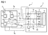
図1は、ビーム検出器1の実施例の概略図を示している。 FIG. 1 shows a schematic diagram of an embodiment of a beam detector 1.
ビーム検出器1は検出装置2と調整装置3を含んでいる。調整装置3は検出装置2と導電性に接続されており、検出装置内で形成された電気信号は調整装置に供給される。
The beam detector 1 includes a
検出装置2は多数の検出器部材4、5および6を含んでいる。これらの検出器部材は有利には、ビーム受信のため、およびビーム形成のために構成されている。有利には、多数の検出器部材は可視ビームを検出するために構成されている。例えば、3つの検出器部材が設けられており、これらは可視ビームの検出のために構成されている。有利には、これらの検出器部材には異なる検出領域、例えば種々異なる色のスペクトル領域が割り当てられている。従って検出器部材4を青色スペクトル領域における検出のために、検出器部材5を緑色スペクトル領域における検出のために、検出器部材6を赤色スペクトル領域における検出のために構成することができる。
The
多数の検出器部材、有利には、可視ビームの検出のために構成されている全ての検出器部材は化合物半導体材料を含んでいる。材料系InyAlxGa1−x−yP(ここで0≦x≦1および0≦xy≦1、有利にはx≠0、y≠0、x≠1および/またはy≠1)からのIII−V−族半導体材料は、Siに比べてその高い調達可能な量子効果および赤外スペクトル領域におけるその鈍感性のために、可視スペクトル領域に対するビーム検出器を構成するのに特に適している。検出されるべきビームから赤外成分をフィルタリング除去するための外部フィルタを、このような検出装置の場合には省くことができる。なぜなら検出器部材自体が既に、赤外スペクトル領域における無視できるまたは弱い感度を備えて構成されているからである。 A number of detector members, preferably all detector members configured for the detection of visible beams, comprise a compound semiconductor material. From the material system In y Al x Ga 1-xy P (where 0 ≦ x ≦ 1 and 0 ≦ xy ≦ 1, preferably x ≠ 0, y ≠ 0, x ≠ 1 and / or y ≠ 1) The III-V- group semiconductor material is particularly suitable for constructing a beam detector for the visible spectral region because of its high procurable quantum effect compared to Si and its insensitivity in the infrared spectral region. . An external filter for filtering out infrared components from the beam to be detected can be omitted in the case of such a detection device. This is because the detector member itself is already configured with negligible or weak sensitivity in the infrared spectral region.
検出器部材4、5および6は、共通の担体7上に配置されており、有利にはこの担体上に固定されている。担体7は例えばハウジング、殊に部材ハウジング、有利には表面実装可能な部材に対するハウジングを用いて形成されている。検出器部材に対する電気端子は分かりやすくするために詳細には示されていない。
The
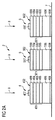
図2Aは検出装置2の実施例の概略的な断面図を示している。検出器部材4、5および6は別個に、かつ隣り合って、担体7上に配置された検出器部材として構成されている。例えば、検出器部材は不連続に配置された検出器チップとして構成されている。
FIG. 2A shows a schematic cross-sectional view of an embodiment of the
検出器部材4、5および6はそれぞれ1つの半導体ボディ401、501ないし601を有している。有利には半導体ボディはそれぞれ多数の半導体層を含んでいる。さらに検出器部材はそれぞれビーム入射面402、502ないし602を有している。これらのビーム入射面は、担体7と反対の方を向いている。
The
各検出器部材の半導体ボディ401、501ないし601は活性領域403、503ないし603を含んでいる。活性領域は、2つのバリヤ層404と405の間、504と505の間、ないしは604と605の間に配置されている。その間に活性領域が配置されているこれらのバリヤ層は有利には異なる導電型(p型ないしはn型)を有しており、このために有利には適切にドーピングされている。活性領域は半導体機能層を含んでおり、これは有利にはドーピングしないで構成されている。
The
検出器部材4、5および6の半導体ボディは、それぞれ基板406、506ないしは606上に配置されている。基板は、半導体ボディに対する半導体層の成長基板によって形成されてもよい。この成長基板の上に半導体層がエピタキシャルに成長される。
The semiconductor bodies of
さらに検出器部材4、5および6はそれぞれ2つの電気的コンタクト407および408、507および508ないしは607および608を有している。コンタクト408、508および608は例えば、基板の、各半導体ボディと反対の側を向いている側に配置され得る。コンタクト407、507および607は、属する半導体ボディの、各基板と反対の側を向いている側に配置され得る。これらの電気的コンタクトは、金属化部として構成され得る。
Further, the
電気的コンタクトは有利には、各活性領域と導電性に接続されている。従って、検出装置2に入射するビーム8からの成分を吸収することによって、活性領域において形成された電荷を、各検出器部材から導出することができ、このようにして検出器部材内で形成された信号が検出される。個々の検出器部材の信号はさらに相互に依存しないで検出される。
The electrical contacts are advantageously connected electrically to each active region. Therefore, by absorbing the component from the beam 8 incident on the
各半導体ボディ401、501ないし601はさらに、有利には、コンタクト層409、509ないしは609を有している。ビーム入射面の電気的コンタクト407、507ないし607への半導体ボディの電気的結合は、これによって改善される。コンタクト層は有利には例えばp型にドーピングされて構成される。
Each
各半導体ボディの半導体層は、有利には化合物半導体材料をベースにしている。可視スペクトル領域に対してはIII−V−族半導体材料が特に適している。活性領域は有利には材料系InyAlxGa1−x−yPをベースにしている。Al含量を介して、各活性領域を含むないしは活性領域を構成する、機能層の禁制帯が調整される。 The semiconductor layer of each semiconductor body is preferably based on a compound semiconductor material. III-V-group semiconductor materials are particularly suitable for the visible spectral region. The active region is preferably based on the material system In y Al x Ga 1-xy P. Through the Al content, the forbidden band of the functional layer including or constituting each active region is adjusted.
(成長)基板としては、材料系InyAlxGa1−x−yPの場合には、GaAs基板が特に適している。GaAs基板の良好な格子整合に関しては、基本材料系In0、b(Ga1−xAlx)0、bPを使用することが有利であることが判明している。各コンタクト層に対してはGaPが特に適している。 As the (growth) substrate, a GaAs substrate is particularly suitable in the case of the material system In y Al x Ga 1-xy P. For good lattice matching of GaAs substrates, it has been found advantageous to use the basic material system In 0, b (Ga 1-x Al x ) 0, b P. GaP is particularly suitable for each contact layer.
Al含量が増えるとともに、活性領域に対する半導体層の禁制帯が増大する。活性領域に対するAl含量の選択を介して、殊に、各検出器部材のスペクトル感度分布の長波境界波長が調整される。より長い波長のビーム、すなわちその波長が長波の境界波長よりも長いビームは、各検出器部材においてもはや重大な信号を生成しない。検出器部材4、5および6の長波の境界波長は有利にはそれぞれ可視スペクトル領域内にある。このような場合に外部フィルタ、例えば赤外ビームをフィルタリングするための外部フィルタを省くことができる。
As the Al content increases, the forbidden band of the semiconductor layer with respect to the active region increases. Through selection of the Al content for the active region, in particular, the long wave boundary wavelength of the spectral sensitivity distribution of each detector member is adjusted. A longer wavelength beam, ie a beam whose wavelength is longer than the long boundary wavelength, no longer produces a significant signal at each detector member. The longwave boundary wavelengths of the
図2Bにおける表は、図2Aに示された検出器部材の半導体層に対する材料の実施例を示している。さらに層厚、各禁制帯(EG)、この禁制帯に相応する波長(λG)、各層の導電型が示されている。検出器部材4は青色ビームを検出するために、検出器部材5は緑色のビームを検出するために、検出器部材6は赤色のビームを検出するために構成されている。
The table in FIG. 2B shows examples of materials for the semiconductor layers of the detector member shown in FIG. 2A. Furthermore, the layer thickness, each forbidden band (E G ), the wavelength (λ G ) corresponding to this forbidden band, and the conductivity type of each layer are shown. Detector member 4 is configured to detect a blue beam,
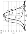
図2Cは検出器部材4、5および6のスペクトル感度分布のシミュレーションを示しており、ここでは半導体層が、図2Bの表に従って構成されると仮定されている。応答性Rの、入射ビームの波長λ(単位ナノメートル)への依存性が示されている。ここで応答性は、入射ビーム出力の各検出器部材内で形成されたフォト電流(ワット毎のアンペア:A/W)の強さを示している。
FIG. 2C shows a simulation of the spectral sensitivity distribution of
曲線600は検出器部材6の感度分布をあらわしており、曲線500は検出器部材5の感度分布をあらわしており、曲線400は検出器部材4の感度分布をあらわしている。Al含量が僅かであるので、検出器部材6は既に赤色スペクトル領域において感度が高い。検出器部材5はより多くのAl含量に基づいて、オレンジから緑色のスペクトル領域において高い感度値を有しており、検出器部材4は、さらに上昇しているAl含量によって主に青色スペクトル領域において高い感度を有している。
A
可視のスペクトル領域は、CIE(国際照明委員会)による明順応している人間の眼の感度分布700によって明確にされている。可視のスペクトル領域において全ての3つの検出器部材はある程度の感度を示す。例えば青色スペクトル領域においては3つの検出器部材において重大な信号が形成されるので、検出器部材の3つの信号から直接的に、入射ビームからの色成分を得るのは困難である。感度分布は殊に明確に分けられた感度チャネルを構成するのではなく、ある程度相互に覆っている。従って例えば分布600は、2つの他の分布を完全に覆っている。
The visible spectral region is defined by the
図3Aは検出装置2の別の実施例を概略的な断面図に基づいて示している。
FIG. 3A shows another embodiment of the
図2Aに示された検出装置とは異なり、検出器部材4、5および6は共通の半導体ボディ200内にモノリシックに集積されている。従って半導体ボディ200は、検出器部材4、5および6を含んでいる。半導体ボディ200は基板206上に配置されており、この上にエピタキシャル成長されていてよい。半導体ボディはさらにビーム入射面202を有している。検出器部材4、5および6は有利には次のように配置されている。すなわち、各活性領域403、503、603の機能層の禁制帯が、ビーム入力面202との間隔が増えるにつれて低減するように配置されている。不連続に隣り合って配置された検出器部材を備えている図2Aに示された検出装置とは異なり、相互に重なり合ってエピタキシャルに成長された多数の検出器部材を備えた、このようにモノリシックに集積された検出装置2は、それほど場所を必要としない。しかし検出装置2のこのような構成に対する製造コストは高い。
Unlike the detection device shown in FIG. 2A, the
検出器部材4、5および6内で形成された信号は、検出器部材に割り当てられた電気的コンタクトを介して相互に依存しないで検出される。ここで検出器部材4にはコンタクト210および211が、検出器部材5にはコンタクト211および212が、検出器部材6にはコンタクト212および213が割り当てられている。各検出器部材に割り当てられたコンタクトは、これらの検出器部材の活性領域と導電性に接続されている。隣接する2つの検出器部材はそれぞれ1つの共通のコンタクトを有している。これらのコンタクトは金属化部として構成され得る。
The signals formed in the
半導体ボディ200はさらにフィルタリング層214を有している。このフィルタリング層はモノリシックに半導体ボディ内に集積され、殊にエピタキシャルに成長可能である。このフィルタリング層204は有利には半導体ボディ内にビーム入力側に配置されており、特に有利には、活性領域の禁制帯よりも短い波長、殊にビーム出力側に配置された活性領域403の禁制帯に相応する波長に相応する波長を含んでいる波長領域においてビームを吸収している。フィルタリングされた波長領域において、活性領域において、これに相応する、低減された信号が生成される。フィルタリング層214は、検出装置の信号形成領域に対する窓層として使用される。
The
図3Bは、図3Aに相応して示された層に対するデータを含んでいる表を示している。これは検出器装置2のスペクトル感度部分に対するシミュレーションに基づいている(図3C参照)。 FIG. 3B shows a table containing data for the layers shown corresponding to FIG. 3A. This is based on a simulation of the spectral sensitivity part of the detector device 2 (see FIG. 3C).
検出器部材4、5ないし6の感度分布400、400および600は図3Cに示されている。図2Cに示された感度分布とは異なり、既に検出器部材の感度分布によって、明確な、スペクトル的に相互に分けられている感度チャネルが構成されている。感度分布は殊に、部分的にしか相互に重畳していない。従って入射ビームにおける色成分に関する情報を、直接的に検出器部材内で形成された信号から得るのは、図2に示された検出装置と比べて容易になる。
The
ビーム入射側の検出器部材4内で既に大部分の短い波長のビームが吸収されているので、このビームは後方に配置された検出器部材5および6内で、僅かにしか信号形成に関与しない。従って、検出器部材5および6は短い波長の領域において、多数の不連続に隣り合って配置された検出器部材を備えている、図2Aに示された検出装置の場合よりも僅かしか信号を生成しない。しかし場合によっては、図2に示された分散した検出器部材の場合でも、有利には(In、Ga、Al)Pベースまたは(Al)GaAsベースの適切なフィルタリング層を設けることを介して、顕著な感度チャネルに対する各感度分布の短い波長のエッジが、短い波長のビームを相応にフィルタリングすることによって抑圧される。相応するフィルタリング層は有利には、検出器部材5および6内に、中間の波長ビームおよび長い波長のビームに対して、各半導体ボディのビーム入射面と活性領域の間に配置される。
Since most of the short-wavelength beam has already been absorbed in the detector member 4 on the beam entrance side, this beam is only slightly involved in signal formation in the
従って図2Aに相応してこのようなフィルタリング層が設けられていない場合には、図2Cに示された感度分布において別個にされた感度チャネルを得る場合には、例えば、2つの感度分布からの差が形成される。 Thus, if such a filtering layer is not provided in accordance with FIG. 2A, to obtain separate sensitivity channels in the sensitivity distribution shown in FIG. 2C, for example, from two sensitivity distributions. A difference is formed.
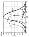
図2Dはこのような差形成から得られた、スペクトル原色である赤、緑および青の色検出のための感度チャネルを示している。さらに、明順応している人間の眼の感度分布700も示されており、これによって可視スペクトル領域が明確にされている。
FIG. 2D shows the sensitivity channels for color detection of the spectral primaries red, green and blue resulting from such difference formation. Also shown is a
長い波長の感度チャネル620は、図2Cに示された長い波長の感度分布600と中間の波長の感度分布500との差から形成される。中間の波長の感度チャネル520は中間の波長の感度分布500と短い波長の感度分布400との差から形成される。短い波長の感度チャネル420は、修正されていない検出器部材4のスペクトル感度分布によって形成される。
The long
検出器部材4,5ないし6の作動時には(例えば図2または3に応じた実施例に従って)、検出器部材内で形成された信号は、調整装置3に供給される(図1参照)。感度チャネルは既に、検出器部材のスペクトル感度分布の相応する形成によって設定されている(例えば図3C参照)。択一的に調整装置に、まだ、あらかじめ作られた感度チャネルには割り当てられてない信号が供給されてもよい(図2Cに示された幅の広い分布500および600を参照)。
During operation of the
調整装置は多数の入力側を有している(入力側E4、E5ないしE6参照)。有利には、検出器部材内で形成された信号S4、S5ないしS6はそれぞれ調整装置の個別の入力側に供給される。信号が調整装置に供給される前に、信号がさらに増幅されてもよい。この場合には担体7は有利にはプレ増幅器、特に有利には増幅器チップとして、例えばシリコンベースで構成されている。この場合には検出器部材4、5および6にはこの場合には、有利にはそれぞれ1つの増幅器入力側VE4、VE5ないしはVE6が割り当てられている(図1において破線で示された担体7の部材を参照)。
The adjusting device has a number of input sides (see input sides E 4 , E 5 to E 6 ). Advantageously, the signals S 4 , S 5 to S 6 formed in the detector member are each supplied to a separate input of the adjusting device. The signal may be further amplified before it is fed to the conditioning device. In this case, the
例えば図2に関連して示されたような分散された検出器部材の場合には、個々の検出器部材は有利にはそれぞれ、増幅器チップの個別の入力側上に配置されており、これらの入力側と導電性に接続されている。このような接続に対しては導電性接続層、例えば(銀)導電性接着剤層が特に適している。 In the case of a distributed detector member, for example as shown in connection with FIG. 2, the individual detector members are each preferably arranged on a separate input side of the amplifier chip, It is electrically connected to the input side. For such connections, a conductive connection layer, for example a (silver) conductive adhesive layer, is particularly suitable.
検出器部材内では強度が弱い強さ(例えばnAまたはμAのオーダーにある)の通常の信号が形成されるので、例えば厚さ1μm以下、有利には500μm以下の接続層を介した増幅器への短い接続経路が特に適している。妨害されやすい「弱い」信号が外部の電磁ノイズにさらされる経路は、導電性の層結合によって有利には僅かに保たれる。 A normal signal of weak strength (eg in the order of nA or μA) is formed in the detector member, so that it is connected to the amplifier via a connection layer, for example of thickness 1 μm or less, preferably 500 μm or less. A short connection path is particularly suitable. The path through which “weak” signals that are susceptible to interference are exposed to external electromagnetic noise is advantageously kept slightly by the conductive layer coupling.
増幅器チップの各検出器部材に割り当てられた出力側を介して、事前に増大された信号は調整装置3の各入力側に供給される(出力側VA4、VA5およびVA6並びに事前に増幅された信号SV4、SV5およびSV6を参照)。 Via the output assigned to each detector member of the amplifier chip, the pre-amplified signal is supplied to each input of the regulator 3 (outputs VA 4 , VA 5 and VA 6 and pre-amplification). Referring to signal SV 4, SV 5 and SV 6 that is).
検出器装置の信号が事前に増幅される形態は、調整装置までの破線で示された線によって示されている。ここで各検出器部材には有利にはちょうど1つの増幅入力側(VEi、i=4、5、6)および/または増幅出力側(VAi、i=4、5、6)が割り当てられている。 The form in which the signal of the detector device is pre-amplified is indicated by the dashed line to the adjustment device. Here, each detector member is preferably assigned exactly one amplification input (VE i , i = 4, 5, 6) and / or amplification output (VA i , i = 4, 5, 6). ing.
調整装置3は調整ユニット9を有している。調整ユニット9は有利には増幅器として構成されており、ここでは種々の感度チャネルからのチャネル信号K4、K5およびK6がそれぞれ種々異なる増幅器ファクタによって増幅される。調整ユニット9は、調整端子94、95および96を有しており、これらを介して、感度チャネルからのチャネル信号に対する増幅ファクタが、相互に依存しないで調整される。
The adjusting device 3 has an
検出器装置がまだ、事前に形成された感度チャネルを有していない場合(図2C参照)、調整ユニットは次のように構成される。すなわち、検出器部材内で形成された信号が、調整装置3内で、感度チャネルに割り当てられたチャネル信号が形成されるように処理されるように構成される。感度チャネルは調整装置内で有利には、信号が調整ユニットに供給される前にこのような装置の部材によって形成される。 If the detector device does not yet have a pre-formed sensitivity channel (see FIG. 2C), the adjustment unit is configured as follows. That is, the signal formed in the detector member is configured to be processed in the adjustment device 3 so as to form a channel signal assigned to the sensitivity channel. The sensitivity channel is advantageously formed in the adjusting device by means of such a device before the signal is supplied to the adjusting unit.
例えば差形成ユニット10が調整装置内に設けられ、これは検出装置から得られた信号から差を形成する。これによってチャネル信号が形成される(図2Dを参照)。
For example, a
調整ユニット9内では、チャネル信号の相対的な重み付けが相互に異なって調整される。
Within the
異なって重み付けされた複数のチャネル信号は次に、調整装置3の重畳ユニット11内で重畳される。有利には重畳ユニット11は異なって重み付けされたチャネル信号を、調整ユニット9を通過した後に重ねる。これは、重畳ユニット内の破線のラインによって示されている。
The differently weighted channel signals are then superimposed in the
異なって重み付けされたチャネル信号は重畳ユニット11内で、重畳され、殊に加算されてビーム検出器の検出器信号DSにされる。この検出器信号DSは、調整装置3の出力側Aで検出される。この出力側は重畳ユニット11と導電性に接続されている。
The differently weighted channel signals are superposed in the
調整装置3は、有利にはSiベースの、有利には集積回路として構成される。これによって、ビーム検出器1の小さく、かつコンパクトな構造が容易になる。 The adjusting device 3 is preferably configured as a Si-based, preferably as an integrated circuit. This facilitates a small and compact structure of the beam detector 1.
異なって重み付けされたチャネル信号の重畳によって、異なった感度分布(出力側Aでの出力信号DSの、波長への依存性)を有するビーム検出器が実現される。 By superimposing differently weighted channel signals, beam detectors having different sensitivity distributions (dependence of the output signal DS on the output side A on the wavelength) are realized.
例えば、ビーム検出器を、調整ユニット9を用いたチャネル信号の種々異なる重み付けによって、人間の眼の感度分布に応じた感度分布を有している周辺光センサとして構成することができる。これは、図4Aおよび4Bにおいて、図2Dに従った感度チャネルに対して示されている。
For example, the beam detector can be configured as an ambient light sensor having a sensitivity distribution corresponding to the sensitivity distribution of the human eye by different weighting of the channel signal using the
図4Aでは、明順応している人間の眼の感度分布に相応した感度分布に対する感度チャネルが重ねられている。個々の感度チャネルからの信号はこれ対して相互に相対して弱められているないしは増幅されている。図示された、重畳された感度分布701はファクタ0.9ぶんだけの感度チャネル620の増幅、ファクタ1.2ぶんだけの感度チャネル520の増幅、およびファクタ0.25ぶんだけの感度チャネル420の増幅によって得られる。加算された感度分布701は実質的に、明順応している人間の眼700に相応している。
In FIG. 4A, sensitivity channels for sensitivity distributions corresponding to the sensitivity distribution of the light-adapted human eye are overlaid. The signals from the individual sensitivity channels are weakened or amplified relative to each other. The superimposed
図4Bでは、赤色スペクトル領域に割り当てられている長い波長の感度チャネル620が抑圧されている。これは0の増幅ファクタに相応する。緑色のスペクトル領域に割り当てられている感度チャネル520は0.7のファクタによって増幅されており、青色のスペクトル領域に割り当てられている感度チャネル420は1.3のファクタによって増幅されている。加算された分布703は、近似的に暗順応している人間の眼702に相応する。暗順応している人間の眼の分布に対しては例えば、1951年のCIEに従った相応の分布が引き合いに出される。
In FIG. 4B, the long
検出器感度のスペクトル分布は有利には調整端子94、95および96を介して、明順応している人間の眼(分布700、図4A)のスペクトル感度と、暗順応している人間の眼(分布702、図4B)のスペクトル感度との間で切替可能である。切り替え過程は例えば、有利にはビーム検出器が含んでいる明るさ/暗さセンサ(詳細には図示されていない)によって制御される。モノリシック検出装置の感度チャネル(図3参照)も相応に種々異なって重み付けされ、各所望の分布に対して重畳される。
The spectral distribution of the detector sensitivity is advantageously adjusted via the
ビーム検出器1を周辺光センサとして作動させる他に、ビーム検出器を色センサとして、感度チャネルに相応する原色(この実施例において、赤色、緑色および青色)を検出するために使用することもできる。検出器信号を介して、この場合には、ビーム検出器に入射するビームにおける色成分が定められる。このような色成分から例えば、入射ビームの色位置または色印象が求められる。従って検出されるべき色に割り当てられていない感度チャネルからの信号関与は調整端子の相応する調整によって抑圧されている。 Besides operating the beam detector 1 as an ambient light sensor, the beam detector can also be used as a color sensor to detect the primary colors corresponding to the sensitivity channel (in this example, red, green and blue). . Via the detector signal, in this case the color component in the beam incident on the beam detector is determined. For example, the color position or color impression of the incident beam is obtained from such color components. Thus, signal involvement from sensitivity channels not assigned to the color to be detected is suppressed by a corresponding adjustment of the adjustment terminal.
さらに、ビーム検出器の所定の感度分布は相応の調整を介して調整端子で調整される。ビーム検出器は全体的に省スペースに構成され、有利には様々に使用可能である。 Furthermore, the predetermined sensitivity distribution of the beam detector is adjusted at the adjustment terminal via a corresponding adjustment. The beam detector is entirely space-saving and can be used in various ways.
図5Aは、多数の別個のスペクトル感度チャネル801・・・809を備えた検出装置のスペクトル感度分布を示す。感度チャネルはここで、相応する検出器部材のスペクトル感度分布によって構成される。このためには検出器部材は相応のフィルタリング層を有しており、これは各半導体ボディのビーム入力面と活性領域との間に配置されている。例えば9個の検出器部材が図2Aと同様に隣り合って配置されていてもよい。ここで図2Aに示された層構造に対して付加的に、ビーム入射面と各活性領域との間にフィルタリング層が設けられている。
FIG. 5A shows the spectral sensitivity distribution of a detector with a number of separate
検出器部材の感度分布に対してここでは、図5Bにおける表に相応するデータが使用される。 Here, data corresponding to the table in FIG. 5B is used for the sensitivity distribution of the detector elements.
活性領域はそれぞれ材料系InyAlxGa1−x−yPをベースにする。各フィルタリング層は、同一の材料系をベースにするかまたはGaPから成る。 The active regions are each based on the material system In y Al x Ga 1-xy P. Each filtering layer is based on the same material system or consists of GaP.
検出器部材のスペクトル感度分布は、それぞれ、可視スペクトル領域における波長λmaxで最大値を有している。 The spectral sensitivity distribution of a detector member, respectively, has a maximum value at a wavelength lambda max in the visible spectral region.
さらに個々の感度チャネルは狭帯域に構成されており、殊に少なくとも部分的に60nm以下、有利には40nm以下、特に有利には30nm以下、またはむしろ20nm以下のスペクトル幅を有している。 Furthermore, the individual sensitivity channels are arranged in a narrow band, in particular having a spectral width of at least partly 60 nm or less, preferably 40 nm or less, particularly preferably 30 nm or less, or rather 20 nm or less.
この多数の感度チャネルによって、可視スペクトル領域にわたってチャネルを細かく分割することで、一方では設定された感度分布を正確に模倣することが容易になり、他方では、キャッシュカードまたは紙幣の真偽性検査のための、特別なスペクトル線の検出も容易になる。 This multiple sensitivity channel makes it easy to accurately mimic the set sensitivity distribution on the one hand, by finely dividing the channel over the visible spectral region, and on the other hand for authenticity checking of cash cards or banknotes. Therefore, it becomes easy to detect special spectral lines.
特別なスペクトル線の検出の場合は、このようなスペクトル線の検出には必要とされない感度チャネルは有利には抑圧される。 In the case of special spectral line detection, sensitivity channels that are not required for such spectral line detection are advantageously suppressed.
さらに、図5Aは、暗順応している人間の眼のスペクトル感度分布702が示されている。図5Bの表からの個々の感度チャネルに対する増幅ファクタによって加算された感度分布703は、非常に正確に、暗順応している人間の眼702の感度分布に相応して延在する。
In addition, FIG. 5A shows a
図示されたチャネル801・・・809は色検出にも適している。ここで色情報は有利には、多数のチャネル信号から得られる。
The illustrated
有利には、ビーム検出器の作動状態(色センサとして、明順応している眼の周辺光センサとして、暗順応している眼の周辺光センサとして、または場合によってはスペクトル線センサとして)の調整は、例えばプログラミング可能なマイクロコントローラを介してプログラミングされる。マイクロコントローラは有利には、調整装置9の調整端子94、95、96と導電性に接続されている。
Advantageously, adjustment of the operating state of the beam detector (as a color sensor, as a light-adapted eye ambient light sensor, as a dark-adapted eye ambient light sensor, or in some cases as a spectral line sensor) Is programmed via, for example, a programmable microcontroller. The microcontroller is advantageously electrically connected to the
図6は、図1に示されたビーム検出器1の部分図を示している。ここでは図1に示されたビーム検出器に対して付加的に、このようなマイクロコントローラ12が調整装置9の調整端子94、95、96と導電性に接続されている。図1に示されたビーム検出器の別の部材は、図6においては分かりやすくするために詳細には示されていないが、当然ながら、設けられ得る。複数の調整端子はマイクロコントローラによって有利には相互に依存しないで制御可能である。例えば調整端子94、95および96はそれぞれ、マイクロコントローラの特別な電気的コンタクト124、125ないし126と導電性に接続されている。
FIG. 6 shows a partial view of the beam detector 1 shown in FIG. Here, in addition to the beam detector shown in FIG. 1, such a
マイクロコントローラ12は有利には次のようにプログラミングされている。すなわちマイクロコントローラが、調整端子をビーム検出器の設定されている作動状態(例えば色センサとして、明順応している眼の周辺光センサとして、暗順応している眼の周辺光センサとして、またはスペクトル線センサとして)に従って駆動制御するようにプログラミングされている。ユーザはこの場合には、マイクロコントローラの相応する応答を介して所定の作動状態を自由に切替する。従って、各作動状態に対して適している調整端子の相互の調整をユーザ側で手間がかかって求めることはしなくてよい。このような調整はむしろ既に工場側で、マイクロコントローラの相応するプログラミングによって実施される。
The
択一的または付加的にマイクロコントローラは作動状態を時間で制御し、例えば時刻に関して制御することができる。例えばマイクロコントローラは次のようにプログラミングされる。すなわちマイクロコントローラが特定の時刻から、有利には日暮れになった後に、周辺光センサとしてのビーム検出器の作動時に、暗順応している人間の眼に従った検出だけを許可するようにプログラミングされる。有利には、マイクロコントローラはユーザによってプログラミング可能であり、従ってビーム検出器の作動状態間の切替、殊に時間制御された切替を、ユーザ側で事前に調整することができる。 Alternatively or additionally, the microcontroller can control the operating state with time, for example with respect to time. For example, the microcontroller is programmed as follows. That is, the microcontroller is programmed to only allow detection according to the dark-adapting human eye when the beam detector as an ambient light sensor is activated from a specific time, preferably after sunset. The Advantageously, the microcontroller is programmable by the user, so that switching between the operating states of the beam detector, in particular time-controlled switching, can be adjusted in advance on the user side.
この特許出願は、2006年11月30日付けのドイツ特許出願第102006056579.7号の優先権および2007年3月13日付けの第102007012115.8号の優先権を主張しており、これらの文献の全体的な開示内容は本願に明確に参照として取り入れられている。 This patent application claims the priority of German patent application 102006056579.7 dated November 30, 2006 and the priority number 1000701211155.8 dated March 13, 2007. The entire disclosure of is hereby expressly incorporated by reference.
本願は、実施例に基づく記載によって制限されない。むしろ本発明はそれぞれ新たな特徴並びに特徴の各組み合わせを含んでおり、これは殊に特許請求の範囲に記載された特徴の各組み合わせを含んでいるが、これらの特徴またはこれらの組み合わせ自体が明確には、特許請求の範囲または実施例に記載されていない場合にも当てはまる。 This application is not restrict | limited by the description based on an Example. Rather, each invention includes each new feature and each combination of features, which in particular includes each combination of features recited in the claims, but these features or combinations of these are themselves unambiguous. Is also true when not stated in the claims or examples.
Claims (23)
当該検出装置は多数の検出器部材(4、5、6)を有しており、
前記ビーム検出器の作動時に当該検出器部材によって検出器信号(DS)が得られ、
・前記検出器部材はそれぞれ1つのスペクトル感度分布(400、500、600)を有しており、信号形成(S4、S5、S6)に適しており、
・少なくとも1つの検出器部材は化合物半導体材料を含んでおり、かつ当該検出器部材は可視スペクトル領域におけるビームを検出するために構成されており、
・前記検出器部材の感度分布によって、ビーム検出器の種々異なるスペクトル感度チャネル(420、520、620)が形成されるように、前記ビーム検出器が構成されており、
・前記感度チャネルにおいて、前記検出器部材によって、各感度チャネルに割り当てられたチャネル信号(K4、K5、K6)が形成され、
・種々異なるチャネル信号の、ビーム検出器の検出信号に対する関与が異なって調整されるように、前記調整装置が構成されている、
ことを特徴とするビーム検出器。 A beam detector (1) comprising a detection device (2) and an adjustment device (3),
The detection device has a number of detector members (4, 5, 6),
When the beam detector is activated, a detector signal (DS) is obtained by the detector member;
The detector members each have one spectral sensitivity distribution (400, 500, 600) and are suitable for signal formation (S 4 , S 5 , S 6 );
At least one detector member comprises a compound semiconductor material, and the detector member is configured to detect a beam in the visible spectral region;
The beam detector is configured such that the sensitivity distribution of the detector member forms different spectral sensitivity channels (420, 520, 620) of the beam detector;
In the sensitivity channel, the detector members form channel signals (K 4 , K 5 , K 6 ) assigned to each sensitivity channel;
The adjusting device is configured such that the involvement of different channel signals with respect to the detection signal of the beam detector is adjusted differently;
A beam detector characterized by that.
Applications Claiming Priority (3)
| Application Number | Priority Date | Filing Date | Title |
|---|---|---|---|
| DE102006056579 | 2006-11-30 | ||
| DE102007012115A DE102007012115A1 (en) | 2006-11-30 | 2007-03-13 | radiation detector |
| PCT/EP2007/063007 WO2008065170A1 (en) | 2006-11-30 | 2007-11-29 | Radiation detector with an adjustable spectral sensitivity |
Publications (2)
| Publication Number | Publication Date |
|---|---|
| JP2010511162A true JP2010511162A (en) | 2010-04-08 |
| JP2010511162A5 JP2010511162A5 (en) | 2011-10-13 |
Family
ID=39110400
Family Applications (1)
| Application Number | Title | Priority Date | Filing Date |
|---|---|---|---|
| JP2009538716A Pending JP2010511162A (en) | 2006-11-30 | 2007-11-29 | Beam detector with adjustable spectral sensitivity |
Country Status (8)
| Country | Link |
|---|---|
| US (1) | US8274657B2 (en) |
| EP (1) | EP2054705A1 (en) |
| JP (1) | JP2010511162A (en) |
| KR (1) | KR101430030B1 (en) |
| CN (1) | CN101535785B (en) |
| DE (1) | DE102007012115A1 (en) |
| TW (1) | TWI365976B (en) |
| WO (1) | WO2008065170A1 (en) |
Cited By (1)
| Publication number | Priority date | Publication date | Assignee | Title |
|---|---|---|---|---|
| WO2022003813A1 (en) * | 2020-06-30 | 2022-01-06 | シャープ株式会社 | Electromagnetic wave sensor device and display device |
Families Citing this family (24)
| Publication number | Priority date | Publication date | Assignee | Title |
|---|---|---|---|---|
| US7442629B2 (en) | 2004-09-24 | 2008-10-28 | President & Fellows Of Harvard College | Femtosecond laser-induced formation of submicrometer spikes on a semiconductor substrate |
| US7057256B2 (en) | 2001-05-25 | 2006-06-06 | President & Fellows Of Harvard College | Silicon-based visible and near-infrared optoelectric devices |
| US7890055B1 (en) * | 2007-07-09 | 2011-02-15 | Everlokt Corporation | Touch field compound field detector personal ID |
| JP2010112807A (en) * | 2008-11-05 | 2010-05-20 | Hioki Ee Corp | Optical power meter |
| JP2010112808A (en) * | 2008-11-05 | 2010-05-20 | Hioki Ee Corp | Optical power meter |
| US8008613B2 (en) | 2009-05-05 | 2011-08-30 | Apple Inc. | Light sensing device having a color sensor and a clear sensor for infrared rejection |
| DE102009024069A1 (en) * | 2009-06-05 | 2010-12-09 | Osram Opto Semiconductors Gmbh | Optical lighting device and optical recording device |
| US9673243B2 (en) | 2009-09-17 | 2017-06-06 | Sionyx, Llc | Photosensitive imaging devices and associated methods |
| US9911781B2 (en) | 2009-09-17 | 2018-03-06 | Sionyx, Llc | Photosensitive imaging devices and associated methods |
| KR101893331B1 (en) * | 2009-09-17 | 2018-08-30 | 사이오닉스, 엘엘씨 | Photosensitive imaging devices and associated methods |
| KR101354791B1 (en) * | 2009-10-05 | 2014-01-22 | 가부시키가이샤 시마쓰세사쿠쇼 | Radiation detector |
| US8692198B2 (en) | 2010-04-21 | 2014-04-08 | Sionyx, Inc. | Photosensitive imaging devices and associated methods |
| US20120146172A1 (en) | 2010-06-18 | 2012-06-14 | Sionyx, Inc. | High Speed Photosensitive Devices and Associated Methods |
| KR102025522B1 (en) | 2011-03-10 | 2019-11-26 | 사이오닉스, 엘엘씨 | Three dimensional sensors, systems, and associated methods |
| JP2014509746A (en) | 2011-03-29 | 2014-04-21 | オスラム オプト セミコンダクターズ ゲゼルシャフト ミット ベシュレンクテル ハフツング | Unit for finding the dominant light source type using two photodiodes |
| US9496308B2 (en) | 2011-06-09 | 2016-11-15 | Sionyx, Llc | Process module for increasing the response of backside illuminated photosensitive imagers and associated methods |
| EP2732402A2 (en) | 2011-07-13 | 2014-05-21 | Sionyx, Inc. | Biometric imaging devices and associated methods |
| US8865507B2 (en) | 2011-09-16 | 2014-10-21 | Sionyx, Inc. | Integrated visible and infrared imager devices and associated methods |
| US9064764B2 (en) | 2012-03-22 | 2015-06-23 | Sionyx, Inc. | Pixel isolation elements, devices, and associated methods |
| WO2014127376A2 (en) | 2013-02-15 | 2014-08-21 | Sionyx, Inc. | High dynamic range cmos image sensor having anti-blooming properties and associated methods |
| US9939251B2 (en) | 2013-03-15 | 2018-04-10 | Sionyx, Llc | Three dimensional imaging utilizing stacked imager devices and associated methods |
| WO2014209421A1 (en) | 2013-06-29 | 2014-12-31 | Sionyx, Inc. | Shallow trench textured regions and associated methods |
| US10281329B2 (en) * | 2017-06-14 | 2019-05-07 | Simmonds Precision Products, Inc. | Method and system for fast determination of the wavelength of a light beam |
| CN109556710B (en) * | 2018-12-28 | 2024-04-16 | 浙江智慧照明技术有限公司 | Lighting ambient light sensor |
Citations (9)
| Publication number | Priority date | Publication date | Assignee | Title |
|---|---|---|---|---|
| DE2920773A1 (en) * | 1979-05-22 | 1980-12-04 | Siemens Ag | Opto-electronic sensor circuit - has two separately adjusted photodiodes controlling integrated evaluation loop |
| JPS6336121A (en) * | 1986-07-29 | 1988-02-16 | Minolta Camera Co Ltd | Colorimetric sensor |
| JPH01233328A (en) * | 1988-03-14 | 1989-09-19 | Agency Of Ind Science & Technol | Photometric apparatus |
| JPH03202732A (en) * | 1989-06-13 | 1991-09-04 | Sharp Corp | Color sensor |
| JP2000066166A (en) * | 1998-08-21 | 2000-03-03 | Mitsubishi Electric Corp | Projection type liquid crystal display device |
| DE10101457A1 (en) * | 2001-01-10 | 2002-07-18 | Infineon Technologies Ag | Detection of electromagnetic radiation using two or more optoelectronic semiconductor sensors combined such that the desired output response is obtained |
| EP1521069A2 (en) * | 2003-10-02 | 2005-04-06 | MAZet GmbH | Colorimeter for true colour measurement |
| JP2006108675A (en) * | 2004-09-30 | 2006-04-20 | Osram Opto Semiconductors Gmbh | Beam detector |
| JP2006189291A (en) * | 2005-01-05 | 2006-07-20 | Konica Minolta Sensing Inc | Photometric system and photometric method for monochromatic light |
Family Cites Families (25)
| Publication number | Priority date | Publication date | Assignee | Title |
|---|---|---|---|---|
| JPS55104725A (en) | 1979-02-05 | 1980-08-11 | Nec Corp | Wave-length discrimination type photo-detector |
| JPS59227171A (en) | 1983-06-08 | 1984-12-20 | Oki Electric Ind Co Ltd | Color sensor |
| US4758734A (en) | 1984-03-13 | 1988-07-19 | Nec Corporation | High resolution image sensor array using amorphous photo-diodes |
| JPH0612808B2 (en) | 1984-07-13 | 1994-02-16 | 日本電気株式会社 | Method of manufacturing solid-state imaging device |
| DE4024011A1 (en) * | 1990-07-28 | 1992-01-30 | Gossen Gmbh | Electronic light metering for automatic exposure cameras - using sensors with different spectral sensitivity and evaluating digitised signals according to film spectral sensitivities |
| JPH04280678A (en) * | 1991-03-08 | 1992-10-06 | Nec Corp | Solid-state image pickly element |
| DE4143284A1 (en) | 1991-12-30 | 1992-10-01 | Klaus Eberhard Engel | INTEGRATED SEMICONDUCTOR SENSOR FOR SPECTROMETER |
| GB2277405A (en) | 1993-04-22 | 1994-10-26 | Sharp Kk | Semiconductor colour display or detector array |
| US5362969A (en) | 1993-04-23 | 1994-11-08 | Luxtron Corporation | Processing endpoint detecting technique and detector structure using multiple radiation sources or discrete detectors |
| EP0645826A3 (en) | 1993-09-23 | 1995-05-17 | Siemens Comp Inc | Monolithic, multiple-channel optical coupler. |
| EP0852709A1 (en) * | 1995-09-27 | 1998-07-15 | Fraunhofer-Gesellschaft Zur Förderung Der Angewandten Forschung E.V. | Multispectral sensor device |
| CA2171574C (en) * | 1996-03-12 | 2000-10-03 | Brian W. Tansley | Photometric measurement apparatus |
| US6307660B1 (en) | 1997-01-28 | 2001-10-23 | Tellium, Inc. | Optical receiver particularly useful for a multi-wavelength receiver array |
| US6359274B1 (en) | 1999-01-25 | 2002-03-19 | Gentex Corporation | Photodiode light sensor |
| US6407439B1 (en) | 1999-08-19 | 2002-06-18 | Epitaxial Technologies, Llc | Programmable multi-wavelength detector array |
| US7065035B1 (en) | 1999-10-25 | 2006-06-20 | Matsushita Electric Industrial Co., Ltd. | Optical multilayer disk, multiwavelength light source, and optical system using them |
| US6380532B1 (en) | 2000-04-19 | 2002-04-30 | Eaton Corporation | Optical object detector with multiple photodetectors |
| GB2381950A (en) | 2001-11-06 | 2003-05-14 | Denselight Semiconductors Pte | Field effect based photodetector array responsivity control |
| TW499577B (en) | 2001-12-07 | 2002-08-21 | Univ Yuan Ze | Coiled optical fiber wavelength - power converter |
| DE102004037020B4 (en) * | 2003-09-30 | 2021-10-21 | OSRAM Opto Semiconductors Gesellschaft mit beschränkter Haftung | Radiation detector for the detection of radiation according to a predetermined spectral sensitivity distribution |
| DE10345410A1 (en) | 2003-09-30 | 2005-05-04 | Osram Opto Semiconductors Gmbh | radiation detector |
| US8212285B2 (en) | 2004-03-31 | 2012-07-03 | Osram Opto Semiconductors Gmbh | Radiation detector |
| DE102005001280B4 (en) * | 2004-09-30 | 2022-03-03 | OSRAM Opto Semiconductors Gesellschaft mit beschränkter Haftung | radiation detector |
| EP1667246A1 (en) * | 2004-12-03 | 2006-06-07 | ETeCH AG | A multi-colour sensitive device for colour image sensing |
| DE102005043918B4 (en) | 2005-05-30 | 2014-12-04 | Osram Opto Semiconductors Gmbh | Detector arrangement and method for determining spectral components in a radiation incident on a detector arrangement |
-
2007
- 2007-03-13 DE DE102007012115A patent/DE102007012115A1/en not_active Ceased
- 2007-11-26 TW TW096144735A patent/TWI365976B/en active
- 2007-11-29 WO PCT/EP2007/063007 patent/WO2008065170A1/en active Application Filing
- 2007-11-29 CN CN2007800414217A patent/CN101535785B/en active Active
- 2007-11-29 US US12/516,831 patent/US8274657B2/en active Active
- 2007-11-29 EP EP07847523A patent/EP2054705A1/en not_active Ceased
- 2007-11-29 KR KR1020097013679A patent/KR101430030B1/en active IP Right Grant
- 2007-11-29 JP JP2009538716A patent/JP2010511162A/en active Pending
Patent Citations (9)
| Publication number | Priority date | Publication date | Assignee | Title |
|---|---|---|---|---|
| DE2920773A1 (en) * | 1979-05-22 | 1980-12-04 | Siemens Ag | Opto-electronic sensor circuit - has two separately adjusted photodiodes controlling integrated evaluation loop |
| JPS6336121A (en) * | 1986-07-29 | 1988-02-16 | Minolta Camera Co Ltd | Colorimetric sensor |
| JPH01233328A (en) * | 1988-03-14 | 1989-09-19 | Agency Of Ind Science & Technol | Photometric apparatus |
| JPH03202732A (en) * | 1989-06-13 | 1991-09-04 | Sharp Corp | Color sensor |
| JP2000066166A (en) * | 1998-08-21 | 2000-03-03 | Mitsubishi Electric Corp | Projection type liquid crystal display device |
| DE10101457A1 (en) * | 2001-01-10 | 2002-07-18 | Infineon Technologies Ag | Detection of electromagnetic radiation using two or more optoelectronic semiconductor sensors combined such that the desired output response is obtained |
| EP1521069A2 (en) * | 2003-10-02 | 2005-04-06 | MAZet GmbH | Colorimeter for true colour measurement |
| JP2006108675A (en) * | 2004-09-30 | 2006-04-20 | Osram Opto Semiconductors Gmbh | Beam detector |
| JP2006189291A (en) * | 2005-01-05 | 2006-07-20 | Konica Minolta Sensing Inc | Photometric system and photometric method for monochromatic light |
Cited By (1)
| Publication number | Priority date | Publication date | Assignee | Title |
|---|---|---|---|---|
| WO2022003813A1 (en) * | 2020-06-30 | 2022-01-06 | シャープ株式会社 | Electromagnetic wave sensor device and display device |
Also Published As
| Publication number | Publication date |
|---|---|
| CN101535785B (en) | 2011-12-28 |
| WO2008065170A1 (en) | 2008-06-05 |
| US8274657B2 (en) | 2012-09-25 |
| TWI365976B (en) | 2012-06-11 |
| KR20090098850A (en) | 2009-09-17 |
| US20100097609A1 (en) | 2010-04-22 |
| TW200844412A (en) | 2008-11-16 |
| EP2054705A1 (en) | 2009-05-06 |
| DE102007012115A1 (en) | 2008-06-05 |
| KR101430030B1 (en) | 2014-08-14 |
| CN101535785A (en) | 2009-09-16 |
Similar Documents
| Publication | Publication Date | Title |
|---|---|---|
| JP2010511162A (en) | Beam detector with adjustable spectral sensitivity | |
| JP5166687B2 (en) | Beam detector | |
| US8803270B2 (en) | Light sensor having IR cut and color pass interference filter integrated on-chip | |
| CN106252368B (en) | Image sensor, method of manufacturing the same, and electro-optical system including the same | |
| US7248297B2 (en) | Integrated color pixel (ICP) | |
| US7858921B2 (en) | Guided-mode-resonance transmission color filters for color generation in CMOS image sensors | |
| US7329895B2 (en) | Dual wavelength detector | |
| TWI357494B (en) | Photodetector having dark current correction | |
| US8212285B2 (en) | Radiation detector | |
| CN1766533B (en) | Optical color sensor using diffractive elements | |
| JP2007531290A (en) | Radiation detector | |
| US20130309803A1 (en) | Radiation sensor with photodiodes being integrated on a semiconductor substrate and corresponding integration process | |
| WO2017058109A1 (en) | Optoelectronic modules for the acquisition of spectral and distance data | |
| US20020117658A1 (en) | Multi-quantum-well infrared sensor array in spatially-separated multi-band configuration | |
| CN207731929U (en) | Imaging sensor and imaging system | |
| US20030075767A1 (en) | High sensitivity polarized-light discriminator device | |
| KR20180071192A (en) | Image sensor and electronic device including the same | |
| CN101981696B (en) | Optoelectronic radiation detector and method for producing a plurality of detector elements | |
| TWI376784B (en) | Detector arrangement and detector component | |
| US20080105820A1 (en) | Resonant structures for electromagnetic energy detection system and associated methods | |
| JPH0555622A (en) | Semiconductor photodetector | |
| KR20100079452A (en) | Image sensor | |
| JPH01282875A (en) | Color sensor | |
| JPH03278476A (en) | Photosensor |
Legal Events
| Date | Code | Title | Description |
|---|---|---|---|
| A621 | Written request for application examination |
Free format text: JAPANESE INTERMEDIATE CODE: A621 Effective date: 20100809 |
|
| RD04 | Notification of resignation of power of attorney |
Free format text: JAPANESE INTERMEDIATE CODE: A7424 Effective date: 20101228 |
|
| A521 | Written amendment |
Free format text: JAPANESE INTERMEDIATE CODE: A523 Effective date: 20110823 |
|
| A977 | Report on retrieval |
Free format text: JAPANESE INTERMEDIATE CODE: A971007 Effective date: 20120524 |
|
| A131 | Notification of reasons for refusal |
Free format text: JAPANESE INTERMEDIATE CODE: A131 Effective date: 20120530 |
|
| A601 | Written request for extension of time |
Free format text: JAPANESE INTERMEDIATE CODE: A601 Effective date: 20120829 |
|
| A602 | Written permission of extension of time |
Free format text: JAPANESE INTERMEDIATE CODE: A602 Effective date: 20120905 |
|
| A521 | Written amendment |
Free format text: JAPANESE INTERMEDIATE CODE: A523 Effective date: 20121001 |
|
| A02 | Decision of refusal |
Free format text: JAPANESE INTERMEDIATE CODE: A02 Effective date: 20130201 |