JP2010511162A - 調整可能なスペクトル感度を備えたビーム検出器 - Google Patents
調整可能なスペクトル感度を備えたビーム検出器 Download PDFInfo
- Publication number
- JP2010511162A JP2010511162A JP2009538716A JP2009538716A JP2010511162A JP 2010511162 A JP2010511162 A JP 2010511162A JP 2009538716 A JP2009538716 A JP 2009538716A JP 2009538716 A JP2009538716 A JP 2009538716A JP 2010511162 A JP2010511162 A JP 2010511162A
- Authority
- JP
- Japan
- Prior art keywords
- detector
- sensitivity
- beam detector
- channel
- members
- Prior art date
- Legal status (The legal status is an assumption and is not a legal conclusion. Google has not performed a legal analysis and makes no representation as to the accuracy of the status listed.)
- Pending
Links
- 230000035945 sensitivity Effects 0.000 title claims abstract description 174
- 230000003595 spectral effect Effects 0.000 title claims abstract description 106
- 238000009826 distribution Methods 0.000 claims abstract description 97
- 239000004065 semiconductor Substances 0.000 claims abstract description 68
- 238000001514 detection method Methods 0.000 claims abstract description 65
- 239000000463 material Substances 0.000 claims abstract description 36
- 150000001875 compounds Chemical class 0.000 claims abstract description 20
- 230000015572 biosynthetic process Effects 0.000 claims abstract description 12
- 229910052782 aluminium Inorganic materials 0.000 claims description 4
- 239000003086 colorant Substances 0.000 claims description 4
- 229910052733 gallium Inorganic materials 0.000 claims description 4
- 229910052738 indium Inorganic materials 0.000 claims description 4
- 239000010410 layer Substances 0.000 description 44
- 238000001914 filtration Methods 0.000 description 21
- 230000003321 amplification Effects 0.000 description 12
- 238000003199 nucleic acid amplification method Methods 0.000 description 12
- 239000000758 substrate Substances 0.000 description 10
- XUIMIQQOPSSXEZ-UHFFFAOYSA-N Silicon Chemical compound [Si] XUIMIQQOPSSXEZ-UHFFFAOYSA-N 0.000 description 5
- 229910052710 silicon Inorganic materials 0.000 description 5
- 239000010703 silicon Substances 0.000 description 5
- 229910001218 Gallium arsenide Inorganic materials 0.000 description 3
- 239000008186 active pharmaceutical agent Substances 0.000 description 3
- 239000002346 layers by function Substances 0.000 description 3
- 238000004519 manufacturing process Methods 0.000 description 3
- 230000004044 response Effects 0.000 description 3
- 238000001228 spectrum Methods 0.000 description 3
- 230000004888 barrier function Effects 0.000 description 2
- 230000003750 conditioning effect Effects 0.000 description 2
- 230000008878 coupling Effects 0.000 description 2
- 238000010168 coupling process Methods 0.000 description 2
- 238000005859 coupling reaction Methods 0.000 description 2
- 230000001419 dependent effect Effects 0.000 description 2
- 238000010586 diagram Methods 0.000 description 2
- 230000000694 effects Effects 0.000 description 2
- 238000001465 metallisation Methods 0.000 description 2
- 238000000034 method Methods 0.000 description 2
- 230000008569 process Effects 0.000 description 2
- 238000004088 simulation Methods 0.000 description 2
- 230000009471 action Effects 0.000 description 1
- 239000012790 adhesive layer Substances 0.000 description 1
- 230000002238 attenuated effect Effects 0.000 description 1
- 238000011161 development Methods 0.000 description 1
- 230000018109 developmental process Effects 0.000 description 1
- 230000007274 generation of a signal involved in cell-cell signaling Effects 0.000 description 1
- 238000005286 illumination Methods 0.000 description 1
- 230000003278 mimic effect Effects 0.000 description 1
- 230000004043 responsiveness Effects 0.000 description 1
- 229910052709 silver Inorganic materials 0.000 description 1
- 239000004332 silver Substances 0.000 description 1
- 230000001629 suppression Effects 0.000 description 1
- 238000012795 verification Methods 0.000 description 1
- 230000003313 weakening effect Effects 0.000 description 1
Images


Classifications
-
- G—PHYSICS
- G01—MEASURING; TESTING
- G01J—MEASUREMENT OF INTENSITY, VELOCITY, SPECTRAL CONTENT, POLARISATION, PHASE OR PULSE CHARACTERISTICS OF INFRARED, VISIBLE OR ULTRAVIOLET LIGHT; COLORIMETRY; RADIATION PYROMETRY
- G01J1/00—Photometry, e.g. photographic exposure meter
- G01J1/42—Photometry, e.g. photographic exposure meter using electric radiation detectors
- G01J1/4228—Photometry, e.g. photographic exposure meter using electric radiation detectors arrangements with two or more detectors, e.g. for sensitivity compensation
-
- H—ELECTRICITY
- H10—SEMICONDUCTOR DEVICES; ELECTRIC SOLID-STATE DEVICES NOT OTHERWISE PROVIDED FOR
- H10F—INORGANIC SEMICONDUCTOR DEVICES SENSITIVE TO INFRARED RADIATION, LIGHT, ELECTROMAGNETIC RADIATION OF SHORTER WAVELENGTH OR CORPUSCULAR RADIATION
- H10F99/00—Subject matter not provided for in other groups of this subclass
-
- G—PHYSICS
- G01—MEASURING; TESTING
- G01J—MEASUREMENT OF INTENSITY, VELOCITY, SPECTRAL CONTENT, POLARISATION, PHASE OR PULSE CHARACTERISTICS OF INFRARED, VISIBLE OR ULTRAVIOLET LIGHT; COLORIMETRY; RADIATION PYROMETRY
- G01J1/00—Photometry, e.g. photographic exposure meter
- G01J1/42—Photometry, e.g. photographic exposure meter using electric radiation detectors
-
- G—PHYSICS
- G01—MEASURING; TESTING
- G01J—MEASUREMENT OF INTENSITY, VELOCITY, SPECTRAL CONTENT, POLARISATION, PHASE OR PULSE CHARACTERISTICS OF INFRARED, VISIBLE OR ULTRAVIOLET LIGHT; COLORIMETRY; RADIATION PYROMETRY
- G01J3/00—Spectrometry; Spectrophotometry; Monochromators; Measuring colours
- G01J3/28—Investigating the spectrum
- G01J3/30—Measuring the intensity of spectral lines directly on the spectrum itself
- G01J3/36—Investigating two or more bands of a spectrum by separate detectors
-
- G—PHYSICS
- G01—MEASURING; TESTING
- G01J—MEASUREMENT OF INTENSITY, VELOCITY, SPECTRAL CONTENT, POLARISATION, PHASE OR PULSE CHARACTERISTICS OF INFRARED, VISIBLE OR ULTRAVIOLET LIGHT; COLORIMETRY; RADIATION PYROMETRY
- G01J3/00—Spectrometry; Spectrophotometry; Monochromators; Measuring colours
- G01J3/46—Measurement of colour; Colour measuring devices, e.g. colorimeters
- G01J3/465—Measurement of colour; Colour measuring devices, e.g. colorimeters taking into account the colour perception of the eye; using tristimulus detection
-
- G—PHYSICS
- G01—MEASURING; TESTING
- G01J—MEASUREMENT OF INTENSITY, VELOCITY, SPECTRAL CONTENT, POLARISATION, PHASE OR PULSE CHARACTERISTICS OF INFRARED, VISIBLE OR ULTRAVIOLET LIGHT; COLORIMETRY; RADIATION PYROMETRY
- G01J3/00—Spectrometry; Spectrophotometry; Monochromators; Measuring colours
- G01J3/46—Measurement of colour; Colour measuring devices, e.g. colorimeters
- G01J3/50—Measurement of colour; Colour measuring devices, e.g. colorimeters using electric radiation detectors
- G01J3/51—Measurement of colour; Colour measuring devices, e.g. colorimeters using electric radiation detectors using colour filters
- G01J3/513—Measurement of colour; Colour measuring devices, e.g. colorimeters using electric radiation detectors using colour filters having fixed filter-detector pairs
-
- H—ELECTRICITY
- H10—SEMICONDUCTOR DEVICES; ELECTRIC SOLID-STATE DEVICES NOT OTHERWISE PROVIDED FOR
- H10F—INORGANIC SEMICONDUCTOR DEVICES SENSITIVE TO INFRARED RADIATION, LIGHT, ELECTROMAGNETIC RADIATION OF SHORTER WAVELENGTH OR CORPUSCULAR RADIATION
- H10F30/00—Individual radiation-sensitive semiconductor devices in which radiation controls the flow of current through the devices, e.g. photodetectors
- H10F30/20—Individual radiation-sensitive semiconductor devices in which radiation controls the flow of current through the devices, e.g. photodetectors the devices having potential barriers, e.g. phototransistors
- H10F30/21—Individual radiation-sensitive semiconductor devices in which radiation controls the flow of current through the devices, e.g. photodetectors the devices having potential barriers, e.g. phototransistors the devices being sensitive to infrared, visible or ultraviolet radiation
- H10F30/22—Individual radiation-sensitive semiconductor devices in which radiation controls the flow of current through the devices, e.g. photodetectors the devices having potential barriers, e.g. phototransistors the devices being sensitive to infrared, visible or ultraviolet radiation the devices having only one potential barrier, e.g. photodiodes
- H10F30/223—Individual radiation-sensitive semiconductor devices in which radiation controls the flow of current through the devices, e.g. photodetectors the devices having potential barriers, e.g. phototransistors the devices being sensitive to infrared, visible or ultraviolet radiation the devices having only one potential barrier, e.g. photodiodes the potential barrier being a PIN barrier
-
- G—PHYSICS
- G01—MEASURING; TESTING
- G01J—MEASUREMENT OF INTENSITY, VELOCITY, SPECTRAL CONTENT, POLARISATION, PHASE OR PULSE CHARACTERISTICS OF INFRARED, VISIBLE OR ULTRAVIOLET LIGHT; COLORIMETRY; RADIATION PYROMETRY
- G01J1/00—Photometry, e.g. photographic exposure meter
- G01J1/02—Details
- G01J1/04—Optical or mechanical part supplementary adjustable parts
- G01J1/0488—Optical or mechanical part supplementary adjustable parts with spectral filtering
-
- G—PHYSICS
- G01—MEASURING; TESTING
- G01J—MEASUREMENT OF INTENSITY, VELOCITY, SPECTRAL CONTENT, POLARISATION, PHASE OR PULSE CHARACTERISTICS OF INFRARED, VISIBLE OR ULTRAVIOLET LIGHT; COLORIMETRY; RADIATION PYROMETRY
- G01J3/00—Spectrometry; Spectrophotometry; Monochromators; Measuring colours
- G01J3/46—Measurement of colour; Colour measuring devices, e.g. colorimeters
- G01J3/50—Measurement of colour; Colour measuring devices, e.g. colorimeters using electric radiation detectors
- G01J2003/507—Measurement of colour; Colour measuring devices, e.g. colorimeters using electric radiation detectors the detectors being physically selective
Landscapes
- Physics & Mathematics (AREA)
- Spectroscopy & Molecular Physics (AREA)
- General Physics & Mathematics (AREA)
- Light Receiving Elements (AREA)
- Spectrometry And Color Measurement (AREA)
- Photometry And Measurement Of Optical Pulse Characteristics (AREA)
Abstract
Description
Claims (23)
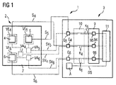
- 検出装置(2)と調整装置(3)を備えたビーム検出器(1)であって、
当該検出装置は多数の検出器部材(4、5、6)を有しており、
前記ビーム検出器の作動時に当該検出器部材によって検出器信号(DS)が得られ、
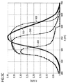
・前記検出器部材はそれぞれ1つのスペクトル感度分布(400、500、600)を有しており、信号形成(S4、S5、S6)に適しており、
・少なくとも1つの検出器部材は化合物半導体材料を含んでおり、かつ当該検出器部材は可視スペクトル領域におけるビームを検出するために構成されており、
・前記検出器部材の感度分布によって、ビーム検出器の種々異なるスペクトル感度チャネル(420、520、620)が形成されるように、前記ビーム検出器が構成されており、
・前記感度チャネルにおいて、前記検出器部材によって、各感度チャネルに割り当てられたチャネル信号(K4、K5、K6)が形成され、
・種々異なるチャネル信号の、ビーム検出器の検出信号に対する関与が異なって調整されるように、前記調整装置が構成されている、
ことを特徴とするビーム検出器。 - 前記調整装置は、チャネル信号の、検出信号に対する関与を相対的に相互に異なって重み付けする、請求項1記載のビーム検出器。
- 前記ビーム検出器の検出器信号は、チャネル信号の重畳によって構成されている、請求項1または2記載のビーム検出器。
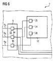
- 前記調整装置は多数の入力側(E4、E5、E6)を有しており、当該入力側を介して、前記検出器部材内で形成された信号が調整装置に入力され、種々の入力側に種々異なる検出器部材が割り当てられている、請求項1から3までの少なくとも1項記載のビーム検出器。
- 前記調整装置は多数の調整端子(94、95、96)を有しており、当該調整端子を介して、検出器信号に対するチャネル信号の関与が調整可能である、請求項1から4までの少なくとも1項記載のビーム検出器。
- 個々のチャネル信号は、異なる検出部材において生成された2つの信号によって得られる、請求項1から5までの少なくとも1項記載のビーム検出器。
- チャネル信号は、異なる2つの検出器部材において生成された信号の差(10)を形成して得られる、請求項1から6までの少なくとも1項記載のビーム検出器。
- 前記感度チャネルはスペクトル的に重畳している、請求項1から7までの少なくとも1項記載のビーム検出器。
- 前記感度チャネルは、可視スペクトル領域が覆われるように重畳している、請求項1から8までの少なくとも1項記載のビーム検出器。
- 前記ビーム検出器が、人間の眼のスペクトル分布(700、702)に相応する検出器感度のスペクトル分布を備えた周辺光センサとして作動可能であるように前記調整装置は構成されている、請求項1から9までの少なくとも1項記載のビーム検出器。
- 前記検出器感度のスペクトル分布は、調整装置によって、明順応している人間の眼のスペクトル分布(700)と暗順応している人間の眼のスペクトル分布(702)の間で切り換え可能である、請求項10記載のビーム検出器。
- 色センサとして、殊に3つの原色、例えば赤、緑および青を検出するために作動可能である、請求項1から11までの少なくとも1項記載のビーム検出器。
- 前記調整装置によって、周辺光センサとしても色センサとして作動可能である、請求項12および請求項10または請求項10にかかる請求項のいずれか1項記載のビーム検出器。
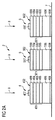
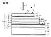
- 前記検出装置は、殊にエピタキシャル成長された半導体ボディ(200、401、501、601)を有しており、前記半導体ボディは少なくとも1つの検出器部材を含んでいる、請求項1から13までの少なくとも1項記載のビーム検出器。
- 前記検出器部材は、信号形成に用いられる活性領域(403、503、603)を有しており、当該活性領域は化合物半導体材料を含んでいる、請求項14記載のビーム検出器。
- 多数の検出器部材はモノリシックに、共通の半導体ボディ(200)内に集積されている、請求項14または15記載のビーム検出器。
- 別個に分けられ、相互に隣り合って配置されている多数の検出器部材を有している、請求項1から16までの少なくとも1項記載のビーム検出器。
- 多数の検出器部材は化合物半導体材料を含んでいる、請求項1から17までの少なくとも1項記載のビーム検出器。
- 多数の検出器部材は、可視のスペクトル領域にあるビームを検出するために構成されている、請求項1から18までの少なくとも1項記載のビーム検出器。
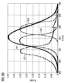
- 3つ以上、有利には4つ以上、特に有利には5つ以上の感度チャネルを有している、請求項1から19までの少なくとも1項記載のビーム検出器。
- 1つまたは多数の狭帯域の感度チャネル(801・・・809)を有している、請求項1から20までの少なくとも1項記載のビーム検出器。
- 前記化合物半導体材料はIII−V−族半導体材料、有利には材料系(In、Al、Ga)Pからの化合物半導体材料である、請求項1から21までの少なくとも1項記載のビーム検出器。
- 前記調整装置は、集積回路として構成されている、請求項1から22までの少なくとも1項記載のビーム検出器。
Applications Claiming Priority (3)
| Application Number | Priority Date | Filing Date | Title |
|---|---|---|---|
| DE102006056579 | 2006-11-30 | ||
| DE102007012115A DE102007012115A1 (de) | 2006-11-30 | 2007-03-13 | Strahlungsdetektor |
| PCT/EP2007/063007 WO2008065170A1 (de) | 2006-11-30 | 2007-11-29 | Strahlungsdetektor mit einstellbarer spektraler empfindlichkeit |
Publications (2)
| Publication Number | Publication Date |
|---|---|
| JP2010511162A true JP2010511162A (ja) | 2010-04-08 |
| JP2010511162A5 JP2010511162A5 (ja) | 2011-10-13 |
Family
ID=39110400
Family Applications (1)
| Application Number | Title | Priority Date | Filing Date |
|---|---|---|---|
| JP2009538716A Pending JP2010511162A (ja) | 2006-11-30 | 2007-11-29 | 調整可能なスペクトル感度を備えたビーム検出器 |
Country Status (8)
| Country | Link |
|---|---|
| US (1) | US8274657B2 (ja) |
| EP (1) | EP2054705A1 (ja) |
| JP (1) | JP2010511162A (ja) |
| KR (1) | KR101430030B1 (ja) |
| CN (1) | CN101535785B (ja) |
| DE (1) | DE102007012115A1 (ja) |
| TW (1) | TWI365976B (ja) |
| WO (1) | WO2008065170A1 (ja) |
Cited By (1)
| Publication number | Priority date | Publication date | Assignee | Title |
|---|---|---|---|---|
| WO2022003813A1 (ja) * | 2020-06-30 | 2022-01-06 | シャープ株式会社 | 電磁波センサ装置および表示装置 |
Families Citing this family (26)
| Publication number | Priority date | Publication date | Assignee | Title |
|---|---|---|---|---|
| US7442629B2 (en) | 2004-09-24 | 2008-10-28 | President & Fellows Of Harvard College | Femtosecond laser-induced formation of submicrometer spikes on a semiconductor substrate |
| US7057256B2 (en) | 2001-05-25 | 2006-06-06 | President & Fellows Of Harvard College | Silicon-based visible and near-infrared optoelectric devices |
| US7890055B1 (en) * | 2007-07-09 | 2011-02-15 | Everlokt Corporation | Touch field compound field detector personal ID |
| JP2010112808A (ja) * | 2008-11-05 | 2010-05-20 | Hioki Ee Corp | 光パワーメータ |
| JP2010112807A (ja) * | 2008-11-05 | 2010-05-20 | Hioki Ee Corp | 光パワーメータ |
| US8008613B2 (en) | 2009-05-05 | 2011-08-30 | Apple Inc. | Light sensing device having a color sensor and a clear sensor for infrared rejection |
| DE102009024069A1 (de) | 2009-06-05 | 2010-12-09 | Osram Opto Semiconductors Gmbh | Optisches Beleuchtungsgerät und optisches Aufzeichnungsgerät |
| US9673243B2 (en) | 2009-09-17 | 2017-06-06 | Sionyx, Llc | Photosensitive imaging devices and associated methods |
| KR102234065B1 (ko) * | 2009-09-17 | 2021-03-31 | 사이오닉스, 엘엘씨 | 감광성 이미징 장치 및 이와 관련된 방법 |
| US9911781B2 (en) | 2009-09-17 | 2018-03-06 | Sionyx, Llc | Photosensitive imaging devices and associated methods |
| EP2487509A4 (en) * | 2009-10-05 | 2015-06-17 | Shimadzu Corp | RADIATION DETECTOR |
| US8692198B2 (en) | 2010-04-21 | 2014-04-08 | Sionyx, Inc. | Photosensitive imaging devices and associated methods |
| WO2011160130A2 (en) | 2010-06-18 | 2011-12-22 | Sionyx, Inc | High speed photosensitive devices and associated methods |
| EP2684221A4 (en) | 2011-03-10 | 2014-08-20 | Sionyx Inc | THREE-DIMENSIONAL SENSORS, SYSTEMS AND RELATED METHODS |
| WO2012130280A1 (de) | 2011-03-29 | 2012-10-04 | Osram Opto Semiconductors Gmbh | Einheit zur bestimmung der art einer dominierenden lichtquelle mittels zweier fotodioden |
| US9496308B2 (en) | 2011-06-09 | 2016-11-15 | Sionyx, Llc | Process module for increasing the response of backside illuminated photosensitive imagers and associated methods |
| JP2014525091A (ja) | 2011-07-13 | 2014-09-25 | サイオニクス、インク. | 生体撮像装置および関連方法 |
| US8865507B2 (en) | 2011-09-16 | 2014-10-21 | Sionyx, Inc. | Integrated visible and infrared imager devices and associated methods |
| US9064764B2 (en) | 2012-03-22 | 2015-06-23 | Sionyx, Inc. | Pixel isolation elements, devices, and associated methods |
| KR20150130303A (ko) | 2013-02-15 | 2015-11-23 | 사이오닉스, 아이엔씨. | 안티 블루밍 특성 및 관련 방법을 가지는 높은 동적 범위의 cmos 이미지 센서 |
| US9939251B2 (en) | 2013-03-15 | 2018-04-10 | Sionyx, Llc | Three dimensional imaging utilizing stacked imager devices and associated methods |
| US9209345B2 (en) | 2013-06-29 | 2015-12-08 | Sionyx, Inc. | Shallow trench textured regions and associated methods |
| US10281329B2 (en) * | 2017-06-14 | 2019-05-07 | Simmonds Precision Products, Inc. | Method and system for fast determination of the wavelength of a light beam |
| CN109556710B (zh) * | 2018-12-28 | 2024-04-16 | 浙江智慧照明技术有限公司 | 照明环境光传感器 |
| DE102019114537A1 (de) * | 2019-05-29 | 2020-12-03 | OSRAM Opto Semiconductors Gesellschaft mit beschränkter Haftung | Optoelektronisches sensorbauelement zur lichtmessung mit eingebauter redundanz |
| KR102774244B1 (ko) * | 2019-11-19 | 2025-03-05 | 삼성전자주식회사 | 스펙트럼을 분할하는 발광 소자 측정 장치, 및 이의 동작 방법 |
Citations (9)
| Publication number | Priority date | Publication date | Assignee | Title |
|---|---|---|---|---|
| DE2920773A1 (de) * | 1979-05-22 | 1980-12-04 | Siemens Ag | Optoelektronischer sensor |
| JPS6336121A (ja) * | 1986-07-29 | 1988-02-16 | Minolta Camera Co Ltd | 測色センサ |
| JPH01233328A (ja) * | 1988-03-14 | 1989-09-19 | Agency Of Ind Science & Technol | 測光装置 |
| JPH03202732A (ja) * | 1989-06-13 | 1991-09-04 | Sharp Corp | カラーセンサ |
| JP2000066166A (ja) * | 1998-08-21 | 2000-03-03 | Mitsubishi Electric Corp | 投写型液晶表示装置 |
| DE10101457A1 (de) * | 2001-01-10 | 2002-07-18 | Infineon Technologies Ag | Optoelektronisches System zur Detektion elektromagnetischer Strahlung |
| EP1521069A2 (de) * | 2003-10-02 | 2005-04-06 | MAZet GmbH | Photosensor zur normgerechten Farbmessung |
| JP2006108675A (ja) * | 2004-09-30 | 2006-04-20 | Osram Opto Semiconductors Gmbh | ビーム検出器 |
| JP2006189291A (ja) * | 2005-01-05 | 2006-07-20 | Konica Minolta Sensing Inc | 測光装置及び単色光の測光方法 |
Family Cites Families (25)
| Publication number | Priority date | Publication date | Assignee | Title |
|---|---|---|---|---|
| JPS55104725A (en) | 1979-02-05 | 1980-08-11 | Nec Corp | Wave-length discrimination type photo-detector |
| JPS59227171A (ja) | 1983-06-08 | 1984-12-20 | Oki Electric Ind Co Ltd | カラ−センサ |
| US4758734A (en) | 1984-03-13 | 1988-07-19 | Nec Corporation | High resolution image sensor array using amorphous photo-diodes |
| JPH0612808B2 (ja) | 1984-07-13 | 1994-02-16 | 日本電気株式会社 | 固体撮像装置の製造方法 |
| DE4024011A1 (de) * | 1990-07-28 | 1992-01-30 | Gossen Gmbh | Verfahren und vorrichtung zur elektronischen belichtungsmessung |
| JPH04280678A (ja) | 1991-03-08 | 1992-10-06 | Nec Corp | 固体撮像素子 |
| DE4143284A1 (de) | 1991-12-30 | 1992-10-01 | Klaus Eberhard Engel | Integrierter halbleitersensor fuer spektrometer |
| GB2277405A (en) | 1993-04-22 | 1994-10-26 | Sharp Kk | Semiconductor colour display or detector array |
| US5362969A (en) | 1993-04-23 | 1994-11-08 | Luxtron Corporation | Processing endpoint detecting technique and detector structure using multiple radiation sources or discrete detectors |
| EP0645826A3 (en) | 1993-09-23 | 1995-05-17 | Siemens Comp Inc | Monolithic multi-channel optocoupler. |
| US5926282A (en) | 1995-09-27 | 1999-07-20 | Fraunhofer-Gesellschaft Zur Forderung Der Angewandten Forschung E.V. | Multispectral sensor device |
| CA2171574C (en) * | 1996-03-12 | 2000-10-03 | Brian W. Tansley | Photometric measurement apparatus |
| US6307660B1 (en) | 1997-01-28 | 2001-10-23 | Tellium, Inc. | Optical receiver particularly useful for a multi-wavelength receiver array |
| US6359274B1 (en) | 1999-01-25 | 2002-03-19 | Gentex Corporation | Photodiode light sensor |
| US6407439B1 (en) | 1999-08-19 | 2002-06-18 | Epitaxial Technologies, Llc | Programmable multi-wavelength detector array |
| US7065035B1 (en) | 1999-10-25 | 2006-06-20 | Matsushita Electric Industrial Co., Ltd. | Optical multilayer disk, multiwavelength light source, and optical system using them |
| US6380532B1 (en) | 2000-04-19 | 2002-04-30 | Eaton Corporation | Optical object detector with multiple photodetectors |
| GB2381950A (en) | 2001-11-06 | 2003-05-14 | Denselight Semiconductors Pte | Field effect based photodetector array responsivity control |
| TW499577B (en) | 2001-12-07 | 2002-08-21 | Univ Yuan Ze | Coiled optical fiber wavelength - power converter |
| DE10345410A1 (de) | 2003-09-30 | 2005-05-04 | Osram Opto Semiconductors Gmbh | Strahlungsdetektor |
| DE102004037020B4 (de) * | 2003-09-30 | 2021-10-21 | OSRAM Opto Semiconductors Gesellschaft mit beschränkter Haftung | Strahlungsdetektor zur Detektion von Strahlung gemäß einer vorgegebenen spektralen Empfindlichkeitsverteilung |
| US8212285B2 (en) | 2004-03-31 | 2012-07-03 | Osram Opto Semiconductors Gmbh | Radiation detector |
| DE102005001280B4 (de) * | 2004-09-30 | 2022-03-03 | OSRAM Opto Semiconductors Gesellschaft mit beschränkter Haftung | Strahlungsdetektor |
| EP1667246A1 (en) * | 2004-12-03 | 2006-06-07 | ETeCH AG | A multi-colour sensitive device for colour image sensing |
| DE102005043918B4 (de) | 2005-05-30 | 2014-12-04 | Osram Opto Semiconductors Gmbh | Detektoranordnung und Verfahren zur Bestimmung spektraler Anteile in einer auf eine Detektoranordnung einfallenden Strahlung |
-
2007
- 2007-03-13 DE DE102007012115A patent/DE102007012115A1/de not_active Ceased
- 2007-11-26 TW TW096144735A patent/TWI365976B/zh active
- 2007-11-29 JP JP2009538716A patent/JP2010511162A/ja active Pending
- 2007-11-29 KR KR1020097013679A patent/KR101430030B1/ko active Active
- 2007-11-29 CN CN2007800414217A patent/CN101535785B/zh active Active
- 2007-11-29 EP EP07847523A patent/EP2054705A1/de not_active Ceased
- 2007-11-29 US US12/516,831 patent/US8274657B2/en active Active
- 2007-11-29 WO PCT/EP2007/063007 patent/WO2008065170A1/de not_active Ceased
Patent Citations (9)
| Publication number | Priority date | Publication date | Assignee | Title |
|---|---|---|---|---|
| DE2920773A1 (de) * | 1979-05-22 | 1980-12-04 | Siemens Ag | Optoelektronischer sensor |
| JPS6336121A (ja) * | 1986-07-29 | 1988-02-16 | Minolta Camera Co Ltd | 測色センサ |
| JPH01233328A (ja) * | 1988-03-14 | 1989-09-19 | Agency Of Ind Science & Technol | 測光装置 |
| JPH03202732A (ja) * | 1989-06-13 | 1991-09-04 | Sharp Corp | カラーセンサ |
| JP2000066166A (ja) * | 1998-08-21 | 2000-03-03 | Mitsubishi Electric Corp | 投写型液晶表示装置 |
| DE10101457A1 (de) * | 2001-01-10 | 2002-07-18 | Infineon Technologies Ag | Optoelektronisches System zur Detektion elektromagnetischer Strahlung |
| EP1521069A2 (de) * | 2003-10-02 | 2005-04-06 | MAZet GmbH | Photosensor zur normgerechten Farbmessung |
| JP2006108675A (ja) * | 2004-09-30 | 2006-04-20 | Osram Opto Semiconductors Gmbh | ビーム検出器 |
| JP2006189291A (ja) * | 2005-01-05 | 2006-07-20 | Konica Minolta Sensing Inc | 測光装置及び単色光の測光方法 |
Cited By (1)
| Publication number | Priority date | Publication date | Assignee | Title |
|---|---|---|---|---|
| WO2022003813A1 (ja) * | 2020-06-30 | 2022-01-06 | シャープ株式会社 | 電磁波センサ装置および表示装置 |
Also Published As
| Publication number | Publication date |
|---|---|
| US8274657B2 (en) | 2012-09-25 |
| DE102007012115A1 (de) | 2008-06-05 |
| CN101535785B (zh) | 2011-12-28 |
| KR101430030B1 (ko) | 2014-08-14 |
| WO2008065170A1 (de) | 2008-06-05 |
| US20100097609A1 (en) | 2010-04-22 |
| KR20090098850A (ko) | 2009-09-17 |
| EP2054705A1 (de) | 2009-05-06 |
| TW200844412A (en) | 2008-11-16 |
| CN101535785A (zh) | 2009-09-16 |
| TWI365976B (en) | 2012-06-11 |
Similar Documents
| Publication | Publication Date | Title |
|---|---|---|
| JP2010511162A (ja) | 調整可能なスペクトル感度を備えたビーム検出器 | |
| JP5166687B2 (ja) | ビーム検出器 | |
| US8803270B2 (en) | Light sensor having IR cut and color pass interference filter integrated on-chip | |
| US7248297B2 (en) | Integrated color pixel (ICP) | |
| US7329895B2 (en) | Dual wavelength detector | |
| US7858921B2 (en) | Guided-mode-resonance transmission color filters for color generation in CMOS image sensors | |
| JP6509782B2 (ja) | 画像センサ、前記画像センサを備える光電子システム、および前記画像センサを製造するための方法 | |
| TWI357494B (en) | Photodetector having dark current correction | |
| US6580089B2 (en) | Multi-quantum-well infrared sensor array in spatially-separated multi-band configuration | |
| WO2017058109A1 (en) | Optoelectronic modules for the acquisition of spectral and distance data | |
| US20130309803A1 (en) | Radiation sensor with photodiodes being integrated on a semiconductor substrate and corresponding integration process | |
| JP7758298B2 (ja) | ダブル・フォトダイオード電磁放射センサ・デバイス | |
| KR20100109563A (ko) | 복사 수신기 및 복사 수신기의 제조 방법 | |
| KR20180071192A (ko) | 이미지 센서 및 이를 포함하는 전자 장치 | |
| US20080237633A1 (en) | Radiation Detector | |
| CN101981696B (zh) | 光电射线检测器和用于制造多个检测器元件的方法 | |
| US20080105820A1 (en) | Resonant structures for electromagnetic energy detection system and associated methods | |
| JPH0555622A (ja) | 半導体受光装置 | |
| TWI376784B (en) | Detector arrangement and detector component | |
| KR20100079452A (ko) | 이미지센서 | |
| Lee et al. | Highly sensitive gate/body-tied metaloxide-semiconductor field-effect transistor-type photodetector with wavelength-selective metal grid structure using standard complementary metal-oxide-semiconductor technology | |
| JPH01282875A (ja) | カラーセンサ | |
| CN121080142A (zh) | 具有可在光伏模式下操作的光电二极管的电磁辐射传感器器件 | |
| JPH03278476A (ja) | 光センサ |
Legal Events
| Date | Code | Title | Description |
|---|---|---|---|
| A621 | Written request for application examination |
Free format text: JAPANESE INTERMEDIATE CODE: A621 Effective date: 20100809 |
|
| RD04 | Notification of resignation of power of attorney |
Free format text: JAPANESE INTERMEDIATE CODE: A7424 Effective date: 20101228 |
|
| A521 | Request for written amendment filed |
Free format text: JAPANESE INTERMEDIATE CODE: A523 Effective date: 20110823 |
|
| A977 | Report on retrieval |
Free format text: JAPANESE INTERMEDIATE CODE: A971007 Effective date: 20120524 |
|
| A131 | Notification of reasons for refusal |
Free format text: JAPANESE INTERMEDIATE CODE: A131 Effective date: 20120530 |
|
| A601 | Written request for extension of time |
Free format text: JAPANESE INTERMEDIATE CODE: A601 Effective date: 20120829 |
|
| A602 | Written permission of extension of time |
Free format text: JAPANESE INTERMEDIATE CODE: A602 Effective date: 20120905 |
|
| A521 | Request for written amendment filed |
Free format text: JAPANESE INTERMEDIATE CODE: A523 Effective date: 20121001 |
|
| A02 | Decision of refusal |
Free format text: JAPANESE INTERMEDIATE CODE: A02 Effective date: 20130201 |