EP1667246A1 - A multi-colour sensitive device for colour image sensing - Google Patents
A multi-colour sensitive device for colour image sensing Download PDFInfo
- Publication number
- EP1667246A1 EP1667246A1 EP04028707A EP04028707A EP1667246A1 EP 1667246 A1 EP1667246 A1 EP 1667246A1 EP 04028707 A EP04028707 A EP 04028707A EP 04028707 A EP04028707 A EP 04028707A EP 1667246 A1 EP1667246 A1 EP 1667246A1
- Authority
- EP
- European Patent Office
- Prior art keywords
- sensor element
- element according
- electromagnetic radiation
- sub
- colour
- Prior art date
- Legal status (The legal status is an assumption and is not a legal conclusion. Google has not performed a legal analysis and makes no representation as to the accuracy of the status listed.)
- Withdrawn
Links
- 239000004065 semiconductor Substances 0.000 claims abstract description 41
- 230000003595 spectral effect Effects 0.000 claims abstract description 34
- 230000005670 electromagnetic radiation Effects 0.000 claims abstract description 30
- XUIMIQQOPSSXEZ-UHFFFAOYSA-N Silicon Chemical compound [Si] XUIMIQQOPSSXEZ-UHFFFAOYSA-N 0.000 claims abstract description 8
- 229910052710 silicon Inorganic materials 0.000 claims abstract description 8
- 239000010703 silicon Substances 0.000 claims abstract description 8
- GWEVSGVZZGPLCZ-UHFFFAOYSA-N Titan oxide Chemical compound O=[Ti]=O GWEVSGVZZGPLCZ-UHFFFAOYSA-N 0.000 claims description 38
- 239000000975 dye Substances 0.000 claims description 38
- 230000035945 sensitivity Effects 0.000 claims description 15
- 239000000463 material Substances 0.000 claims description 13
- XOLBLPGZBRYERU-UHFFFAOYSA-N tin dioxide Chemical compound O=[Sn]=O XOLBLPGZBRYERU-UHFFFAOYSA-N 0.000 claims description 9
- DZVCFNFOPIZQKX-LTHRDKTGSA-M merocyanine Chemical compound [Na+].O=C1N(CCCC)C(=O)N(CCCC)C(=O)C1=C\C=C\C=C/1N(CCCS([O-])(=O)=O)C2=CC=CC=C2O\1 DZVCFNFOPIZQKX-LTHRDKTGSA-M 0.000 claims description 7
- 229910001887 tin oxide Inorganic materials 0.000 claims description 7
- 230000000694 effects Effects 0.000 claims description 6
- 239000003792 electrolyte Substances 0.000 claims description 6
- 239000004408 titanium dioxide Substances 0.000 claims description 5
- 238000001228 spectrum Methods 0.000 claims description 4
- KJTLSVCANCCWHF-UHFFFAOYSA-N Ruthenium Chemical compound [Ru] KJTLSVCANCCWHF-UHFFFAOYSA-N 0.000 claims description 3
- 206010070834 Sensitisation Diseases 0.000 claims description 3
- ZYGHJZDHTFUPRJ-UHFFFAOYSA-N coumarin Chemical compound C1=CC=C2OC(=O)C=CC2=C1 ZYGHJZDHTFUPRJ-UHFFFAOYSA-N 0.000 claims description 3
- 229910052731 fluorine Inorganic materials 0.000 claims description 3
- 239000011737 fluorine Substances 0.000 claims description 3
- 239000002096 quantum dot Substances 0.000 claims description 3
- 229910052707 ruthenium Inorganic materials 0.000 claims description 3
- 230000008313 sensitization Effects 0.000 claims description 3
- 238000012163 sequencing technique Methods 0.000 claims description 3
- IHXWECHPYNPJRR-UHFFFAOYSA-N 3-hydroxycyclobut-2-en-1-one Chemical compound OC1=CC(=O)C1 IHXWECHPYNPJRR-UHFFFAOYSA-N 0.000 claims description 2
- SIKJAQJRHWYJAI-UHFFFAOYSA-N Indole Chemical compound C1=CC=C2NC=CC2=C1 SIKJAQJRHWYJAI-UHFFFAOYSA-N 0.000 claims description 2
- 125000004424 polypyridyl Polymers 0.000 claims description 2
- ANRHNWWPFJCPAZ-UHFFFAOYSA-M thionine Chemical compound [Cl-].C1=CC(N)=CC2=[S+]C3=CC(N)=CC=C3N=C21 ANRHNWWPFJCPAZ-UHFFFAOYSA-M 0.000 claims description 2
- 230000002596 correlated effect Effects 0.000 claims 1
- 230000003247 decreasing effect Effects 0.000 claims 1
- 125000001153 fluoro group Chemical group F* 0.000 claims 1
- 230000001788 irregular Effects 0.000 claims 1
- 150000003839 salts Chemical class 0.000 claims 1
- 230000005641 tunneling Effects 0.000 claims 1
- 239000010410 layer Substances 0.000 description 91
- 230000004044 response Effects 0.000 description 27
- 238000010521 absorption reaction Methods 0.000 description 21
- 239000000758 substrate Substances 0.000 description 17
- 238000003491 array Methods 0.000 description 9
- 239000011521 glass Substances 0.000 description 8
- 238000003384 imaging method Methods 0.000 description 6
- 239000004020 conductor Substances 0.000 description 5
- 238000009826 distribution Methods 0.000 description 5
- 238000000034 method Methods 0.000 description 5
- 238000000862 absorption spectrum Methods 0.000 description 4
- 238000004519 manufacturing process Methods 0.000 description 4
- 230000003287 optical effect Effects 0.000 description 4
- 239000002245 particle Substances 0.000 description 4
- 239000001045 blue dye Substances 0.000 description 3
- 230000035515 penetration Effects 0.000 description 3
- LFQSCWFLJHTTHZ-UHFFFAOYSA-N Ethanol Chemical compound CCO LFQSCWFLJHTTHZ-UHFFFAOYSA-N 0.000 description 2
- YCKRFDGAMUMZLT-UHFFFAOYSA-N Fluorine atom Chemical compound [F] YCKRFDGAMUMZLT-UHFFFAOYSA-N 0.000 description 2
- 230000001476 alcoholic effect Effects 0.000 description 2
- 230000008901 benefit Effects 0.000 description 2
- 230000005540 biological transmission Effects 0.000 description 2
- 238000006243 chemical reaction Methods 0.000 description 2
- 239000003086 colorant Substances 0.000 description 2
- 230000007423 decrease Effects 0.000 description 2
- 238000001514 detection method Methods 0.000 description 2
- 239000001046 green dye Substances 0.000 description 2
- 239000012212 insulator Substances 0.000 description 2
- HSZCZNFXUDYRKD-UHFFFAOYSA-M lithium iodide Chemical compound [Li+].[I-] HSZCZNFXUDYRKD-UHFFFAOYSA-M 0.000 description 2
- BASFCYQUMIYNBI-UHFFFAOYSA-N platinum Chemical compound [Pt] BASFCYQUMIYNBI-UHFFFAOYSA-N 0.000 description 2
- 239000011148 porous material Substances 0.000 description 2
- 230000005855 radiation Effects 0.000 description 2
- 239000001044 red dye Substances 0.000 description 2
- 239000000243 solution Substances 0.000 description 2
- 238000001429 visible spectrum Methods 0.000 description 2
- ZCYVEMRRCGMTRW-UHFFFAOYSA-N 7553-56-2 Chemical compound [I] ZCYVEMRRCGMTRW-UHFFFAOYSA-N 0.000 description 1
- ATJFFYVFTNAWJD-UHFFFAOYSA-N Tin Chemical compound [Sn] ATJFFYVFTNAWJD-UHFFFAOYSA-N 0.000 description 1
- YIYFFLYGSHJWFF-UHFFFAOYSA-N [Zn].N1C(C=C2N=C(C=C3NC(=C4)C=C3)C=C2)=CC=C1C=C1C=CC4=N1 Chemical compound [Zn].N1C(C=C2N=C(C=C3NC(=C4)C=C3)C=C2)=CC=C1C=C1C=CC4=N1 YIYFFLYGSHJWFF-UHFFFAOYSA-N 0.000 description 1
- 239000011149 active material Substances 0.000 description 1
- 238000000149 argon plasma sintering Methods 0.000 description 1
- 238000000151 deposition Methods 0.000 description 1
- 230000008021 deposition Effects 0.000 description 1
- 238000005516 engineering process Methods 0.000 description 1
- 230000005284 excitation Effects 0.000 description 1
- 238000002474 experimental method Methods 0.000 description 1
- 238000001914 filtration Methods 0.000 description 1
- 239000003574 free electron Substances 0.000 description 1
- 238000005286 illumination Methods 0.000 description 1
- 238000005470 impregnation Methods 0.000 description 1
- 230000006872 improvement Effects 0.000 description 1
- 238000002190 incident photon conversion efficiency spectrum Methods 0.000 description 1
- 238000002347 injection Methods 0.000 description 1
- 239000007924 injection Substances 0.000 description 1
- 230000010354 integration Effects 0.000 description 1
- 230000002452 interceptive effect Effects 0.000 description 1
- 229910052740 iodine Inorganic materials 0.000 description 1
- 239000011630 iodine Substances 0.000 description 1
- 239000011244 liquid electrolyte Substances 0.000 description 1
- 239000003960 organic solvent Substances 0.000 description 1
- 238000000059 patterning Methods 0.000 description 1
- 229910052697 platinum Inorganic materials 0.000 description 1
- 230000008569 process Effects 0.000 description 1
- 238000005215 recombination Methods 0.000 description 1
- 230000006798 recombination Effects 0.000 description 1
- 238000013341 scale-up Methods 0.000 description 1
- 238000007789 sealing Methods 0.000 description 1
- 238000000926 separation method Methods 0.000 description 1
- 239000002356 single layer Substances 0.000 description 1
- 239000007784 solid electrolyte Substances 0.000 description 1
- 238000005118 spray pyrolysis Methods 0.000 description 1
- 239000000126 substance Substances 0.000 description 1
- 230000007704 transition Effects 0.000 description 1
- 238000000825 ultraviolet detection Methods 0.000 description 1
- 229910052724 xenon Inorganic materials 0.000 description 1
- FHNFHKCVQCLJFQ-UHFFFAOYSA-N xenon atom Chemical compound [Xe] FHNFHKCVQCLJFQ-UHFFFAOYSA-N 0.000 description 1
Images


Classifications
-
- H—ELECTRICITY
- H01—ELECTRIC ELEMENTS
- H01L—SEMICONDUCTOR DEVICES NOT COVERED BY CLASS H10
- H01L31/00—Semiconductor devices sensitive to infrared radiation, light, electromagnetic radiation of shorter wavelength or corpuscular radiation and specially adapted either for the conversion of the energy of such radiation into electrical energy or for the control of electrical energy by such radiation; Processes or apparatus specially adapted for the manufacture or treatment thereof or of parts thereof; Details thereof
- H01L31/08—Semiconductor devices sensitive to infrared radiation, light, electromagnetic radiation of shorter wavelength or corpuscular radiation and specially adapted either for the conversion of the energy of such radiation into electrical energy or for the control of electrical energy by such radiation; Processes or apparatus specially adapted for the manufacture or treatment thereof or of parts thereof; Details thereof in which radiation controls flow of current through the device, e.g. photoresistors
- H01L31/10—Semiconductor devices sensitive to infrared radiation, light, electromagnetic radiation of shorter wavelength or corpuscular radiation and specially adapted either for the conversion of the energy of such radiation into electrical energy or for the control of electrical energy by such radiation; Processes or apparatus specially adapted for the manufacture or treatment thereof or of parts thereof; Details thereof in which radiation controls flow of current through the device, e.g. photoresistors characterised by at least one potential-jump barrier or surface barrier, e.g. phototransistors
- H01L31/101—Devices sensitive to infrared, visible or ultraviolet radiation
-
- B—PERFORMING OPERATIONS; TRANSPORTING
- B82—NANOTECHNOLOGY
- B82Y—SPECIFIC USES OR APPLICATIONS OF NANOSTRUCTURES; MEASUREMENT OR ANALYSIS OF NANOSTRUCTURES; MANUFACTURE OR TREATMENT OF NANOSTRUCTURES
- B82Y10/00—Nanotechnology for information processing, storage or transmission, e.g. quantum computing or single electron logic
-
- H—ELECTRICITY
- H01—ELECTRIC ELEMENTS
- H01G—CAPACITORS; CAPACITORS, RECTIFIERS, DETECTORS, SWITCHING DEVICES OR LIGHT-SENSITIVE DEVICES, OF THE ELECTROLYTIC TYPE
- H01G9/00—Electrolytic capacitors, rectifiers, detectors, switching devices, light-sensitive or temperature-sensitive devices; Processes of their manufacture
- H01G9/20—Light-sensitive devices
- H01G9/2068—Panels or arrays of photoelectrochemical cells, e.g. photovoltaic modules based on photoelectrochemical cells
- H01G9/2072—Panels or arrays of photoelectrochemical cells, e.g. photovoltaic modules based on photoelectrochemical cells comprising two or more photoelectrodes sensible to different parts of the solar spectrum, e.g. tandem cells
-
- H—ELECTRICITY
- H01—ELECTRIC ELEMENTS
- H01L—SEMICONDUCTOR DEVICES NOT COVERED BY CLASS H10
- H01L27/00—Devices consisting of a plurality of semiconductor or other solid-state components formed in or on a common substrate
- H01L27/14—Devices consisting of a plurality of semiconductor or other solid-state components formed in or on a common substrate including semiconductor components sensitive to infrared radiation, light, electromagnetic radiation of shorter wavelength or corpuscular radiation and specially adapted either for the conversion of the energy of such radiation into electrical energy or for the control of electrical energy by such radiation
- H01L27/144—Devices controlled by radiation
- H01L27/146—Imager structures
- H01L27/14643—Photodiode arrays; MOS imagers
- H01L27/14645—Colour imagers
- H01L27/14647—Multicolour imagers having a stacked pixel-element structure, e.g. npn, npnpn or MQW elements
-
- Y—GENERAL TAGGING OF NEW TECHNOLOGICAL DEVELOPMENTS; GENERAL TAGGING OF CROSS-SECTIONAL TECHNOLOGIES SPANNING OVER SEVERAL SECTIONS OF THE IPC; TECHNICAL SUBJECTS COVERED BY FORMER USPC CROSS-REFERENCE ART COLLECTIONS [XRACs] AND DIGESTS
- Y02—TECHNOLOGIES OR APPLICATIONS FOR MITIGATION OR ADAPTATION AGAINST CLIMATE CHANGE
- Y02E—REDUCTION OF GREENHOUSE GAS [GHG] EMISSIONS, RELATED TO ENERGY GENERATION, TRANSMISSION OR DISTRIBUTION
- Y02E10/00—Energy generation through renewable energy sources
- Y02E10/50—Photovoltaic [PV] energy
- Y02E10/542—Dye sensitized solar cells
Definitions
- 'colour detection' is normally synonymous with 'visible electromagnetic radiation detection'
- this method can also be used to gain information on the spectral distribution of electromagnetic radiation outside the range of visible light (e.g. ultraviolet, infrared or x-ray), using filter layers with the according transmission properties.
- the semiconductor can be patterned to provide many individual photo sensors on a single substrate, and the colour filter can be likewise pattered to the same (x-y) dimensions. If it is desired to sense more than one colour with the same photo sensor substrate, particularly to capture a colour image, conventionally the colour filter is patterned with a pixel (picture-point) array of different colour filters, which conventionally control the light transmitted through the filter to adjacent photo sensors. Using pixel elements with different color filters next to each other in a two-dimensional array makes it possible to provide color information for the image detected. Sensing devices applying color filters generally consist of sensor elements lying side-by-side on a sensor plain. Using the response of neighboring pixel elements with different sensitivities (typically three to four) it is possible to measure light intensity as well as the spectral distribution of light at a given point.
- the size of one pixel for which full colour information is known is (by area) at least three times greater than the size of the corresponding photo sensor elements: or, to express this in a different way, the areal colour resolution of the colour image detector is at best a third of that which would be achievable for a black-and-white image using the same photosensitive detector array.
- a pixel of picture-point an area for which full colour information is directly measured or transmitted and therefore the number of pixels in an array or display is the number for which distinct full colour information is measured (and not interpreted) or transmitted.
- one pixel is an array of 3 to 4 monochrome sub-pixels as mentioned above.
- the creation of the colour filter is far from easy.
- the colour filter has to be deposited with precise evenness at a resolution of typically 1-100 micrometers - which is progressively more difficult to do as the pixel size decreases.
- the regular arrays of colour pixels lead to imaging artifacts termed Moiré patterns.
- a new type of colour image sensor is described where different colours are sensed with the same (x-y) spatial coordinates. This is achieved by using a stack of sensors each of which is sensitive to one colour and transparent to others. This thus allows the creation of a device, composed of such sensing elements, to have high spatial resolution, and avoid certain sensing artifacts, compared with most other known state of the art devices.
- the use of dye-sensitized wide-bandgap semiconductors allows a higher degree of control over the colour sensitivity of the devices than that obtained with other known vertical-stack devices based on doped conventional semiconductors, in particular allowing sensitivity to narrow bands of electromagnetic radiation, and to electromagnetic radiation beyond the human-visible range.
- the present invention allows the colour pixel to be the same size as the sensor pixel, resulting in at least a three-fold improvement in areal resolution for a device of equivalent photo sensor size (or a corresponding decrease in sensor array size for equivalent picture resolution, provided the photo sensor elements may be reduced so far in size; or any suitable compromise between the two, following the definition above). It also, importantly, by removing the conventional patterned colour filters, removes many of the problems with manufacture of colour filters (e.g., achieving evenness, dimensional match to the sensor array, problems with patterning defect-free at this high resolution). It also removes almost all the problems with Moiré patterns.
- such a device to realize sensor arrays that are stacked perpendicular to the imaging plane may also for instance be made practically by using dye-sensitized wide bandgap semiconductor layers.
- semiconductor layers sensitized with different dyes are employed, each of which will select light of one different non-significantly overlapping specific narrow range of wavelengths, and remain transparent to all others.
- the dyes are typically used in combination with a semiconductor, which will only react photosensitively to light when the semiconductor has been sensitized by the dyes. It is also possible to have a distribution of the dye absorption in the different layers according to Fig. 3 and achieve separated and therefore non-significantly overlapping wavelengths responses.
- Dye-sensitized solar cells make use of synthetic or naturally occurring dyes to sensitize wide-bandgap semiconductors such as titanium dioxide to visible light.
- the wide-bandgap semiconductor itself generally exhibits a strong roughness resulting in a high specific surface area.
- the dyes themselves provide the spectral sensitivities - no additional colour filters are required to create sensors with different spectral sensitivities.
- the different spectral sensitivities of individual sensor layers are achieved by the use of different, (in the final result) non-significantly interfering, spectral sensitizers.
- One particular advantage of the present invention is the flexibility it permits in design and manufacture.
- the order of the layers is necessarily fixed in descending wavelength chromatic sequence because it relies on wavelength-related penetration depth; the choice of wavelength of any one layer restricts the wavelength choice of other layers, closely separated wavelengths being impossible to measure because the physical size of the associated structures then prevent certain penetration depths being accessed; wavelengths beyond the human-visible range are not included (possibly an ultra-violet upper layer would be too shallow to construct, and a infra-red layer too deep for a strong enough signal to be sensed, in a single device with fixed dynamic ranges); and the image has to be deconvoluted from the measured signals because the upper layers of the device also measure electromagnetic radiation at wavelengths intended to be measured at the lower levels of the device (i.e., the uppermost 'blue' sensing layer will also absorb and record green and red light).
- the present device has none of the above restrictions.
- the order of the layers is not necessarily fixed in descending chromatic sequence, although this may of course be desirable, because the sensing technology used is not penetration-depth dependant: thus, for instance, a five-layer device measuring infra-red, red, green, blue and ultra-violet signals could be constructed with 120 different possible layer sequences, the optimal one being chosen dependant on the desired results and the sensitivities of the possible layers; and here again, it has to be noted that different dyes could be used to enable different sensitivities to the same narrow wavelength band. Closely spaced wavelength can, if desired, be accurately sensed because the layers do not physically restrict this. Wavelengths beyond the human-visible range are readily detectable with appropriate dyes.
- deconvolution is easier, because although there will be some absorption by the upper layers of wavelengths intended to be measured by the lower layers, this can be avoided to a much greater extent. It also provides that more of the incoming radiation is correctly sensed in the appropriate layers, thus providing a device of greater and more accurate sensitivity as well as improved resolution, which in turn makes reconstruction of a full true-colour image, or whatever false-colour images may be desired, much easier.
- a single sensor element itself is subject matter of claim 1.
- a device containing multiples sensor elements is claimed in claim 14.
- the sensitization is achieved through the use of dyes within the wide-bandgap semiconductors.
- the sensor element is positioned in an array, which is not necessarily a regular array, e.g. a number of sensors can be arranged in different distances one from another.
- the sensor elements can be used for image capture or for non-image capture applications.
- one spectral band is in the human-visible range and in other embodiments a band is in the non-human visible range.
- a preferred embodiment uses the full-colour human visible range.
- Another embodiment uses regular 2D arrays, i.e. direct image capture. Such arrays are not necessarily planar.
- Another embodiment uses regular 1D arrays and scanning techniques, i.e. 'indirect' capture. Such arrays are not necessarily linear.
- a 0D array and scanning techniques are used, i.e. very indirect capture, e.g. a single element of one type, scanning, as part of an array of array of such.
- a first sensor high IR, low IR
- R,G,B second sensor
- a third sensor low UV, high UV
- the stack of sub-elements is parallel, wherein in other embodiments the stack is non-parallel to the front surface, i.e. inclined, circular, spherical, including domed or cylindrical, or parabolic geometries etc..
- a colour sensing image device comprises a plurality of sensors 1.
- One such sensor is shown in Fig. 1 with a schematic cross-sectional view showing the geometry of the layers and contacts.
- Each sensor 1 represents one pixel.
- the colour sensing image device consists preferably of a two-dimensional array of pixels, each one of which is preferably identical, and consists of a number of similar but non-identical layers, as shown in Figure 1 (layers 3, 4, 5, 6, 7, and 8), on top of a substrate 2.
- Said substrate 2 also supports various elements 9 interspersed among the pixels 1.
- the substrate 2 and the elements 9 are structures into which electronic connections 11 and/or active electronic components are embedded to permit addressing of upper layers 3 to 8.
- these contain electronic components of a charge coupled device as known to someone skilled in the art. For sake of simplicity these connections and components are not explained further.
- photosensitive or photoactive layers (layer 3, 5, 7) are deposited onto the substrate 2, separated by insulating layers 4 and 6 deposited alternately with the photosensitive or photoactive layers.
- These photosensitive or photoactive layers 3, 5, and 7 contain a conducting or semiconducting material in which charge is generated upon excitation with electromagnetic radiation. Radiation is either absorbed by the semiconducting or conducting material itself, or preferably by a sensitizer, which sensitizes the generation of charge in the semiconducting or conducting material. Due to the use of different sensitizers or different semiconducting or conducting materials the different layers exhibit different spectral sensitivities towards electromagnetic radiation.
- narrow sensitivity of a lower layer 3 may also comprise and extend to wavelength portions which are already covered by another upper layer, e.g. 5 or 7, because light from said portions of a spectrum will already be absorbed before entering said lower layer, e.g. 3 or 5.
- the photosensitive or photoactive layers 3, 5, and 7 each consists of a porous inorganic semiconductor with an average pore size from 2 - 500 nm.
- the layer may also contain a second medium capable of transporting charge.
- the conductor/semiconductor and the medium preferably form an interpenetrating network.
- this medium is a semiconductor, an organic charge transport material or a solid or liquid electrolyte.
- the photoactive layers are separated by insulating layers (layer 4 and 6). These insulators are preferably porous with an average pore size from 2 - 1000 nm and may contain the same medium as described for layers 3, 5 and 7.
- Element 9 is an insulator positioned on one side of or surrounding the layers 3 to 7 or as shown 8.
- Element 9 hosts electric connections 11, 12 between the photoactive layers and the substrate 2.
- Each photosensitive layer 3, 5, 7 can thereby be addressed via the electronic components or conducting leads 11, 12 of the substrate 2.
- Electrical contact to the medium is thus either provided via direct contact of the medium and an electric connection in the substrate 2 or via element 9: and/or a further layer 8 or layers can be deposited on top of the uppermost sensitive layer which provides electrical contact to the medium, provided that this layer or layers is/are so constituted and/or designed that it does/they do not block access of electromagnetic radiation to the photosensitive layers.
- All layers can hold additional materials, which absorb electromagnetic radiation.
- these materials are optical filter substances.
- pixels 1 as described in Figure 1 in parallel will produce a one or two dimensional array (see Figure 2 with three pixel 20, 21 and 22) - preferably these pixels form a 2-dimensional array which is then useable for imaging purposes. They can be formed on a common substrate 2.
- the present invention can be used for example in a two-dimensional embodiment to directly capture images, as in a charge-coupled device, or in a one-dimensional, preferably linear array, to scan images, as in a colour copier.
- the detector 1 comprises a stack of sub-elements stacked parallel or inclined to the direction of the incoming electromagnetic radiation, which is oriented, in Fig, 1 or 2 as to be oriented vertically to the front surface 8 of the pixel detectors 1, 20, 21 or 22.
- the stack elements can be produced as layers 3, 4, 5, 6, 7 and 8 perpendicular to the main direction of the incident light. However it is also possible to prepare the layers with a lateral step-function, i.e. when the angle of incidence is not perpendicular to the surface of layer 8 but oblique and inclined.
- the layers 4 and 6 are insulating and/or carry the preferably transparent electrodes to be connected with the control unit of the pixel and the device as a whole.
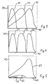
- Fig. 3, 4 and 5 show two embodiments of a distribution of the dyes used for absorption in the different layers according to Fig. 3 and the resulting wavelengths responses.
- Fig. 3 shows a graphic illustration of the absorption 30 for three dyes in dependency on their wavelength 40;
- Fig. 4 shows the signal 41 of the signal responses for a sensor according one embodiment of the invention following Fig. 1 or Fig. 2 against the wavelength 40; and
- Fig. 5 shows the signal 42 of the signal response for a stacked sensor according to prior art or stacked in a non preferred way.
- the reference numerals 31, 32 and 33 designate the absorption curves of three different dyes; from left to right a blue dye, a green dye and a red dye.
- the name of the dyes relates to the main colour component they absorb. It can be seen that the absorption curves 31, 32 and 33 are overlapping.
- the sequence of the different photosensitive layers 3, 5 and 7 comprises the red, the green and the blue dye, respectively.
- Said dyes having the absorption curves 31, 32 and 33, respectively, have the following effect on the transmitted light.
- the uppermost, the blue dye layer 7 with absorption curve 31 absorbs light from said wavelength range, giving as a result the signal response 51 as shown in Fig. 4.
- the not absorbed light i.e. having a greater wavelength (greener and red), travels through layer 6 and enters layer 5.
- the so called green dye layer 5 with absorption curve 32 absorbs light from said wavelength range, giving as a result the signal response 52 as shown in Fig. 4.
- the not absorbed light i.e.
- Fig. 5 now shows another embodiment wherein the colours used within the stacked layers 3, 5 and 7 are inverted, i.e. the uppermost layer is the red layer with the absorption curve 33, followed by the green layer with the absorption curve 32 and finally the bottom layer is the blue layer with the absorption curve 31. Then the signal answers of the different layers are 63, 62 and 61, respectively.
- Quantum dots are small devices that contain a tiny droplet of free electrons. They are fabricated in semiconductor materials and have typical dimensions between nanometers to a few microns. Such sensitization can be reached - but is not limited to - by a thin layer of a narrow bandgap semiconductor or particles of the said narrow bandgap semiconductor deposited on top of the wide bandgap semiconductor with a layer thickness or average particle diameter respectively of typically 1 to 400 nm.
- Thin (3 to 4.5 micrometer) mesoporous films of titanium dioxide were deposited onto conducting glass substrates according to M.K. Nazeeruddin et al., J. Am. Chem. Soc. 115 (1993) 6382.
- the average TiO 2 particle size was 18 nm.
- the so-prepared films were sintered at 450°C for 20 minutes.
- the geometrical surface area of each pixel was 0.28 cm 2 .
- a dense TiO 2 layer (see below for an explanation about the advantages of use of such an additional layer) was deposited onto the conducting glass substrate prior to the deposition of the nanostructured TiO 2 electrode via a spray pyrolysis process described in L. Kavan, M. Graetzel, Electrochimica Acta 40 (1995) 643.
- the thickness of the dense tin layer can be chosen as described in the reference.
- the so-prepared films were immersed into an alcoholic solution (0.5 mg/ml) of different merocyanine dyes as mentioned below for 48 hours at room temperature.
- the dyed TiO 2 electrodes were rinsed with ethanol and dried in air.
- a transparent counter electrode was prepared, consisting of conducting glass and a thin layer of platinum according to N. Papageorgiou, W. F. Maier, M. Graetzel, J. Electrochem Soc. 144 (1997) 876. Closed photoelectrochemical cells were assembled according to P. Wang et al., Nature Materials 2 (2003) 402.
- the electrolyte used contained an organic solvent, 0.5 moles/liter lithium iodide and 0.02 moles/liter iodine.
- IPCE spectral response
- Fig. 6 shows the absorption spectra of mesoporous titanium dioxide films dyed with merocyanine dyes Sc1, Sc2 and Sc3.
- the electrodes were deposited onto conducting glass (fluorine-doped tin(IV)oxide), exposed to an alcoholic solution of the three different merocyanine dyes for 24 hours.
- the three films show distinctively different absorption maxima at 416 nm (Sc1), 509 nm (Sc2) and 548 nm (Sc3).
- Fig. 7 shows the normalized spectral response (IPCE) of individual photoelectrochemical cells assembled from the dye-sensitized TiO 2 films shown in Fig. 6.
- the spectral response generally follows the shape of the absorption spectra with the maxima of the spectral response corresponding to the maxima apparent in the absorption spectra.
- Fig. 8 shows the spectral response of the same cells integrated into a stack as shown in Fig. 9.
- the three cells have received the reference numerals 30, 31 and 32. They comprise a mesoporous core 40, 41 and 42, respectively, with the dyes Sc1, Sc2 and Sc3, respectively.
- the penetration depth of different wave length is shown with arrows 50, 51 and 52, respectively.
- Each cell 30, 31 and 32 has two conducting glass substrates 60 with electrical contacts 61.
- Said dye comprising cores 40, 41 and 42 are mounted on one glass substrate 60 between the two glass substrates 60 of one cell 40, 41 and 42, respectively.
- Sealing elements 62 retain an electrolyte 63 within the confined space between the substrates 60.
- Such a stack is one example of an embodiment with three nearly identical cells, beside the different impregnation of the core 40, 41 and 42 with the dyes Sc1, Sc2 and Sc3, respectively.
- the normalized spectral response of the uppermost cell 30 (with Sc1) is not affected by the underlying stack.
- the normalized spectral response of cell 31 (with Sc2) changes due to the filter layer of the Sc1 cell 30 - especially in the area from 400 to 450 nm, where the normalized spectral response is reduced from above 30 to below 10 % through the overlying Sc1 cell 30.
- the third cell 32 in the stack is most strongly affected by the integration into the stack. Due to the filter effect of top layers the spectral response of the Sc3 cell 32 within the stack changes significantly.
- the stack of cells 30, 31, 32 is sensitive to three distinct wavelength ranges: 400-475 nm; 475-620 nm and 620 to 700 nm.
- the dyes used are such as but not limited to cyanine, merocyanine, phtalocyanine, porphyrine, coumarine, squaraine and/or indoline dyes and/or ruthenium polypyridyl complexes.
- cyanine, merocyanine, phtalocyanine, porphyrine, coumarine, squaraine and/or indoline dyes and/or ruthenium polypyridyl complexes Using non-sensitized TiO 2 it is possible to assemble a UV-sensitive detector because it starts to absorb light at about 400 Nanometer. Ruthenium-dye sensitized photodetectors can detect NIR light up to wavelength of 900 Nanometer. Zinc porphyrine dye shows a strong absorption in the blue and three moderate transitions in the spectral range of 500 to 650 Nanometer.
- Ruthenium N749 so called black dye
- the use of thicker films of such a dye with light scattering particles can be contemplated for the bottom cell in a stack of photosensors.
- Coumarine C343 has a strong absorption band around 400 to 450 Nanometer and a good photon to electron conversion efficiency.
- the invention allows to build nanocrystalline semiconductor electrodes.
- Preferred materials for the sensor are p-type material, redox electrolyte and organic charge transport material.
- the photoresponse can be tuned via the thickness of the sensitized TiO 2 layer.
- the top stack elements show a filter effect, i.e. the thickness of these layers are greater.
- a filter effect between 0,5 and 15 micrometer (equally applicable for the dense tin oxide layer, although a thin thickness is usually sufficient)
- increasing the thickness of the top layer from 2 micrometer to 7 micrometer improves the absorption from 85 to 90 % to more than 99 % thus avoiding potential cross-talk in deeper layers.
- the actual interesting thickness heavily depends on the dye used.
Abstract
A sensor element (1, 20, 21, 22) capable of sensing more than one spectral band of electromagnetic radiation with the same (x-y) spatial location, especially where the dimensions x-y-z form a set of Cartesian coordinates with z parallel to the direction of incident electromagnetic radiation, is characterized in that the element consists of a stack of sub-elements (3, 5, 7) each capable of sensing different spectral bands of electromagnetic radiation. These sub-elements (3, 5, 7) each contain a non-silicon semiconductor where the non-silicon semiconductor in each sub-element (3, 5, 7) is sensitive to and/or has been sensitized to be sensitive to different spectral bands of electromagnetic radiation.
Description
- State-of-the-art colour image detectors used for imaging purposes, such as the charge-coupled devices used in still- and video-camera imaging systems, are almost exclusively based on inorganic semiconductor electronics such as silicon, to which colour filters are applied.
- It should be noted that although 'colour detection' is normally synonymous with 'visible electromagnetic radiation detection', this method can also be used to gain information on the spectral distribution of electromagnetic radiation outside the range of visible light (e.g. ultraviolet, infrared or x-ray), using filter layers with the according transmission properties.
- This arrangement allows the intrinsic photo response characteristics of the semiconductor material to be limited and controlled in order to create sensor elements with specific spectral response characteristics. The semiconductor can be patterned to provide many individual photo sensors on a single substrate, and the colour filter can be likewise pattered to the same (x-y) dimensions. If it is desired to sense more than one colour with the same photo sensor substrate, particularly to capture a colour image, conventionally the colour filter is patterned with a pixel (picture-point) array of different colour filters, which conventionally control the light transmitted through the filter to adjacent photo sensors. Using pixel elements with different color filters next to each other in a two-dimensional array makes it possible to provide color information for the image detected. Sensing devices applying color filters generally consist of sensor elements lying side-by-side on a sensor plain. Using the response of neighboring pixel elements with different sensitivities (typically three to four) it is possible to measure light intensity as well as the spectral distribution of light at a given point.
- Thus, since capturing a colour image needs capturing at least the red, green and blue elements of the image, the size of one pixel for which full colour information is known is (by area) at least three times greater than the size of the corresponding photo sensor elements: or, to express this in a different way, the areal colour resolution of the colour image detector is at best a third of that which would be achievable for a black-and-white image using the same photosensitive detector array.
- In this respect we define in this application a pixel of picture-point an area for which full colour information is directly measured or transmitted and therefore the number of pixels in an array or display is the number for which distinct full colour information is measured (and not interpreted) or transmitted.
- Although this does not take into consideration the complex information sharing between sub-pixels, it can be stated that according to the prior art one pixel is an array of 3 to 4 monochrome sub-pixels as mentioned above.
- Besides the lesser resolution, there are other drawbacks to the creation of colour images by division of detector area in this way. In particular, the creation of the colour filter is far from easy. The colour filter has to be deposited with precise evenness at a resolution of typically 1-100 micrometers - which is progressively more difficult to do as the pixel size decreases. Also, the regular arrays of colour pixels lead to imaging artifacts termed Moiré patterns.
- It is of course possible in theory to simply scale up the size of the detector for any given picture resolution, using tiling methods for the detectors if the whole exceeds critical dimensions, and then use appropriate imaging optics, but for most practical applications this is both cumbersome and expensive. Production costs of sensor arrays scale usually almost linearly with sensor size.
- Furthermore, it is known from US 6'727'521 to bypass the problems of the (x-y) areal arrays of different coloured pixels by instead stacking the sensors vertically, i.e. in the z-direction, parallel to the light coming from the scene being imaged.
- Such a geometry has also been disclosed in US 6'632'701 ('Vertical color filter detector group and array'), and is manufactured by Foveon Inc (Santa Clara, USA) under the trademark X3 Image Sensors. In said device a geometry is disclosed with stacked doped n- and p-layers embedded in silicon semiconductors, relying for its effect on the observation that red, green and blue light penetrate such silicon semiconductors to different depths. Someone skilled in the art will admit that it will be nearly impossible to achieve infrared or ultra-violet detection with a scheme according to US 6,632,701.
- Therefore it is an object of the present invention to improve the semiconductor image detector according to the preamble of claim 1 in view of production costs, image quality and/or colour separation and image signal treatment.
- Said object has been achieved with a semiconductor image detector with the characteristic features according to claim 1.
- A new type of colour image sensor is described where different colours are sensed with the same (x-y) spatial coordinates. This is achieved by using a stack of sensors each of which is sensitive to one colour and transparent to others. This thus allows the creation of a device, composed of such sensing elements, to have high spatial resolution, and avoid certain sensing artifacts, compared with most other known state of the art devices. The use of dye-sensitized wide-bandgap semiconductors allows a higher degree of control over the colour sensitivity of the devices than that obtained with other known vertical-stack devices based on doped conventional semiconductors, in particular allowing sensitivity to narrow bands of electromagnetic radiation, and to electromagnetic radiation beyond the human-visible range.
- The present invention allows the colour pixel to be the same size as the sensor pixel, resulting in at least a three-fold improvement in areal resolution for a device of equivalent photo sensor size (or a corresponding decrease in sensor array size for equivalent picture resolution, provided the photo sensor elements may be reduced so far in size; or any suitable compromise between the two, following the definition above). It also, importantly, by removing the conventional patterned colour filters, removes many of the problems with manufacture of colour filters (e.g., achieving evenness, dimensional match to the sensor array, problems with patterning defect-free at this high resolution). It also removes almost all the problems with Moiré patterns.
- According to the present invention, such a device to realize sensor arrays that are stacked perpendicular to the imaging plane may also for instance be made practically by using dye-sensitized wide bandgap semiconductor layers. In this case semiconductor layers sensitized with different dyes are employed, each of which will select light of one different non-significantly overlapping specific narrow range of wavelengths, and remain transparent to all others. The dyes are typically used in combination with a semiconductor, which will only react photosensitively to light when the semiconductor has been sensitized by the dyes. It is also possible to have a distribution of the dye absorption in the different layers according to Fig. 3 and achieve separated and therefore non-significantly overlapping wavelengths responses.
- Such dyes, and such semiconductors, are known from the field of dye-sensitized solar cells. Dye-sensitized solar cells make use of synthetic or naturally occurring dyes to sensitize wide-bandgap semiconductors such as titanium dioxide to visible light. The wide-bandgap semiconductor itself generally exhibits a strong roughness resulting in a high specific surface area. The dyes themselves provide the spectral sensitivities - no additional colour filters are required to create sensors with different spectral sensitivities. Thus the different spectral sensitivities of individual sensor layers are achieved by the use of different, (in the final result) non-significantly interfering, spectral sensitizers.
- The use of such materials in solar cells is well known, and their use in simple light intensity detectors has also been described before in literature. See for example WO 99/45595 photodetector and use of the same, DE 43 06 407 Detector, JP 2002/310793 High-sensitivity light receiving element and image sensor, JP 2002/359364 Optical sensor and optical sensor unit. All of these however describe single-element sensors, or in the case of JP 2002/359364, a one-dimensional (1D) linear sensor, and all are monochromatic or undifferentiating between incident wavelengths.
- The use of such systems with a single-layer 2D array to detect 'black and white' images, again monochromatic (within a single particular wavelength band within the visible spectrum), or undifferentiating between incident wavelengths, is described in Preferred Embodiment Eight ('Two-Dimensional Image Sensor') of US 2001/0028026 'Photodetector and photo detecting system'.
- However the concept of stacking different arrays of dye-sensitized wide-bandgap semiconductors with different, mutually non-competing spectral responses, to achieve colour image capture, has not been previously disclosed.
- One particular advantage of the present invention is the flexibility it permits in design and manufacture. In the device according to US 6'632'701, the order of the layers is necessarily fixed in descending wavelength chromatic sequence because it relies on wavelength-related penetration depth; the choice of wavelength of any one layer restricts the wavelength choice of other layers, closely separated wavelengths being impossible to measure because the physical size of the associated structures then prevent certain penetration depths being accessed; wavelengths beyond the human-visible range are not included (possibly an ultra-violet upper layer would be too shallow to construct, and a infra-red layer too deep for a strong enough signal to be sensed, in a single device with fixed dynamic ranges); and the image has to be deconvoluted from the measured signals because the upper layers of the device also measure electromagnetic radiation at wavelengths intended to be measured at the lower levels of the device (i.e., the uppermost 'blue' sensing layer will also absorb and record green and red light).
- In contrast, the present device has none of the above restrictions. The order of the layers is not necessarily fixed in descending chromatic sequence, although this may of course be desirable, because the sensing technology used is not penetration-depth dependant: thus, for instance, a five-layer device measuring infra-red, red, green, blue and ultra-violet signals could be constructed with 120 different possible layer sequences, the optimal one being chosen dependant on the desired results and the sensitivities of the possible layers; and here again, it has to be noted that different dyes could be used to enable different sensitivities to the same narrow wavelength band. Closely spaced wavelength can, if desired, be accurately sensed because the layers do not physically restrict this. Wavelengths beyond the human-visible range are readily detectable with appropriate dyes. Lastly, deconvolution is easier, because although there will be some absorption by the upper layers of wavelengths intended to be measured by the lower layers, this can be avoided to a much greater extent. It also provides that more of the incoming radiation is correctly sensed in the appropriate layers, thus providing a device of greater and more accurate sensitivity as well as improved resolution, which in turn makes reconstruction of a full true-colour image, or whatever false-colour images may be desired, much easier.
- A single sensor element itself is subject matter of claim 1. A device containing multiples sensor elements is claimed in claim 14.
- According to one embodiment of the invention the sensitization is achieved through the use of dyes within the wide-bandgap semiconductors.
- According to one embodiment of the invention the sensor element is positioned in an array, which is not necessarily a regular array, e.g. a number of sensors can be arranged in different distances one from another.
- According to another embodiment of the invention the sensor elements can be used for image capture or for non-image capture applications.
- According to one embodiment one spectral band is in the human-visible range and in other embodiments a band is in the non-human visible range.
- A preferred embodiment uses the full-colour human visible range.
- Another embodiment uses regular 2D arrays, i.e. direct image capture. Such arrays are not necessarily planar.
- Another embodiment uses regular 1D arrays and scanning techniques, i.e. 'indirect' capture. Such arrays are not necessarily linear.
- According to another embodiment a 0D array and scanning techniques are used, i.e. very indirect capture, e.g. a single element of one type, scanning, as part of an array of array of such. There can be provided a first sensor (high IR, low IR) next to a second sensor (R,G,B) and next to a third sensor (low UV, high UV), all scanning, wherein the match-up being done in the computing.
- According to an embodiment the stack of sub-elements is parallel, wherein in other embodiments the stack is non-parallel to the front surface, i.e. inclined, circular, spherical, including domed or cylindrical, or parabolic geometries etc..
- The invention will now be described by the following description of embodiments according to the invention, with reference to the drawing, in which:
- Fig. 1
- shows a schematic cross-sectional view of a sensor according to the invention showing the geometry of the layers and contacts;
- Fig. 2
- shows a schematic cross-sectional view of a device according to the invention with 3 sensors according to Fig. 1;
- Fig. 3
- shows a graphic illustration of the absorption for three dyes in dependency on their wavelength;
- Fig. 4
- the signal response for a sensor according one embodiment of the invention following Fig. 1 or Fig. 2;
- Fig. 5
- the signal response for a stacked sensor according to prior art or stacked in a non preferred way;
- Fig. 6
- the absorption spectra of mesoporous titanium dioxide films dyed with merocyanine dyes Sc1, Sc2 and Sc3;
- Fig. 7
- the normalized spectral response (IPCE) of individual photoelectrochemical cells assembled from the dyesensitized TiO2 films shown in Fig. 6;
- Fig. 8
- the spectral response of the cells of Fig. 6 and 7; and
- Fig. 9
- said cells integrated into a stack.
- A colour sensing image device comprises a plurality of sensors 1. One such sensor is shown in Fig. 1 with a schematic cross-sectional view showing the geometry of the layers and contacts. Each sensor 1 represents one pixel.
- The colour sensing image device consists preferably of a two-dimensional array of pixels, each one of which is preferably identical, and consists of a number of similar but non-identical layers, as shown in Figure 1 (
layers substrate 2. Saidsubstrate 2 also supportsvarious elements 9 interspersed among the pixels 1. Thesubstrate 2 and theelements 9 are structures into whichelectronic connections 11 and/or active electronic components are embedded to permit addressing ofupper layers 3 to 8. Preferably these contain electronic components of a charge coupled device as known to someone skilled in the art. For sake of simplicity these connections and components are not explained further. - Two or more photosensitive or photoactive layers (
layer 3, 5, 7) are deposited onto thesubstrate 2, separated by insulatinglayers photoactive layers lower layer 3 may also comprise and extend to wavelength portions which are already covered by another upper layer, e.g. 5 or 7, because light from said portions of a spectrum will already be absorbed before entering said lower layer, e.g. 3 or 5. - Preferably the photosensitive or
photoactive layers - The photoactive layers are separated by insulating layers (
layer 4 and 6). These insulators are preferably porous with an average pore size from 2 - 1000 nm and may contain the same medium as described forlayers -
Element 9 is an insulator positioned on one side of or surrounding thelayers 3 to 7 or as shown 8.Element 9 hostselectric connections substrate 2. Eachphotosensitive layer substrate 2. Electrical contact to the medium is thus either provided via direct contact of the medium and an electric connection in thesubstrate 2 or via element 9: and/or afurther layer 8 or layers can be deposited on top of the uppermost sensitive layer which provides electrical contact to the medium, provided that this layer or layers is/are so constituted and/or designed that it does/they do not block access of electromagnetic radiation to the photosensitive layers. - All layers can hold additional materials, which absorb electromagnetic radiation. Preferably these materials are optical filter substances.
- As noted above assembling several pixels 1 as described in Figure 1 in parallel will produce a one or two dimensional array (see Figure 2 with three
pixel 20, 21 and 22) - preferably these pixels form a 2-dimensional array which is then useable for imaging purposes. They can be formed on acommon substrate 2. - The present invention can be used for example in a two-dimensional embodiment to directly capture images, as in a charge-coupled device, or in a one-dimensional, preferably linear array, to scan images, as in a colour copier.
- In another embodiment the detector 1 comprises a stack of sub-elements stacked parallel or inclined to the direction of the incoming electromagnetic radiation, which is oriented, in Fig, 1 or 2 as to be oriented vertically to the
front surface 8 of thepixel detectors 1, 20, 21 or 22. - The stack elements can be produced as
layers layer 8 but oblique and inclined. Thelayers - Fig. 3, 4 and 5 show two embodiments of a distribution of the dyes used for absorption in the different layers according to Fig. 3 and the resulting wavelengths responses. Fig. 3 shows a graphic illustration of the
absorption 30 for three dyes in dependency on theirwavelength 40; Fig. 4 shows thesignal 41 of the signal responses for a sensor according one embodiment of the invention following Fig. 1 or Fig. 2 against thewavelength 40; and Fig. 5 shows thesignal 42 of the signal response for a stacked sensor according to prior art or stacked in a non preferred way. - The reference numerals 31, 32 and 33 designate the absorption curves of three different dyes; from left to right a blue dye, a green dye and a red dye. The name of the dyes relates to the main colour component they absorb. It can be seen that the absorption curves 31, 32 and 33 are overlapping.
- In an embodiment of a device according to Fig. 1 and 2 the sequence of the different
photosensitive layers blue dye layer 7 withabsorption curve 31 absorbs light from said wavelength range, giving as a result thesignal response 51 as shown in Fig. 4. The not absorbed light, i.e. having a greater wavelength (greener and red), travels throughlayer 6 and enters layer 5. The so called green dye layer 5 withabsorption curve 32 absorbs light from said wavelength range, giving as a result thesignal response 52 as shown in Fig. 4. The not absorbed light, i.e. having a even greater wavelength (here: red and infrared), travels throughlayer 4 and enterslayer 3. The so calledred dye layer 3 with absorption curve 33 absorbs light from said wavelength range, giving as a result thesignal response 53 as shown in Fig. 4. It can be seen by comparison of the threesignal responses - Fig. 5 now shows another embodiment wherein the colours used within the
stacked layers absorption curve 32 and finally the bottom layer is the blue layer with theabsorption curve 31. Then the signal answers of the different layers are 63, 62 and 61, respectively. - The choice of and the sequencing of appropriate photosensitive or photo-active materials known by someone skilled in the art or dyes permits a very high wavelength sensitivity simultaneously with very high resolution for all the narrow wavelength bands selected across the wavelength range selected. It is also possible to use quantum-dots. Quantum dots are small devices that contain a tiny droplet of free electrons. They are fabricated in semiconductor materials and have typical dimensions between nanometers to a few microns. Such sensitization can be reached - but is not limited to - by a thin layer of a narrow bandgap semiconductor or particles of the said narrow bandgap semiconductor deposited on top of the wide bandgap semiconductor with a layer thickness or average particle diameter respectively of typically 1 to 400 nm.
- An embodiment of dye-sensitized cells based on different merocyanine sensitizers were assembled. The individual spectral photocurrent responses of individual cells as well as cells within a stack of cells were measured. The results show the feasibility to sense the colour distribution of light with dye-sensitized photovoltaic devices without any need for additional colour filters.
- Thin (3 to 4.5 micrometer) mesoporous films of titanium dioxide were deposited onto conducting glass substrates according to M.K. Nazeeruddin et al., J. Am. Chem. Soc. 115 (1993) 6382. The average TiO2 particle size was 18 nm. The so-prepared films were sintered at 450°C for 20 minutes. The geometrical surface area of each pixel was 0.28 cm2. For some samples a dense TiO2 layer (see below for an explanation about the advantages of use of such an additional layer) was deposited onto the conducting glass substrate prior to the deposition of the nanostructured TiO2 electrode via a spray pyrolysis process described in L. Kavan, M. Graetzel, Electrochimica Acta 40 (1995) 643. The thickness of the dense tin layer can be chosen as described in the reference.
- The so-prepared films were immersed into an alcoholic solution (0.5 mg/ml) of different merocyanine dyes as mentioned below for 48 hours at room temperature. The dyed TiO2 electrodes were rinsed with ethanol and dried in air. A transparent counter electrode was prepared, consisting of conducting glass and a thin layer of platinum according to N. Papageorgiou, W. F. Maier, M. Graetzel, J. Electrochem Soc. 144 (1997) 876. Closed photoelectrochemical cells were assembled according to P. Wang et al., Nature Materials 2 (2003) 402. The electrolyte used contained an organic solvent, 0.5 moles/liter lithium iodide and 0.02 moles/liter iodine. The spectral response (IPCE) was measured with a computerized calibrated set-up comprising a xenon lamp, a monochromator, a Keithley sourcemeter and a calibrated silicon photodiode. The incident photon to electron conversion efficiency (IPCE) corresponds to the ratio of incident photons to collected electrons in the external circuit of the photovoltaic device under short-circuit conditions under monochromatic illumination.


- The experiments gave the following results. Fig. 6 shows the absorption spectra of mesoporous titanium dioxide films dyed with merocyanine dyes Sc1, Sc2 and Sc3. The electrodes were deposited onto conducting glass (fluorine-doped tin(IV)oxide), exposed to an alcoholic solution of the three different merocyanine dyes for 24 hours. The three films show distinctively different absorption maxima at 416 nm (Sc1), 509 nm (Sc2) and 548 nm (Sc3). Even with TiO2 film thicknesses of 3 micrometers the dyed films featured maximum absorption values of about 2. This corresponds to an optical transmission value of 1%.
- Fig. 7 shows the normalized spectral response (IPCE) of individual photoelectrochemical cells assembled from the dye-sensitized TiO2 films shown in Fig. 6. The spectral response generally follows the shape of the absorption spectra with the maxima of the spectral response corresponding to the maxima apparent in the absorption spectra. Fig. 8 shows the spectral response of the same cells integrated into a stack as shown in Fig. 9. The three cells have received the
reference numerals mesoporous core arrows cell glass substrates 60 withelectrical contacts 61. Saiddye comprising cores glass substrate 60 between the twoglass substrates 60 of onecell Sealing elements 62 retain anelectrolyte 63 within the confined space between thesubstrates 60. Such a stack is one example of an embodiment with three nearly identical cells, beside the different impregnation of the core 40, 41 and 42 with the dyes Sc1, Sc2 and Sc3, respectively. - The normalized spectral response of the uppermost cell 30 (with Sc1) is not affected by the underlying stack. The normalized spectral response of cell 31 (with Sc2) changes due to the filter layer of the Sc1 cell 30 - especially in the area from 400 to 450 nm, where the normalized spectral response is reduced from above 30 to below 10 % through the
overlying Sc1 cell 30. Thethird cell 32 in the stack is most strongly affected by the integration into the stack. Due to the filter effect of top layers the spectral response of theSc3 cell 32 within the stack changes significantly. Instead of showing a broad IPCE spectrum with a half-width of about 175 nm, peaking at about 560 nm the wavelength of maximum sensitivity shifts to 640 nm with a half-width of about 50 nm. The normalized spectral response at wavelengths below 600 nm is reduced to <10%, as an effect of the light filtering of the above layers. As a result the stack ofcells - The dyes used are such as but not limited to cyanine, merocyanine, phtalocyanine, porphyrine, coumarine, squaraine and/or indoline dyes and/or ruthenium polypyridyl complexes. Using non-sensitized TiO2 it is possible to assemble a UV-sensitive detector because it starts to absorb light at about 400 Nanometer. Ruthenium-dye sensitized photodetectors can detect NIR light up to wavelength of 900 Nanometer. Zinc porphyrine dye shows a strong absorption in the blue and three moderate transitions in the spectral range of 500 to 650 Nanometer. Ruthenium N749, so called black dye, has a broad absorption over the entire visible spectrum with a tail absorption extending into the near infrared. The use of thicker films of such a dye with light scattering particles can be contemplated for the bottom cell in a stack of photosensors. Coumarine C343 has a strong absorption band around 400 to 450 Nanometer and a good photon to electron conversion efficiency.
- The invention allows to build nanocrystalline semiconductor electrodes. Preferred materials for the sensor are p-type material, redox electrolyte and organic charge transport material.
- Beside the embodiments shown in Figure 1 and 2, it is also possible to provide for so called dense TiO2 layers between a nanostructured TiO2 film and a conducting fluorine doped tin oxide film. It has be found that IPCE increased dramatically, when such a dense TiO2 layer was introduced between the nanostructured TiO2 film,
e.g. layer glass electrode 60 comprising and covered by such a FTO film. Injection efficiency has more then doubled. A dense tin oxide layer blocks direct contact of the electrolyte or the dye with the underlying FTO (and) substrate and thereby reduces recombination phenomena present in devices without dense TiO2 layers. Additionally it is possible to work with such cells having a dense tin oxide layer under e.g. 0,4 Volt reverse bias. Then the answer of such cells not only improved in therange form 0 to 40 % white light intensity but also under higher light intensity from 50% onwards. - The photoresponse can be tuned via the thickness of the sensitized TiO2 layer. Preferably the top stack elements show a filter effect, i.e. the thickness of these layers are greater. With a usual film thickness between 0,5 and 15 micrometer (equally applicable for the dense tin oxide layer, although a thin thickness is usually sufficient), it has been found out that increasing the thickness of the top layer from 2 micrometer to 7 micrometer improves the absorption from 85 to 90 % to more than 99 % thus avoiding potential cross-talk in deeper layers. The actual interesting thickness heavily depends on the dye used.
Claims (26)
- A sensor element (1, 20, 21, 22) capable of sensing more than one spectral band of electromagnetic radiation with the same (x-y) spatial location, especially where the dimensions x-y-z form a set of Cartesian coordinates with z parallel to the direction of incident electromagnetic radiation, characterized in that the element consists of a stack of sub-elements (3, 5, 7) each capable of sensing different spectral bands of electromagnetic radiation, further characterized in that these sub-elements (3, 5, 7) each contain a non-silicon semiconductor where the non-silicon semiconductor in each sub-element (3, 5, 7) is sensitive to and/or has been sensitized to be sensitive to different spectral bands of electromagnetic radiation.
- The sensor element according to claim 1, wherein the semiconductor is preferably one or more wide-bandgap semiconductors.
- The sensor element according to claim 1 or 2, wherein the spectral-band sensitization of the semiconductors is made by use of organic and/or inorganic structures of size typically 1-100 nanometers, such as dyes and/or quantum dots and/or similar electron tunneling entities, which permit direct and/or indirect capture of incoming electromagnetic radiation and which may or may not also confer a cascade effect.
- The sensor element according to claim 1 to 3, used as part of a one-dimensional or two-dimensional array or three-dimensional array of such elements.
- The sensor element according to one of claims 1 to 4, used for image capture.
- The sensor element according to one of claims 1 to 5, used for image capture directly and/or using scanning.
- The sensor element according to one of claims 1 to 6, wherein at least one of the spectral bands of electromagnetic radiation lies in the human-visible range and/or at least one of the spectral bands of electromagnetic radiation lies outside the human-visible range or all the bands of electromagnetic radiation lie in the human-visible range or all the bands of electromagnetic radiation lie outside the human-visible range.
- The sensor element according to one of claims 1 to 7, wherein the spectral bands lying in the human-visible range are chosen to be such to permit full-colour image capture.
- The sensor element according to one of claims 1 to 8, wherein the spectral bands of electromagnetic radiation lying outside the human-visible range are chosen to be such to permit multi-wavelength image capture.
- The sensor element according to one of claims 1 to 9 used as part of a regular and/or irregular array.
- The sensor element according to one of claims 1 to 10 used as part of a linear or non-linear, or planar or non-planar, or cylindrical-surface, or spherical-surface, or parabolic, or-paraboloid-surface, or other geometrically constructed array.
- The sensor element according to one of claims 1 to 11 used as part of a regular, two-dimensional, planar array for image capture directly and/or using scanning.
- The sensor element according to one of claims 1 to 12, used as part of a regular, one-dimensional, linear array for image capture directly and/or using scanning.
- A single sensor element according to one of claims 1 to 13, used for image capture directly and/or using scanning.
- The sensor element according to one of claims 1 to 14, wherein the element consists of a stack of sub-elements (3, 5, 7) in which the direction of stacking is parallel to the direction of the incoming electromagnetic radiation and/or obliquely inclined to the direction of the incoming electromagnetic radiation.
- A sensor element or sub-element according to one of claims 1 to 15, wherein the semiconductor used is titanium dioxide.
- The sensor element or sub-element according to one of claims 1 to 16, where the dyes used are such as but not limited to cyanine, merocyanine, phtalocyanine, porphyrine, coumarine, squaraine and/or indoline dyes and/or ruthenium polypyridyl complexes, and/or similar entities derived from such dyes, such as but not limited to salts and polymeric derivatives thereof.
- The sensor element or sub-element according to one of claims 1 to 17, where the electrodes are nanocrystalline semiconductor electrodes.
- The sensor element or sub-element according to one of claims 1 to 18, where an electrolyte (63) is provided in each sub-element being in contact with electrode-relating elements and the spectral-band sensitized semiconductor material, which is preferably a redox electrolyte or organic charge transport material.
- The sensor element or sub-element according to one of claims 1 to 19, wherein an additional dense tin oxide layer is provided between the electrode layer (60) and the semiconductor layer (40, 41, 42), especially wherein the electrode layer is a fluorine doped tin oxide film.
- The sensor element or sub-element according to claim 20, wherein it is operated under reverse bias.
- A device incorporating at least one sensor element according to one of claims 1 to 21 used for capturing images where part or all of the wavelengths captured fall within the human visible electromagnetic radiation spectrum.
- A device incorporating at least one sensor element according to one of claims 1 to 21 used for capturing images where part or all of the wavelengths captured fall outside the human visible electromagnetic radiation spectrum.
- The device according to claim 22 or 23, wherein the order of the wavelengths captured by each sub-element (3, 5 7) with increasing depth from electromagnetic radiation impinging on the device, is or is not necessarily correlated that decreasing wavelength corresponds to increasing depth.
- The devices according to one of claims 22 to 24 where the choice of and sequencing of appropriate dyes permits very high wavelength sensitivity simultaneously with very high resolution for all the wavelength bands selected across the wavelength range selected.
- The devices according to one of claims 22 to 24 where the choice of and sequencing of appropriate dyes permits ready reconstruction of true full-colour images or whatever false-colour images may be desired.
Priority Applications (6)
| Application Number | Priority Date | Filing Date | Title |
|---|---|---|---|
| EP04028707A EP1667246A1 (en) | 2004-12-03 | 2004-12-03 | A multi-colour sensitive device for colour image sensing |
| EP05810045A EP1817807A1 (en) | 2004-12-03 | 2005-12-05 | A multi-colour sensitive device for color image sensing |
| US11/720,794 US20090294890A1 (en) | 2004-12-03 | 2005-12-05 | Multi-colour sensitive device for color image sensing |
| JP2007543678A JP2008522418A (en) | 2004-12-03 | 2005-12-05 | Multi-color high sensitivity device for color image detection |
| CN2005800414824A CN101069287B (en) | 2004-12-03 | 2005-12-05 | A multi-colour sensitive device for color image sensing |
| PCT/CH2005/000721 WO2006058452A1 (en) | 2004-12-03 | 2005-12-05 | A multi-colour sensitive device for color image sensing |
Applications Claiming Priority (1)
| Application Number | Priority Date | Filing Date | Title |
|---|---|---|---|
| EP04028707A EP1667246A1 (en) | 2004-12-03 | 2004-12-03 | A multi-colour sensitive device for colour image sensing |
Publications (1)
| Publication Number | Publication Date |
|---|---|
| EP1667246A1 true EP1667246A1 (en) | 2006-06-07 |
Family
ID=34927643
Family Applications (2)
| Application Number | Title | Priority Date | Filing Date |
|---|---|---|---|
| EP04028707A Withdrawn EP1667246A1 (en) | 2004-12-03 | 2004-12-03 | A multi-colour sensitive device for colour image sensing |
| EP05810045A Withdrawn EP1817807A1 (en) | 2004-12-03 | 2005-12-05 | A multi-colour sensitive device for color image sensing |
Family Applications After (1)
| Application Number | Title | Priority Date | Filing Date |
|---|---|---|---|
| EP05810045A Withdrawn EP1817807A1 (en) | 2004-12-03 | 2005-12-05 | A multi-colour sensitive device for color image sensing |
Country Status (5)
| Country | Link |
|---|---|
| US (1) | US20090294890A1 (en) |
| EP (2) | EP1667246A1 (en) |
| JP (1) | JP2008522418A (en) |
| CN (1) | CN101069287B (en) |
| WO (1) | WO2006058452A1 (en) |
Cited By (28)
| Publication number | Priority date | Publication date | Assignee | Title |
|---|---|---|---|---|
| EP2037528A1 (en) * | 2006-07-05 | 2009-03-18 | Nippon Kayaku Kabushiki Kaisha | Dye-sensitized solar cell |
| WO2010049014A1 (en) * | 2008-10-28 | 2010-05-06 | Sony Ericsson Mobile Communications Ab | Image sensor element and image sensor |
| WO2010116023A1 (en) * | 2009-04-06 | 2010-10-14 | Nokia Corporation | Image sensor |
| WO2010127070A1 (en) * | 2009-04-30 | 2010-11-04 | Corning Incorporated | Cmos image sensor on stacked semiconductor-on-insulator substrate and process for making same |
| DE102006056949B4 (en) * | 2006-11-30 | 2011-12-22 | Ruprecht-Karls-Universität Heidelberg | Method and device for detecting at least one property of at least one object with a microchip |
| US8134115B2 (en) | 2009-06-23 | 2012-03-13 | Nokia Corporation | Color filters for sub-diffraction limit-sized light sensors |
| US8179457B2 (en) | 2009-06-23 | 2012-05-15 | Nokia Corporation | Gradient color filters for sub-diffraction limit sensors |
| US8198578B2 (en) | 2009-06-23 | 2012-06-12 | Nokia Corporation | Color filters for sub-diffraction limit-sized light sensors |
| WO2014198623A1 (en) | 2013-06-13 | 2014-12-18 | Basf Se | Detector for optically detecting at least one object |
| WO2016146725A1 (en) | 2015-03-17 | 2016-09-22 | Basf Se | Optical data reader |
| US9557856B2 (en) | 2013-08-19 | 2017-01-31 | Basf Se | Optical detector |
| US9665182B2 (en) | 2013-08-19 | 2017-05-30 | Basf Se | Detector for determining a position of at least one object |
| US9741954B2 (en) | 2013-06-13 | 2017-08-22 | Basf Se | Optical detector and method for manufacturing the same |
| US10094927B2 (en) | 2014-09-29 | 2018-10-09 | Basf Se | Detector for optically determining a position of at least one object |
| US10120078B2 (en) | 2012-12-19 | 2018-11-06 | Basf Se | Detector having a transversal optical sensor and a longitudinal optical sensor |
| US10353049B2 (en) | 2013-06-13 | 2019-07-16 | Basf Se | Detector for optically detecting an orientation of at least one object |
| US10412283B2 (en) | 2015-09-14 | 2019-09-10 | Trinamix Gmbh | Dual aperture 3D camera and method using differing aperture areas |
| US10775505B2 (en) | 2015-01-30 | 2020-09-15 | Trinamix Gmbh | Detector for an optical detection of at least one object |
| US10890491B2 (en) | 2016-10-25 | 2021-01-12 | Trinamix Gmbh | Optical detector for an optical detection |
| US10948567B2 (en) | 2016-11-17 | 2021-03-16 | Trinamix Gmbh | Detector for optically detecting at least one object |
| US10955936B2 (en) | 2015-07-17 | 2021-03-23 | Trinamix Gmbh | Detector for optically detecting at least one object |
| US11041718B2 (en) | 2014-07-08 | 2021-06-22 | Basf Se | Detector for determining a position of at least one object |
| US11060922B2 (en) | 2017-04-20 | 2021-07-13 | Trinamix Gmbh | Optical detector |
| US11067692B2 (en) | 2017-06-26 | 2021-07-20 | Trinamix Gmbh | Detector for determining a position of at least one object |
| US11125880B2 (en) | 2014-12-09 | 2021-09-21 | Basf Se | Optical detector |
| US11211513B2 (en) | 2016-07-29 | 2021-12-28 | Trinamix Gmbh | Optical sensor and detector for an optical detection |
| US11428787B2 (en) | 2016-10-25 | 2022-08-30 | Trinamix Gmbh | Detector for an optical detection of at least one object |
| US11860292B2 (en) | 2016-11-17 | 2024-01-02 | Trinamix Gmbh | Detector and methods for authenticating at least one object |
Families Citing this family (8)
| Publication number | Priority date | Publication date | Assignee | Title |
|---|---|---|---|---|
| JP2008066402A (en) * | 2006-09-05 | 2008-03-21 | Fujifilm Corp | Imaging device and imaging apparatus |
| JP4349456B2 (en) | 2006-10-23 | 2009-10-21 | ソニー株式会社 | Solid-state image sensor |
| DE102007012115A1 (en) * | 2006-11-30 | 2008-06-05 | Osram Opto Semiconductors Gmbh | radiation detector |
| DE102008016100A1 (en) * | 2008-03-28 | 2009-10-01 | Osram Opto Semiconductors Gmbh | Optoelectronic radiation detector and method for producing a plurality of detector elements |
| US8461567B2 (en) * | 2010-06-24 | 2013-06-11 | Nokia Corporation | Apparatus and method for sensing photons |
| US8653618B2 (en) * | 2011-09-02 | 2014-02-18 | Hoon Kim | Unit pixel of color image sensor and photo detector thereof |
| JP6260354B2 (en) * | 2014-03-04 | 2018-01-17 | 株式会社リコー | Imaging device, adjustment device, and adjustment method |
| JP6527417B2 (en) * | 2014-09-05 | 2019-06-05 | パナソニック株式会社 | PHOTOELECTRIC CONVERSION ELEMENT, METHOD FOR MANUFACTURING THE SAME, AND DISPERSION FOR FORMING POROUS ELECTRODE |
Citations (4)
| Publication number | Priority date | Publication date | Assignee | Title |
|---|---|---|---|---|
| WO1999039372A2 (en) * | 1998-02-02 | 1999-08-05 | Uniax Corporation | Image sensors made from organic semiconductors |
| WO1999045595A2 (en) * | 1998-03-03 | 1999-09-10 | Aventis Research & Technologies Gmbh & Co. Kg | Photodetector and use of the same |
| WO2002027804A2 (en) * | 2000-09-25 | 2002-04-04 | Foveon, Inc. | Vertical color filter detector group and array |
| EP1207556A2 (en) * | 2000-09-27 | 2002-05-22 | Fuji Photo Film Co., Ltd. | Light-receiving device and image sensor |
Family Cites Families (4)
| Publication number | Priority date | Publication date | Assignee | Title |
|---|---|---|---|---|
| US6291763B1 (en) * | 1999-04-06 | 2001-09-18 | Fuji Photo Film Co., Ltd. | Photoelectric conversion device and photo cell |
| JP4461656B2 (en) * | 2000-12-07 | 2010-05-12 | セイコーエプソン株式会社 | Photoelectric conversion element |
| US7154545B2 (en) * | 2001-04-30 | 2006-12-26 | Hewlett-Packard Development Company, L.P. | Image scanner photosensor assembly with improved spectral accuracy and increased bit-depth |
| FR2869454B1 (en) * | 2004-04-22 | 2006-11-03 | Commissariat Energie Atomique | PROCESS FOR PRODUCING PHOTOSENSITIZED SEMICONDUCTOR THIN LAYERS |
-
2004
- 2004-12-03 EP EP04028707A patent/EP1667246A1/en not_active Withdrawn
-
2005
- 2005-12-05 WO PCT/CH2005/000721 patent/WO2006058452A1/en active Application Filing
- 2005-12-05 CN CN2005800414824A patent/CN101069287B/en not_active Expired - Fee Related
- 2005-12-05 JP JP2007543678A patent/JP2008522418A/en active Pending
- 2005-12-05 EP EP05810045A patent/EP1817807A1/en not_active Withdrawn
- 2005-12-05 US US11/720,794 patent/US20090294890A1/en not_active Abandoned
Patent Citations (4)
| Publication number | Priority date | Publication date | Assignee | Title |
|---|---|---|---|---|
| WO1999039372A2 (en) * | 1998-02-02 | 1999-08-05 | Uniax Corporation | Image sensors made from organic semiconductors |
| WO1999045595A2 (en) * | 1998-03-03 | 1999-09-10 | Aventis Research & Technologies Gmbh & Co. Kg | Photodetector and use of the same |
| WO2002027804A2 (en) * | 2000-09-25 | 2002-04-04 | Foveon, Inc. | Vertical color filter detector group and array |
| EP1207556A2 (en) * | 2000-09-27 | 2002-05-22 | Fuji Photo Film Co., Ltd. | Light-receiving device and image sensor |
Non-Patent Citations (2)
| Title |
|---|
| MATTHEWS D ET AL: "Calculation of the photocurrent-potential characteristic for regenerative, sensitized semiconductor electrodes", SOLAR ENERGY MATERIALS AND SOLAR CELLS, ELSEVIER SCIENCE PUBLISHERS, AMSTERDAM, NL, vol. 44, no. 2, 15 November 1996 (1996-11-15), pages 119 - 155, XP004053971, ISSN: 0927-0248 * |
| SAYAMA K ET AL: "Efficient sensitization of nanocrystalline TiO2 films with cyanine and merocyanine organic dyes", SOLAR ENERGY MATERIALS AND SOLAR CELLS, ELSEVIER SCIENCE PUBLISHERS, AMSTERDAM, NL, vol. 80, no. 1, 15 October 2003 (2003-10-15), pages 47 - 71, XP004456743, ISSN: 0927-0248 * |
Cited By (44)
| Publication number | Priority date | Publication date | Assignee | Title |
|---|---|---|---|---|
| EP2037528A4 (en) * | 2006-07-05 | 2009-08-19 | Nippon Kayaku Kk | Dye-sensitized solar cell |
| EP2037528A1 (en) * | 2006-07-05 | 2009-03-18 | Nippon Kayaku Kabushiki Kaisha | Dye-sensitized solar cell |
| DE102006056949B4 (en) * | 2006-11-30 | 2011-12-22 | Ruprecht-Karls-Universität Heidelberg | Method and device for detecting at least one property of at least one object with a microchip |
| WO2010049014A1 (en) * | 2008-10-28 | 2010-05-06 | Sony Ericsson Mobile Communications Ab | Image sensor element and image sensor |
| US7910954B2 (en) | 2008-10-28 | 2011-03-22 | Sony Ericsson Mobile Communications Ab | Image sensor element and image sensor |
| CN102365742B (en) * | 2009-04-06 | 2014-07-16 | 诺基亚公司 | Image sensor |
| WO2010116023A1 (en) * | 2009-04-06 | 2010-10-14 | Nokia Corporation | Image sensor |
| CN102365742A (en) * | 2009-04-06 | 2012-02-29 | 诺基亚公司 | Image sensor |
| US9257475B2 (en) | 2009-04-06 | 2016-02-09 | Nokia Technologies Oy | Image sensor |
| US8816460B2 (en) | 2009-04-06 | 2014-08-26 | Nokia Corporation | Image sensor |
| WO2010127070A1 (en) * | 2009-04-30 | 2010-11-04 | Corning Incorporated | Cmos image sensor on stacked semiconductor-on-insulator substrate and process for making same |
| RU2501118C2 (en) * | 2009-06-23 | 2013-12-10 | Нокиа Корпорейшн | Colour filters for sub-diffraction limit-sized sensors |
| US8198578B2 (en) | 2009-06-23 | 2012-06-12 | Nokia Corporation | Color filters for sub-diffraction limit-sized light sensors |
| US8179457B2 (en) | 2009-06-23 | 2012-05-15 | Nokia Corporation | Gradient color filters for sub-diffraction limit sensors |
| US8134115B2 (en) | 2009-06-23 | 2012-03-13 | Nokia Corporation | Color filters for sub-diffraction limit-sized light sensors |
| US10120078B2 (en) | 2012-12-19 | 2018-11-06 | Basf Se | Detector having a transversal optical sensor and a longitudinal optical sensor |
| US9989623B2 (en) | 2013-06-13 | 2018-06-05 | Basf Se | Detector for determining a longitudinal coordinate of an object via an intensity distribution of illuminated pixels |
| WO2014198623A1 (en) | 2013-06-13 | 2014-12-18 | Basf Se | Detector for optically detecting at least one object |
| US10845459B2 (en) | 2013-06-13 | 2020-11-24 | Basf Se | Detector for optically detecting at least one object |
| US9741954B2 (en) | 2013-06-13 | 2017-08-22 | Basf Se | Optical detector and method for manufacturing the same |
| US9829564B2 (en) | 2013-06-13 | 2017-11-28 | Basf Se | Detector for optically detecting at least one longitudinal coordinate of one object by determining a number of illuminated pixels |
| US10823818B2 (en) | 2013-06-13 | 2020-11-03 | Basf Se | Detector for optically detecting at least one object |
| US10353049B2 (en) | 2013-06-13 | 2019-07-16 | Basf Se | Detector for optically detecting an orientation of at least one object |
| US10012532B2 (en) | 2013-08-19 | 2018-07-03 | Basf Se | Optical detector |
| US9958535B2 (en) | 2013-08-19 | 2018-05-01 | Basf Se | Detector for determining a position of at least one object |
| US9557856B2 (en) | 2013-08-19 | 2017-01-31 | Basf Se | Optical detector |
| US9665182B2 (en) | 2013-08-19 | 2017-05-30 | Basf Se | Detector for determining a position of at least one object |
| US11041718B2 (en) | 2014-07-08 | 2021-06-22 | Basf Se | Detector for determining a position of at least one object |
| US10094927B2 (en) | 2014-09-29 | 2018-10-09 | Basf Se | Detector for optically determining a position of at least one object |
| US11125880B2 (en) | 2014-12-09 | 2021-09-21 | Basf Se | Optical detector |
| US10775505B2 (en) | 2015-01-30 | 2020-09-15 | Trinamix Gmbh | Detector for an optical detection of at least one object |
| WO2016146725A1 (en) | 2015-03-17 | 2016-09-22 | Basf Se | Optical data reader |
| US10955936B2 (en) | 2015-07-17 | 2021-03-23 | Trinamix Gmbh | Detector for optically detecting at least one object |
| US10412283B2 (en) | 2015-09-14 | 2019-09-10 | Trinamix Gmbh | Dual aperture 3D camera and method using differing aperture areas |
| US11211513B2 (en) | 2016-07-29 | 2021-12-28 | Trinamix Gmbh | Optical sensor and detector for an optical detection |
| US10890491B2 (en) | 2016-10-25 | 2021-01-12 | Trinamix Gmbh | Optical detector for an optical detection |
| US11428787B2 (en) | 2016-10-25 | 2022-08-30 | Trinamix Gmbh | Detector for an optical detection of at least one object |
| US10948567B2 (en) | 2016-11-17 | 2021-03-16 | Trinamix Gmbh | Detector for optically detecting at least one object |
| US11415661B2 (en) | 2016-11-17 | 2022-08-16 | Trinamix Gmbh | Detector for optically detecting at least one object |
| US11635486B2 (en) | 2016-11-17 | 2023-04-25 | Trinamix Gmbh | Detector for optically detecting at least one object |
| US11698435B2 (en) | 2016-11-17 | 2023-07-11 | Trinamix Gmbh | Detector for optically detecting at least one object |
| US11860292B2 (en) | 2016-11-17 | 2024-01-02 | Trinamix Gmbh | Detector and methods for authenticating at least one object |
| US11060922B2 (en) | 2017-04-20 | 2021-07-13 | Trinamix Gmbh | Optical detector |
| US11067692B2 (en) | 2017-06-26 | 2021-07-20 | Trinamix Gmbh | Detector for determining a position of at least one object |
Also Published As
| Publication number | Publication date |
|---|---|
| CN101069287A (en) | 2007-11-07 |
| EP1817807A1 (en) | 2007-08-15 |
| US20090294890A1 (en) | 2009-12-03 |
| CN101069287B (en) | 2010-11-10 |
| WO2006058452A8 (en) | 2006-09-08 |
| WO2006058452A1 (en) | 2006-06-08 |
| JP2008522418A (en) | 2008-06-26 |
Similar Documents
| Publication | Publication Date | Title |
|---|---|---|
| EP1667246A1 (en) | A multi-colour sensitive device for colour image sensing | |
| Jansen‐van Vuuren et al. | Organic photodiodes: the future of full color detection and image sensing | |
| US8440997B2 (en) | Nanowire photodetector and image sensor with internal gain | |
| US7619267B2 (en) | Solid-state imaging device | |
| EP1801875B1 (en) | Composite light-receiving device made of differential and stationary response-type device and image sensor | |
| US7339216B1 (en) | Vertical color filter sensor group array with full-resolution top layer and lower-resolution lower layer | |
| US7230226B2 (en) | Photoelectric conversion layer stack type color solid-state image sensing device | |
| US6809308B2 (en) | Photodetector and photodetecting system capable of detecting information about the two-dimensional intensity distribution and wavelength distribution of incident light | |
| JP2006270021A (en) | Laminated photoelectric conversion element | |
| EP1723399A2 (en) | Qwip with tunable spectral response | |
| US7238960B2 (en) | QWIP with enhanced optical coupling | |
| US20050225656A1 (en) | Imaging sensor | |
| JP2007324405A (en) | Solid state imaging element | |
| Fu et al. | A simple-structured perovskite wavelength sensor for full-color imaging application | |
| WO2021200027A1 (en) | Imaging device | |
| CN112673483B (en) | Image pickup apparatus | |
| JP2566576B2 (en) | Organic long thin film color reading device | |
| JP2008172258A (en) | Photodetector | |
| WO2007061565A2 (en) | Vertical color filter sensor group array with full-resolution top layer and lower-resolution lower layer | |
| Liu et al. | A high-resolution colloidal quantum dot imager by monolithic integration | |
| Jansz et al. | Extrinsic evolution of the stacked gradient poly-homojunction photodiode genre | |
| Suman et al. | Fabrication of a Red-Sensitive Heterojunction Photodetector by Using a Narrowband Organic Dye | |
| CN117810287A (en) | Infrared detector, spectrum chip and polychromatic imaging chip | |
| CN113029338A (en) | Spectrum resolution detection assembly and preparation method thereof | |
| JP2007240460A (en) | Photoelectric conversion rgb sensor element |
Legal Events
| Date | Code | Title | Description |
|---|---|---|---|
| PUAI | Public reference made under article 153(3) epc to a published international application that has entered the european phase |
Free format text: ORIGINAL CODE: 0009012 |
|
| AK | Designated contracting states |
Kind code of ref document: A1 Designated state(s): AT BE BG CH CY CZ DE DK EE ES FI FR GB GR HU IE IS IT LI LT LU MC NL PL PT RO SE SI SK TR |
|
| AX | Request for extension of the european patent |
Extension state: AL BA HR LV MK YU |
|
| AKX | Designation fees paid | ||
| REG | Reference to a national code |
Ref country code: DE Ref legal event code: 8566 |
|
| STAA | Information on the status of an ep patent application or granted ep patent |
Free format text: STATUS: THE APPLICATION IS DEEMED TO BE WITHDRAWN |
|
| 18D | Application deemed to be withdrawn |
Effective date: 20061208 |